EP2374096B1 - Process for providing a slim electronic apparatus with embossed key protection - Google Patents
Process for providing a slim electronic apparatus with embossed key protection Download PDFInfo
- Publication number
- EP2374096B1 EP2374096B1 EP09837961.3A EP09837961A EP2374096B1 EP 2374096 B1 EP2374096 B1 EP 2374096B1 EP 09837961 A EP09837961 A EP 09837961A EP 2374096 B1 EP2374096 B1 EP 2374096B1
- Authority
- EP
- European Patent Office
- Prior art keywords
- ridge
- button
- present
- card
- credit card
- Prior art date
- Legal status (The legal status is an assumption and is not a legal conclusion. Google has not performed a legal analysis and makes no representation as to the accuracy of the status listed.)
- Not-in-force
Links
Images

Classifications
-
- G—PHYSICS
- G06—COMPUTING OR CALCULATING; COUNTING
- G06K—GRAPHICAL DATA READING; PRESENTATION OF DATA; RECORD CARRIERS; HANDLING RECORD CARRIERS
- G06K19/00—Record carriers for use with machines and with at least a part designed to carry digital markings
- G06K19/04—Record carriers for use with machines and with at least a part designed to carry digital markings characterised by the shape
- G06K19/041—Constructional details
-
- G—PHYSICS
- G06—COMPUTING OR CALCULATING; COUNTING
- G06K—GRAPHICAL DATA READING; PRESENTATION OF DATA; RECORD CARRIERS; HANDLING RECORD CARRIERS
- G06K19/00—Record carriers for use with machines and with at least a part designed to carry digital markings
- G06K19/06—Record carriers for use with machines and with at least a part designed to carry digital markings characterised by the kind of the digital marking, e.g. shape, nature, code
- G06K19/067—Record carriers with conductive marks, printed circuits or semiconductor circuit elements, e.g. credit or identity cards also with resonating or responding marks without active components
- G06K19/07—Record carriers with conductive marks, printed circuits or semiconductor circuit elements, e.g. credit or identity cards also with resonating or responding marks without active components with integrated circuit chips
- G06K19/073—Special arrangements for circuits, e.g. for protecting identification code in memory
- G06K19/07309—Means for preventing undesired reading or writing from or onto record carriers
- G06K19/07345—Means for preventing undesired reading or writing from or onto record carriers by activating or deactivating at least a part of the circuit on the record carrier, e.g. ON/OFF switches
-
- G—PHYSICS
- G06—COMPUTING OR CALCULATING; COUNTING
- G06K—GRAPHICAL DATA READING; PRESENTATION OF DATA; RECORD CARRIERS; HANDLING RECORD CARRIERS
- G06K19/00—Record carriers for use with machines and with at least a part designed to carry digital markings
- G06K19/06—Record carriers for use with machines and with at least a part designed to carry digital markings characterised by the kind of the digital marking, e.g. shape, nature, code
- G06K19/067—Record carriers with conductive marks, printed circuits or semiconductor circuit elements, e.g. credit or identity cards also with resonating or responding marks without active components
- G06K19/07—Record carriers with conductive marks, printed circuits or semiconductor circuit elements, e.g. credit or identity cards also with resonating or responding marks without active components with integrated circuit chips
- G06K19/077—Constructional details, e.g. mounting of circuits in the carrier
- G06K19/07701—Constructional details, e.g. mounting of circuits in the carrier the record carrier comprising an interface suitable for human interaction
- G06K19/07703—Constructional details, e.g. mounting of circuits in the carrier the record carrier comprising an interface suitable for human interaction the interface being visual
-
- H—ELECTRICITY
- H01—ELECTRIC ELEMENTS
- H01H—ELECTRIC SWITCHES; RELAYS; SELECTORS; EMERGENCY PROTECTIVE DEVICES
- H01H2221/00—Actuators
- H01H2221/002—Actuators integral with membrane
- H01H2221/004—U-shaped openings surrounding keys
-
- Y—GENERAL TAGGING OF NEW TECHNOLOGICAL DEVELOPMENTS; GENERAL TAGGING OF CROSS-SECTIONAL TECHNOLOGIES SPANNING OVER SEVERAL SECTIONS OF THE IPC; TECHNICAL SUBJECTS COVERED BY FORMER USPC CROSS-REFERENCE ART COLLECTIONS [XRACs] AND DIGESTS
- Y10—TECHNICAL SUBJECTS COVERED BY FORMER USPC
- Y10T—TECHNICAL SUBJECTS COVERED BY FORMER US CLASSIFICATION
- Y10T29/00—Metal working
- Y10T29/49—Method of mechanical manufacture
- Y10T29/49002—Electrical device making
- Y10T29/49105—Switch making
Definitions
- the present invention relates to the field of pocket-size electronic devices, including credit card sized devices such as authentication tokens.
- Embossing is a well-known technique to permanently mark plastic cards, such as credit cards, with alphanumerical characters and other symbols. It is typically applied at the end of the card production process, which includes laminating, under pressure and at high temperature, one or more layers of plastic onto a core sheet molded from an appropriate material such as the plastic resin polyvinyl chloride acetate (PVCA).
- PVCA plastic resin polyvinyl chloride acetate
- embossed text appearing on credit cards can be used to mechanically transfer the relevant card information onto a piece of carbon paper.
- electronic information carriers such as magnetized stripes and embedded integrated circuits on credit cards
- embossed text on carbon paper and subsequent signing of the paper was the most common way to carry out credit card transactions.
- embossing is still perceived by some as a security feature, as it adds a degree of difficulty to the process of counterfeiting credit cards.
- Embossing is a mechanical process in which a "male" stamp of a character is punched into the rear side of the plastic card, while a “female” die is pushed against the front side.
- Machines for high-speed and high-precision embossing of plastic cards are known in the art, such as the one disclosed by LaManna et al. in US Patent 4,686,898 .
- Embossing causes local permanent deformation of the material out of which the card is produced. Plastics are very amenable to this purpose. Modern credit cards or credit card sized devices, however, may include the functions of a contactless chip card or an authentication token, implemented by means of electronic components and wiring which would be damaged if subjected to the embossing process.
- the sensitivity of the wiring making up the antenna of a contactless smart card is recognized in the art, a fact that has prompted inventions such as those disclosed in US 20010030238 A , US 20080277484 A , US 20080203171 A , and US 20070267506 A , which rely on avoiding overlap between the antenna wiring and the reserved embossing area.
- From DE 10 2005 008 258 A1 a chip card with a display, a battery and a key is known. The key serves to activate the display and to display a security relevant transaction number.
- German utility model DE 203 13 096 U1 discloses a device with two keys, each having a raised ridge around the button.
- the ridge serves as protection against un-in-ten-tional activation, and as a finger-rest edge.
- DE 85 09 315 U1 discloses an arrangement of a key in a frame protecting it against unintentional activation.
- US 5,368,941 describes a deformable, abrasion resistant coating for polycarbonate electronic pads, e.g. in the coating of polycarbonate electronic switch pads which are used in cash registers. The coated sheet may be embossed to form the border ridges which delineate the key webs.
- US 5,636,271 deals with a card for tonal entry of PIN codes into a telephone.
- US design patent US D 467,245 S teaches the ornamental design for a device used for secure banking operations. It has a keyboard, where one key is surrounded by a ridge in the form of closing and opening parenthesis.
- the electronic devices to which the present invention applies comprise a processing device for carrying out an action, a button for initiating said action, and the necessary interconnection between these elements.
- slim electronic devices or “slim electronic apparatus” refers to devices or apparatus with a thickness similar to that of a credit card.
- credit card size refers to the standardized size of ID-1 cards according to ISO/IEC standard 7810. Additional specifications for the size and finishing of such cards can be found in ISO/IEC standards 7811 and 7813.
- an authentication token By adding appropriate elements such as an agent for generating client credentials and a display, a credit card sized authentication token can be obtained.
- the function of an authentication token is to electronically generate authentication credentials, also known as one-time passwords, by cryptographically combining a key with at least one of a counter value, a time value, or data entered by the user.
- the central authentication infrastructure In order to perform authentication, it is essential that the central authentication infrastructure disposes of an equivalent copy of the counter, the time value, or the entered data. Depending on the details of the cryptographic functions used, the central authentication infrastructure either uses this copy to generate a local instance of the client credential for comparison with the received client credential, or it extracts the value of the variable from the received client credential and compares that value with the central copy.
- a credit card sized device has the advantage that it is small and thin enough to be carried around in a wallet. It is therefore advantageous to implement electronic devices by embedding them in credit card sized plastic cards. In that way the user can always have the device at hand, if she so desires, and, in the case of an authentication token, conduct electronically authenticated transactions anywhere she goes. This also allows using established low-cost standard manufacturing techniques used in the production of credit card sized plastic cards.
- the problem is well known in the area of mobile telephones, where false keypresses may cause the telephone to set up a call unbeknownst to the telephone's owner.
- the problem is even more pronounced in credit card sized devices, because the slim form of their housing on the one hand makes it natural for the user to put the device in a wallet or pocket, and on the other hand makes the devices susceptible to significant elastic deformation.
- a known method to make false activations of pressure-sensitive buttons less likely consists of increasing the pressure required to activate the button in question, a particular method for which is disclosed in WO 2008/129193 .
- Another known method to make false key presses less likely consists of positioning the button in a depression in the housing such that its upper surface lies in a plane coinciding with or lower than the surface of the housing.
- One disadvantage of this method is that it also renders the normal use of the button less comfortable.
- Another disadvantage of this method is that it reduces the travelling distance of the button, which reduces the tactile feedback for the user and which makes it more difficult to construct a highly reliable button.
- this solution is extremely difficult to implement in very slim devices, such as credit card sized devices.
- Yet another known method to make false key presses less likely, used for electronic devices contained in a molded plastic housing, consists of providing a ridge or protrusion in the housing surrounding the button.
- a disadvantage of this method is that it is difficult to implement when there are constraints on the overall thickness of the device.
- Another disadvantage of this known method is that it only applies to molded housings, and not to housings produced by stacking or laminating essentially flat surfaces onto each other, as is the case in credit card sized devices.
- the unintentional dialling problem is typically resolved by providing the telephone with a "locked" state, in which the device is not responsive to any keypresses other than a predefined and documented unlocking combination.
- This particular solution is not practical in credit card sized authentication tokens. Firstly, the authentication token would have to have a sufficiently great number of keys to support an unlocking combination that is unlikely to be entered unintentionally through false key presses. Secondly, the authentication token would continuously spend battery power - which is a scarce resource - to process all key presses, intentional or unintentional, in order to detect the entering of the unlocking combination.
- the present invention is defined by the claims. It consists of an improvement of the well-known "raised ridge" to protect individual buttons from false key presses.
- a classical raised ridge is difficult to implement because many stages of the standard manufacturing processes for credit card sized plastic cards and devices embedded in credit card sized plastic cards assume a very uniform thickness and very smooth surface of the card or device, and because a classical raised ridge may lead to a total device thickness that exceeds the applicable standards for credit cards.
- the embossing of characters indicating the card holder's name and the card number and expiry date is typically applied towards the end of the manufacturing process, for example after the graphical design has been applied.
- the improvement is based on the insight that the embossing technique may be applied to provide a ridge around a button, while remaining within the thickness bounds imposed by credit card size standards and being compatible with the standard manufacturing process for plastic cards such as credit cards.
- the present invention is further based on the insight that an embossed ridge of a judiciously designed shape will avoid such damage.
- the embossed ridge In order not to sever any bonds or wires connecting to the button in question during the embossing process, the embossed ridge is not in a fully closed shape.
- An interruption in the ridge is provided to allow any wiring connecting the button, enclosed by the ridge, to other electronic components, to remain unharmed by the embossing process.
- Preferred shapes include a U-shape, or a pair of parentheses or crescents surrounding the button.
- the present invention is finally based on the insight that adequate ridge shapes can be obtained by combining standard alphanumerical characters or punctuation signs, such as parentheses.
- the invention may be practiced by means of existing embossing machines, for example using symbols already present on the punch and die wheels of such machines.
- Embodiments of the apparatus produced according to the present invention have the advantage that false activations can be avoided.
- embodiments of the present invention avoid unintentional increasing of the event counter in an authentication token produced according to the present invention, which could cause desynchronization between the authentication token and the associated counter record in the central authentication database, thus reducing the risk of false negatives due to desynchronization in the authentication process.
- the present invention uses embossing, a process that is already commonly used in the production of plastic cards, to obtain the additional technical effect described above, thus allowing the invention to be implemented at a very limited additional cost.
- the slim electronic apparatus 100 produced according to the present invention comprises a power source 105, an agent 104 for performing at least one operation, an activation button 101 for initiating said at least one operation by said agent, and an embossed ridge 106 around said button.
- Said ridge has at least one interruption, located where a wire or a component of the apparatus is present.
- said apparatus is embedded in a credit card sized plastic.
- said ridge has the shape of an interrupted circle. In another embodiment of the apparatus produced according to the present invention, said ridge is U-shaped. In yet another embodiment of the apparatus produced according to the present invention, said ridge consists of at least two unconnected segments.
- said ridge is embossed using at least one standard alphanumerical character or punctuation mark.
- said at least one standard alphanumerical character or punctuation mark comprises an opening parenthesis and a closing parenthesis positioned on opposite sides of said button.
- said at least one standard alphanumerical character or punctuation mark comprises the letter U positioned to contain said button.
- the apparatus produced according to the present invention further comprises an output interface 103.
- said at least one operation comprises generating an authentication credential
- said user output interface 103 is adapted to output said authentication credential.
- said output interface 103 is a display, such as an LCD display.
- said output interface 103 generates an audible representation of the credential.
- a general embodiment of the process of the present invention for producing a slim electronic apparatus comprises embedding 201 a power source 105, an agent 104 for performing at least one operation, and an activating button 101 for initiating said at least one operation by said agent, into a card-like housing, and embossing 202 onto said card-like housing a ridge 106 around said button.
- said ridge has at least one interruption, located where a wire or a component of the apparatus is present.
- said ridge 106 is embossed using at least one standard alphanumerical character or punctuation mark.
- said at least one standard alphanumerical character or punctuation mark comprises an opening parenthesis and a closing parenthesis positioned on opposite sides of said button.
- said at least one standard alphanumerical character or punctuation mark comprises the letter U positioned to contain said button.
- said ridge 106 has the shape of an interrupted circle. In yet another embodiment of the process of the present invention, said ridge is U-shaped. In a further embodiment of the process of the present invention, said ridge consists of at least two unconnected segments.
- the process of the present invention further comprises embedding an output interface 103 into the card-like housing.
- said at least one operation comprises generating an authentication credential
- said output interface 103 is adapted to output said authentication credential.
- said output interface 103 is a display, such as an LCD display.
- said output interface 103 is adapted to generate an audible representation of the credential.
Landscapes
- Engineering & Computer Science (AREA)
- Computer Hardware Design (AREA)
- Physics & Mathematics (AREA)
- General Physics & Mathematics (AREA)
- Theoretical Computer Science (AREA)
- Microelectronics & Electronic Packaging (AREA)
- Computer Security & Cryptography (AREA)
- General Engineering & Computer Science (AREA)
- Credit Cards Or The Like (AREA)
Description
- The present invention relates to the field of pocket-size electronic devices, including credit card sized devices such as authentication tokens.
- Embossing is a well-known technique to permanently mark plastic cards, such as credit cards, with alphanumerical characters and other symbols. It is typically applied at the end of the card production process, which includes laminating, under pressure and at high temperature, one or more layers of plastic onto a core sheet molded from an appropriate material such as the plastic resin polyvinyl chloride acetate (PVCA). One such process is disclosed in great detail in
US patent 4,100,011 . - The embossed text appearing on credit cards can be used to mechanically transfer the relevant card information onto a piece of carbon paper. Before the advent of electronic information carriers such as magnetized stripes and embedded integrated circuits on credit cards, the mechanical reproduction of embossed text on carbon paper and subsequent signing of the paper was the most common way to carry out credit card transactions. Although only a minority of today's credit card transactions still rely on the embossed text, embossing is still perceived by some as a security feature, as it adds a degree of difficulty to the process of counterfeiting credit cards.
- Embossing is a mechanical process in which a "male" stamp of a character is punched into the rear side of the plastic card, while a "female" die is pushed against the front side. Machines for high-speed and high-precision embossing of plastic cards are known in the art, such as the one disclosed by
LaManna et al. in US Patent 4,686,898 . - Embossing causes local permanent deformation of the material out of which the card is produced. Plastics are very amenable to this purpose. Modern credit cards or credit card sized devices, however, may include the functions of a contactless chip card or an authentication token, implemented by means of electronic components and wiring which would be damaged if subjected to the embossing process.
- For example, the sensitivity of the wiring making up the antenna of a contactless smart card is recognized in the art, a fact that has prompted inventions such as those disclosed in
US 20010030238 A ,US 20080277484 A ,US 20080203171 A , andUS 20070267506 A , which rely on avoiding overlap between the antenna wiring and the reserved embossing area.
FromDE 10 2005 008 258 A1 a chip card with a display, a battery and a key is known. The key serves to activate the display and to display a security relevant transaction number. The claims are delimited against this document.
German utility modelDE 203 13 096 U1 discloses a device with two keys, each having a raised ridge around the button. The ridge serves as protection against un-in-ten-tional activation, and as a finger-rest edge.
DE 85 09 315 U1 discloses an arrangement of a key in a frame protecting it against unintentional activation.
US 5,368,941 describes a deformable, abrasion resistant coating for polycarbonate electronic pads, e.g. in the coating of polycarbonate electronic switch pads which are used in cash registers. The coated sheet may be embossed to form the border ridges which delineate the key webs.
US 5,636,271 deals with a card for tonal entry of PIN codes into a telephone.
US design patentUS D 467,245 S - More generally, the electronic devices to which the present invention applies comprise a processing device for carrying out an action, a button for initiating said action, and the necessary interconnection between these elements.
- In this application, "slim electronic devices" or "slim electronic apparatus" refers to devices or apparatus with a thickness similar to that of a credit card. In this application, "credit card size" refers to the standardized size of ID-1 cards according to ISO/IEC standard 7810. Additional specifications for the size and finishing of such cards can be found in ISO/IEC standards 7811 and 7813.
- By adding appropriate elements such as an agent for generating client credentials and a display, a credit card sized authentication token can be obtained. The function of an authentication token is to electronically generate authentication credentials, also known as one-time passwords, by cryptographically combining a key with at least one of a counter value, a time value, or data entered by the user.
- In order to perform authentication, it is essential that the central authentication infrastructure disposes of an equivalent copy of the counter, the time value, or the entered data. Depending on the details of the cryptographic functions used, the central authentication infrastructure either uses this copy to generate a local instance of the client credential for comparison with the received client credential, or it extracts the value of the variable from the received client credential and compares that value with the central copy.
- A credit card sized device has the advantage that it is small and thin enough to be carried around in a wallet. It is therefore advantageous to implement electronic devices by embedding them in credit card sized plastic cards. In that way the user can always have the device at hand, if she so desires, and, in the case of an authentication token, conduct electronically authenticated transactions anywhere she goes. This also allows using established low-cost standard manufacturing techniques used in the production of credit card sized plastic cards.
- Buttons on devices that fit into a pocket or a wallet, including credit card sized authentication tokens, tend to undergo false key presses when the device is put under mechanical stress such as bending, twisting or squeezing, or, more generally, exposed to environmental conditions that trigger the activation mechanism of the device. The problem is well known in the area of mobile telephones, where false keypresses may cause the telephone to set up a call unbeknownst to the telephone's owner. The problem is even more pronounced in credit card sized devices, because the slim form of their housing on the one hand makes it natural for the user to put the device in a wallet or pocket, and on the other hand makes the devices susceptible to significant elastic deformation.
- Although authentication tokens do not initiate telephone calls, repeated unwanted activation due to false button presses may put an undue burden on the token's battery. The size of the batteries that can be used in a credit card sized device is limited by the size of the device itself, which implies that credit card sized devices have a very limited supply of energy at their disposal. Hence, it is appropriate to avoid any unnecessary energy consumption due to unwanted activation.
- Furthermore, in the case of counter-based authentication tokens, false key presses introduce a mismatch between the counter value stored at the central authentication infrastructure and the counter value stored inside the authentication token. This mismatch may render the authentication token inoperable for authentication purposes, if the difference between the two versions of the counter becomes too big to be overcome by the synchronization algorithm.
- It is therefore desired to provide a way to avoid activating authentication tokens through false key presses.
- A known method to make false activations of pressure-sensitive buttons less likely consists of increasing the pressure required to activate the button in question, a particular method for which is disclosed in
WO 2008/129193 . - The disadvantage of this method is that it also renders the normal use of the button less comfortable.
- Another known method to make false key presses less likely consists of positioning the button in a depression in the housing such that its upper surface lies in a plane coinciding with or lower than the surface of the housing. One disadvantage of this method is that it also renders the normal use of the button less comfortable. Another disadvantage of this method is that it reduces the travelling distance of the button, which reduces the tactile feedback for the user and which makes it more difficult to construct a highly reliable button. Furthermore, this solution is extremely difficult to implement in very slim devices, such as credit card sized devices.
- Yet another known method to make false key presses less likely, used for electronic devices contained in a molded plastic housing, consists of providing a ridge or protrusion in the housing surrounding the button. A disadvantage of this method is that it is difficult to implement when there are constraints on the overall thickness of the device. Another disadvantage of this known method is that it only applies to molded housings, and not to housings produced by stacking or laminating essentially flat surfaces onto each other, as is the case in credit card sized devices.
- In the context of mobile telephones, the unintentional dialling problem is typically resolved by providing the telephone with a "locked" state, in which the device is not responsive to any keypresses other than a predefined and documented unlocking combination. This particular solution is not practical in credit card sized authentication tokens. Firstly, the authentication token would have to have a sufficiently great number of keys to support an unlocking combination that is unlikely to be entered unintentionally through false key presses. Secondly, the authentication token would continuously spend battery power - which is a scarce resource - to process all key presses, intentional or unintentional, in order to detect the entering of the unlocking combination.
- The present invention is defined by the claims. It consists of an improvement of the well-known "raised ridge" to protect individual buttons from false key presses. In credit card sized devices, a classical raised ridge is difficult to implement because many stages of the standard manufacturing processes for credit card sized plastic cards and devices embedded in credit card sized plastic cards assume a very uniform thickness and very smooth surface of the card or device, and because a classical raised ridge may lead to a total device thickness that exceeds the applicable standards for credit cards.
- Typically, the only deviation of a completely flat surface that is found on credit cards, is the embossing of characters indicating the card holder's name and the card number and expiry date. The step of embossing is typically applied towards the end of the manufacturing process, for example after the graphical design has been applied. The improvement is based on the insight that the embossing technique may be applied to provide a ridge around a button, while remaining within the thickness bounds imposed by credit card size standards and being compatible with the standard manufacturing process for plastic cards such as credit cards.
- A known problem with applying embossing to cards containing electronic components, is the fact that the embossing process may damage the components or the wiring inside the card.
- The present invention is further based on the insight that an embossed ridge of a judiciously designed shape will avoid such damage. In order not to sever any bonds or wires connecting to the button in question during the embossing process, the embossed ridge is not in a fully closed shape. An interruption in the ridge is provided to allow any wiring connecting the button, enclosed by the ridge, to other electronic components, to remain unharmed by the embossing process. Preferred shapes include a U-shape, or a pair of parentheses or crescents surrounding the button.
- The present invention is finally based on the insight that adequate ridge shapes can be obtained by combining standard alphanumerical characters or punctuation signs, such as parentheses. Hence, the invention may be practiced by means of existing embossing machines, for example using symbols already present on the punch and die wheels of such machines.
- Embodiments of the apparatus produced according to the present invention have the advantage that false activations can be avoided.
- This avoids unnecessary battery drain, thus increasing the lifetime of the apparatus.
- Furthermore, embodiments of the present invention avoid unintentional increasing of the event counter in an authentication token produced according to the present invention, which could cause desynchronization between the authentication token and the associated counter record in the central authentication database, thus reducing the risk of false negatives due to desynchronization in the authentication process.
- The present invention uses embossing, a process that is already commonly used in the production of plastic cards, to obtain the additional technical effect described above, thus allowing the invention to be implemented at a very limited additional cost.
- The foregoing and other features and advantages of the invention will be apparent from the following, more particular description of several embodiments of the invention, as illustrated in the accompanying drawings.
- Figure la illustrates an apparatus produced according to an embodiment of the present invention.
-
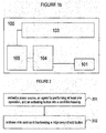
Figure 1b schematically represents components of an apparatus produced according to the present invention. -
Figure 2 presents a flow chart of an embodiment of the process according to the present invention. - In a general embodiment, the slim
electronic apparatus 100 produced according to the present invention comprises apower source 105, anagent 104 for performing at least one operation, anactivation button 101 for initiating said at least one operation by said agent, and anembossed ridge 106 around said button. - Said ridge has at least one interruption, located where a wire or a component of the apparatus is present.
- In a preferred embodiment, said apparatus is embedded in a credit card sized plastic.
- In one embodiment of the apparatus produced according to the present invention, said ridge has the shape of an interrupted circle. In another embodiment of the apparatus produced according to the present invention, said ridge is U-shaped. In yet another embodiment of the apparatus produced according to the present invention, said ridge consists of at least two unconnected segments.
- In a further embodiment of the apparatus produced according to the present invention, said ridge is embossed using at least one standard alphanumerical character or punctuation mark. In one particular embodiment of the apparatus produced according to the present invention, said at least one standard alphanumerical character or punctuation mark comprises an opening parenthesis and a closing parenthesis positioned on opposite sides of said button. In another particular embodiment of the apparatus produced according to the present invention, said at least one standard alphanumerical character or punctuation mark comprises the letter U positioned to contain said button.
- In another embodiment, the apparatus produced according to the present invention further comprises an
output interface 103. In a particular embodiment, said at least one operation comprises generating an authentication credential, and saiduser output interface 103 is adapted to output said authentication credential. In a particular embodiment of the apparatus produced according to the present invention, saidoutput interface 103 is a display, such as an LCD display. In an alternative particular embodiment of the apparatus produced according to the present invention, saidoutput interface 103 generates an audible representation of the credential. - A general embodiment of the process of the present invention for producing a slim electronic apparatus comprises embedding 201 a
power source 105, anagent 104 for performing at least one operation, and an activatingbutton 101 for initiating said at least one operation by said agent, into a card-like housing, and embossing 202 onto said card-like housing aridge 106 around said button. - In a preferred embodiment, said ridge has at least one interruption, located where a wire or a component of the apparatus is present.
- In one embodiment of the process of the present invention, said
ridge 106 is embossed using at least one standard alphanumerical character or punctuation mark. In one particular embodiment of the process of the present invention, said at least one standard alphanumerical character or punctuation mark comprises an opening parenthesis and a closing parenthesis positioned on opposite sides of said button. In another particular embodiment of the process of the present invention, said at least one standard alphanumerical character or punctuation mark comprises the letter U positioned to contain said button. - In a another embodiment of the process of the present invention, said
ridge 106 has the shape of an interrupted circle. In yet another embodiment of the process of the present invention, said ridge is U-shaped. In a further embodiment of the process of the present invention, said ridge consists of at least two unconnected segments. - In another embodiment, the process of the present invention further comprises embedding an
output interface 103 into the card-like housing. In a preferred embodiment, said at least one operation comprises generating an authentication credential, and saidoutput interface 103 is adapted to output said authentication credential. In a particular embodiment of the process of the present invention, saidoutput interface 103 is a display, such as an LCD display. In an alternative particular embodiment of the process of the present invention, saidoutput interface 103 is adapted to generate an audible representation of the credential. - While various embodiments of the present invention have been described above, it should be understood that they have been presented by way of example only, and not limitation.
Claims (10)
- A process for producing a slim electronic apparatus (100), comprising
embedding (201) a power source (105), an agent (104) for performing at least one operation, and an activation button (101) for initiating said at least one operation by said agent (104), into a card-like housing;
characterized in that
the process further comprises embossing (202) onto said card-like housing a ridge (106) around said button (101), wherein said ridge (106) has at least one interruption, said interuption being located where a wire or a component of said apparatus (100) is present. - The process of claim 1, wherein said ridge (106) has the shape of an interrupted circle.
- The process of claim 1, wherein said ridge (106) is U-shaped.
- The process of claim 1, wherein said ridge (106) consists of at least two unconnected segments.
- The process of any of the preceding claims, wherein said ridge (106) is embossed (202) using at least one standard alphanumerical character or punctuation mark.
- The process of claim 5, wherein said at least one standard alphanumerical character or punctuation mark comprises an opening parenthesis and a closing parenthesis positioned on opposite sides of said button (101).
- The process of claim 5, wherein said at least one standard alphanumerical character or punctuation mark comprises the letter U positioned to contain said button (101).
- The process of any of the previous claims, wherein said card-like housing comprises a credit card sized plastic.
- The process of any of the preceding claims, wherein said embedding (201) additionally comprises embedding an output interface (103).
- The process of claim 9, wherein said at least one operation comprises generating an authentication credential, and wherein said output interface (103) is adapted to output said authentication credential.
Applications Claiming Priority (2)
| Application Number | Priority Date | Filing Date | Title |
|---|---|---|---|
| US12/339,636 US8191789B2 (en) | 2008-12-09 | 2008-12-19 | Flex token with embossed key protection |
| PCT/US2009/068646 WO2010080573A1 (en) | 2008-12-19 | 2009-12-18 | Slim electronic apparatus with embossed key protection and process for providing same |
Publications (3)
| Publication Number | Publication Date |
|---|---|
| EP2374096A1 EP2374096A1 (en) | 2011-10-12 |
| EP2374096A4 EP2374096A4 (en) | 2012-06-13 |
| EP2374096B1 true EP2374096B1 (en) | 2014-02-19 |
Family
ID=42316737
Family Applications (1)
| Application Number | Title | Priority Date | Filing Date |
|---|---|---|---|
| EP09837961.3A Not-in-force EP2374096B1 (en) | 2008-12-19 | 2009-12-18 | Process for providing a slim electronic apparatus with embossed key protection |
Country Status (4)
| Country | Link |
|---|---|
| US (1) | US8191789B2 (en) |
| EP (1) | EP2374096B1 (en) |
| CN (1) | CN102257517B (en) |
| WO (1) | WO2010080573A1 (en) |
Families Citing this family (3)
| Publication number | Priority date | Publication date | Assignee | Title |
|---|---|---|---|---|
| US10176419B1 (en) * | 2009-04-06 | 2019-01-08 | Dynamics Inc. | Cards and assemblies with user interfaces |
| US9235299B2 (en) | 2013-02-06 | 2016-01-12 | Google Technology Holdings LLC | Touch sensitive surface for an electronic device with false touch protection |
| US10937263B1 (en) * | 2018-09-27 | 2021-03-02 | Amazon Technologies, Inc. | Smart credentials for protecting personal information |
Family Cites Families (18)
| Publication number | Priority date | Publication date | Assignee | Title |
|---|---|---|---|---|
| US4100011A (en) | 1975-08-04 | 1978-07-11 | Addressograph Multigraph Corp. | Production of laminated card with printed magnetically encodable stripe |
| DE8509315U1 (en) * | 1985-03-28 | 1985-05-15 | Triumph-Adler Aktiengesellschaft für Büro- und Informationstechnik, 8500 Nürnberg | Safety device for buttons |
| US4686898A (en) | 1986-01-21 | 1987-08-18 | National Business Systems, Inc. | Credit card embossing system |
| US5368941A (en) * | 1992-08-31 | 1994-11-29 | Dow Corning Corporation | Deformable, abrasion-resistant silicone coating and method of producing the same |
| US5636271A (en) * | 1995-06-14 | 1997-06-03 | Mci Corporation | Security code selector for telephone access card |
| JP2001167242A (en) | 1999-12-10 | 2001-06-22 | Sony Corp | Embossable IC card, method of manufacturing the same, and information reading and checking system thereof |
| US6471127B2 (en) * | 2000-07-06 | 2002-10-29 | Bank Of America Corporation | Data card |
| USD467245S1 (en) * | 2000-07-17 | 2002-12-17 | Lintel Security S.A. | Device for securing banking operations |
| US6776332B2 (en) * | 2002-12-26 | 2004-08-17 | Micropin Technologies Inc. | System and method for validating and operating an access card |
| DE20313096U1 (en) * | 2003-08-25 | 2005-01-05 | Dewert Antriebs- Und Systemtechnik Gmbh & Co. Kg | Remote control for electric motor driven furniture, using handheld remote control unit connected to electric motor and coupling via respective transmission media |
| DE102005008258A1 (en) * | 2004-04-07 | 2005-10-27 | Giesecke & Devrient Gmbh | Data carrier with TAN generator and display |
| KR100540780B1 (en) * | 2004-12-15 | 2006-01-11 | 주식회사 삼영테크놀로지 | Integral acrylic keypad with integral acrylic touchpad |
| WO2006107862A2 (en) | 2005-04-04 | 2006-10-12 | Mastercard International Incorporated | A system and method enabling fourth line embossing on contactless cards |
| US8266441B2 (en) * | 2005-04-22 | 2012-09-11 | Bank Of America Corporation | One-time password credit/debit card |
| FR2893163B1 (en) | 2005-11-08 | 2008-02-01 | Oberthur Card Syst Sa | METHOD FOR MANUFACTURING A MICROCIRCUIT CARD AND A MICROCIRCUIT CARD, IN PARTICULAR A MAGNETIC ANTENNA. |
| IL175824A0 (en) | 2006-05-22 | 2007-09-20 | On Track Innovations Ltd | Data transaction card having a tunable coil antenna with reduced footprint |
| FR2913809B1 (en) | 2007-03-14 | 2009-06-05 | Nicomatic Sa Sa | PUSH BUTTON TYPE SWITCH, AND PRINTED CIRCUIT INCLUDING THE SAME |
| US8125341B2 (en) * | 2007-12-10 | 2012-02-28 | Checkpoint Systems, Inc. | Resonant tag with reinforced deactivation dimple |
-
2008
- 2008-12-19 US US12/339,636 patent/US8191789B2/en not_active Expired - Fee Related
-
2009
- 2009-12-18 EP EP09837961.3A patent/EP2374096B1/en not_active Not-in-force
- 2009-12-18 CN CN200980151160.3A patent/CN102257517B/en not_active Expired - Fee Related
- 2009-12-18 WO PCT/US2009/068646 patent/WO2010080573A1/en not_active Ceased
Also Published As
| Publication number | Publication date |
|---|---|
| US20100140360A1 (en) | 2010-06-10 |
| CN102257517B (en) | 2014-01-29 |
| EP2374096A4 (en) | 2012-06-13 |
| EP2374096A1 (en) | 2011-10-12 |
| US8191789B2 (en) | 2012-06-05 |
| CN102257517A (en) | 2011-11-23 |
| WO2010080573A1 (en) | 2010-07-15 |
Similar Documents
| Publication | Publication Date | Title |
|---|---|---|
| US6257486B1 (en) | Smart card pin system, card, and reader | |
| US7493288B2 (en) | RF payment via a mobile device | |
| US7228155B2 (en) | System and method for remotely initializing a RF transaction | |
| KR101259925B1 (en) | One-time password credit/debit card | |
| US20040085188A1 (en) | Individual authentication device and cellular terminal apparatus | |
| US20090199004A1 (en) | System and method for self-authenticating token | |
| US20100140358A1 (en) | Slim electronic device with detector for unintentional activation | |
| CN114341876A (en) | Registration device for biometric smart card | |
| TWI582703B (en) | Auxiliary mounting structure for mounting advanced smart card | |
| JP2010504583A (en) | Electronic card and manufacturing method thereof | |
| EP2248093A2 (en) | Financial transaction token | |
| WO2022211702A1 (en) | A biometric system comprising a contactless smartcard and an enrollment assistance device, and a method for enrolling a user having the system | |
| CN101452539A (en) | Mobile identification method based on NFC | |
| CN101504731B (en) | Movable recognition system based on NFC | |
| US8191789B2 (en) | Flex token with embossed key protection | |
| US20100102131A1 (en) | Systems and Methods for Disabling a Contactless Transaction Device | |
| CN103793741B (en) | Display card with protective chip | |
| TW201638829A (en) | Auxiliary mounting structure for mounting advanced smart card | |
| CN109094221A (en) | A kind of one body seal of physical electronic | |
| US11526718B2 (en) | Method of manufacturing mini smart card | |
| CN208433018U (en) | Secure payment card | |
| JP2000326668A (en) | Method for producing molded card and molded card base material | |
| CN203166952U (en) | Bank IC card type dynamic password security code token device | |
| CN112633452A (en) | Light and thin intelligent card and manufacturing method thereof | |
| KR200335758Y1 (en) | Luminous Plastic Card |
Legal Events
| Date | Code | Title | Description |
|---|---|---|---|
| PUAI | Public reference made under article 153(3) epc to a published international application that has entered the european phase |
Free format text: ORIGINAL CODE: 0009012 |
|
| 17P | Request for examination filed |
Effective date: 20110708 |
|
| AK | Designated contracting states |
Kind code of ref document: A1 Designated state(s): AT BE BG CH CY CZ DE DK EE ES FI FR GB GR HR HU IE IS IT LI LT LU LV MC MK MT NL NO PL PT RO SE SI SK SM TR |
|
| DAX | Request for extension of the european patent (deleted) | ||
| A4 | Supplementary search report drawn up and despatched |
Effective date: 20120510 |
|
| RIC1 | Information provided on ipc code assigned before grant |
Ipc: G06K 19/077 20060101AFI20120504BHEP Ipc: H01H 9/00 20060101ALI20120504BHEP Ipc: G06F 3/00 20060101ALI20120504BHEP |
|
| GRAP | Despatch of communication of intention to grant a patent |
Free format text: ORIGINAL CODE: EPIDOSNIGR1 |
|
| INTG | Intention to grant announced |
Effective date: 20130906 |
|
| GRAS | Grant fee paid |
Free format text: ORIGINAL CODE: EPIDOSNIGR3 |
|
| GRAA | (expected) grant |
Free format text: ORIGINAL CODE: 0009210 |
|
| AK | Designated contracting states |
Kind code of ref document: B1 Designated state(s): AT BE BG CH CY CZ DE DK EE ES FI FR GB GR HR HU IE IS IT LI LT LU LV MC MK MT NL NO PL PT RO SE SI SK SM TR |
|
| REG | Reference to a national code |
Ref country code: GB Ref legal event code: FG4D |
|
| REG | Reference to a national code |
Ref country code: CH Ref legal event code: EP |
|
| REG | Reference to a national code |
Ref country code: AT Ref legal event code: REF Ref document number: 652916 Country of ref document: AT Kind code of ref document: T Effective date: 20140315 |
|
| REG | Reference to a national code |
Ref country code: DE Ref legal event code: R096 Ref document number: 602009021937 Country of ref document: DE Effective date: 20140403 |
|
| REG | Reference to a national code |
Ref country code: IE Ref legal event code: FG4D |
|
| REG | Reference to a national code |
Ref country code: NL Ref legal event code: VDEP Effective date: 20140219 |
|
| REG | Reference to a national code |
Ref country code: AT Ref legal event code: MK05 Ref document number: 652916 Country of ref document: AT Kind code of ref document: T Effective date: 20140219 |
|
| REG | Reference to a national code |
Ref country code: LT Ref legal event code: MG4D |
|
| PG25 | Lapsed in a contracting state [announced via postgrant information from national office to epo] |
Ref country code: NO Free format text: LAPSE BECAUSE OF FAILURE TO SUBMIT A TRANSLATION OF THE DESCRIPTION OR TO PAY THE FEE WITHIN THE PRESCRIBED TIME-LIMIT Effective date: 20140519 Ref country code: LT Free format text: LAPSE BECAUSE OF FAILURE TO SUBMIT A TRANSLATION OF THE DESCRIPTION OR TO PAY THE FEE WITHIN THE PRESCRIBED TIME-LIMIT Effective date: 20140219 Ref country code: IS Free format text: LAPSE BECAUSE OF FAILURE TO SUBMIT A TRANSLATION OF THE DESCRIPTION OR TO PAY THE FEE WITHIN THE PRESCRIBED TIME-LIMIT Effective date: 20140619 |
|
| PG25 | Lapsed in a contracting state [announced via postgrant information from national office to epo] |
Ref country code: ES Free format text: LAPSE BECAUSE OF FAILURE TO SUBMIT A TRANSLATION OF THE DESCRIPTION OR TO PAY THE FEE WITHIN THE PRESCRIBED TIME-LIMIT Effective date: 20140219 Ref country code: NL Free format text: LAPSE BECAUSE OF FAILURE TO SUBMIT A TRANSLATION OF THE DESCRIPTION OR TO PAY THE FEE WITHIN THE PRESCRIBED TIME-LIMIT Effective date: 20140219 Ref country code: CY Free format text: LAPSE BECAUSE OF FAILURE TO SUBMIT A TRANSLATION OF THE DESCRIPTION OR TO PAY THE FEE WITHIN THE PRESCRIBED TIME-LIMIT Effective date: 20140219 Ref country code: PT Free format text: LAPSE BECAUSE OF FAILURE TO SUBMIT A TRANSLATION OF THE DESCRIPTION OR TO PAY THE FEE WITHIN THE PRESCRIBED TIME-LIMIT Effective date: 20140619 Ref country code: SE Free format text: LAPSE BECAUSE OF FAILURE TO SUBMIT A TRANSLATION OF THE DESCRIPTION OR TO PAY THE FEE WITHIN THE PRESCRIBED TIME-LIMIT Effective date: 20140219 Ref country code: AT Free format text: LAPSE BECAUSE OF FAILURE TO SUBMIT A TRANSLATION OF THE DESCRIPTION OR TO PAY THE FEE WITHIN THE PRESCRIBED TIME-LIMIT Effective date: 20140219 Ref country code: FI Free format text: LAPSE BECAUSE OF FAILURE TO SUBMIT A TRANSLATION OF THE DESCRIPTION OR TO PAY THE FEE WITHIN THE PRESCRIBED TIME-LIMIT Effective date: 20140219 |
|
| PG25 | Lapsed in a contracting state [announced via postgrant information from national office to epo] |
Ref country code: BE Free format text: LAPSE BECAUSE OF FAILURE TO SUBMIT A TRANSLATION OF THE DESCRIPTION OR TO PAY THE FEE WITHIN THE PRESCRIBED TIME-LIMIT Effective date: 20140219 Ref country code: LV Free format text: LAPSE BECAUSE OF FAILURE TO SUBMIT A TRANSLATION OF THE DESCRIPTION OR TO PAY THE FEE WITHIN THE PRESCRIBED TIME-LIMIT Effective date: 20140219 Ref country code: HR Free format text: LAPSE BECAUSE OF FAILURE TO SUBMIT A TRANSLATION OF THE DESCRIPTION OR TO PAY THE FEE WITHIN THE PRESCRIBED TIME-LIMIT Effective date: 20140219 |
|
| PG25 | Lapsed in a contracting state [announced via postgrant information from national office to epo] |
Ref country code: RO Free format text: LAPSE BECAUSE OF FAILURE TO SUBMIT A TRANSLATION OF THE DESCRIPTION OR TO PAY THE FEE WITHIN THE PRESCRIBED TIME-LIMIT Effective date: 20140219 Ref country code: CZ Free format text: LAPSE BECAUSE OF FAILURE TO SUBMIT A TRANSLATION OF THE DESCRIPTION OR TO PAY THE FEE WITHIN THE PRESCRIBED TIME-LIMIT Effective date: 20140219 Ref country code: EE Free format text: LAPSE BECAUSE OF FAILURE TO SUBMIT A TRANSLATION OF THE DESCRIPTION OR TO PAY THE FEE WITHIN THE PRESCRIBED TIME-LIMIT Effective date: 20140219 Ref country code: DK Free format text: LAPSE BECAUSE OF FAILURE TO SUBMIT A TRANSLATION OF THE DESCRIPTION OR TO PAY THE FEE WITHIN THE PRESCRIBED TIME-LIMIT Effective date: 20140219 |
|
| REG | Reference to a national code |
Ref country code: DE Ref legal event code: R097 Ref document number: 602009021937 Country of ref document: DE |
|
| PG25 | Lapsed in a contracting state [announced via postgrant information from national office to epo] |
Ref country code: SK Free format text: LAPSE BECAUSE OF FAILURE TO SUBMIT A TRANSLATION OF THE DESCRIPTION OR TO PAY THE FEE WITHIN THE PRESCRIBED TIME-LIMIT Effective date: 20140219 Ref country code: PL Free format text: LAPSE BECAUSE OF FAILURE TO SUBMIT A TRANSLATION OF THE DESCRIPTION OR TO PAY THE FEE WITHIN THE PRESCRIBED TIME-LIMIT Effective date: 20140219 |
|
| PLBE | No opposition filed within time limit |
Free format text: ORIGINAL CODE: 0009261 |
|
| STAA | Information on the status of an ep patent application or granted ep patent |
Free format text: STATUS: NO OPPOSITION FILED WITHIN TIME LIMIT |
|
| 26N | No opposition filed |
Effective date: 20141120 |
|
| REG | Reference to a national code |
Ref country code: DE Ref legal event code: R097 Ref document number: 602009021937 Country of ref document: DE Effective date: 20141120 |
|
| PG25 | Lapsed in a contracting state [announced via postgrant information from national office to epo] |
Ref country code: IT Free format text: LAPSE BECAUSE OF FAILURE TO SUBMIT A TRANSLATION OF THE DESCRIPTION OR TO PAY THE FEE WITHIN THE PRESCRIBED TIME-LIMIT Effective date: 20140219 |
|
| PG25 | Lapsed in a contracting state [announced via postgrant information from national office to epo] |
Ref country code: SI Free format text: LAPSE BECAUSE OF FAILURE TO SUBMIT A TRANSLATION OF THE DESCRIPTION OR TO PAY THE FEE WITHIN THE PRESCRIBED TIME-LIMIT Effective date: 20140219 |
|
| PG25 | Lapsed in a contracting state [announced via postgrant information from national office to epo] |
Ref country code: LU Free format text: LAPSE BECAUSE OF FAILURE TO SUBMIT A TRANSLATION OF THE DESCRIPTION OR TO PAY THE FEE WITHIN THE PRESCRIBED TIME-LIMIT Effective date: 20141218 |
|
| REG | Reference to a national code |
Ref country code: IE Ref legal event code: MM4A |
|
| PG25 | Lapsed in a contracting state [announced via postgrant information from national office to epo] |
Ref country code: IE Free format text: LAPSE BECAUSE OF NON-PAYMENT OF DUE FEES Effective date: 20141218 |
|
| REG | Reference to a national code |
Ref country code: FR Ref legal event code: PLFP Year of fee payment: 7 |
|
| PG25 | Lapsed in a contracting state [announced via postgrant information from national office to epo] |
Ref country code: SM Free format text: LAPSE BECAUSE OF FAILURE TO SUBMIT A TRANSLATION OF THE DESCRIPTION OR TO PAY THE FEE WITHIN THE PRESCRIBED TIME-LIMIT Effective date: 20140219 |
|
| PG25 | Lapsed in a contracting state [announced via postgrant information from national office to epo] |
Ref country code: MC Free format text: LAPSE BECAUSE OF FAILURE TO SUBMIT A TRANSLATION OF THE DESCRIPTION OR TO PAY THE FEE WITHIN THE PRESCRIBED TIME-LIMIT Effective date: 20140219 |
|
| PG25 | Lapsed in a contracting state [announced via postgrant information from national office to epo] |
Ref country code: GR Free format text: LAPSE BECAUSE OF FAILURE TO SUBMIT A TRANSLATION OF THE DESCRIPTION OR TO PAY THE FEE WITHIN THE PRESCRIBED TIME-LIMIT Effective date: 20140520 Ref country code: BG Free format text: LAPSE BECAUSE OF FAILURE TO SUBMIT A TRANSLATION OF THE DESCRIPTION OR TO PAY THE FEE WITHIN THE PRESCRIBED TIME-LIMIT Effective date: 20140219 |
|
| PG25 | Lapsed in a contracting state [announced via postgrant information from national office to epo] |
Ref country code: MT Free format text: LAPSE BECAUSE OF FAILURE TO SUBMIT A TRANSLATION OF THE DESCRIPTION OR TO PAY THE FEE WITHIN THE PRESCRIBED TIME-LIMIT Effective date: 20140219 Ref country code: HU Free format text: LAPSE BECAUSE OF FAILURE TO SUBMIT A TRANSLATION OF THE DESCRIPTION OR TO PAY THE FEE WITHIN THE PRESCRIBED TIME-LIMIT; INVALID AB INITIO Effective date: 20091218 Ref country code: TR Free format text: LAPSE BECAUSE OF FAILURE TO SUBMIT A TRANSLATION OF THE DESCRIPTION OR TO PAY THE FEE WITHIN THE PRESCRIBED TIME-LIMIT Effective date: 20140219 |
|
| REG | Reference to a national code |
Ref country code: FR Ref legal event code: PLFP Year of fee payment: 8 |
|
| REG | Reference to a national code |
Ref country code: FR Ref legal event code: PLFP Year of fee payment: 9 |
|
| PG25 | Lapsed in a contracting state [announced via postgrant information from national office to epo] |
Ref country code: MK Free format text: LAPSE BECAUSE OF FAILURE TO SUBMIT A TRANSLATION OF THE DESCRIPTION OR TO PAY THE FEE WITHIN THE PRESCRIBED TIME-LIMIT Effective date: 20140219 |
|
| PGFP | Annual fee paid to national office [announced via postgrant information from national office to epo] |
Ref country code: FR Payment date: 20201112 Year of fee payment: 12 Ref country code: GB Payment date: 20201209 Year of fee payment: 12 Ref country code: DE Payment date: 20201208 Year of fee payment: 12 Ref country code: CH Payment date: 20201215 Year of fee payment: 12 |
|
| REG | Reference to a national code |
Ref country code: DE Ref legal event code: R119 Ref document number: 602009021937 Country of ref document: DE |
|
| REG | Reference to a national code |
Ref country code: CH Ref legal event code: PL |
|
| GBPC | Gb: european patent ceased through non-payment of renewal fee |
Effective date: 20211218 |
|
| PG25 | Lapsed in a contracting state [announced via postgrant information from national office to epo] |
Ref country code: GB Free format text: LAPSE BECAUSE OF NON-PAYMENT OF DUE FEES Effective date: 20211218 Ref country code: DE Free format text: LAPSE BECAUSE OF NON-PAYMENT OF DUE FEES Effective date: 20220701 |
|
| PG25 | Lapsed in a contracting state [announced via postgrant information from national office to epo] |
Ref country code: FR Free format text: LAPSE BECAUSE OF NON-PAYMENT OF DUE FEES Effective date: 20211231 |
|
| PG25 | Lapsed in a contracting state [announced via postgrant information from national office to epo] |
Ref country code: LI Free format text: LAPSE BECAUSE OF NON-PAYMENT OF DUE FEES Effective date: 20211231 Ref country code: CH Free format text: LAPSE BECAUSE OF NON-PAYMENT OF DUE FEES Effective date: 20211231 |