EP2372835A1 - Multibeam antenna device - Google Patents
Multibeam antenna device Download PDFInfo
- Publication number
- EP2372835A1 EP2372835A1 EP09829186A EP09829186A EP2372835A1 EP 2372835 A1 EP2372835 A1 EP 2372835A1 EP 09829186 A EP09829186 A EP 09829186A EP 09829186 A EP09829186 A EP 09829186A EP 2372835 A1 EP2372835 A1 EP 2372835A1
- Authority
- EP
- European Patent Office
- Prior art keywords
- rotman lens
- output ports
- antenna
- input ports
- array antenna
- Prior art date
- Legal status (The legal status is an assumption and is not a legal conclusion. Google has not performed a legal analysis and makes no representation as to the accuracy of the status listed.)
- Ceased
Links
Images


Classifications
-
- H—ELECTRICITY
- H01—ELECTRIC ELEMENTS
- H01Q—ANTENNAS, i.e. RADIO AERIALS
- H01Q21/00—Antenna arrays or systems
- H01Q21/29—Combinations of different interacting antenna units for giving a desired directional characteristic
-
- H—ELECTRICITY
- H01—ELECTRIC ELEMENTS
- H01Q—ANTENNAS, i.e. RADIO AERIALS
- H01Q13/00—Waveguide horns or mouths; Slot antennas; Leaky-waveguide antennas; Equivalent structures causing radiation along the transmission path of a guided wave
- H01Q13/20—Non-resonant leaky-waveguide or transmission-line antennas; Equivalent structures causing radiation along the transmission path of a guided wave
- H01Q13/206—Microstrip transmission line antennas
-
- H—ELECTRICITY
- H01—ELECTRIC ELEMENTS
- H01Q—ANTENNAS, i.e. RADIO AERIALS
- H01Q19/00—Combinations of primary active antenna elements and units with secondary devices, e.g. with quasi-optical devices, for giving the antenna a desired directional characteristic
- H01Q19/06—Combinations of primary active antenna elements and units with secondary devices, e.g. with quasi-optical devices, for giving the antenna a desired directional characteristic using refracting or diffracting devices, e.g. lens
-
- H—ELECTRICITY
- H01—ELECTRIC ELEMENTS
- H01Q—ANTENNAS, i.e. RADIO AERIALS
- H01Q21/00—Antenna arrays or systems
- H01Q21/06—Arrays of individually energised antenna units similarly polarised and spaced apart
- H01Q21/061—Two dimensional planar arrays
- H01Q21/064—Two dimensional planar arrays using horn or slot aerials
-
- H—ELECTRICITY
- H01—ELECTRIC ELEMENTS
- H01Q—ANTENNAS, i.e. RADIO AERIALS
- H01Q21/00—Antenna arrays or systems
- H01Q21/06—Arrays of individually energised antenna units similarly polarised and spaced apart
- H01Q21/061—Two dimensional planar arrays
- H01Q21/065—Patch antenna array
-
- H—ELECTRICITY
- H01—ELECTRIC ELEMENTS
- H01Q—ANTENNAS, i.e. RADIO AERIALS
- H01Q25/00—Antennas or antenna systems providing at least two radiating patterns
- H01Q25/007—Antennas or antenna systems providing at least two radiating patterns using two or more primary active elements in the focal region of a focusing device
- H01Q25/008—Antennas or antenna systems providing at least two radiating patterns using two or more primary active elements in the focal region of a focusing device lens fed multibeam arrays
Definitions
- the present invention relates to a design method for a Rotman lens usable in a multi-beam antenna device utilizable for millimeter band signal transmitting/receiving.
- the reference numeral (1) denotes a Rotman lens.
- the reference numerals (21),(22), --- (2m) denote respective ones of a plurality of input ports for feeding electric power, and the reference numerals (31),(32), --- (3n) denote respective ones of a plurality of output ports for extracting electric power in the Rotman lens (1).
- the reference numerals (41),(42), --- (4n) denote respective ones of a plurality of antenna elements for radiating electromagnetic waves to space
- the reference numeral (5) denotes an array antenna having the plurality of antenna elements (41),(42), --- (4n) arranged linearly.
- the reference numerals (61),(62), --- (6n) denote respective ones of a plurality of transmission lines connecting respective ones of the output ports to respective ones of the antenna elements
- the reference numeral (7) denotes a line section comprised of the transmission lines (61),(62), --- (6n) having different lengths.
- the reference numeral (8) denotes a center line. This antenna device is line-symmetric with respect to the center line (8).
- the reference numeral (9) denotes an auxiliary line for indicating a position of one (21) of the input ports.
- the input port (21) is located in a direction at an elevation angle ⁇ with respect to the center line (8) when viewed from S2 which is an origin of an X-Y coordinate system.
- the reference numeral (10) denotes a straight line which is indicative of a spatial beam direction upon excitation of the input port (21), and oriented in a direction at an angle ⁇ with respect to a direction facing a front of the array antenna.
- the input ports (21),(22), --- (2m) are arranged on an arc having a radius R from a center located at a focal point S1 of the Rotman lens.
- the origin S2 of the X-Y coordinate system is represented by an intersecting point of the center line (8) with a curve segment having the output ports (31), (32), ---, (3n) arranged thereon.
- S3 indicates an intersecting point of the center line (8) with a curve segment having the input ports (21), (22), ---, (2m) arranged thereon.
- An x coordinate and a y coordinate of each of the output ports (31),(32),-(3n), and an electrical length w of each of the transmission lines (61),(62), --- (6n) are expressed in the following Formulas 1 to 3, respectively:
- R F ⁇ a 0 - G 2 + F 2 ⁇ b 0 2 / 2 ⁇ G - F ⁇ a 0
- G is a size of the Rotman lens defined by a distance between S2 and S3.
- F is a distance between the input port (21) and S2, and 2 Ln is an aperture length of the array antenna (5).
- the radicand inside the radical symbol in the Formula 3 is required to have a positive sign or to be zero. In other words, the following Formula 5 has to be satisfied.
- the multi-beam antenna device is further characterized in that the Rotman lens is formed using a triplate.
- the multi-beam antenna device is further characterized in that the array antenna is formed using a triplate.
- the multi-beam antenna device is further characterized in that each of the input ports is partially formed as two branched transmission lines to distribute and feed electric power.
- a multi-beam antenna device of the present invention comprises: a Rotman lens having a plurality of input ports (21), (22), ---, (2m) for feeding electric power, and a plurality of output ports (31), (32), ---, (3n) for extracting the electric power from the input ports; an array antenna comprised of a plurality of antenna elements and adapted to radiate electromagnetic waves to space; and a plurality of transmission lines connecting respective ones of the output ports to respective ones of the antenna elements, wherein a curve for arranging the output ports thereon and a length of each of the transmission lines are set such that, when a given one of the input ports is excited, a beam is formed in a direction at an angle corresponding to that of the given input port.
- a multi-beam antenna device of the present invention comprises: a Rotman lens having a plurality of input ports (21), (22), ---, (2m) for feeding electric power, and a plurality of output ports (31), (32), ---, (3n) for extracting the electric power from the input ports; an array antenna comprised of a plurality of antenna elements and adapted to radiate electromagnetic waves to space; and a plurality of transmission lines connecting respective ones of the output ports to respective ones of the antenna elements, wherein a curve for arranging the output ports thereon and a length of each of the transmission lines are set such that, when a given one of the input ports is excited, a beam is formed in a direction at an angle corresponding to that of the given input port.
- a 1 - ⁇ 2 - g - 1 / g - a 0 2
- b 2 ⁇ g ⁇ g - 1 / g - a 0 - g - 1 / g - a 0 2 ⁇ b 0 2 ⁇ ⁇ 2 + 2 ⁇ ⁇ 2 - 2 ⁇ g
- c g ⁇ b 0 2 ⁇ ⁇ 2 / g - a 0 - b 0 4 ⁇ ⁇ 4 / 4 ⁇ g - a 0 2 - ⁇ 2
- g G / F
- ⁇ ⁇ / ⁇ ⁇ ° Ln / F
- a 0 cos ⁇
- + b 0 sin ⁇ .
- an in-vehicle multi-beam antenna device of the present invention comprises: a Rotman lens having a plurality of input ports (21), (22), ---, (2m) for feeding electric power, and a plurality of output ports (31), (32), ---, (3n) for extracting the electric power from the input ports; an array antenna comprised of a plurality of antenna elements and each adapted to radiate electromagnetic waves to space; and a plurality of transmission lines connecting respective ones of the output ports to respective ones of the antenna elements, wherein a curve for arranging the output ports thereon and a length of each of the transmission lines are set such that, when a given one of the input ports is excited, a beam is formed in a direction at an angle corresponding to that of the given input port.
- the multi-beam antenna device is characterized in that ⁇ with respect to ⁇ is set to satisfy the following relation: ⁇ ⁇ ⁇ , where: ⁇ is a spatial beam-forming angle of the array antenna when viewed from a direction facing a front of the array antenna; and ⁇ is an angle between a center line (8) of the Rotman lens, and a line segment which connects one of the input ports and an intersecting point S2 of the center line (8) with a curve segment having the output ports (31), (32), ---, (3n) arranged thereon.
- ⁇ Ln /2
- the multi-beam antenna of the present invention which is designed based on respective coordinates (x, y) of the output ports (31), (32), ---, (3n) and respective electrical lengths w of the transmission lines (61),(62), --- (6n), each calculated using the Formulas 1 to 4, when electric power is fed from a given one of the input ports which has an angle ⁇ when viewed from S2, a phase inclination of a line representing respective excitation phases at the antenna elements (41),(42), --- (4n) on the basis of that at an aperture center of the array antenna (5), as indicated by the straight line 2 in FIG. 7 , is reduced by one-half as compared with the straight line 1 in FIG.
- the Rotman lens may be formed in a triplate structure.
- a taper shape in complicated input and output port sections, and a phase-adjusting transmission line section (7) can be easily formed by means of etching or the like, and a first connection section (58) of the array antenna (5) and a connection port sub-section (16) of the transmission line section (7) can be electromagnetically coupled together via a first connection hole (59) provided in a first ground conductor (53).
- the antenna array may also be formed in a triplate structure.
- the array antenna in the multi-beam antenna device according to the first embodiment is formed as a triplate-structured array antenna by laminating a slotted plate (50) and a feeder line (57) of an antenna substrate (52), and the first ground conductor (53) together through a dielectric (71a, 71b) interposed between adjacent ones thereof. Based on employing this structure, it becomes possible to make up a low-loss multi-beam antenna device with a simple laminated structure of all components thereof.
- a radiation element (56) formed in the antenna substrate (52) illustrated in FIG. 3 can radiate an electromagnetic wave having a desired frequency in cooperation with the first ground conductor (53) and a slot (54) formed in the slot plate (50), illustrated in FIG. 2 , to serve as the antenna element.
- a plurality of the antenna elements are arranged to form the array antenna (5) as a whole.
- a triplate-structured Rotman lens is made up of the first ground conductor (53), the Rotman lens substrate (12) and a second ground conductor (13), illustrated in FIG. 2 . More specifically, as illustrated in FIG.
- the triplate-structured Rotman lens is formed by laminating the first ground conductor (53), the transmission line section (7) of the Rotman lens substrate (12), and the second ground conductor (13) together through a dielectric (71a, 71b) interposed between adjacent ones thereof.
- the first connection section (58) formed in the antenna substrate (52) is electromagnetically coupled with the connection port sub-section (16) of the transmission line section (7) formed in the Rotman lens substrate (12) illustrated in FIG. 4 , through the first connection hole (59) formed in the first ground conductor (53), so that desired exciting electric power is transmitted from the output ports of the Rotman lens (1) to the array antenna (5).
- each of a metal spacer (51a, 51b) disposed on a respective one of upper and lower sides of the antenna substrate (52) and a metal spacer (11a, 11b) disposed a respective one of upper and lower sides of the Rotman lens substrate (12) holds a respective one of the antenna substrate (52) and the Rotman lens substrate (12) in a spaced manner, while forming a metal wall around an electromagnetic coupling region between the first connection section (58) formed in the antenna substrate (52) and the connection port sub-section (16) of the transmission line section (7) formed in the Rotman lens substrate (12), so that they can contribute to efficient transmission of electric power without leakage to the surroundings, so as to achieve low-loss characteristics even at high frequencies.
- each of a void (55a, 55b) in the metal spacer (51a, 51b) and a void (14a, 14b) in the metal spacers (11a, 11a) may be filled with a dielectric (71a, 71b).
- the metal spacer (11a, 11b) also forms a metal wall around the input port section (17) of the antenna device, so that it can contribute to efficient transmission of electric power to a high-frequency circuit through a second connection hole (15) formed in the second ground conductor (13) without leakage to the surroundings, so as to achieve low-loss characteristics even at high frequencies.
- Each of the first connection hole (59) and the second connection hole (15) may be formed as a waveguide opening suited to a frequency band to be used.
- transmission/receiving of electric power is performed by means of electromagnetic coupling, so that it is not necessary to ensure high positional accuracy during assembly at a level of conventional assembly accuracy.
- a flexible substrate prepared by laminating a polyimide film to a copper foil is employed, wherein the radiation element (56), the feeder line (57), the first connection section (58), the Rotman lens (1), the transmission line section (7), the connection port sub-section (16) of the transmission line section (7), and the input port section (17) of the antenna device, are formed by etchingly removing an unnecessary part of the copper foil.
- the flexible substrate may be prepared by employing a film as a base material and laminating a metal foil, such as a copper foil, onto the film.
- a metal foil such as a copper foil
- the radiation elements and a plurality of the feeder lines connecting therebetween may be formed by etchingly removing an unnecessary part of the copper foil (metal foil).
- the flexible substrate may be made up using a copper-cladded laminate prepared by laminating a copper foil on a thin resin sheet consisting of a glass cloth impregnated with resin.
- the film may be made of a material, such as polyethylene, polypropylene, polytetrafluoroethylene, ethylene fluoride-polypropylene copolymer, ethylene-tetrafluoroethylene copolymer, polyamide, polyimide, polyamide-imide, polyarylate, thermoplastic polyimide, polyetherimide, polyether ether ketone, polyethylene terephthalate, polybutylene terephthalate, polystyrene, polysulfone, polyphenylene ether, polyphenylene sulfide, or polymethylpentene.
- An adhesive may be used for lamination between the film and the metal foil.
- a flexible substrate prepared by laminating a polyimide film to a copper foil.
- a fluorine-based film is preferably used.
- a metal plate or a coated plastic plate may be used as the ground conductor or the metal spacer for use in the multi-beam antenna device according to the first embodiment. Particularly, it is preferable to use an aluminum plate in view of an advantage of being able to produce the ground conductor or the metal spacer in a low weight and at a low cost.
- the ground conductor or the metal spacer may be made up using a flexible substrate prepared by employing a film as a base material and laminating a copper foil onto the film, or a copper-cladded laminate prepared by laminating a copper foil on a thin resin sheet consisting of a glass cloth impregnated with resin.
- a slot or coupling hole-forming section formed in the ground conductor may be formed by punching based on mechanical press or by etching. In view of simplicity, productivity, etc., the punching based on mechanical press is preferable.
- the substrate-supporting dielectric (71a, 71b) for use in the multi-beam antenna device according to the first embodiment it is preferable to use a foamed material having a small relative permittivity with respect to air.
- the foamed material may include: a polyolefin-based foamed material such as polyethylene or polypropylene; a polystyrene-based foamed material; a polyurethane-based foamed material a polysilicone-based foamed material; and a rubber-based foamed material.
- a polyolefin-based foamed material is preferable, because it is lower in the relative permittivity with respect to air.
- the multi-beam antenna device according to the first embodiment will be further viewed in terms of dimensions of each member, etc., and described as a second embodiment with reference to FIG. 2 .
- Each of the slotted plate (50), the first ground conductor (53), the second ground conductor (13), the metal spacer (51a, 51b), and the metal spacer (11a, 11b), is made up using an aluminum plate having a thickness of 0.3 mm.
- the substrate-supporting dielectric (71a, 71b) is made up using a polyethylene foam having a thickness of 0.3 mm and a relative permittivity of about 1.1.
- Each of the antenna substrate (52) and the Rotman lens substrate (12) is made up using a flexible substrate prepared by laminating a copper foil (having a thickness, for example, of 25 ⁇ m) to a polyimide film (having a thickness, for example, of 25 ⁇ m), wherein the radiation element (56), the feeder line (57), the first connection section (58), the Rotman lens (1), the transmission line section (7), the connection port sub-section (16) of the transmission line section (7), and the input port section (17), are formed by etchingly removing an unnecessary part of the copper foil.
- Each of all of the ground conductors, the slotted plate and all of the metal spacers is made up using an aluminum plate subjected to punching based on mechanical press.
- each of the first connection hole (59) formed in the first ground conductor (53) and the second connection hole (15) formed in the second ground conductor (13) is formed as a waveguide opening having a size of 1.25 mm length ⁇ 2.53 mm width.
- the multi-beam antenna device according to the second embodiment is improved in relative gain by 2.5 dB or more, in comparison on the basis of a loss in a multi-beam antenna device formed by the conventional design process, so that it can achieve excellent characteristics.
- a connection portion of each of a plurality of input ports (521),(522), --- (52m) is formed as a two branched transmission lines to distribute and feed electric power, which allows the electric power fed from the input ports into a Rotman lens (1) to be concentrated in a central region of a plurality of output ports (531),(532), --- (53n), so as to suppress dispersion of the electric power toward a region devoid of the output ports (531),(532), --- (53n) in a curve segment having the output ports arranged thereon.
- One feature of the present invention is that the present invention makes it possible to design a Rotman lens under the condition of ⁇ ⁇ ⁇ , using the aforementioned modified Rotman process based on the conventional Rotman lens design process. Specifically, under the condition of ⁇ ⁇ , ⁇ (radiation angle on the side of the antenna elements) is less than ⁇ (beam angle on the side of the Rotman lens).
- the present invention is effective, particularly, when it a high resolution is required with respect to a narrow angle.
- the multi-beam antenna device according to the present invention in cases where the multi-beam antenna device according to the present invention is mounted in a vehicle, it can realize a detection capability sensitive to a range of about 15 degrees in each of rightward and leftward directions with respect to 0 degree defined by a direction perpendicular to a frontward-rearward direction of the vehicle (i.e., it has an aperture angle of up to about 30 degrees as a total of the rightward and leftward angles).
- the antenna device according to the present invention can obtain ideal electric power and phase distributions required for an in-vehicle antenna device or the like.
- the invention described in the Patent Document 3 is an antenna device which comprise parallel plates having a plurality of input elements adapted to be excited individually so as to feed electric power, and a plurality of output elements adapted to extract the electric power; and a transmission line for connection with an array antenna comprised of a plurality of antenna elements and adapted to radiate electromagnetic waves to space, wherein a curve for arranging the output elements thereon, and a length of the transmission line, are set based on three focal points on a curve for arranging the input elements thereon, in such a manner that, when a given one of the input elements is excited, a beam is radiated in a direction at an angle corresponding to that of the given input port, and wherein a shape of the curve for arranging the input elements thereon is not a part of a circle.
- the antenna device according to the present invention and the antenna device described in the patent Document 3 are totally different from each other in terms of a configuration (lens shape) and a problem to be solved (object).
- the Patent Document 4 filed by the applicant of this application will also be mentioned below.
- the Patent Document 4 describes a beam-scanning planar antenna excellent in thinning and simplification of an assembling process and capable of facilitating a reduction in size.
- the planar antenna comprises a connection module 104 for connection with a system, a Rotman lens module 103, and a beam-scan antenna module 102, which are laminated in this order, wherein the planar antenna is formed by laminating: a third ground conductor 13; a fourth dielectric 34; a Rotman lens substrate 62 having a Rotman lens pattern, a second connection section 52 and a third connection section 92; a third dielectric 33; a second ground conductor 12; a second dielectric 32; a feeder substrate 61 formed with a plurality of antenna groups each comprising a combination of a radiation element 50, a feeder line 40 and a first connection section 51; a first dielectric 31; and a first ground conductor 11, in this order.
- the present invention is intended to solve this problem, and provides a low-loss multi-beam antenna device capable of designing a Rotman lens to suppress an increase in loss so as to achieve enhanced gain.
- One feature of the present invention is that the present invention makes it possible to design a Rotman lens under the condition of ⁇ ⁇ ⁇ , using the aforementioned modified Rotman process based on the conventional Rotman lens design process.
- This modified Rotman process will be more specifically described based on the flowcharts illustrated in FIGS. 9A and 9B .
- FIG. 9A is a design flow based on the conventional Rotman process.
- the process advances to S902, wherein a number n of antenna element arrays is set.
- the process advances to S903, wherein an arrangement pitch P of the n antenna element arrays is set.
- the process advances to S904, wherein a beam number and a beam step angle are set.
- the beam number means the number of input ports.
- the beam step angle means an angular difference between the antenna beam angle ⁇ and each of the input port Nos. (For example, in Table 1, the beam step angle is around about 4 degrees)
- the distance F between the input port (21) and S2 is set.
- the distance F is set in the following range: F 0 ⁇ F ⁇ 1.25 F 0 .
- the process advances to S907, wherein the lens size G is set.
- the size G is set in the following range: g F 0 ⁇ G ⁇ 1.25 g F 0 .
- the size G is set in the following range: 1.136 F 0 ⁇ G ⁇ 1.4 F 0 .
- FIG. 9A is a design flow based on the modified Rotman process in the present invention.
- a difference from FIG. 9A is that a ratio of ⁇ to ⁇ can be set in S915, wherein the ratio can be set to satisfy the following relationship: ⁇ > ⁇ .
- the ratio set in this manner is used as a coefficient or factor for ⁇ , as indicated in the Formula 6.
- the design flow based on the modified Rotman process in the present invention is configured as follows.
- the process advances to S912, wherein a number n of antenna element arrays is set.
- the process advances to S913, wherein an arrangement pitch P of the n antenna element arrays is set.
- the process advances to S914, wherein a beam number and a beam step angle are set.
- a ratio of ⁇ to ⁇ can be set to satisfy the following relationship: ⁇ > ⁇ , as mentioned above.
- the distance F between the input port (21) and S2 is set.
- the distance F is set in the following range: Fx ⁇ F ⁇ 1.25 Fx.
- the process advances to S918, wherein the lens size G is set.
- the size G is set in the following range: g Fx ⁇ G ⁇ 1.25 g Fx.
- the size G is set in the following range: 1.136 Fx ⁇ G ⁇ 1.4 Fx.
- ⁇ ( ⁇ / ⁇ ) ⁇ ( Ln / F ) ⁇ 1 (6).
- ⁇ / ⁇ is approximately in the following numerical range; 0.33 ⁇ ⁇ / ⁇ ⁇ 1
- An upper limit value, a standard value and a lower limit value of ⁇ are assumed as follows.
- ⁇ ( ⁇ / ⁇ ) ⁇ (Ln / F) ⁇ 1.
- F is minimized (minimum value in a selection range of F).
- An actual value of F measured when ⁇ has an upper limit value, a standard value or a lower limit value, is expresses as multiples of wave length ⁇ , and summarized in the following Table 2.
- Ln ( (n - 1)
- P) means an aperture length of the array antenna (5), and indicates a distance between one (a central one) of the radiation elements (56) in one of the element arrays on one side of the antenna substrate (52), and one (a central one) of the radiation elements (56) in one of the element arrays on the other side of the antenna substrate (52).
- the angle ⁇ indicates an angle between a perpendicular line extending from the radiation element (56) toward the slotted plate, and a direction along which a beam is radiated from the radiation element.
- a Rotman lens is designed from preset input port coordinates (x, y), and output port coordinates (x, y) calculated based on the Formulas 5, 6, etc.
- a preset position is two chevron-shaped input port joining points at respective distal ends of the two branched transmission lines.
- the preset position is a center of an opening of a chevron-shaped counterpart input port. This concept for the preset position has heretofore been employed, and can be applied to the output ports in the same manner. Further, it can also be applied to the aftermentioned Table 3.
- G 1 in the present invention with respect to G 0 in the conventional technique can be technically achieved in the following range: 0.25 G 0 ⁇ G 1 ⁇ 0.80 G 0 .
- the following range would be derived using the aforementioned Formulas: 0.33 G 0 ⁇ G 1 ⁇ 0.67 G 0 . Further, it is noted that a significantly excellent result is actually obtained in the following range: 0.33 G 0 ⁇ G 1 ⁇ 0.5 G 0 .
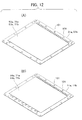
- FIG. 10 The structure of the multi-beam antenna device according to the first embodiment illustrated in FIG. 2 will be supplementarily described below. Although respective structures of the slotted plate 50 and the antenna substrate 52 are clear only from FIG. 2 , they are enlargedly illustrated in FIG. 10(A) and FIG. 10(B) , respectively.
- the plurality of slots 54 are provided in the slotted plate 50 in lengthwise and widthwise directions. Each of the slots 54 is disposed at a position approximately corresponding to a position of a respective one of the radiation elements 56 in the antenna substrate 52.
- the slotted plate 50 and the antenna substrate 52 are provided with respective ones of a pair of rivet holes 101 at positions alignable with each other when they are laminated together, and integrally riveted together with the aftermentioned other substrate, etc.
- the first ground conductor 53, the Rotman lens substrate and the second ground conductor are illustrated in FIG. 11(A), FIG. 11(B) and FIG. 11(C) , respectively.
- the first connection hole 59 and a rivet hole 101 are provided in the first ground conductor 53.
- the second connection hole 15 and a rivet hole 101 are provided in the second ground conductor 13.
- the above rivet holes serve as a means to allow the substrates and others after being laminated together to be integrally riveted.
- the metal spacer (51a, 51b) and the metal spacer (11a, 11b) are illustrated in FIG. 12(A) and FIG. 12(B) , respectively.
- An inside of each of the spacers is formed as the void (55a, 55b, 14a, 14b), or filled with the dielectric (71a, 71b).
- a rivet hole 101 provided in a peripheral portion of each of the spacers is disposed to be aligned with a rivet hole provided in other substrate or the like, when they are laminated together, to serve as a means to allow the substrates and others after being laminated together to be integrally riveted.
Abstract
Description
- The present invention relates to a design method for a Rotman lens usable in a multi-beam antenna device utilizable for millimeter band signal transmitting/receiving.
- To begin with, a conventional antenna device using a Rotman lens will be explained with its top plan view in
FIG. 8 . InFIG. 8 , the reference numeral (1) denotes a Rotman lens. The reference numerals (21),(22), --- (2m) denote respective ones of a plurality of input ports for feeding electric power, and the reference numerals (31),(32), --- (3n) denote respective ones of a plurality of output ports for extracting electric power in the Rotman lens (1). The reference numerals (41),(42), --- (4n) denote respective ones of a plurality of antenna elements for radiating electromagnetic waves to space, and the reference numeral (5) denotes an array antenna having the plurality of antenna elements (41),(42), --- (4n) arranged linearly. The reference numerals (61),(62), --- (6n) denote respective ones of a plurality of transmission lines connecting respective ones of the output ports to respective ones of the antenna elements, and the reference numeral (7) denotes a line section comprised of the transmission lines (61),(62), --- (6n) having different lengths. The reference numeral (8) denotes a center line. This antenna device is line-symmetric with respect to the center line (8). The reference numeral (9) denotes an auxiliary line for indicating a position of one (21) of the input ports. The input port (21) is located in a direction at an elevation angle α with respect to the center line (8) when viewed from S2 which is an origin of an X-Y coordinate system. The reference numeral (10) denotes a straight line which is indicative of a spatial beam direction upon excitation of the input port (21), and oriented in a direction at an angle β with respect to a direction facing a front of the array antenna. In a primitive or basic design process, a Rotman lens is generally designed under a condition of β = α. - In the conventional antenna device configured as above, when one of the input ports (21),(22), --- (2m) is excited, electric power is fed into the Rotman lens (1). The electric power in the Rotman lens (1) is extracted from each of the output ports (31),(32), --- (3n), and transmitted to a corresponding one of the antenna elements (41),(42), --- (4n) through a respective one of the transmission lines (61),(62), --- (6n). An excitation amplitude and an excitation phase of the array antenna (5) are determined by which of the input ports (21),(22), --- (2m) is excited, and the spatial beam direction is determined by the excitation phase of the array antenna (5).
- In the conventional antenna device illustrated in
FIG. 8 , the input ports (21),(22), --- (2m) are arranged on an arc having a radius R from a center located at a focal point S1 of the Rotman lens. The origin S2 of the X-Y coordinate system is represented by an intersecting point of the center line (8) with a curve segment having the output ports (31), (32), ---, (3n) arranged thereon. S3 indicates an intersecting point of the center line (8) with a curve segment having the input ports (21), (22), ---, (2m) arranged thereon. An x coordinate and a y coordinate of each of the output ports (31),(32),-(3n), and an electrical length w of each of the transmission lines (61),(62), --- (6n), are expressed in the followingFormulas 1 to 3, respectively: -


- In the
above Formulas 1 to 3,


- Further, the radius R is expressed in the following formula:

- In the
Formula 4, G is a size of the Rotman lens defined by a distance between S2 and S3. Further, F is a distance between the input port (21) and S2, and 2 Ln is an aperture length of the array antenna (5). In the basic design process, it is commonly considered that it is desirable to set η approximately in the following range: 0.8 < η < 1, i.e., set F in a range of about 1 to 1.25 times Ln, and set g to about 1.137, under a defined condition of β = α, in view of an advantage of being able to reduce an error in excitation phase at each of the output ports (31), (32), --- (3n). -
- Patent Document 1 :
JP 57-93701A - Patent Document 2:
JP 57-184305A - Patent Document 3:
JP 56-123105A - Patent Document 4:
JP 2000-124727A - However, in the conventional antenna device illustrated in
FIG. 8 , as a prerequisite to allowing the line section (7) to be configured, the radicand inside the radical symbol in the Formula 3 is required to have a positive sign or to be zero. In other words, the following Formula 5 has to be satisfied. -

- As a prerequisite to satisfying the
Formula 5, η = Ln / F has to be equal to or less than 1 (η = Ln / F ≤ 1). This means that, in cases where theaperture 2 Ln of the array antenna (5) becomes larger due to an increase in the number of the antenna elements (41),(42), --- (4n), it is necessary to increase the distance F between the input port (21) and S2 in proportion to theaperture 2 Ln of the array antenna (5), resulting in an increase in the size G of the Rotman lens. Therefore, when the number of the antenna elements (41),(42), --- (4n) is increased, it is necessary to increase the size G of the Rotman lens in conformity to an increasing rate of the antenna elements, which causes a problem that, even though the number of the antenna elements is increased, an appropriate gain enhancement effect cannot be obtained. - The present invention is directed to providing a low-loss multi-beam antenna device capable of, under a condition that β with respect to α is set to satisfy the following relation: β < α, where: β is a spatial beam-forming angle of an array antenna (5); and α is an angle between a center line (8) and a line segment which connects one of a plurality of input ports and an intersecting point S2 of the center line (8) with a curve segment having a plurality of output ports (31), (32), ---, (3n) arranged thereon, reducing G which is a size of a Rotman lens, to less than a value of G set out through a basic design process, i.e., a basic value of G when designed under a defined condition of β = α, and thereby suppressing an increase in loss of the Rotman lens so as to achieve enhanced gain.
- A multi-beam antenna of the present invention is characterized in that, under a condition that β with respect to α is set to satisfy the following relation: β < α, where: β is a spatial beam-forming angle of an array antenna; and α is an angle between a center line (8), and a line segment which connects one of a plurality of input ports and an intersecting point S2 of the center line (8) with a curve segment having a plurality of output ports (31), (32), ---, (3n) arranged thereon, a shape of a Rotman lens is set to satisfy the following relation: η=(β/α)·(Ln/F) < 1 (Formula 6), and reduce G to less than a basic value of G when designed under a defined condition of β = α, where: F is a distance between the one input port (21) and S2; 2 Ln is an aperture length of the array antenna (5); and G is a size of the Rotman lens, and defined as a distance between S2 and S3 (wherein S3 is an intersecting point of the center line (8) with a curve segment having the input ports (21), (22), ---, (2m) arranged thereon).
- In one embodiment of the present invention, the multi-beam antenna device is further characterized in that the Rotman lens is formed using a triplate.
- In one embodiment of the present invention, the multi-beam antenna device is further characterized in that the array antenna is formed using a triplate.
- In one embodiment of the present invention, the multi-beam antenna device is further characterized in that each of the input ports is partially formed as two branched transmission lines to distribute and feed electric power.
- In another aspect, a multi-beam antenna device of the present invention comprises: a Rotman lens having a plurality of input ports (21), (22), ---, (2m) for feeding electric power, and a plurality of output ports (31), (32), ---, (3n) for extracting the electric power from the input ports; an array antenna comprised of a plurality of antenna elements and adapted to radiate electromagnetic waves to space; and a plurality of transmission lines connecting respective ones of the output ports to respective ones of the antenna elements, wherein a curve for arranging the output ports thereon and a length of each of the transmission lines are set such that, when a given one of the input ports is excited, a beam is formed in a direction at an angle corresponding to that of the given input port. The multi-beam antenna device is characterized in that: β with respect to α is set to satisfy the following relation: β < α, where: β is a spatial beam-forming angle of the array antenna when viewed from a direction facing a front of the array antenna; and α is an angle between a center line (8) of the Rotman lens, and a line segment which connects one of the input ports and an intersecting point S2 of the center line (8) with a curve segment having the output ports (31), (32), ---, (3n) arranged thereon; and a shape of the Rotman lens is set to reduce G to less than a value of G when designed under a condition of β = α, where G is a size of the Rotman lens, and defined as a distance between S2 and S3 (wherein S3 is an intersecting point of the center line (8) with a curve segment having the input ports (21), (22), ---, (2m) arranged thereon).
- In yet another aspect, a multi-beam antenna device of the present invention comprises: a Rotman lens having a plurality of input ports (21), (22), ---, (2m) for feeding electric power, and a plurality of output ports (31), (32), ---, (3n) for extracting the electric power from the input ports; an array antenna comprised of a plurality of antenna elements and adapted to radiate electromagnetic waves to space; and a plurality of transmission lines connecting respective ones of the output ports to respective ones of the antenna elements, wherein a curve for arranging the output ports thereon and a length of each of the transmission lines are set such that, when a given one of the input ports is excited, a beam is formed in a direction at an angle corresponding to that of the given input port. The multi-beam antenna device is characterized in that the Rotman lens is designed according to a design procedure comprising the steps of: setting a number n of element arrays of the input or output ports; setting an arrangement pitch P of the element arrays; setting a beam number and a beam step angle; setting β with respect to α to satisfy the following relation < α, where: β is a spatial beam-forming angle of the array antenna when viewed from a direction facing a front of the array antenna; and α is an angle between a center line (8) of the Rotman lens, and a line segment which connects one of the input ports and an intersecting point S2 of the center line (8) with a curve segment having the output ports (31), (32), ---, (3n) arranged thereon; calculating Fx which allows b2 - 4ac = 0; setting a value of F; setting a value of G; and calculating respective coordinates (x, y) of the output ports of a number N corresponding to the number n of the element arrays, and a corrective line phase w in each of the output ports, whereby a shape of the Rotman lens is set to reduce G to less than a value of G when designed under a condition of β = α, where G is a size of the Rotman lens, and defined as a distance between S2 and S3 (wherein S3 is an intersecting point of the center line (8) with a curve segment having the input ports (21), (22), ---, (2m) arranged thereon). In the multi-beam antenna device,


- In still another aspect, an in-vehicle multi-beam antenna device of the present invention comprises: a Rotman lens having a plurality of input ports (21), (22), ---, (2m) for feeding electric power, and a plurality of output ports (31), (32), ---, (3n) for extracting the electric power from the input ports; an array antenna comprised of a plurality of antenna elements and each adapted to radiate electromagnetic waves to space; and a plurality of transmission lines connecting respective ones of the output ports to respective ones of the antenna elements, wherein a curve for arranging the output ports thereon and a length of each of the transmission lines are set such that, when a given one of the input ports is excited, a beam is formed in a direction at an angle corresponding to that of the given input port. The multi-beam antenna device is characterized in that β with respect to α is set to satisfy the following relation: β < α, where: β is a spatial beam-forming angle of the array antenna when viewed from a direction facing a front of the array antenna; and α is an angle between a center line (8) of the Rotman lens, and a line segment which connects one of the input ports and an intersecting point S2 of the center line (8) with a curve segment having the output ports (31), (32), ---, (3n) arranged thereon.
- The present invention can provide a low-loss multi-beam antenna device which is capable of, under a condition that β with respect to α is set to satisfy the following relation: β < α, where: β is a spatial beam-forming angle of an array antenna (5); and α is an angle between a center line (8) and a line segment which connects one of a plurality of input ports and an intersecting point S2 of the center line (8) with a curve segment having a plurality of output ports (31), (32), ---, (3n) arranged thereon, reducing G which is a size of a Rotman lens, to less than a basic value of G when designed under a defined condition of β = α, and thereby suppressing an increase in loss of the Rotman lens so as to achieve enhanced gain.
-
-
FIG. 1 is an explanatory diagram illustrating a configuration of a multi-beam antenna device according to the present invention. -
FIG. 2 is an explanatory diagram perspectively illustrating a structure of a multi-beam antenna device according to the present invention. -
FIG. 3 is an explanatory diagram illustrating a planar structure of an antenna substrate of a multi-beam antenna device according to the present invention. -
FIG. 4 is an explanatory diagram illustrating a planar structure of a Rotman lens substrate of a multi-beam antenna device according to the present invention. -
FIG. 5 is an explanatory diagram illustrating a power feeding system at input ports of a Rotman lens of a multi-beam antenna device according to the present invention. -
FIG. 6 is an explanatory diagram illustrating directivity characteristics of a multi-beam antenna device according to the present invention. -
FIG. 7 is an explanatory diagram illustrating a phase inclination in an array antenna aperture plane depending on a given input port of a multi-beam antenna device according to the present invention. -
FIG. 8 is an explanatory diagram illustrating a configuration of an example of a conventional multi-beam antenna device. -
FIG. 9A is an explanatory diagram illustrating a design flow for a Rotman lens in the conventional multi-beam antenna device. -
FIG. 9B is an explanatory diagram illustrating a design flow for a Rotman lens in a multi-beam antenna device according to the present invention. -
FIG. 10 is an explanatory diagram perspectively illustrating a part of the structure of the multi-beam antenna device according to the present invention illustrated inFIG. 2 -
FIG. 11 is an explanatory diagram perspectively illustrating a part of the structure of the multi-beam antenna device according to the present invention illustrated inFIG. 2 -
FIG. 12 is an explanatory diagram perspectively illustrating a part of the structure of the multi-beam antenna device according to the present invention illustrated inFIG. 2 - A multi-beam antenna according to the present invention is characterized in that, under a condition that β with respect to α is set to satisfy the following relation: β < α, where: β is a spatial beam-forming angle of an array antenna (5); and α is an elevation angle between a center line (8), and a line segment which connects one of a plurality of input ports and an intersecting point S2 of the center line (8) with a curve segment having a plurality of output ports (31), (32), ---, (3n) arranged thereon, a shape of a Rotman lens is set to satisfy the
Formula 6, and reduce G to less than a basic value of G when designed under a defined condition of β = α, where: F is a distance between the one input port (21) and S2; G is a size of the Rotman lens, and defined as a distance between S2 and S3; and 2 Ln is an aperture length of the array antenna (5). - Specifically, in cases where a Rotman lens is designed under the defined condition of β = α, as a prerequisite to satisfying the
Formula 5, η = Ln / F has to be equal to or less than 1 (η = Ln / F ≤1). Further, it is generally considered that it is desirable to set η approximately in the following range: 0.8 < η < 1, i.e., set F in a range of about 1 to 1.25 times Ln, and set g to about 1.137, in view of an advantage of being able to reduce an error in excitation phase at each of the output ports (31), (32), --- (3n). Thus, it is preferable to set F and G in the following respective ranges with respect to Ln:
aperture 2 Ln of the array antenna (5) becomes larger due to an increase in the number of the antenna elements (41),(42), --- (4n), the distance F between the input port (21) and S2 is increased in proportion to 2 Ln, resulting in an increase in the basic value of G. - Differently, in the present invention, for example, assuming that β = α /2, as a prerequisite to satisfying the
Formula 5, η = Ln /2 F has to be equal to or less than 1 (η = Ln / 2F ≤ 1), and it is desirable to set F in a range of about 0.5 to 0.625 times Ln, and set g to about 1.137, in view of an advantage of being able to reduce an error in excitation phase at each of the output ports (31), (32), --- (3n). Thus, desirable design can be achieved when F and G are set in the following respective ranges with respect to Ln:
In this case, the Rotman lens can be designed to have a size which is 1/2 times a basic value of G when designed under the defined condition of β = α. - In addition, in the multi-beam antenna of the present invention which is designed based on respective coordinates (x, y) of the output ports (31), (32), ---, (3n) and respective electrical lengths w of the transmission lines (61),(62), --- (6n), each calculated using the Formulas 1 to 4, when electric power is fed from a given one of the input ports which has an angle α when viewed from S2, a phase inclination of a line representing respective excitation phases at the antenna elements (41),(42), --- (4n) on the basis of that at an aperture center of the array antenna (5), as indicated by the straight line 2 in
FIG. 7 , is reduced by one-half as compared with the straight line 1 inFIG. 7 which represents respective excitation phases at the antenna elements (41),(42), --- (4n) of the basic multi-beam antenna designed under the defined condition of β = α, and a spatial beam-forming direction β of the array antenna (5) is reduced to one-half of a spatial beam-forming direction α of the array antenna (5) in the basic multi-beam antenna designed under the defined condition of β = α. - Thus, in the present invention, under the condition of β < α, a shape of the Rotman lens is set to satisfy the relation of the
Formula 6, so that it becomes possible to design a small-sized Rotman lens having a size which is β / α times a basic value of G when designed under the defined condition of β = α. This makes it possible to suppress an increase in loss of the Rotman lens which would otherwise occur in proportion to a size thereof. In addition, even if theaperture 2 Ln of the array antenna (5) becomes larger due to an increase in the number of the antenna elements (41),(42), --- (4n), and thereby the distance F between the input port (21) and S2 is increased in proportion to 2 Ln, a small-sized Rotman lens having a size reduced to β / α times the basic value of G when designed under the defined condition of β < α can be designed so as to make up a multi-beam antenna device having a spatial beam-forming direction β of the array antenna (5). - As shown in
FIG. 2 , in a multi-beam antenna device according to a first embodiment of the present invention, the Rotman lens may be formed in a triplate structure. In this case, a taper shape in complicated input and output port sections, and a phase-adjusting transmission line section (7), can be easily formed by means of etching or the like, and a first connection section (58) of the array antenna (5) and a connection port sub-section (16) of the transmission line section (7) can be electromagnetically coupled together via a first connection hole (59) provided in a first ground conductor (53). Further, in the multi-beam antenna device according to the first embodiment, the antenna array may also be formed in a triplate structure. In this case, it becomes possible to make up a low-loss multi-beam antenna device with a simple laminated structure of all components thereof. Specifically, the array antenna in the multi-beam antenna device according to the first embodiment is formed as a triplate-structured array antenna by laminating a slotted plate (50) and a feeder line (57) of an antenna substrate (52), and the first ground conductor (53) together through a dielectric (71a, 71b) interposed between adjacent ones thereof. Based on employing this structure, it becomes possible to make up a low-loss multi-beam antenna device with a simple laminated structure of all components thereof. - The above description has been made on an assumption that the present invention is applied to a commonly-used hollow parallel-plate Rotman lens, or a triplate structure in which a Rotman lens substrate (12) is supported by a dielectric having a low ε approximately equal to that of air. In a parallel plate or a triplate structure using a dielectric having a relative permittivity εr, it is apparent that the
Formula 6 in the present invention may be handled as the followingFormula 7. -

- In the multi-beam antenna device according to the first embodiment, a radiation element (56) formed in the antenna substrate (52) illustrated in
FIG. 3 can radiate an electromagnetic wave having a desired frequency in cooperation with the first ground conductor (53) and a slot (54) formed in the slot plate (50), illustrated inFIG. 2 , to serve as the antenna element. A plurality of the antenna elements are arranged to form the array antenna (5) as a whole. Further, a triplate-structured Rotman lens is made up of the first ground conductor (53), the Rotman lens substrate (12) and a second ground conductor (13), illustrated inFIG. 2 . More specifically, as illustrated inFIG. 2 , the triplate-structured Rotman lens is formed by laminating the first ground conductor (53), the transmission line section (7) of the Rotman lens substrate (12), and the second ground conductor (13) together through a dielectric (71a, 71b) interposed between adjacent ones thereof. - The first connection section (58) formed in the antenna substrate (52) is electromagnetically coupled with the connection port sub-section (16) of the transmission line section (7) formed in the Rotman lens substrate (12) illustrated in
FIG. 4 , through the first connection hole (59) formed in the first ground conductor (53), so that desired exciting electric power is transmitted from the output ports of the Rotman lens (1) to the array antenna (5). - In this process, each of a metal spacer (51a, 51b) disposed on a respective one of upper and lower sides of the antenna substrate (52) and a metal spacer (11a, 11b) disposed a respective one of upper and lower sides of the Rotman lens substrate (12) holds a respective one of the antenna substrate (52) and the Rotman lens substrate (12) in a spaced manner, while forming a metal wall around an electromagnetic coupling region between the first connection section (58) formed in the antenna substrate (52) and the connection port sub-section (16) of the transmission line section (7) formed in the Rotman lens substrate (12), so that they can contribute to efficient transmission of electric power without leakage to the surroundings, so as to achieve low-loss characteristics even at high frequencies.
- In order to stably hold the antenna substrate (52) and the Rotman lens substrate (12), each of a void (55a, 55b) in the metal spacer (51a, 51b) and a void (14a, 14b) in the metal spacers (11a, 11a) may be filled with a dielectric (71a, 71b).
- The metal spacer (11a, 11b) also forms a metal wall around the input port section (17) of the antenna device, so that it can contribute to efficient transmission of electric power to a high-frequency circuit through a second connection hole (15) formed in the second ground conductor (13) without leakage to the surroundings, so as to achieve low-loss characteristics even at high frequencies.
- Each of the first connection hole (59) and the second connection hole (15) may be formed as a waveguide opening suited to a frequency band to be used.
- In addition, based on the simple laminated structure of the components, transmission/receiving of electric power is performed by means of electromagnetic coupling, so that it is not necessary to ensure high positional accuracy during assembly at a level of conventional assembly accuracy.
- Preferably, in the multi-beam antenna device according to the first embodiment, as each of the antenna substrate (52) and the Rotman lens substrate (12), a flexible substrate prepared by laminating a polyimide film to a copper foil is employed, wherein the radiation element (56), the feeder line (57), the first connection section (58), the Rotman lens (1), the transmission line section (7), the connection port sub-section (16) of the transmission line section (7), and the input port section (17) of the antenna device, are formed by etchingly removing an unnecessary part of the copper foil.
- The flexible substrate may be prepared by employing a film as a base material and laminating a metal foil, such as a copper foil, onto the film. In this case, the radiation elements and a plurality of the feeder lines connecting therebetween may be formed by etchingly removing an unnecessary part of the copper foil (metal foil). Alternatively, the flexible substrate may be made up using a copper-cladded laminate prepared by laminating a copper foil on a thin resin sheet consisting of a glass cloth impregnated with resin. The film may be made of a material, such as polyethylene, polypropylene, polytetrafluoroethylene, ethylene fluoride-polypropylene copolymer, ethylene-tetrafluoroethylene copolymer, polyamide, polyimide, polyamide-imide, polyarylate, thermoplastic polyimide, polyetherimide, polyether ether ketone, polyethylene terephthalate, polybutylene terephthalate, polystyrene, polysulfone, polyphenylene ether, polyphenylene sulfide, or polymethylpentene. An adhesive may be used for lamination between the film and the metal foil. In view of thermal resistance, dielectric characteristics and versatility, it is preferable to use a flexible substrate prepared by laminating a polyimide film to a copper foil. In view of dielectric characteristics, a fluorine-based film is preferably used.
- As the ground conductor or the metal spacer for use in the multi-beam antenna device according to the first embodiment, a metal plate or a coated plastic plate may be used. Particularly, it is preferable to use an aluminum plate in view of an advantage of being able to produce the ground conductor or the metal spacer in a low weight and at a low cost. Alternatively, the ground conductor or the metal spacer may be made up using a flexible substrate prepared by employing a film as a base material and laminating a copper foil onto the film, or a copper-cladded laminate prepared by laminating a copper foil on a thin resin sheet consisting of a glass cloth impregnated with resin. A slot or coupling hole-forming section formed in the ground conductor may be formed by punching based on mechanical press or by etching. In view of simplicity, productivity, etc., the punching based on mechanical press is preferable.
- For example, as the substrate-supporting dielectric (71a, 71b) for use in the multi-beam antenna device according to the first embodiment, it is preferable to use a foamed material having a small relative permittivity with respect to air. The foamed material may include: a polyolefin-based foamed material such as polyethylene or polypropylene; a polystyrene-based foamed material; a polyurethane-based foamed material a polysilicone-based foamed material; and a rubber-based foamed material. Among them, a polyolefin-based foamed material is preferable, because it is lower in the relative permittivity with respect to air.
- The multi-beam antenna device according to the first embodiment will be further viewed in terms of dimensions of each member, etc., and described as a second embodiment with reference to
FIG. 2 . Each of the slotted plate (50), the first ground conductor (53), the second ground conductor (13), the metal spacer (51a, 51b), and the metal spacer (11a, 11b), is made up using an aluminum plate having a thickness of 0.3 mm. Further, the substrate-supporting dielectric (71a, 71b) is made up using a polyethylene foam having a thickness of 0.3 mm and a relative permittivity of about 1.1. Each of the antenna substrate (52) and the Rotman lens substrate (12) is made up using a flexible substrate prepared by laminating a copper foil (having a thickness, for example, of 25 µm) to a polyimide film (having a thickness, for example, of 25 µm), wherein the radiation element (56), the feeder line (57), the first connection section (58), the Rotman lens (1), the transmission line section (7), the connection port sub-section (16) of the transmission line section (7), and the input port section (17), are formed by etchingly removing an unnecessary part of the copper foil. Each of all of the ground conductors, the slotted plate and all of the metal spacers, is made up using an aluminum plate subjected to punching based on mechanical press. - In this process, each of the radiation elements (41) is formed in a square shape having a side length of 1.5 mm which is about 0.38 times a free space wavelength (λo = 3.95 mm) at a frequency of 76 GHz. Further, the slot (54) formed in the slotted plate (50) is formed in a square shape having a side length of 2.3 mm which is about 0.58 times the free space wavelength (λo = 3.95 mm) at the desired frequency of 76 GHz, and each of the first connection hole (59) formed in the first ground conductor (53) and the second connection hole (15) formed in the second ground conductor (13) is formed as a waveguide opening having a size of 1.25 mm length × 2.53 mm width. Twenty four antenna element arrays each made up of the radiation elements (56) formed in the antenna substrate (52) illustrated in
FIG. 3 , the first ground conductor (53) illustrated inFIG. 2 , the slots (54) formed in the slotted plate (50), and the feeder lines (57), are arranged at a pitch of 3.0 mm which is about 0.77 times the free space wavelength (λo = 3.95 mm) at the desired frequency of 76 GHz, to form an array antenna (5) having anantenna aperture 2 Ln of 24 × 0.77 λo as a whole. A side length is set to 2.3 mm which is about 0.58 times the free space wavelength (λo = 3.95 mm) at the desired frequency of 76 GHz. - Further, the Rotman lens (1) having the 24 output ports to be formed in the Rotman lens substrate (12) illustrated in
FIG. 4 is designed based on respective coordinates (x, y) of the output ports and respective electrical lengths w of the transmission lines calculated using theFormulas 1 to 4 on an assumption that F = 5 λo, and G = 5.7 λo, in the following range: 0.568 Ln < G < 0.71 Ln, while satisfying theFormula 6 wherein β = α / 2, i.e., a condition of η = (1 / 2) · (Ln / F) < 1. Specifically, the size G of the Rotman lens (1) is set to a value which is about 5.7 times the free space wavelength (λo = 3.95 mm) at the desired frequency of 76 GHz, i.e., to 22.5 mm. - The above members were actually laminated in order as illustrated in
FIG. 2 to make up a multi-beam antenna device, and a measurement unit was connected to the multi-beam antenna device to measure characteristics thereof. As a result, a reflectance loss of each of the following eight input ports was equal to or less than - 15dB, and a gain directionality corresponding to each of the eight input ports was obtained as shown inFIG. 6 . Further, it could be ascertained that a beam of the array antenna (5) can be formed in a direction at an angle β which is about one-half of an input port angle α, as shown in Table 1. In this case, an insertion loss of the Rotman lens (1) having the size G = 22.5 mm was about 2.5 dB.TABLE 1 Input Port No. Input Port
Angle α (degree)Antenna Beam
Angle β (degree)1 26 13.0 2 19 9.4 3 12 5.9 4 5 2.3 5 - 5 -2.0 6 - 12 - 5.5 7 -19 - 9.2 8 -26 - 12.7 - On the other hand, in a conventional Rotman lens designed in the following range: 1.137 Ln < G < 1.42 Ln, while satisfying the condition of the
Formula 5 under the defined condition of β=α, i.e., η = Ln / F < 1, it is at least necessary that G = 1.137, Ln = 10.5 λo, so that the size G of the conventional Rotman lens is set to a value which is about 10.5 times the free space wavelength (λo = 3.95 mm) at the desired frequency of 76 GHz, i.e., to 41.5 mm. In this case, an insertion loss of the Rotman lens (1) was about 5 dB. - As above, the multi-beam antenna device according to the second embodiment is improved in relative gain by 2.5 dB or more, in comparison on the basis of a loss in a multi-beam antenna device formed by the conventional design process, so that it can achieve excellent characteristics.
- In a multi-beam antenna device according to a third embodiment, as shown in
FIG. 5 , a connection portion of each of a plurality of input ports (521),(522), --- (52m) is formed as a two branched transmission lines to distribute and feed electric power, which allows the electric power fed from the input ports into a Rotman lens (1) to be concentrated in a central region of a plurality of output ports (531),(532), --- (53n), so as to suppress dispersion of the electric power toward a region devoid of the output ports (531),(532), --- (53n) in a curve segment having the output ports arranged thereon. This makes it possible to reduce an unnecessary internal reflection component to suppress deterioration in sidelobe characteristics of radiation beams of an array antenna (5). Particularly, when electric power is input from an input port, such as the input port (521) or the input port (52n), located at an end of the curve segment having the input ports arranged thereon, electric power may be fed while setting a phase difference between the two branched transmission lines of the connection portion. This makes it possible to control a propagation direction of the electric power fed into the Rotman lens (1) in such a manner as to concentrate the electric power in the central region of the output ports (531),(532), --- (53n), to suppress deterioration in sidelobe characteristics of radiation beams of the array antenna (5). The above function never impairs the advantageous effects as shown inFIG. 6 but rather generates a synergistic effect. - As mentioned in the "Background Art", design of a lens based on the Rotman's concept is generally performed under the condition of β = α. One feature of the present invention is that the present invention makes it possible to design a Rotman lens under the condition of β < α, using the aforementioned modified Rotman process based on the conventional Rotman lens design process. Specifically, under the condition of β <α, β (radiation angle on the side of the antenna elements) is less than α (beam angle on the side of the Rotman lens). Thus, the present invention is effective, particularly, when it a high resolution is required with respect to a narrow angle. For example, in cases where the multi-beam antenna device according to the present invention is mounted in a vehicle, it can realize a detection capability sensitive to a range of about 15 degrees in each of rightward and leftward directions with respect to 0 degree defined by a direction perpendicular to a frontward-rearward direction of the vehicle (i.e., it has an aperture angle of up to about 30 degrees as a total of the rightward and leftward angles).
In other words, the antenna device according to the present invention can obtain ideal electric power and phase distributions required for an in-vehicle antenna device or the like. - There is a conventional technique (the Patent Document 3) where lens design is performed under a condition of β > α, instead of β < α as in the present invention. Just to make sure, the
Patent Document 3 will be mentioned below. The invention described in thePatent Document 3 is an antenna device which comprise parallel plates having a plurality of input elements adapted to be excited individually so as to feed electric power, and a plurality of output elements adapted to extract the electric power; and a transmission line for connection with an array antenna comprised of a plurality of antenna elements and adapted to radiate electromagnetic waves to space, wherein a curve for arranging the output elements thereon, and a length of the transmission line, are set based on three focal points on a curve for arranging the input elements thereon, in such a manner that, when a given one of the input elements is excited, a beam is radiated in a direction at an angle corresponding to that of the given input port, and wherein a shape of the curve for arranging the input elements thereon is not a part of a circle. - As can be understood from the above, due to the lens design performed under the condition of β > α (see
FIG. 2 in the Patent Document 3), the shape of the curve for arranging the input elements thereon is set so as not to become a part of a circle, which shows that this antenna device is designed based on a process totally different from the Rotman's design process.
Considering the invention described in thePatent Document 3, an application having a need to set β (radiation angle on the side of the antenna elements) to be greater than α (beam angle on the side of the Rotman lens) would include a military radar operable to detect a wide angular range with a less phase error. - Thus, the antenna device according to the present invention and the antenna device described in the
patent Document 3 are totally different from each other in terms of a configuration (lens shape) and a problem to be solved (object). - The
Patent Document 4 filed by the applicant of this application will also be mentioned below. ThePatent Document 4 describes a beam-scanning planar antenna excellent in thinning and simplification of an assembling process and capable of facilitating a reduction in size. The planar antenna comprises a connection module 104 for connection with a system, a Rotman lens module 103, and a beam-scan antenna module 102, which are laminated in this order, wherein the planar antenna is formed by laminating: athird ground conductor 13; a fourth dielectric 34; aRotman lens substrate 62 having a Rotman lens pattern, asecond connection section 52 and a third connection section 92; a third dielectric 33; asecond ground conductor 12; asecond dielectric 32; afeeder substrate 61 formed with a plurality of antenna groups each comprising a combination of aradiation element 50, a feeder line 40 and a first connection section 51; afirst dielectric 31; and a first ground conductor 11, in this order.
Design of the Rotman lens of this beam-scanning planar antenna is performer under the condition of α = β as with the conventional technique, and the number of elements in the planar antenna described in thePatent Document 4 is less than the number of elements in the present invention, as can be understood from directivity characteristics inFIG. 2 of thePatent Document 4. Thus, if theaperture 2 Ln of the array antenna becomes larger due to an increase in the number of the antenna elements, it is necessary to increase the distance F between the input port and S2 in proportion to theaperture 2 Ln of the array antenna (5), which causes a problem of an increase in the size G of the Rotman lens, as mentioned above. Therefore, the present invention is intended to solve this problem, and provides a low-loss multi-beam antenna device capable of designing a Rotman lens to suppress an increase in loss so as to achieve enhanced gain. - One feature of the present invention is that the present invention makes it possible to design a Rotman lens under the condition of β < α, using the aforementioned modified Rotman process based on the conventional Rotman lens design process. This modified Rotman process will be more specifically described based on the flowcharts illustrated in
FIGS. 9A and9B . -
FIG. 9A is a design flow based on the conventional Rotman process. Upon start of the design flow in S901, the process advances to S902, wherein a number n of antenna element arrays is set. Then, the process advances to S903, wherein an arrangement pitch P of the n antenna element arrays is set. Thus, theantenna aperture 2 Ln is expressed as follows: 2 Ln = (n ---- 1) P. Then, the process advances to S904, wherein a beam number and a beam step angle are set. The beam number means the number of input ports. The beam step angle means an angular difference between the antenna beam angle β and each of the input port Nos. (For example, in Table 1, the beam step angle is around about 4 degrees) Then, the process advances to S905, wherein F0 which allows b2- 4ac = 0 is calculated. - In the conventional Rotman process, the design is performed under the condition of α = β, and thereby F0 = Ln. Further, Fx = β · F0/ 1. Thus, under the condition of α> β as in the present invention, it is obvious that Fx becomes less than F0 (Fx < F0). Thus, under the condition of α = β, in Fx, η = Ln / F becomes less than 1 (η = Ln / F ≤ 1). In this case, b2 - 4ac in the
Formula 5 has a negative value, which means that the design fails. - Then, in S906, the distance F between the input port (21) and S2 is set. In this case, the distance F is set in the following range: F0 < F < 1.25 F0. Then, the process advances to S907, wherein the lens size G is set. In this case, the size G is set in the following range: g F0 < G < 1.25 g F0. Specifically, when the shape factor g = G/F is set to a typical value of 1.136, the size G is set in the following range: 1.136 F0 < G < 1.4 F0.
- Then, in S908, respective coordinates (x, y) of the output ports of a number n corresponding to the number n of the element arrays, and a corrective line phase w in each of the output ports, are calculated.
-
FIG. 9A is a design flow based on the modified Rotman process in the present invention. A difference fromFIG. 9A is that a ratio of β to α can be set in S915, wherein the ratio can be set to satisfy the following relationship: α > β. The ratio set in this manner is used as a coefficient or factor for η, as indicated in theFormula 6. Specifically, respective coordinates (x, y) of the ports are calculated while controlling each design parameter to satisfy the following relation:
- Based on the above difference, the design flow based on the modified Rotman process in the present invention is configured as follows. Upon start of the design flow in S911, the process advances to S912, wherein a number n of antenna element arrays is set. Then, the process advances to S913, wherein an arrangement pitch P of the n antenna element arrays is set. Then, the process advances to S914, wherein a beam number and a beam step angle are set. Then, in S915, a ratio of β to α can be set to satisfy the following relationship: α > β, as mentioned above. Then, the process advances to S916, wherein Fx which allows b2 - 4ac = 0 is calculated. Under the condition of α > β, Fx=β · Ln/ α. Then, in S917, the distance F between the input port (21) and S2 is set. In this case, the distance F is set in the following range: Fx < F < 1.25 Fx. Then, the process advances to S918, wherein the lens size G is set. In this case, the size G is set in the following range: g Fx < G < 1.25 g Fx. Specifically, when the shape factor g = G/F is set to a typical value of 1.136, the size G is set in the following range: 1.136 Fx < G < 1.4 Fx.
- Then, in S919, respective coordinates (x, y) of the output ports of a number n corresponding to the number n of the element arrays, and a corrective line phase w in each of the output ports, are calculated.
- The first and second embodiments have been described together with specific numerical values under the following condition represented by the Formula 6: η = (β/α)·(Ln/F) < 1 (6). Some supplemental explanation will be added here. In a preferred embodiment, β / α is approximately in the following numerical range;

- An upper limit value of η is assumed as η = (β / α) · (Ln / F) ≈ 1. In this case, F is minimized (minimum value in a selection range of F).
- A standard value of η is assumed as η = (β / α) · (Ln / F) = 0.88. In this case, F is optimized (optimal value in the selection range of F).
- A lower limit value of η is assumed as η = (β / α) · (Ln / F) ≤ 0.5 to 0.7. In this case, F is maximized (maximum value in the selection range of F).
An actual value of F measured when η has an upper limit value, a standard value or a lower limit value, is expresses as multiples of wave length λ, and summarized in the following Table 2.TABLE 2 First Embodiment η: Upper Limit η: Standard η: Lower Limit Ratio β/α Number of Element Arrays Arrangement Pitch (η ≈ 1)
F min(η = 0.88)
F optimalF max 0.7 24 0.77λ 6.5λ 7λ 9λ
η = 0.670.5 24 0.77λ 4.5λ 5λ 9λ
η = 0.50.33 24 0.77λ 3λ 3.3λ 6λ
η = 0.5
2 Ln (= (n - 1) P) means an aperture length of the array antenna (5), and indicates a distance between one (a central one) of the radiation elements (56) in one of the element arrays on one side of the antenna substrate (52), and one (a central one) of the radiation elements (56) in one of the element arrays on the other side of the antenna substrate (52).
The angle β indicates an angle between a perpendicular line extending from the radiation element (56) toward the slotted plate, and a direction along which a beam is radiated from the radiation element.
In the present invention, in cases where a Rotman lens is designed from preset input port coordinates (x, y), and output port coordinates (x, y) calculated based on theFormulas
A level of reduction in G in the present invention as compared to G in the conventional technique will be described below.
G1 in the present invention with respect to G0 in the conventional technique can be technically achieved in the following range: 0.25 G0 < G1 < 0.80 G0. Based on Table 2, the following range would be derived using the aforementioned Formulas: 0.33 G0 < G1 < 0.67 G0. Further, it is noted that a significantly excellent result is actually obtained in the following range: 0.33 G0 < G1 < 0.5 G0. - In the same way, an actual measurement result corresponding to the third embodiment is summarized in the following Table 3.
TABLE 3 Third Embodiment η: Upper Limit η: Standard η: Lower Limit Ratio β/α Number of Element Arrays Arrangement Pitch (η ≈ 1)
F min(η = 0.88)
F optimalF max 0.7 16 0.77λ 4.1λ 4.5λ 6λ
η = 0.760.5 16 0.77λ 2.9λ 3.3λ 6λ
η = 0.50.33 16 0.77λ 2λ 2.2λ 3.8λ
η = 0.5 - The structure of the multi-beam antenna device according to the first embodiment illustrated in
FIG. 2 will be supplementarily described below. Although respective structures of the slottedplate 50 and theantenna substrate 52 are clear only fromFIG. 2 , they are enlargedly illustrated inFIG. 10(A) and FIG. 10(B) , respectively. InFIG. 10 , the plurality ofslots 54 are provided in the slottedplate 50 in lengthwise and widthwise directions. Each of theslots 54 is disposed at a position approximately corresponding to a position of a respective one of theradiation elements 56 in theantenna substrate 52. Further, the slottedplate 50 and theantenna substrate 52 are provided with respective ones of a pair of rivet holes 101 at positions alignable with each other when they are laminated together, and integrally riveted together with the aftermentioned other substrate, etc.
Thefirst ground conductor 53, the Rotman lens substrate and the second ground conductor are illustrated inFIG. 11(A), FIG. 11(B) and FIG. 11(C) , respectively. InFIG. 11 , thefirst connection hole 59 and arivet hole 101 are provided in thefirst ground conductor 53. Thesecond connection hole 15 and arivet hole 101 are provided in thesecond ground conductor 13. The above rivet holes serve as a means to allow the substrates and others after being laminated together to be integrally riveted.
The metal spacer (51a, 51b) and the metal spacer (11a, 11b) are illustrated inFIG. 12(A) and FIG. 12(B) , respectively. An inside of each of the spacers is formed as the void (55a, 55b, 14a, 14b), or filled with the dielectric (71a, 71b). Arivet hole 101 provided in a peripheral portion of each of the spacers is disposed to be aligned with a rivet hole provided in other substrate or the like, when they are laminated together, to serve as a means to allow the substrates and others after being laminated together to be integrally riveted. -
- 1: Rotman lens
- 5: array antenna
- 7: transmission line section
- 8: center line of Rotman lens
- 9: auxiliary line for indicating position of input port
- 10: beam direction when viewed from a direction facing array antenna
- 11a, 11b: metal spacer
- 12: Rotman lens substrate
- 13: second ground conductor
- 14a, 14b: void
- 15: second connection hole
- 16: connection port sub-section of transmission line section
- 17: input port section of multi-beam antenna device
- 21, 22, --- 2m: Rotman lens input port
- 31, 32, --- 3n: Rotman lens output port
- 41, 42, --- 4n: antenna element
- 50: slotted plate
- 51a, 51b: metal spacer
- 52: antenna substrate
- 53: first ground conductor
- 54: slot
- 55a, 55b: void
- 56: radiation element
- 57: feeder line
- 58: first connection section
- 59: first connection hole
- 61, 62, --- 6n: transmission line connecting output port to antenna element
- 71a, 71b: substrate-supporting dielectric
Claims (13)
- A multi-beam antenna device comprising: a Rotman lens having a plurality of input ports (21), (22), ---, (2m) for feeding electric power, and a plurality of output ports (31), (32), ---, (3n) for extracting the electric power from the input ports; an array antenna comprised of a plurality of antenna elements and adapted to radiate electromagnetic waves to space; and a plurality of transmission lines connecting respective ones of the output ports to respective ones of the antenna elements, wherein a curve for arranging the output ports thereon and a length of each of the transmission lines are set such that, when a given one of the input ports is excited, a beam is formed in a direction at an angle corresponding to that of the given input port, characterized in that:β with respect to α is set to satisfy the following relation: β < α, where: β is a spatial beam-forming angle of the array antenna when viewed from a direction facing a front of the array antenna; and α is an angle between a center line (8) of the Rotman lens, and a line segment which connects one of the input ports and an intersecting point S2 of the center line (8) with a curve segment having the output ports (31), (32), ---, (3n) arranged thereon; anda shape of the Rotman lens is set to satisfy the following relation: η=(β/α)·(Ln/F) < 1, and reduce G to less than a value of G when designed under a condition of β = α, where: F is a distance between the one input port (21) and S2; 2 Ln is an aperture length of the array antenna; and G is a size of the Rotman lens, and defined as a distance between S2 and S3 (wherein S3 is an intersecting point of the center line (8) with a curve segment having the input ports (21), (22), ---, (2m) arranged thereon); and 2 Ln is an aperture length of the array antenna.
- The multi-beam antenna device as defined in claim 1, characterized in that the Rotman lens is formed using a triplate.
- The multi-beam antenna device as defined in claim 2, characterized in that the array antenna is formed using a triplate.
- The multi-beam antenna device as defined in any one of claims 1 to 3, characterized in that each of the input ports is partially formed as two branched transmission lines to distribute and feed electric power.
- A multi-beam antenna device comprising: a Rotman lens having a plurality of input ports (21), (22), ---, (2m) for feeding electric power, and a plurality of output ports (31), (32), ---, (3n) for extracting the electric power from the input ports; an array antenna comprised of a plurality of antenna elements and adapted to radiate electromagnetic waves to space; and a plurality of transmission lines connecting respective ones of the output ports to respective ones of the antenna elements, wherein a curve for arranging the output ports thereon and a length of each of the transmission lines are set such that, when a given one of the input ports is excited, a beam is formed in a direction at an angle corresponding to that of the given input port, characterized in that:β with respect to α is set to satisfy the following relation: β < α, where: β is a spatial beam-forming angle of the array antenna when viewed from a direction facing a front of the array antenna; and α is an angle between a center line (8) of the Rotman lens, and a line segment which connects one of the input ports and an intersecting point S2 of the center line (8) with a curve segment having the output ports (31), (32), ---, (3n) arranged thereon; anda shape of the Rotman lens is set to reduce G to less than a value of G when designed under a condition of β = α, where G is a size of the Rotman lens, and defined as a distance between S2 and S3 (wherein S3 is an intersecting point of the center line (8) with a curve segment having the input ports (21), (22), ---, (2m) arranged thereon).
- The multi-beam antenna device as defined in claim 5, characterized in that the Rotman lens is formed using a triplate.
- The multi-beam antenna device as defined in claim 6, characterized in that the array antenna is formed using a triplate.
- The multi-beam antenna device as defined in any one of claims 5 to 7, characterized in that each of the input ports is partially formed as two branched transmission lines to distribute and feed electric power.
- A multi-beam antenna device comprising: a Rotman lens having a plurality of input ports (21), (22), ---, (2m) for feeding electric power, and a plurality of output ports (31), (32), ---, (3n) for extracting the electric power from the input ports; an array antenna comprised of a plurality of antenna elements and adapted to radiate electromagnetic waves to space; and a plurality of transmission lines connecting respective ones of the output ports to respective ones of the antenna elements, wherein a curve for arranging the output ports thereon and a length of each of the transmission lines are set such that, when a given one of the input ports is excited, a beam is formed in a direction at an angle corresponding to that of the given input port, characterized in that the Rotman lens is designed according to a design procedure comprising the steps of:setting a number n of element arrays of the input or output ports;setting an arrangement pitch P of the element arrays;setting a beam number and a beam step angle;setting β with respect to α to satisfy the following relation: β < α, where: β is a spatial beam-forming angle of the array antenna when viewed from a direction facing a front of the array antenna; and α is an angle between a center line (8) of the Rotman lens, and a line segment which connects one of the input ports and an intersecting point S2 of the center line (8) with a curve segment having the output ports (31), (32), ---, (3n) arranged thereon;calculating Fx which allows b2 - 4ac = 0;setting a value of F;setting a value of G; andcalculating respective coordinates (x, y) of the output ports of a number N corresponding to the number n of the element arrays, and a corrective line phase w in each of the output ports,whereby a shape of the Rotman lens is set to reduce G to less than a value of G when designed under a condition of β = α, where G is a size of the Rotman lens, and defined as a distance between S2 and S3 (wherein S3 is an intersecting point of the center line (8) with a curve segment having the input ports (21), (22), ---, (2m) arranged thereon),wherein

 where
where
- An in-vehicle multi-beam antenna device comprising: a Rotman lens having a plurality of input ports (21), (22), ---, (2m) for feeding electric power, and a plurality of output ports (31), (32), ---, (3n) for extracting the electric power from the input ports; an array antenna comprised of a plurality of antenna elements and each adapted to radiate electromagnetic waves to space; and a plurality of transmission lines connecting respective ones of the output ports to respective ones of the antenna elements, wherein a curve for arranging the output ports thereon and a length of each of the transmission lines are set such that, when a given one of the input ports is excited, a beam is formed in a direction at an angle corresponding to that of the given input port, characterized in that β with respect to α is set to satisfy the following relation, β < α, where: β is a spatial beam-forming angle of the array antenna when viewed from a direction facing a front of the array antenna; and α is an angle between a center line (8) of the Rotman lens, and a line segment which connects one of the input ports and an intersecting point S2 of the center line (8) with a curve segment having the output ports (31), (32), ---, (3n) arranged thereon.
- The in-vehicle multi-beam antenna device as defined in claim 10, characterized in that the Rotman lens is formed using a triplate.
- The in-vehicle multi-beam antenna device as defined in claim 11, characterized in that the array antenna is formed using a triplate.
- The multi-beam antenna device as defined in any one of claims 10 to 12, characterized in that each of the input ports is partially formed as two branched transmission lines to distribute and feed electric power.
Applications Claiming Priority (2)
| Application Number | Priority Date | Filing Date | Title |
|---|---|---|---|
| JP2008303781 | 2008-11-28 | ||
| PCT/JP2009/070108 WO2010061948A1 (en) | 2008-11-28 | 2009-11-30 | Multibeam antenna device |
Publications (2)
| Publication Number | Publication Date |
|---|---|
| EP2372835A1 true EP2372835A1 (en) | 2011-10-05 |
| EP2372835A4 EP2372835A4 (en) | 2015-06-17 |
Family
ID=42225810
Family Applications (1)
| Application Number | Title | Priority Date | Filing Date |
|---|---|---|---|
| EP09829186.7A Ceased EP2372835A4 (en) | 2008-11-28 | 2009-11-30 | Multibeam antenna device |
Country Status (6)
| Country | Link |
|---|---|
| US (1) | US8698689B2 (en) |
| EP (1) | EP2372835A4 (en) |
| JP (1) | JP5838465B2 (en) |
| KR (1) | KR101266698B1 (en) |
| CN (1) | CN102301527B (en) |
| WO (1) | WO2010061948A1 (en) |
Cited By (1)
| Publication number | Priority date | Publication date | Assignee | Title |
|---|---|---|---|---|
| US11322816B2 (en) | 2017-06-26 | 2022-05-03 | Huawei Technologies Co., Ltd. | Feeding device |
Families Citing this family (15)
| Publication number | Priority date | Publication date | Assignee | Title |
|---|---|---|---|---|
| US8866691B2 (en) * | 2007-04-20 | 2014-10-21 | Skycross, Inc. | Multimode antenna structure |
| EP2624475B1 (en) * | 2012-01-31 | 2015-01-28 | Fraunhofer-Gesellschaft zur Förderung der angewandten Forschung e.V. | Combined Power Transmission |
| JP6003811B2 (en) * | 2013-06-05 | 2016-10-05 | 日立金属株式会社 | Antenna device |
| US9780457B2 (en) * | 2013-09-09 | 2017-10-03 | Commscope Technologies Llc | Multi-beam antenna with modular luneburg lens and method of lens manufacture |
| US9368870B2 (en) * | 2014-03-17 | 2016-06-14 | Ubiquiti Networks, Inc. | Methods of operating an access point using a plurality of directional beams |
| CN104319466A (en) * | 2014-09-25 | 2015-01-28 | 东南大学 | Multi-beam scanning antenna |
| KR102435550B1 (en) * | 2015-06-09 | 2022-08-24 | 주식회사 에이치엘클레무브 | Apparatur for processing signal of radar and method for processing signal thereof |
| US11329393B2 (en) * | 2016-12-07 | 2022-05-10 | Fujikura Ltd. | Antenna device |
| US10230166B2 (en) * | 2017-04-18 | 2019-03-12 | The Boeing Company | Plasma switched array antenna |
| CN108172998A (en) * | 2017-12-21 | 2018-06-15 | 四川中测微格科技有限公司 | A kind of structure for improving Wave-packet shaping network device interface isolation |
| CN108562876A (en) * | 2018-01-31 | 2018-09-21 | 中国电子科技集团公司第三十八研究所 | Broadband low minor lobe simulates multiple-beam array reconnaissance system |
| JP7152190B2 (en) * | 2018-05-28 | 2022-10-12 | 矢崎総業株式会社 | Detection equipment and detection system |
| KR102129897B1 (en) * | 2019-06-12 | 2020-07-03 | 조선대학교산학협력단 | Beam tilting antenna apparatus with variable beam width |
| WO2021231725A1 (en) * | 2020-05-14 | 2021-11-18 | The Regents Of The University Of California | Parametric flat lenses for near-field imaging and electronic beam scanning |
| CN114512824B (en) * | 2022-03-11 | 2023-10-24 | 电子科技大学 | Millimeter wave cross scanning multibeam array antenna based on common cavity rotman lens |
Family Cites Families (13)
| Publication number | Priority date | Publication date | Assignee | Title |
|---|---|---|---|---|
| JPS56123105A (en) | 1980-03-04 | 1981-09-28 | Tech Res & Dev Inst Of Japan Def Agency | Antenna device |
| JPS5793701A (en) | 1980-12-03 | 1982-06-10 | Mitsubishi Electric Corp | Antenna device |
| JPS57184305A (en) * | 1981-05-09 | 1982-11-13 | Mitsubishi Electric Corp | Antenna device |
| JP4089043B2 (en) | 1998-10-20 | 2008-05-21 | 日立化成工業株式会社 | Planar antenna for beam scanning |
| DE19951123C2 (en) * | 1999-07-30 | 2003-11-13 | Volkswagen Ag | Radar sensor for monitoring the surroundings of a motor vehicle |
| KR100486831B1 (en) * | 2000-04-18 | 2005-04-29 | 히다치 가세고교 가부시끼가이샤 | Planar antenna for beam scanning |
| US6480167B2 (en) * | 2001-03-08 | 2002-11-12 | Gabriel Electronics Incorporated | Flat panel array antenna |
| JP2003152422A (en) * | 2001-11-19 | 2003-05-23 | Mitsubishi Electric Corp | Antenna array device |
| JP2007189596A (en) * | 2006-01-16 | 2007-07-26 | Nippon Hoso Kyokai <Nhk> | Beam forming device |
| US7724197B1 (en) * | 2007-04-30 | 2010-05-25 | Planet Earth Communications, Llc | Waveguide beam forming lens with per-port power dividers |
| JP5146138B2 (en) * | 2008-06-19 | 2013-02-20 | 富士通株式会社 | Wireless communication apparatus and transmission beam control method |
| EP2393156B1 (en) * | 2009-01-29 | 2014-12-03 | Hitachi Chemical Company, Ltd. | Multi-beam antenna apparatus |
| JP2012222523A (en) * | 2011-04-06 | 2012-11-12 | Hitachi Chem Co Ltd | Antenna scanning device and radio communication system using the same |
-
2009
- 2009-11-30 US US13/131,752 patent/US8698689B2/en active Active
- 2009-11-30 WO PCT/JP2009/070108 patent/WO2010061948A1/en active Application Filing
- 2009-11-30 KR KR1020117014799A patent/KR101266698B1/en active IP Right Grant
- 2009-11-30 CN CN200980155542.3A patent/CN102301527B/en active Active
- 2009-11-30 EP EP09829186.7A patent/EP2372835A4/en not_active Ceased
- 2009-11-30 JP JP2009271889A patent/JP5838465B2/en active Active
Non-Patent Citations (1)
| Title |
|---|
| See references of WO2010061948A1 * |
Cited By (1)
| Publication number | Priority date | Publication date | Assignee | Title |
|---|---|---|---|---|
| US11322816B2 (en) | 2017-06-26 | 2022-05-03 | Huawei Technologies Co., Ltd. | Feeding device |
Also Published As
| Publication number | Publication date |
|---|---|
| KR101266698B1 (en) | 2013-05-28 |
| US8698689B2 (en) | 2014-04-15 |
| WO2010061948A1 (en) | 2010-06-03 |
| CN102301527A (en) | 2011-12-28 |
| JP5838465B2 (en) | 2016-01-06 |
| KR20110091023A (en) | 2011-08-10 |
| CN102301527B (en) | 2015-06-24 |
| JP2010154522A (en) | 2010-07-08 |
| EP2372835A4 (en) | 2015-06-17 |
| US20110241968A1 (en) | 2011-10-06 |
Similar Documents
| Publication | Publication Date | Title |
|---|---|---|
| EP2372835A1 (en) | Multibeam antenna device | |
| EP2393156B1 (en) | Multi-beam antenna apparatus | |
| EP2575210B1 (en) | Variable height radiating aperture | |
| JP4803172B2 (en) | Planar antenna module, triplate type planar array antenna, and triplate line-waveguide converter | |
| EP2293380B1 (en) | Triplate line inter-layer connector, and planar array antenna | |
| CA2828089C (en) | Structural wideband multifunctional apertures | |
| EP2575213B1 (en) | Co-phased, dual polarized antenna array with broadband and wide scan capability | |
| EP2136433A1 (en) | Triplate line/waveguide converter | |
| US9190727B1 (en) | Structural wideband multifunctional aperture manufacturing | |
| EP1671398B1 (en) | Dual polarised antenna array and method for manufacturing the same | |
| US6720931B1 (en) | Planar antenna for beam scanning | |
| US10826148B2 (en) | Ridge waveguide and array antenna apparatus | |
| EP2664029B1 (en) | Printed circuit board based feed horn | |
| Nematollahi et al. | Realization of focused beam and shaped beam transmitarrays based on broadband unit cells | |
| JP5288330B2 (en) | Planar array antenna | |
| KR101863311B1 (en) | Antenna substrate used interrogator antenna of identification of friend or foe | |
| WO2018074056A1 (en) | Antenna device | |
| US20230420859A1 (en) | Conformal and flexible leaky-wave antenna arrays with reduced mutual couplings | |
| Wang | Advanced transmitarrays and their beam scanning for future wireless communications | |
| KR101863312B1 (en) | Antenna substrate used interrogator antenna of identification of friend or foe | |
| Bakan | A low-profile wideband antenna array with wide-scan ability |
Legal Events
| Date | Code | Title | Description |
|---|---|---|---|
| PUAI | Public reference made under article 153(3) epc to a published international application that has entered the european phase |
Free format text: ORIGINAL CODE: 0009012 |
|
| 17P | Request for examination filed |
Effective date: 20110628 |
|
| AK | Designated contracting states |
Kind code of ref document: A1 Designated state(s): AT BE BG CH CY CZ DE DK EE ES FI FR GB GR HR HU IE IS IT LI LT LU LV MC MK MT NL NO PL PT RO SE SI SK SM TR |
|
| DAX | Request for extension of the european patent (deleted) | ||
| RA4 | Supplementary search report drawn up and despatched (corrected) |
Effective date: 20150520 |
|
| RIC1 | Information provided on ipc code assigned before grant |
Ipc: H01Q 21/06 20060101ALI20150513BHEP Ipc: H01Q 3/26 20060101AFI20150513BHEP |
|
| 17Q | First examination report despatched |
Effective date: 20160321 |
|
| STAA | Information on the status of an ep patent application or granted ep patent |
Free format text: STATUS: EXAMINATION IS IN PROGRESS |
|
| STAA | Information on the status of an ep patent application or granted ep patent |
Free format text: STATUS: EXAMINATION IS IN PROGRESS |
|
| APBK | Appeal reference recorded |
Free format text: ORIGINAL CODE: EPIDOSNREFNE |
|
| APBN | Date of receipt of notice of appeal recorded |
Free format text: ORIGINAL CODE: EPIDOSNNOA2E |
|
| APBR | Date of receipt of statement of grounds of appeal recorded |
Free format text: ORIGINAL CODE: EPIDOSNNOA3E |
|
| APAV | Appeal reference deleted |
Free format text: ORIGINAL CODE: EPIDOSDREFNE |
|
| APBX | Invitation to file observations in appeal sent |
Free format text: ORIGINAL CODE: EPIDOSNOBA2E |
|
| REG | Reference to a national code |
Ref country code: DE Ref legal event code: R003 |
|
| APBT | Appeal procedure closed |
Free format text: ORIGINAL CODE: EPIDOSNNOA9E |
|
| STAA | Information on the status of an ep patent application or granted ep patent |
Free format text: STATUS: THE APPLICATION HAS BEEN REFUSED |
|
| 18R | Application refused |
Effective date: 20221025 |