EP2372793B1 - LED package mounting structure - Google Patents
LED package mounting structure Download PDFInfo
- Publication number
- EP2372793B1 EP2372793B1 EP10014139A EP10014139A EP2372793B1 EP 2372793 B1 EP2372793 B1 EP 2372793B1 EP 10014139 A EP10014139 A EP 10014139A EP 10014139 A EP10014139 A EP 10014139A EP 2372793 B1 EP2372793 B1 EP 2372793B1
- Authority
- EP
- European Patent Office
- Prior art keywords
- led package
- circuit board
- solder
- package
- mounting structure
- Prior art date
- Legal status (The legal status is an assumption and is not a legal conclusion. Google has not performed a legal analysis and makes no representation as to the accuracy of the status listed.)
- Not-in-force
Links
Images


Classifications
-
- H—ELECTRICITY
- H05—ELECTRIC TECHNIQUES NOT OTHERWISE PROVIDED FOR
- H05K—PRINTED CIRCUITS; CASINGS OR CONSTRUCTIONAL DETAILS OF ELECTRIC APPARATUS; MANUFACTURE OF ASSEMBLAGES OF ELECTRICAL COMPONENTS
- H05K3/00—Apparatus or processes for manufacturing printed circuits
- H05K3/30—Assembling printed circuits with electric components, e.g. with resistors
- H05K3/32—Assembling printed circuits with electric components, e.g. with resistors electrically connecting electric components or wires to printed circuits
- H05K3/34—Assembling printed circuits with electric components, e.g. with resistors electrically connecting electric components or wires to printed circuits by soldering
- H05K3/341—Surface mounted components
- H05K3/3431—Leadless components
- H05K3/3442—Leadless components having edge contacts, e.g. leadless chip capacitors, chip carriers
-
- H—ELECTRICITY
- H05—ELECTRIC TECHNIQUES NOT OTHERWISE PROVIDED FOR
- H05K—PRINTED CIRCUITS; CASINGS OR CONSTRUCTIONAL DETAILS OF ELECTRIC APPARATUS; MANUFACTURE OF ASSEMBLAGES OF ELECTRICAL COMPONENTS
- H05K2201/00—Indexing scheme relating to printed circuits covered by H05K1/00
- H05K2201/09—Shape and layout
- H05K2201/09209—Shape and layout details of conductors
- H05K2201/09372—Pads and lands
- H05K2201/09472—Recessed pad for surface mounting; Recessed electrode of component
-
- H—ELECTRICITY
- H05—ELECTRIC TECHNIQUES NOT OTHERWISE PROVIDED FOR
- H05K—PRINTED CIRCUITS; CASINGS OR CONSTRUCTIONAL DETAILS OF ELECTRIC APPARATUS; MANUFACTURE OF ASSEMBLAGES OF ELECTRICAL COMPONENTS
- H05K2201/00—Indexing scheme relating to printed circuits covered by H05K1/00
- H05K2201/10—Details of components or other objects attached to or integrated in a printed circuit board
- H05K2201/10007—Types of components
- H05K2201/10106—Light emitting diode [LED]
-
- H—ELECTRICITY
- H10—SEMICONDUCTOR DEVICES; ELECTRIC SOLID-STATE DEVICES NOT OTHERWISE PROVIDED FOR
- H10H—INORGANIC LIGHT-EMITTING SEMICONDUCTOR DEVICES HAVING POTENTIAL BARRIERS
- H10H20/00—Individual inorganic light-emitting semiconductor devices having potential barriers, e.g. light-emitting diodes [LED]
- H10H20/80—Constructional details
- H10H20/85—Packages
- H10H20/8506—Containers
-
- H—ELECTRICITY
- H10—SEMICONDUCTOR DEVICES; ELECTRIC SOLID-STATE DEVICES NOT OTHERWISE PROVIDED FOR
- H10H—INORGANIC LIGHT-EMITTING SEMICONDUCTOR DEVICES HAVING POTENTIAL BARRIERS
- H10H20/00—Individual inorganic light-emitting semiconductor devices having potential barriers, e.g. light-emitting diodes [LED]
- H10H20/80—Constructional details
- H10H20/85—Packages
- H10H20/857—Interconnections, e.g. lead-frames, bond wires or solder balls
-
- H—ELECTRICITY
- H10—SEMICONDUCTOR DEVICES; ELECTRIC SOLID-STATE DEVICES NOT OTHERWISE PROVIDED FOR
- H10W—GENERIC PACKAGES, INTERCONNECTIONS, CONNECTORS OR OTHER CONSTRUCTIONAL DETAILS OF DEVICES COVERED BY CLASS H10
- H10W72/00—Interconnections or connectors in packages
- H10W72/071—Connecting or disconnecting
- H10W72/072—Connecting or disconnecting of bump connectors
- H10W72/07251—Connecting or disconnecting of bump connectors characterised by changes in properties of the bump connectors during connecting
-
- H—ELECTRICITY
- H10—SEMICONDUCTOR DEVICES; ELECTRIC SOLID-STATE DEVICES NOT OTHERWISE PROVIDED FOR
- H10W—GENERIC PACKAGES, INTERCONNECTIONS, CONNECTORS OR OTHER CONSTRUCTIONAL DETAILS OF DEVICES COVERED BY CLASS H10
- H10W72/00—Interconnections or connectors in packages
- H10W72/20—Bump connectors, e.g. solder bumps or copper pillars; Dummy bumps; Thermal bumps
-
- Y—GENERAL TAGGING OF NEW TECHNOLOGICAL DEVELOPMENTS; GENERAL TAGGING OF CROSS-SECTIONAL TECHNOLOGIES SPANNING OVER SEVERAL SECTIONS OF THE IPC; TECHNICAL SUBJECTS COVERED BY FORMER USPC CROSS-REFERENCE ART COLLECTIONS [XRACs] AND DIGESTS
- Y02—TECHNOLOGIES OR APPLICATIONS FOR MITIGATION OR ADAPTATION AGAINST CLIMATE CHANGE
- Y02P—CLIMATE CHANGE MITIGATION TECHNOLOGIES IN THE PRODUCTION OR PROCESSING OF GOODS
- Y02P70/00—Climate change mitigation technologies in the production process for final industrial or consumer products
- Y02P70/50—Manufacturing or production processes characterised by the final manufactured product
Definitions
- the present invention relates to an LED package, an LED package mounting structure comprising an LED package mounted on a circuit board such as a printed circuit board, and a liquid crystal display comprising an LED package mounting structure.
- LEDs are increasingly used as light sources of backlight units for liquid crystal displays of televisions and monitors.
- This current corresponds to the demands for improved efficiencies of liquid crystal displays, and by using LED light sources, the power consumption and thickness of television sets can be reduced compared to conventional cold cathode fluorescent tubes.
- area control which is controlling LEDs constituting the backlight unit by dividing them into a plurality of groups and controlling the luminance of the LEDs group by group depending on the content of the image, power consumption can be further lowered and high-resolution imaging is achieved.
- Backlight systems of liquid crystal displays which allow area control are roughly divided into direct lighting systems and slim block systems.
- a number of LED light sources are dispersedly disposed within a plane in such a manner that their optical axes are perpendicular to a liquid crystal panel, and the light rays are mixed by a diffuser which is disposed at a point some distance from the light sources to homogenize luminance.
- a slim block system is so constituted that a plurality of combinations of a plurality of LEDs and a series of light guide plates are arranged within a plane two-dimensionally, and the LEDs are disposed beside the light guide plates in such a manner that their optical axes are parallel to the liquid crystal panel.
- a light ray emitted from a light source is, when it is incident from the side face of a light guide plate, totally reflected within the light guide plate, propagated, scattered by reflecting dots or other elements formed on the bottom face of the light guide plate, and is taken out at the top face of the light guide plate. Since the slim block system does not require a space to obtain uniform luminance distribution within the plane, as opposed to the direct lighting system, it can be formed more thinly.
- a relay board needs to be joined to a circuit board by soldering perpendicularly after LEDs are mounted on the relay board, or the relay board needs to be fixed perpendicularly to a chassis and then wired with a connector or other parts. This increases the number of parts and assembly steps and thus increases the costs.
- the LEDs are directly mounted on a circuit board such as a printed circuit board, and therefore the costs can be advantageously reduced.
- US 2009/139755 A1 discloses a surface mounted structure with the features of the preamble of present claim 1. Another prior art example is described in US 2010/025722 A1 .
- a possible solution for the problem stated above is increasing the amount of solder provided to increase the solder thickness in the joint portion, but increasing the solder thickness lowers the mounting accuracy of the LED package relative to the circuit board. That is, an increased positional shift of the LED package in the front-back and left-right directions, or inclination or rotation of the light-emitting surface of the LED package in the front-back direction lowers its optical coupling efficiency with the light guide plate.
- Another possible solution is to employ other connection means such as a thermosetting resin containing solder as a substitution for solder, but it is not practical since it leads to increased costs of components.
- an object of the present invention is to provide an LED package and an LED package mounting structure which can improve the fatigue life of solder which electrically connects an LED package and a circuit board even when there is a difference in the coefficients of linear expansion between the LED package and the circuit board, and prevent continuity failure at low costs.
- the LED package mounting structure defined in claim 1 Disclosed is an example comprising an LED element mounted on a package body, the package body being mounted on a circuit board in such a manner that its light-emitting surface intersects the mounting surface, and the LED package comprising a first connection terminal portion for connecting with the circuit board on the side face of the package.
- an LED package mounting structure comprising an LED package and a circuit board on which the LED package is mounted, the LED package and the circuit board being electrically connected by soldering, the LED package having a light-emitting surface in the direction of intersecting the mounting surface of the circuit board, comprising a first connection terminal portion on the side face of the package, and being joined with the circuit board by soldering via the connection terminal portion.
- an LED package mounting structure comprising an LED package, and a connection terminal portion for connecting with a circuit board on the bottom face of the package, the LED package mounting structure being mounted on the circuit board in such a manner that a light-emitting surface of the LED package intersects the mounting surface via the connection terminal portion, in which in a cross section of the mounting structure in the direction of the LED light-emitting surface, an electrode on the bottom face of the LED package body is formed in a curved shape at an end portion of the electrode on the central side of the LED package, and when the curved portion is approximated to a curved line and the intersection of the tangent at the electrode end (P) and the circuit board is (Q), the end of the component mounting pad (R) on the central side of the LED package of the circuit board is located at point (Q) or located closer to point (P) than point (Q).
- an LED package mounting structure comprising an LED package and a connection terminal portion for connecting with a circuit board on the bottom face of the package, the LED package mounting structure being mounted on the circuit board in such a manner that a light-emitting surface of the LED package intersects the mounting surface via the connection terminal portion, wherein in a cross section of the LED package mounting structure in the direction of the LED light-emitting surface, an electrode on the bottom face of the LED package body is formed in a curved shape at an end portion of the electrode on the central side of the LED package, and when the outline of the solder portion is approximated to a curved line, the inclination of the tangent of the outline of the solder is continuous at the end (P) of the electrode.
- the fatigue life of solder which electrically connects the LED package and the circuit board can be improved, and the LED package and LED package mounting structure which can prevent continuity failure can be provided at low costs.
- Fig. 1 shows a schematic front cross-sectional view of an LED package and an LED package mounting structure according to the first example useful to understand the present invention.
- the LED package mounting structure comprises a surface mount type LED package 10 which is electrically connected to a circuit board 20 via solder.
- the LED package 10 has a case made of a ceramic sintered body produced by laminating a plurality of green sheets comprising alumina as a main component and calcining the same, and an LED element (not shown) is mounted inside the case.
- the ceramic material aluminium nitride, silicon carbide and beryllium oxide may be used, in addition to alumina.
- a resin package such as polyamide may be used in place of the ceramic package mentioned above.
- the material used for the circuit board on which the LED package is mounted may be relatively inexpensive organic resin substrates such as glass epoxy board, as well as ceramic-based substrates having excellent reliability and metal-based substrates having excellent thermal conductivity, and is not particularly limited.
- the LED package is mounted in such a manner that its light-emitting surface 11 (parallel to the plane of the paper) is perpendicular to the mounting surface (perpendicular to the plane of the paper) of the circuit board (in an intersecting manner).
- the LED package has, in a state of being mounted, connection terminal portions 121, 122 on its side faces which are perpendicular to (intersecting) the light-emitting surface and the mounting surface.
- the connection terminal portions 121, 122 each has a metallized layer comprising, for example, W or Mo, which is covered with Ni metal plating and Au metal plating or Ni metal plating and Ag metal plating.
- connection terminal portions have two pads for an anode electrode and a cathode electrode corresponding to the p-side electrode and n-side electrode of the LED element, respectively.
- the side face anode electrode pad 121 and side face cathode electrode pad 122 can have any size as long as they can be installed on the side faces of the package.
- connection terminal portions are connected to component mounting pads 21 on the circuit board via solder 30.
- the size of the side parallel to the light-emitting surface 11 of the package 10 (hereinafter referred to as size A) is desirably 0.5 to 2 times the pad size in the height direction of the connection terminal portions 121, 122 of the package (hereinafter referred to as size B).
- size A is smaller than 0.5 times size B or larger than twice size B, the solder fillet is not formed to have an appropriate shape, failing to improve solder fatigue life.
- the area of the component mounting pad on the circuit board side connected with the connection terminal portions of the package is preferably as large as possible within such a range that an appropriate solder fillet shape is formed. This is because a large pad area provides a large connection area of the solder, which results in an improvement of radiation characteristic and a reduction in heat stress caused by turning on/off the LED, and an increase in the effective path length until the solder completely fractures.
- a material used for the solder 30 used to connect the LED package and the circuit board is preferably tin-silver binary eutectic solder having excellent thermal fatigue characteristics, tin-silver-copper ternary eutectic solder or tin-zinc-based solder. Specific examples include Sn-3.5Ag (melting point: about 221°C), Sn-3Ag-0.5Cu (melting point: about 217°C), Sn-9Zn (melting point: about 199°C), among others. It goes without saying that tin-lead eutectic alloy, which has been often used and has excellent joining property and fatigue life characteristics, is also usable.
- the component mounting pad on the circuit board is preliminarily provided with solder by paste printing, dispenser application, metal plating or other means.
- the LED package 10 is transferred with the connection terminal portions 121, 122 facing down by a component mounting machine or other means, and is mounted on the circuit board so that it is contained between the anode and cathode pads for component mounting with solder applied.
- the circuit board 20 with the LED package 10 mounted thereon is conveyed on a belt into a reflow furnace. After the circuit board is heated inside the reflow furnace for a certain period of time at a temperature not lower than the melting point of the solder to once fuse the solder, the circuit board is drawn out from the reflow furnace by belt conveyance.
- the reflow furnace has some heating zones with different temperature settings. After the circuit board passes through the heating zone with the highest temperature setting, it is gradually cooled so that the solder is re-solidified.
- the optimization of the fillet shape of the solder and the prevention of rise failure of the LED package 10 according to the example described above can be realized by optimizing the amount of the solder provided and used, the size of the solder resist opening and the size of the pads of the circuit board, among other elements.
- connection terminal portions are provided on the side face of the LED package, and a large area of the solder joint between the LED package and the circuit board on which the LED package is mounted can be provided. Therefore, even when there is a difference in the coefficients of linear expansion between the LED package and the circuit board, the fatigue life of solder which electrically connects the LED package and the circuit board can be improved, and continuity failure can be prevented.
- Fig. 2 shows a schematic front cross-sectional view of an LED package and an LED package mounting structure according to the second example useful to understand the present invention.
- the example is a partial modification of the first example above, where like portions having similar functions to those in the above-described example are designated by like numerals, and detailed description for like parts are omitted.
- the material of the LED package in the LED package mounting structure according to the second example and the material of the circuit board on which the LED package is mounted are the same as those in the LED package mounting structure of the first example.
- the LED package mounting structure according to the second example has a structural difference from that according to the first example.
- the LED package mounting structure according to the second example is characterized in that it has connection terminal portions not only on the side face of the LED package, but also on the bottom face.
- the LED package in the LED package mounting structure according to the second example is mounted in such a manner that its light-emitting surface 11 is perpendicular to (intersecting) the mounting surface of the circuit board, and has, in a state of being mounted, second connection terminal portions 131, 132 for connecting with the circuit board on the bottom face of the package, and as in the first example, first connection terminal portions 121, 122 for connecting with the circuit board on the side face of the package perpendicular to (intersecting) the light-emitting surface and the mounting surface.
- the connection terminal portions each has a metallized layer comprising, for example, W or Mo which is covered with Ni metal plating and Au metal plating or Ni metal plating and Ag metal plating.
- the first and second connection terminal portions have two pads for an anode electrode and a cathode electrode corresponding to the p-side electrode and n-side electrode of the LED element.
- like poles of the first connection terminal portion and second connection terminal portion (121 in Fig. 2 and 131 in Fig. 3 , 122 in Fig. 2 and 132 in Fig. 3 ) may be continuous and connected without being separated on the surface of the package, or may be separate and independent on the surface of the package and electrically connected by the internal wiring of the package.
- the method for producing the solder material used to connect the LED package and circuit board, and the LED package mounting structure is similar to that described in the first example.
- the fatigue life in the solder joint portion is represented by the sum of the lifetime until a minute crack initiates in the solder joint portion (crack initiation life) and the lifetime until the crack propagates and the solder joint portion fractures after the crack initiation life (crack propagation life).
- a crack propagation analysis for simulating a heat cycle test was conducted. An evaluation method which takes the cumulative damage of the solder into consideration was used for the analysis. This method automatically calculates the path and speed of crack propagation by evaluating the life of the solder in each position based on the damage accumulated at crack initiation and propagation.
- an LED package having the size of 0.8 mm (length) ⁇ 3 mm (width) ⁇ 1.4 mm (height) is mounted on one side of the circuit board having the size of 0.96 mm (length) ⁇ 13.04 mm (width) ⁇ 0.4 mm (thickness).
- a model (First Example) in which a connecting terminal having the size of 0.92 mm (length) ⁇ 0.8 mm (width) is disposed on the side face and, as a comparison, a model (Comparative Example 1) in which a connecting terminal having the size of 0.8 mm (length) ⁇ 0.92 mm (width) is disposed on the bottom face were examined. The analysis was conducted on a 1/2 scale model of the mounting structure, considering symmetry.
- the materials and property values of each component used for the analytic models are shown in Table 1.
- the material of the LED package body was alumina, while the circuit board with the LED package mounted thereon was a printed circuit board using an epoxy resin. It was assumed that the solder was a temperature-dependent elasto-plastic solid, and that other materials were temperature-independent elastic bodies. The temperature cycle conditions were 125°C/-55°C. The fracture life of the solder based on the results of the analysis is shown in Table 2.
- Fig. 5 shows an enlarged cross-sectional view of the electrode portion on the bottom face of the package in the LED package and LED package mounting structure according to the embodiment of the present invention.
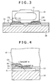
- connection terminal portions may be provided on the bottom face and side face, respectively, of the LED package, or as in the LED package mounting structure according to Comparative Example 1 shown in Fig. 3 , the connection terminal portions may be provided only on the bottom face of the LED package.
- the LED package and LED package mounting structure comprise the connection terminal portions for connecting with the circuit board on at least the bottom face of the LED package, and are mounted on the circuit board via the connection terminal portions in such a manner that the light-emitting surface is perpendicular to the mounting surface.
- the LED package mounting structure according to the embodiment of the present invention is characterized in that the shape of the solder is optimized by defining the relative position relation between the electrode on the bottom face of the LED package body and the component mounting pad on the circuit board. That is, in the LED package mounting structure according to the embodiment of the present invention, in a cross section of the mounting structure taken parallel to the LED light-emitting surface (a cross section in the direction of the LED light-emitting surface), the electrode on the bottom face of the LED package body is formed in a curved shape at an end portion of the electrode on the central side of the LED package, and when the curved portion is approximated to a curved line and the intersection of the tangent at the electrode end (P) and the circuit board is (Q), an end (R) of the component mounting pad on the central side of the LED package of the circuit board is located at point (Q), or is located closer to point (P) rather than point (Q).
- this metallized layer comprising W and other elements has poor solder wettability, and therefore a void 41 is likely to be generated on its exposed surface.
- a void 41 is likely to be generated on its exposed surface.
- Comparative Example 2 shown in Fig. 4 there is no gap or only a small gap between the LED package body 10 and the solder 30 in the vicinity of the burr 40 of the connection terminal portions 131, 132. Accordingly, the void 41 generated during reflow of the solder 30 remains without being removed, and the fatigue life of the solder 30 is reduced.
- the shape of the solder is optimized by defining the relative position relation between the electrode on the bottom face of the LED package body 10 and the component mounting pad on the circuit board 20 as in the present invention, the void 41 is easily removed, resulting in improved solder fatigue life.
- (R) is preferably located closer to the center of the package than the position (0.9 ⁇ L) from the side face side of the package.
- the effective path length until the occurrence of complete rupture of the solder is increased.
- the structure of the component mounting pad on the circuit board side may be the NSMD (Non Solder Mask Defined) structure, where the solder resist does not cover the end of the pad as shown in Fig. 5 , or may be the SMD (Solder Mask Defined) structure, where the solder resist covers the surface of the end of the pad as shown in Fig. 6 .
- the end of the pad is employed as point (R) in the NSMD structure
- the end of the opening of the solder resist is employed as point (R) in the SMD structure.
- the materials of the LED package, circuit board and solder used in the test are the same as those used in the simulation analysis of the first and second examples (refer to Table 1).
- the size of the LED package is 1 mm (length) ⁇ 3 mm (width) ⁇ 1.4 mm (height), and an anode and a cathode each having the size of 0.8 mm (length) ⁇ 0.9 mm (width) are disposed on the bottom face of the package at an interval of 1.2 mm.
- the LED package was mounted on the circuit board by soldering in the manner described above.
- the size of the circuit board pad was 0.9 mm (length) ⁇ 1.0 mm (width) both on the anode and cathode side, and the interval between the pads was 1.1 mm ( Embodiment).
- a sample with the size of the circuit board pad of 0.9 mm (length) ⁇ 1.1 mm (width) and an interval between the pads of 0.9 mm was also prepared (Comparative Example 2).
- the thickness of the solder after being mounted was 50 ⁇ m.
- the pad end (R) of the circuit board was located closer to the side face side of the package than point (Q), while in the sample of Comparative Example 2, the pad end (R) of the circuit board was located closer to the central side of the package than point (Q). Furthermore, in the sample of the third embodiment, the outline of the solder in a cross section was in the form a uniform curve. In contrast, in the sample of Comparative Example 2, as for the one-sided differential coefficient at the end (P) of the electrode of the package, a singular point where the left-sided differential coefficient and the right-sided differential coefficient do not match was generated.
- the samples were embedded in resin, and then cut with a diamond cutter to polish their cross sections.
- the crack propagation rate expresses the ratio of the crack length to the contact length between the electrode of the LED package and the solder in the actual cross section.
- Crack propagation rate (%) 500 cycles 1000 cycles 1250 cycles Third emobodiment 7.1 14.3 24.0 Comparative Example 2 18.5 67.2 (*) * Including samples which have caused complete fracture
- the embodiment of the present invention by defining the relative position relation between the end of the electrode of the central side of the LED package on the bottom face of the LED package body and the end of the component mounting pad on the circuit board to optimize the shape of the solder in a cross section of the LED package mounting structure taken parallel to the LED light-emitting surface (a cross section in the direction of the LED light-emitting surface), the generation of the singular point where stress is likely to be concentrated can be prevented, and further voids in the solder formed by burrs generated in the electrode portion of the package can be prevented. Therefore, even when there is a difference in the coefficients of linear expansion between the LED package and the circuit board, the fatigue life of solder which electrically connects the LED package and the circuit board can be improved, and continuity failure can be prevented.
- the present invention can be applied to liquid crystal displays comprising the LED package and LED package mounting structure described in the embodiment.
Landscapes
- Engineering & Computer Science (AREA)
- Manufacturing & Machinery (AREA)
- Microelectronics & Electronic Packaging (AREA)
- Led Device Packages (AREA)
- Wire Bonding (AREA)
Description
- This application relates to and claims priority from Japanese Patent Application No.
2010-080104, filed on March 31, 2010 - The present invention relates to an LED package, an LED package mounting structure comprising an LED package mounted on a circuit board such as a printed circuit board, and a liquid crystal display comprising an LED package mounting structure.
- In recent years, LEDs are increasingly used as light sources of backlight units for liquid crystal displays of televisions and monitors. This current corresponds to the demands for improved efficiencies of liquid crystal displays, and by using LED light sources, the power consumption and thickness of television sets can be reduced compared to conventional cold cathode fluorescent tubes. In particular, by realizing area control, which is controlling LEDs constituting the backlight unit by dividing them into a plurality of groups and controlling the luminance of the LEDs group by group depending on the content of the image, power consumption can be further lowered and high-resolution imaging is achieved.
- Backlight systems of liquid crystal displays which allow area control are roughly divided into direct lighting systems and slim block systems. In the direct lighting system, a number of LED light sources are dispersedly disposed within a plane in such a manner that their optical axes are perpendicular to a liquid crystal panel, and the light rays are mixed by a diffuser which is disposed at a point some distance from the light sources to homogenize luminance. Meanwhile, a slim block system is so constituted that a plurality of combinations of a plurality of LEDs and a series of light guide plates are arranged within a plane two-dimensionally, and the LEDs are disposed beside the light guide plates in such a manner that their optical axes are parallel to the liquid crystal panel. A light ray emitted from a light source is, when it is incident from the side face of a light guide plate, totally reflected within the light guide plate, propagated, scattered by reflecting dots or other elements formed on the bottom face of the light guide plate, and is taken out at the top face of the light guide plate. Since the slim block system does not require a space to obtain uniform luminance distribution within the plane, as opposed to the direct lighting system, it can be formed more thinly.
- When the slim block system is employed, in order to use a generic upward-lighting type surface mounted LED package (hereinafter referred to as a top-view type LED package) with which the optical axis is perpendicular to the mounting surface of the LED package, a relay board needs to be joined to a circuit board by soldering perpendicularly after LEDs are mounted on the relay board, or the relay board needs to be fixed perpendicularly to a chassis and then wired with a connector or other parts. This increases the number of parts and assembly steps and thus increases the costs.
- When the side-view type LED package is used, the LEDs are directly mounted on a circuit board such as a printed circuit board, and therefore the costs can be advantageously reduced.
-
US 2009/139755 A1 discloses a surface mounted structure with the features of the preamble of present claim 1. Another prior art example is described inUS 2010/025722 A1 . - Mounting the side-view type LED package of Japanese Patent Application Laid-Open Publication No.
H7-115227 - A possible solution for the problem stated above is increasing the amount of solder provided to increase the solder thickness in the joint portion, but increasing the solder thickness lowers the mounting accuracy of the LED package relative to the circuit board. That is, an increased positional shift of the LED package in the front-back and left-right directions, or inclination or rotation of the light-emitting surface of the LED package in the front-back direction lowers its optical coupling efficiency with the light guide plate. Another possible solution is to employ other connection means such as a thermosetting resin containing solder as a substitution for solder, but it is not practical since it leads to increased costs of components.
- In view of the problems mentioned above, an object of the present invention is to provide an LED package and an LED package mounting structure which can improve the fatigue life of solder which electrically connects an LED package and a circuit board even when there is a difference in the coefficients of linear expansion between the LED package and the circuit board, and prevent continuity failure at low costs.
- The above object can be achieved by the LED package mounting structure defined in claim 1. Disclosed is an example comprising an LED element mounted on a package body, the package body being mounted on a circuit board in such a manner that its light-emitting surface intersects the mounting surface, and the LED package comprising a first connection terminal portion for connecting with the circuit board on the side face of the package.
- Further disclosed is an LED package mounting structure comprising an LED package and a circuit board on which the LED package is mounted, the LED package and the circuit board being electrically connected by soldering, the LED package having a light-emitting surface in the direction of intersecting the mounting surface of the circuit board, comprising a first connection terminal portion on the side face of the package, and being joined with the circuit board by soldering via the connection terminal portion.
- Furthermore, disclosed is an LED package mounting structure comprising an LED package, and a connection terminal portion for connecting with a circuit board on the bottom face of the package, the LED package mounting structure being mounted on the circuit board in such a manner that a light-emitting surface of the LED package intersects the mounting surface via the connection terminal portion, in which in a cross section of the mounting structure in the direction of the LED light-emitting surface, an electrode on the bottom face of the LED package body is formed in a curved shape at an end portion of the electrode on the central side of the LED package, and when the curved portion is approximated to a curved line and the intersection of the tangent at the electrode end (P) and the circuit board is (Q), the end of the component mounting pad (R) on the central side of the LED package of the circuit board is located at point (Q) or located closer to point (P) than point (Q).
- Furthermore, disclosed is an LED package mounting structure comprising an LED package and a connection terminal portion for connecting with a circuit board on the bottom face of the package, the LED package mounting structure being mounted on the circuit board in such a manner that a light-emitting surface of the LED package intersects the mounting surface via the connection terminal portion, wherein in a cross section of the LED package mounting structure in the direction of the LED light-emitting surface, an electrode on the bottom face of the LED package body is formed in a curved shape at an end portion of the electrode on the central side of the LED package, and when the outline of the solder portion is approximated to a curved line, the inclination of the tangent of the outline of the solder is continuous at the end (P) of the electrode.
- According to the present invention, even when there is a difference in the coefficients of linear expansion between the LED package and the circuit board, the fatigue life of solder which electrically connects the LED package and the circuit board can be improved, and the LED package and LED package mounting structure which can prevent continuity failure can be provided at low costs.
- The present invention will become fully understood from the detailed description given hereinafter and the accompanying drawings, wherein:
-
Fig. 1 is a schematic front cross-sectional view of the LED package and LED package mounting structure according to a first example useful to understand the present invention; -
Fig. 2 is a schematic front cross-sectional view of the LED package and LED package mounting structure according to a second example useful to understand the present invention; -
Fig. 3 is a schematic front cross-sectional view of the LED package and LED package mounting structure according to Comparative Example 1 of the present invention; -
Fig. 4 is an enlarged cross-sectional view of an electrode portion on the bottom face of the package in the LED package and LED package mounting structure according to Comparative Example 2 of the present invention; -
Fig. 5 is an enlarged cross-sectional view of an electrode portion on the bottom face of the package in the LED package and LED package mounting structure according to an embodiment of the present invention (substrate pad: NSMD structure); and -
Fig. 6 is an enlarged cross-sectional view of an electrode portion on the bottom face of the package in the LED package and LED package mounting structure according to the embodiment of the present invention (substrate pad: SMD structure). - When a side-view type LED package is mounted on a circuit board by soldering as in Japanese Patent Application Laid-Open Publication No.
H7-115227 - An embodiment and two examples useful to understand the present invention in view of the problems mentioned above will be described below with reference to accompanying drawings.
-
Fig. 1 shows a schematic front cross-sectional view of an LED package and an LED package mounting structure according to the first example useful to understand the present invention. - The LED package mounting structure comprises a surface mount
type LED package 10 which is electrically connected to acircuit board 20 via solder. Herein, theLED package 10 has a case made of a ceramic sintered body produced by laminating a plurality of green sheets comprising alumina as a main component and calcining the same, and an LED element (not shown) is mounted inside the case. As the ceramic material, aluminium nitride, silicon carbide and beryllium oxide may be used, in addition to alumina. A resin package such as polyamide may be used in place of the ceramic package mentioned above. - The material used for the circuit board on which the LED package is mounted may be relatively inexpensive organic resin substrates such as glass epoxy board, as well as ceramic-based substrates having excellent reliability and metal-based substrates having excellent thermal conductivity, and is not particularly limited.
- The LED package is mounted in such a manner that its light-emitting surface 11 (parallel to the plane of the paper) is perpendicular to the mounting surface (perpendicular to the plane of the paper) of the circuit board (in an intersecting manner). The LED package has, in a state of being mounted, connection
terminal portions connection terminal portions anode electrode pad 121 and side facecathode electrode pad 122 can have any size as long as they can be installed on the side faces of the package. - The connection terminal portions are connected to
component mounting pads 21 on the circuit board viasolder 30. Herein, in the component mounting pad (or solder resist opening portion) on the side of thecircuit board 20 connected with theconnection terminal portions surface 11 of the package 10 (hereinafter referred to as size A) is desirably 0.5 to 2 times the pad size in the height direction of theconnection terminal portions - The area of the component mounting pad on the circuit board side connected with the connection terminal portions of the package (or the area of the solder resist openings) is preferably as large as possible within such a range that an appropriate solder fillet shape is formed. This is because a large pad area provides a large connection area of the solder, which results in an improvement of radiation characteristic and a reduction in heat stress caused by turning on/off the LED, and an increase in the effective path length until the solder completely fractures.
- A material used for the
solder 30 used to connect the LED package and the circuit board is preferably tin-silver binary eutectic solder having excellent thermal fatigue characteristics, tin-silver-copper ternary eutectic solder or tin-zinc-based solder. Specific examples include Sn-3.5Ag (melting point: about 221°C), Sn-3Ag-0.5Cu (melting point: about 217°C), Sn-9Zn (melting point: about 199°C), among others. It goes without saying that tin-lead eutectic alloy, which has been often used and has excellent joining property and fatigue life characteristics, is also usable. - A method for producing the LED package mounting structure will be now described. When the LED package is connected to the circuit board, the component mounting pad on the circuit board is preliminarily provided with solder by paste printing, dispenser application, metal plating or other means.
- The
LED package 10 is transferred with theconnection terminal portions circuit board 20 with theLED package 10 mounted thereon is conveyed on a belt into a reflow furnace. After the circuit board is heated inside the reflow furnace for a certain period of time at a temperature not lower than the melting point of the solder to once fuse the solder, the circuit board is drawn out from the reflow furnace by belt conveyance. The reflow furnace has some heating zones with different temperature settings. After the circuit board passes through the heating zone with the highest temperature setting, it is gradually cooled so that the solder is re-solidified. - The optimization of the fillet shape of the solder and the prevention of rise failure of the
LED package 10 according to the example described above can be realized by optimizing the amount of the solder provided and used, the size of the solder resist opening and the size of the pads of the circuit board, among other elements. - According to the mounting structure of the LED package of the example, the connection terminal portions are provided on the side face of the LED package, and a large area of the solder joint between the LED package and the circuit board on which the LED package is mounted can be provided. Therefore, even when there is a difference in the coefficients of linear expansion between the LED package and the circuit board, the fatigue life of solder which electrically connects the LED package and the circuit board can be improved, and continuity failure can be prevented.
-
Fig. 2 shows a schematic front cross-sectional view of an LED package and an LED package mounting structure according to the second example useful to understand the present invention. - The example is a partial modification of the first example above, where like portions having similar functions to those in the above-described example are designated by like numerals, and detailed description for like parts are omitted.
- The material of the LED package in the LED package mounting structure according to the second example and the material of the circuit board on which the LED package is mounted are the same as those in the LED package mounting structure of the first example. However, the LED package mounting structure according to the second example has a structural difference from that according to the first example. The LED package mounting structure according to the second example is characterized in that it has connection terminal portions not only on the side face of the LED package, but also on the bottom face.
- That is, the LED package in the LED package mounting structure according to the second example is mounted in such a manner that its light-emitting
surface 11 is perpendicular to (intersecting) the mounting surface of the circuit board, and has, in a state of being mounted, secondconnection terminal portions connection terminal portions Fig. 2 and 131 inFig. 3 , 122 inFig. 2 and 132 inFig. 3 ) may be continuous and connected without being separated on the surface of the package, or may be separate and independent on the surface of the package and electrically connected by the internal wiring of the package. - The method for producing the solder material used to connect the LED package and circuit board, and the LED package mounting structure is similar to that described in the first example.
- In order to confirm the effects of the LED package mounting structure according to the first and second examples, the results of simulation analysis will be described below. The fatigue life in the solder joint portion is represented by the sum of the lifetime until a minute crack initiates in the solder joint portion (crack initiation life) and the lifetime until the crack propagates and the solder joint portion fractures after the crack initiation life (crack propagation life). In order to determine the fatigue life of the solder joint portion, a crack propagation analysis for simulating a heat cycle test was conducted. An evaluation method which takes the cumulative damage of the solder into consideration was used for the analysis. This method automatically calculates the path and speed of crack propagation by evaluating the life of the solder in each position based on the damage accumulated at crack initiation and propagation. In the LED package mounting structure to be analyzed, an LED package having the size of 0.8 mm (length) × 3 mm (width) × 1.4 mm (height) is mounted on one side of the circuit board having the size of 0.96 mm (length) × 13.04 mm (width) × 0.4 mm (thickness). As the LED package, a model (First Example) in which a connecting terminal having the size of 0.92 mm (length) × 0.8 mm (width) is disposed on the side face and, as a comparison, a model (Comparative Example 1) in which a connecting terminal having the size of 0.8 mm (length) × 0.92 mm (width) is disposed on the bottom face were examined. The analysis was conducted on a 1/2 scale model of the mounting structure, considering symmetry.
- The materials and property values of each component used for the analytic models are shown in Table 1. The material of the LED package body was alumina, while the circuit board with the LED package mounted thereon was a printed circuit board using an epoxy resin. It was assumed that the solder was a temperature-dependent elasto-plastic solid, and that other materials were temperature-independent elastic bodies. The temperature cycle conditions were 125°C/-55°C. The fracture life of the solder based on the results of the analysis is shown in Table 2.
[Table 1] Component Material Linear expansion coefficient (ppm/°C) Young's modulus (GPa) Poisson's ratio LED package Alumina 6.3 380 0.3 Circuit board Epoxy resin 15 23 0.16 Solder Sn-3Ag-0.5Cu 23 41.3 (-50°C) 0.35 40.8 (-15°C) 38.2 (26°C) 35.5 (75°C) 33.8 (125°C) [Table 2] Position of electrode on package Electrode size (mm) Fracture life (cycle) First Example Side face 0.92 × 0.8 1211 Second Example Side face +
bottom face0.92 × 0.8 (side)
0.8 × 0.92 (bottom)> 1211 Comparative Example 1 Bottom face 0.8 × 0.92 (bottom) 1000 - As can be seen from Table 2, the samples of the first and second examples have larger numbers of cycles until the solder fractures than that of Comparative Example 1, indicating that effects in improving solder fatigue life were obtained.
- As mentioned above, by joining the package to the circuit board by soldering via the first and second connection terminal portions, a larger area of the solder joint between the package and the circuit board can be provided than in the first example. Therefore, even when there is a difference in the coefficients of linear expansion between the LED package and the circuit board, the fatigue life of the solder which electrically connects the LED package and the circuit board can be improved than that in the first example, and continuity failure can be prevented.
-
Fig. 5 shows an enlarged cross-sectional view of the electrode portion on the bottom face of the package in the LED package and LED package mounting structure according to the embodiment of the present invention. In the LED package mounting structure according to the embodiment, as in the LED package mounting structure according to the second example shown inFig. 2 , connection terminal portions may be provided on the bottom face and side face, respectively, of the LED package, or as in the LED package mounting structure according to Comparative Example 1 shown inFig. 3 , the connection terminal portions may be provided only on the bottom face of the LED package. In either case, the LED package and LED package mounting structure according to the embodiment of the present invention comprise the connection terminal portions for connecting with the circuit board on at least the bottom face of the LED package, and are mounted on the circuit board via the connection terminal portions in such a manner that the light-emitting surface is perpendicular to the mounting surface. - The LED package mounting structure according to the embodiment of the present invention is characterized in that the shape of the solder is optimized by defining the relative position relation between the electrode on the bottom face of the LED package body and the component mounting pad on the circuit board. That is, in the LED package mounting structure according to the embodiment of the present invention, in a cross section of the mounting structure taken parallel to the LED light-emitting surface (a cross section in the direction of the LED light-emitting surface), the electrode on the bottom face of the LED package body is formed in a curved shape at an end portion of the electrode on the central side of the LED package, and when the curved portion is approximated to a curved line and the intersection of the tangent at the electrode end (P) and the circuit board is (Q), an end (R) of the component mounting pad on the central side of the LED package of the circuit board is located at point (Q), or is located closer to point (P) rather than point (Q). By defining the relative position relation between the end of the electrode on the bottom face of the LED package body and the end of the component mounting pad on the circuit board as in the present invention, generation of singular points, where stress is likely to be concentrated, can be prevented in the solder portion, thereby improving solder fatigue life.
- Unlike the present invention, when the pad end (R) is located closer to the center of the package than point (Q) (in
Fig. 5 , right to point (Q)), as Comparative Example 2 shown inFig. 4 , in a cross section of the LED package mounting structure taken parallel to the LED light-emitting surface (a cross section in the direction of the LED light-emitting surface), when the outline of the solder portion is approximated to a curved line, as for the one-sided differential coefficient at the end (P) of the electrode of the package, a singular point where the left-sided differential coefficient and right-sided differential coefficient (equivalent to the inclination of tangent A and tangent B inFig. 4 ) do not match (that is, the inclinations of the tangents vary) is generated. Since stress is likely to be concentrated at the singular point, the fatigue life of the solder is reduced. In addition, when the end (R) of the pad is located closer to the central side of the package than point (Q), as Comparative Example 2 shown inFig. 4 , voids are likely to remain in the solder as a result. This is because of the following reason: in the electrode portion of the package, aburr 40 is generated during a dicing process for dividing the assembled board of the LED package into individual pieces, and the surface of the metallized layer comprising W or other elements with no metal plating film formed thereon is exposed. The surface of this metallized layer comprising W and other elements has poor solder wettability, and therefore a void 41 is likely to be generated on its exposed surface. In particular, in the case of Comparative Example 2 shown inFig. 4 , there is no gap or only a small gap between theLED package body 10 and thesolder 30 in the vicinity of theburr 40 of theconnection terminal portions solder 30 remains without being removed, and the fatigue life of thesolder 30 is reduced. - In other words, when the shape of the solder is optimized by defining the relative position relation between the electrode on the bottom face of the
LED package body 10 and the component mounting pad on thecircuit board 20 as in the present invention, the void 41 is easily removed, resulting in improved solder fatigue life. - When the end (R) of the pad is located closer to point (P) than point (Q) (in
Fig. 5 , left to point (Q)), assuming that the length of the electrode at the bottom of the package is L, (R) is preferably located closer to the center of the package than the position (0.9 × L) from the side face side of the package. In this case, since the joint area between the solder and the electrode of the package is increased than in the case where (R) is located closer to the side face of the package than the position (0.9 × L) from the side face side of the package, the effective path length until the occurrence of complete rupture of the solder is increased. - The structure of the component mounting pad on the circuit board side may be the NSMD (Non Solder Mask Defined) structure, where the solder resist does not cover the end of the pad as shown in
Fig. 5 , or may be the SMD (Solder Mask Defined) structure, where the solder resist covers the surface of the end of the pad as shown inFig. 6 . In this case, the end of the pad is employed as point (R) in the NSMD structure, while the end of the opening of the solder resist is employed as point (R) in the SMD structure. - The results of the solder fatigue life evaluation conducted in real device testing to confirm the effects of the LED package mounting structure according to the embodiment of the present invention will be described.
- The materials of the LED package, circuit board and solder used in the test are the same as those used in the simulation analysis of the first and second examples (refer to Table 1).
- The size of the LED package is 1 mm (length) × 3 mm (width) × 1.4 mm (height), and an anode and a cathode each having the size of 0.8 mm (length) × 0.9 mm (width) are disposed on the bottom face of the package at an interval of 1.2 mm.
- The LED package was mounted on the circuit board by soldering in the manner described above. The size of the circuit board pad was 0.9 mm (length) × 1.0 mm (width) both on the anode and cathode side, and the interval between the pads was 1.1 mm ( Embodiment). As a comparison, a sample with the size of the circuit board pad of 0.9 mm (length) × 1.1 mm (width) and an interval between the pads of 0.9 mm was also prepared (Comparative Example 2). The thickness of the solder after being mounted was 50 µm. In the sample of the embodiment, the pad end (R) of the circuit board was located closer to the side face side of the package than point (Q), while in the sample of Comparative Example 2, the pad end (R) of the circuit board was located closer to the central side of the package than point (Q). Furthermore, in the sample of the third embodiment, the outline of the solder in a cross section was in the form a uniform curve. In contrast, in the sample of Comparative Example 2, as for the one-sided differential coefficient at the end (P) of the electrode of the package, a singular point where the left-sided differential coefficient and the right-sided differential coefficient do not match was generated. That is, in the sample of the embodiment, when the outline of the solder in a cross section is approximated to a curved line, the inclination of the tangent at the end (P) of the electrode of the package is continuous (changing smoothly). In contrast, in the sample of Comparative Example 2, when the outline of the solder in a cross section is approximated to a curved line, a singular point where the inclination of the tangent at the end (P) of the electrode of the package is discontinuous (abruptly changing) is formed.
- The test samples were fed into a temperature cycling test chamber (125°C/-55°C) at ΔT=180°C, and were drawn out after a certain number of cycles. The samples were embedded in resin, and then cut with a diamond cutter to polish their cross sections. The crack propagation rate (average, n=4) of the solder determined by photographing the ground surfaces with a scanning electron microscope (SEM) are shown in Table 3. The crack propagation rate expresses the ratio of the crack length to the contact length between the electrode of the LED package and the solder in the actual cross section.
[Table 3] Crack propagation rate (%) 500 cycles 1000 cycles 1250 cycles Third emobodiment 7.1 14.3 24.0 Comparative Example 2 18.5 67.2 (*) * Including samples which have caused complete fracture - As can be seen from Table 3, the sample of the embodiment had a slower rate of crack propagation than that of Comparative Example 2, indicating that improvement in solder fatigue life has been achieved by the LED package mounting structure according to the present invention.
- As mentioned above, according to the embodiment of the present invention, by defining the relative position relation between the end of the electrode of the central side of the LED package on the bottom face of the LED package body and the end of the component mounting pad on the circuit board to optimize the shape of the solder in a cross section of the LED package mounting structure taken parallel to the LED light-emitting surface (a cross section in the direction of the LED light-emitting surface), the generation of the singular point where stress is likely to be concentrated can be prevented, and further voids in the solder formed by burrs generated in the electrode portion of the package can be prevented. Therefore, even when there is a difference in the coefficients of linear expansion between the LED package and the circuit board, the fatigue life of solder which electrically connects the LED package and the circuit board can be improved, and continuity failure can be prevented.
- Although the LED package and the LED package mounting structure according to the present invention have been described in the embodiment, the present invention can be applied to liquid crystal displays comprising the LED package and LED package mounting structure described in the embodiment.
- The embodiment described above is only a specific embodiment for carrying out the present invention, and the scope of the present invention must not be construed to be limited by them. The present invention can be carried out in various forms without departing from the scope of the invention as defined in the appended claims.
Claims (2)
- An LED package mounting structure comprising:an LED package (10); anda connection terminal portion (131, 132) on the bottom face of the package (10) for connecting with a component mounting pad (21) of a circuit board (20) via a solder (30),the LED package mounting structure being mounted on the circuit board (20) in such a manner that a light-emitting surface (11) of the LED package (10) intersects a mounting surface via the connection terminal portion (131, 132),in a cross section of the mounting structure taken parallel to the LED light-emitting surface (11), an electrode on the bottom face of an LED package body being formed in a curved shape at an end portion of the electrode on the central side of the LED package (10),characterised in that
when the curved shape is approximated to a curved line and the intersection of a tangent to the curved line at an electrode end point (P) and the circuit board (20) is at an intersection point (Q), an end (R) of the component mounting pad (21) on the central side of the LED package (10) of the circuit board (20) is located at the intersection point (Q), or is located closer to the end point (P) than the intersection point (Q), and
the intersection point (Q) is located closer to the central side of the LED package (10) than the end (R) of the component mounting pad (21). - A liquid crystal display comprising the LED package mounting structure according to claim 1.
Applications Claiming Priority (1)
| Application Number | Priority Date | Filing Date | Title |
|---|---|---|---|
| JP2010080104A JP2011216506A (en) | 2010-03-31 | 2010-03-31 | Led package and led package mounting structure |
Publications (2)
| Publication Number | Publication Date |
|---|---|
| EP2372793A1 EP2372793A1 (en) | 2011-10-05 |
| EP2372793B1 true EP2372793B1 (en) | 2012-12-12 |
Family
ID=43799735
Family Applications (1)
| Application Number | Title | Priority Date | Filing Date |
|---|---|---|---|
| EP10014139A Not-in-force EP2372793B1 (en) | 2010-03-31 | 2010-10-29 | LED package mounting structure |
Country Status (4)
| Country | Link |
|---|---|
| US (1) | US8716741B2 (en) |
| EP (1) | EP2372793B1 (en) |
| JP (1) | JP2011216506A (en) |
| CN (1) | CN102208515B (en) |
Families Citing this family (17)
| Publication number | Priority date | Publication date | Assignee | Title |
|---|---|---|---|---|
| DE102010029368B4 (en) * | 2010-05-27 | 2026-02-19 | OSRAM Opto Semiconductors Gesellschaft mit beschränkter Haftung | Electronic arrangement |
| TW201230910A (en) * | 2011-01-11 | 2012-07-16 | Hon Hai Prec Ind Co Ltd | The method of manufacturing the LED lightbar and the equipment thereof |
| TW201251140A (en) * | 2011-01-31 | 2012-12-16 | Cree Inc | High brightness light emitting diode (LED) packages, systems and methods with improved resin filling and high adhesion |
| WO2012109225A1 (en) | 2011-02-07 | 2012-08-16 | Cree, Inc. | Components and methods for light emitting diode (led) lighting |
| TW201316368A (en) * | 2011-10-14 | 2013-04-16 | Primax Electronics Ltd | Illuminating keyboard |
| JP6024200B2 (en) * | 2012-05-18 | 2016-11-09 | 富士電機機器制御株式会社 | Electronic component mounting method on surface mount board |
| JP2014110370A (en) * | 2012-12-04 | 2014-06-12 | Seiko Epson Corp | Base substrate, mounting structure, module, electronic equipment, and mobile object |
| JP6036303B2 (en) * | 2013-01-07 | 2016-11-30 | セイコーエプソン株式会社 | Package, optical module, and electronic device |
| CN103594568A (en) * | 2013-10-24 | 2014-02-19 | 天津三安光电有限公司 | Semiconductor device and manufacturing method thereof |
| EP3278920B1 (en) * | 2014-04-02 | 2020-03-04 | Senju Metal Industry Co., Ltd. | Use of a solder alloy for bonding in a module |
| TWI606207B (en) * | 2014-10-14 | 2017-11-21 | 鴻海精密工業股份有限公司 | Light source module |
| JP6504019B2 (en) * | 2015-10-27 | 2019-04-24 | 豊田合成株式会社 | Light emitting device |
| DE102017115780A1 (en) * | 2017-07-13 | 2019-01-17 | Tdk Electronics Ag | Light-emitting diode component, light-emitting diode arrangement and method for producing a light-emitting diode component |
| CN109873072B (en) * | 2017-12-01 | 2021-09-21 | 光宝科技新加坡私人有限公司 | Light emitting device, light emitting diode packaging structure and manufacturing method thereof |
| TWI682695B (en) * | 2018-07-05 | 2020-01-11 | 同泰電子科技股份有限公司 | Circuit board structure with conection terminal formed by solder mask defined process |
| US11521917B2 (en) * | 2019-05-23 | 2022-12-06 | Rohm Co., Ltd. | Semiconductor device |
| KR102812715B1 (en) * | 2021-12-30 | 2025-05-27 | 주식회사 아모텍 | Multi-layer ceramic capacitor and manufacturing method thereof |
Family Cites Families (23)
| Publication number | Priority date | Publication date | Assignee | Title |
|---|---|---|---|---|
| US5315070A (en) * | 1991-12-02 | 1994-05-24 | Siemens Aktiengesellschaft | Printed wiring board to which solder has been applied |
| JPH07115227B2 (en) | 1992-03-04 | 1995-12-13 | 株式会社栗本鐵工所 | Scotch yoke press |
| JP2802411B2 (en) * | 1992-05-26 | 1998-09-24 | シャープ株式会社 | Optical device |
| JP3152834B2 (en) * | 1993-06-24 | 2001-04-03 | 株式会社東芝 | Electronic circuit device |
| JPH07115227A (en) | 1993-10-15 | 1995-05-02 | Rohm Co Ltd | Light emitting device and light emitting unit using the same |
| JP3447139B2 (en) | 1995-03-06 | 2003-09-16 | 株式会社シチズン電子 | Chip type light emitting diode |
| JP3158018B2 (en) * | 1995-07-17 | 2001-04-23 | シャープ株式会社 | Horizontal light emitting LED and method for manufacturing the same |
| JP3576727B2 (en) * | 1996-12-10 | 2004-10-13 | 株式会社デンソー | Surface mount type package |
| JP4440381B2 (en) * | 1999-08-31 | 2010-03-24 | ローム株式会社 | Infrared transceiver module |
| US6787884B2 (en) * | 2002-05-30 | 2004-09-07 | Matsushita Electric Industrial Co., Ltd. | Circuit component, circuit component package, circuit component built-in module, circuit component package production and circuit component built-in module production |
| TWI228303B (en) * | 2003-10-29 | 2005-02-21 | Advanced Semiconductor Eng | Semiconductor package, method for manufacturing the same and lead frame for use in the same |
| JP4792726B2 (en) | 2003-10-30 | 2011-10-12 | 日亜化学工業株式会社 | Manufacturing method of support for semiconductor element |
| US7245024B2 (en) * | 2005-01-21 | 2007-07-17 | Delphi Technologies, Inc. | Electronic assembly with reduced leakage current |
| TW200711190A (en) | 2005-08-17 | 2007-03-16 | Matsushita Electric Industrial Co Ltd | Surface mounted semiconductor device and method for manufacturing same |
| JP2008147605A (en) | 2006-11-14 | 2008-06-26 | Harison Toshiba Lighting Corp | LIGHT EMITTING DEVICE, ITS MANUFACTURING METHOD, AND MOUNTING BOARD |
| US20100025722A1 (en) * | 2006-11-14 | 2010-02-04 | Harison Toshiba Lighting Corp. | Light emitting device, its manufacturing method and its mounted substrate |
| US7893545B2 (en) * | 2007-07-18 | 2011-02-22 | Infineon Technologies Ag | Semiconductor device |
| US7737546B2 (en) * | 2007-09-05 | 2010-06-15 | Avago Technologies Ecbu Ip (Singapore) Pte. Ltd. | Surface mountable semiconductor package with solder bonding features |
| US7830022B2 (en) * | 2007-10-22 | 2010-11-09 | Infineon Technologies Ag | Semiconductor package |
| KR101535064B1 (en) * | 2008-01-17 | 2015-07-09 | 삼성디스플레이 주식회사 | Light source module for display device and display device including same |
| KR100957411B1 (en) * | 2008-02-05 | 2010-05-11 | 엘지이노텍 주식회사 | Light emitting device |
| JP5211801B2 (en) * | 2008-03-28 | 2013-06-12 | Tdk株式会社 | Electronic components |
| JP5211983B2 (en) | 2008-09-24 | 2013-06-12 | 住友電装株式会社 | connector |
-
2010
- 2010-03-31 JP JP2010080104A patent/JP2011216506A/en active Pending
- 2010-10-20 US US12/908,507 patent/US8716741B2/en not_active Expired - Fee Related
- 2010-10-29 EP EP10014139A patent/EP2372793B1/en not_active Not-in-force
- 2010-10-29 CN CN201010530500.8A patent/CN102208515B/en not_active Expired - Fee Related
Also Published As
| Publication number | Publication date |
|---|---|
| JP2011216506A (en) | 2011-10-27 |
| US8716741B2 (en) | 2014-05-06 |
| US20110242450A1 (en) | 2011-10-06 |
| CN102208515A (en) | 2011-10-05 |
| CN102208515B (en) | 2014-01-08 |
| EP2372793A1 (en) | 2011-10-05 |
Similar Documents
| Publication | Publication Date | Title |
|---|---|---|
| US8716741B2 (en) | LED package and LED package mounting structure | |
| CN102473828B (en) | Mounting substrate for semiconductor light emitting element, backlight chassis, and display device | |
| US8198540B2 (en) | Power element mounting substrate, method of manufacturing the same, power element mounting unit, method of manufacturing the same, and power module | |
| KR101194429B1 (en) | Semiconductor device and method for producing the same | |
| EP2259308B1 (en) | Substrate for power module with heat sink and method for producing the same, power module with heat sink, and substrate for power module | |
| KR100482940B1 (en) | High density column grid array connections and method thereof | |
| CN103000559B (en) | The positioning fixture of semiconductor chip and the manufacture method of semiconductor device | |
| US20050110161A1 (en) | Method for mounting semiconductor chip and semiconductor chip-mounted board | |
| US20110024785A1 (en) | Light Emitting Diode Device | |
| CN1551340A (en) | Semiconductor device and manufacturing method thereof | |
| KR20140142256A (en) | Power module substrate with heat sink, power module substrate with cooler, and power module | |
| US10843284B2 (en) | Method for void reduction in solder joints | |
| US20060261455A1 (en) | LED package structure and method making of the same | |
| CN1937887A (en) | Structure and method for reducing warp of substrate | |
| US20200146157A1 (en) | Method of Enhancing Fatigue Life of Grid Arrays | |
| KR20080033164A (en) | Linear light source device, surface light emitting device and liquid crystal display device | |
| JP2011134920A (en) | Led package mounting structure and manufacturing method thereof | |
| JP2009038184A (en) | Semiconductor light emitting device, light source device, and planar light emitting device | |
| JP5056327B2 (en) | Light emitting device | |
| JP2005039122A (en) | Light emitting device | |
| JP4560645B2 (en) | Heat sink for mounting a plurality of semiconductor substrates and semiconductor substrate assembly using the same | |
| JP5227677B2 (en) | LED mounting structure, LED light source, and backlight device including the same | |
| JP2011101054A (en) | Substrate for mounting semiconductor light emitting element, backlight chassis, display device, and television receiver | |
| JP4910789B2 (en) | Power element mounting substrate, power element mounting substrate manufacturing method, and power module | |
| JP2013098213A (en) | Method for manufacturing dual-sided mounting substrate |
Legal Events
| Date | Code | Title | Description |
|---|---|---|---|
| PUAI | Public reference made under article 153(3) epc to a published international application that has entered the european phase |
Free format text: ORIGINAL CODE: 0009012 |
|
| 17P | Request for examination filed |
Effective date: 20110225 |
|
| AK | Designated contracting states |
Kind code of ref document: A1 Designated state(s): AL AT BE BG CH CY CZ DE DK EE ES FI FR GB GR HR HU IE IS IT LI LT LU LV MC MK MT NL NO PL PT RO RS SE SI SK SM TR |
|
| AX | Request for extension of the european patent |
Extension state: BA ME |
|
| GRAP | Despatch of communication of intention to grant a patent |
Free format text: ORIGINAL CODE: EPIDOSNIGR1 |
|
| RIC1 | Information provided on ipc code assigned before grant |
Ipc: H01L 33/48 20100101AFI20120508BHEP Ipc: H05K 3/34 20060101ALI20120508BHEP |
|
| GRAS | Grant fee paid |
Free format text: ORIGINAL CODE: EPIDOSNIGR3 |
|
| GRAA | (expected) grant |
Free format text: ORIGINAL CODE: 0009210 |
|
| AK | Designated contracting states |
Kind code of ref document: B1 Designated state(s): AL AT BE BG CH CY CZ DE DK EE ES FI FR GB GR HR HU IE IS IT LI LT LU LV MC MK MT NL NO PL PT RO RS SE SI SK SM TR |
|
| REG | Reference to a national code |
Ref country code: GB Ref legal event code: FG4D |
|
| REG | Reference to a national code |
Ref country code: CH Ref legal event code: EP |
|
| REG | Reference to a national code |
Ref country code: AT Ref legal event code: REF Ref document number: 588701 Country of ref document: AT Kind code of ref document: T Effective date: 20121215 |
|
| REG | Reference to a national code |
Ref country code: IE Ref legal event code: FG4D |
|
| REG | Reference to a national code |
Ref country code: DE Ref legal event code: R096 Ref document number: 602010004026 Country of ref document: DE Effective date: 20130207 |
|
| PG25 | Lapsed in a contracting state [announced via postgrant information from national office to epo] |
Ref country code: NO Free format text: LAPSE BECAUSE OF FAILURE TO SUBMIT A TRANSLATION OF THE DESCRIPTION OR TO PAY THE FEE WITHIN THE PRESCRIBED TIME-LIMIT Effective date: 20130312 Ref country code: LT Free format text: LAPSE BECAUSE OF FAILURE TO SUBMIT A TRANSLATION OF THE DESCRIPTION OR TO PAY THE FEE WITHIN THE PRESCRIBED TIME-LIMIT Effective date: 20121212 Ref country code: ES Free format text: LAPSE BECAUSE OF FAILURE TO SUBMIT A TRANSLATION OF THE DESCRIPTION OR TO PAY THE FEE WITHIN THE PRESCRIBED TIME-LIMIT Effective date: 20130323 Ref country code: SE Free format text: LAPSE BECAUSE OF FAILURE TO SUBMIT A TRANSLATION OF THE DESCRIPTION OR TO PAY THE FEE WITHIN THE PRESCRIBED TIME-LIMIT Effective date: 20121212 Ref country code: FI Free format text: LAPSE BECAUSE OF FAILURE TO SUBMIT A TRANSLATION OF THE DESCRIPTION OR TO PAY THE FEE WITHIN THE PRESCRIBED TIME-LIMIT Effective date: 20121212 |
|
| REG | Reference to a national code |
Ref country code: NL Ref legal event code: VDEP Effective date: 20121212 |
|
| REG | Reference to a national code |
Ref country code: AT Ref legal event code: MK05 Ref document number: 588701 Country of ref document: AT Kind code of ref document: T Effective date: 20121212 |
|
| REG | Reference to a national code |
Ref country code: LT Ref legal event code: MG4D |
|
| PG25 | Lapsed in a contracting state [announced via postgrant information from national office to epo] |
Ref country code: LV Free format text: LAPSE BECAUSE OF FAILURE TO SUBMIT A TRANSLATION OF THE DESCRIPTION OR TO PAY THE FEE WITHIN THE PRESCRIBED TIME-LIMIT Effective date: 20121212 Ref country code: SI Free format text: LAPSE BECAUSE OF FAILURE TO SUBMIT A TRANSLATION OF THE DESCRIPTION OR TO PAY THE FEE WITHIN THE PRESCRIBED TIME-LIMIT Effective date: 20121212 Ref country code: GR Free format text: LAPSE BECAUSE OF FAILURE TO SUBMIT A TRANSLATION OF THE DESCRIPTION OR TO PAY THE FEE WITHIN THE PRESCRIBED TIME-LIMIT Effective date: 20130313 |
|
| PG25 | Lapsed in a contracting state [announced via postgrant information from national office to epo] |
Ref country code: BG Free format text: LAPSE BECAUSE OF FAILURE TO SUBMIT A TRANSLATION OF THE DESCRIPTION OR TO PAY THE FEE WITHIN THE PRESCRIBED TIME-LIMIT Effective date: 20130312 Ref country code: RS Free format text: LAPSE BECAUSE OF FAILURE TO SUBMIT A TRANSLATION OF THE DESCRIPTION OR TO PAY THE FEE WITHIN THE PRESCRIBED TIME-LIMIT Effective date: 20121212 Ref country code: SK Free format text: LAPSE BECAUSE OF FAILURE TO SUBMIT A TRANSLATION OF THE DESCRIPTION OR TO PAY THE FEE WITHIN THE PRESCRIBED TIME-LIMIT Effective date: 20121212 Ref country code: AT Free format text: LAPSE BECAUSE OF FAILURE TO SUBMIT A TRANSLATION OF THE DESCRIPTION OR TO PAY THE FEE WITHIN THE PRESCRIBED TIME-LIMIT Effective date: 20121212 Ref country code: CZ Free format text: LAPSE BECAUSE OF FAILURE TO SUBMIT A TRANSLATION OF THE DESCRIPTION OR TO PAY THE FEE WITHIN THE PRESCRIBED TIME-LIMIT Effective date: 20121212 Ref country code: IS Free format text: LAPSE BECAUSE OF FAILURE TO SUBMIT A TRANSLATION OF THE DESCRIPTION OR TO PAY THE FEE WITHIN THE PRESCRIBED TIME-LIMIT Effective date: 20130412 Ref country code: EE Free format text: LAPSE BECAUSE OF FAILURE TO SUBMIT A TRANSLATION OF THE DESCRIPTION OR TO PAY THE FEE WITHIN THE PRESCRIBED TIME-LIMIT Effective date: 20121212 Ref country code: BE Free format text: LAPSE BECAUSE OF FAILURE TO SUBMIT A TRANSLATION OF THE DESCRIPTION OR TO PAY THE FEE WITHIN THE PRESCRIBED TIME-LIMIT Effective date: 20121212 |
|
| PG25 | Lapsed in a contracting state [announced via postgrant information from national office to epo] |
Ref country code: RO Free format text: LAPSE BECAUSE OF FAILURE TO SUBMIT A TRANSLATION OF THE DESCRIPTION OR TO PAY THE FEE WITHIN THE PRESCRIBED TIME-LIMIT Effective date: 20121212 Ref country code: PL Free format text: LAPSE BECAUSE OF FAILURE TO SUBMIT A TRANSLATION OF THE DESCRIPTION OR TO PAY THE FEE WITHIN THE PRESCRIBED TIME-LIMIT Effective date: 20121212 Ref country code: PT Free format text: LAPSE BECAUSE OF FAILURE TO SUBMIT A TRANSLATION OF THE DESCRIPTION OR TO PAY THE FEE WITHIN THE PRESCRIBED TIME-LIMIT Effective date: 20130412 Ref country code: NL Free format text: LAPSE BECAUSE OF FAILURE TO SUBMIT A TRANSLATION OF THE DESCRIPTION OR TO PAY THE FEE WITHIN THE PRESCRIBED TIME-LIMIT Effective date: 20121212 |
|
| PLBE | No opposition filed within time limit |
Free format text: ORIGINAL CODE: 0009261 |
|
| STAA | Information on the status of an ep patent application or granted ep patent |
Free format text: STATUS: NO OPPOSITION FILED WITHIN TIME LIMIT |
|
| PG25 | Lapsed in a contracting state [announced via postgrant information from national office to epo] |
Ref country code: DK Free format text: LAPSE BECAUSE OF FAILURE TO SUBMIT A TRANSLATION OF THE DESCRIPTION OR TO PAY THE FEE WITHIN THE PRESCRIBED TIME-LIMIT Effective date: 20121212 |
|
| 26N | No opposition filed |
Effective date: 20130913 |
|
| PG25 | Lapsed in a contracting state [announced via postgrant information from national office to epo] |
Ref country code: HR Free format text: LAPSE BECAUSE OF FAILURE TO SUBMIT A TRANSLATION OF THE DESCRIPTION OR TO PAY THE FEE WITHIN THE PRESCRIBED TIME-LIMIT Effective date: 20121212 Ref country code: CY Free format text: LAPSE BECAUSE OF FAILURE TO SUBMIT A TRANSLATION OF THE DESCRIPTION OR TO PAY THE FEE WITHIN THE PRESCRIBED TIME-LIMIT Effective date: 20121212 |
|
| PG25 | Lapsed in a contracting state [announced via postgrant information from national office to epo] |
Ref country code: IT Free format text: LAPSE BECAUSE OF FAILURE TO SUBMIT A TRANSLATION OF THE DESCRIPTION OR TO PAY THE FEE WITHIN THE PRESCRIBED TIME-LIMIT Effective date: 20121212 |
|
| REG | Reference to a national code |
Ref country code: DE Ref legal event code: R097 Ref document number: 602010004026 Country of ref document: DE Effective date: 20130913 |
|
| PG25 | Lapsed in a contracting state [announced via postgrant information from national office to epo] |
Ref country code: MC Free format text: LAPSE BECAUSE OF FAILURE TO SUBMIT A TRANSLATION OF THE DESCRIPTION OR TO PAY THE FEE WITHIN THE PRESCRIBED TIME-LIMIT Effective date: 20121212 |
|
| REG | Reference to a national code |
Ref country code: IE Ref legal event code: MM4A |
|
| PG25 | Lapsed in a contracting state [announced via postgrant information from national office to epo] |
Ref country code: IE Free format text: LAPSE BECAUSE OF NON-PAYMENT OF DUE FEES Effective date: 20131029 |
|
| REG | Reference to a national code |
Ref country code: DE Ref legal event code: R082 Ref document number: 602010004026 Country of ref document: DE Representative=s name: PATENTANWAELTE STREHL, SCHUEBEL-HOPF & PARTNER, DE |
|
| REG | Reference to a national code |
Ref country code: GB Ref legal event code: 732E Free format text: REGISTERED BETWEEN 20150312 AND 20150318 |
|
| REG | Reference to a national code |
Ref country code: DE Ref legal event code: R081 Ref document number: 602010004026 Country of ref document: DE Owner name: HITACHI MAXELL, LTD., IBARAKI-SHI, JP Free format text: FORMER OWNER: HITACHI CONSUMER ELECTRONICS CO., LTD., TOKIO/TOKYO, JP Effective date: 20150317 Ref country code: DE Ref legal event code: R082 Ref document number: 602010004026 Country of ref document: DE Representative=s name: PATENTANWAELTE STREHL, SCHUEBEL-HOPF & PARTNER, DE Effective date: 20150317 Ref country code: DE Ref legal event code: R082 Ref document number: 602010004026 Country of ref document: DE Representative=s name: STREHL SCHUEBEL-HOPF & PARTNER MBB PATENTANWAE, DE Effective date: 20150317 |
|
| PG25 | Lapsed in a contracting state [announced via postgrant information from national office to epo] |
Ref country code: SM Free format text: LAPSE BECAUSE OF FAILURE TO SUBMIT A TRANSLATION OF THE DESCRIPTION OR TO PAY THE FEE WITHIN THE PRESCRIBED TIME-LIMIT Effective date: 20121212 |
|
| REG | Reference to a national code |
Ref country code: CH Ref legal event code: PL |
|
| REG | Reference to a national code |
Ref country code: FR Ref legal event code: TP Owner name: HITACHI MAXELL LTD., JP Effective date: 20150504 |
|
| PG25 | Lapsed in a contracting state [announced via postgrant information from national office to epo] |
Ref country code: TR Free format text: LAPSE BECAUSE OF FAILURE TO SUBMIT A TRANSLATION OF THE DESCRIPTION OR TO PAY THE FEE WITHIN THE PRESCRIBED TIME-LIMIT Effective date: 20121212 |
|
| PG25 | Lapsed in a contracting state [announced via postgrant information from national office to epo] |
Ref country code: LU Free format text: LAPSE BECAUSE OF NON-PAYMENT OF DUE FEES Effective date: 20131029 Ref country code: CH Free format text: LAPSE BECAUSE OF NON-PAYMENT OF DUE FEES Effective date: 20141031 Ref country code: MK Free format text: LAPSE BECAUSE OF FAILURE TO SUBMIT A TRANSLATION OF THE DESCRIPTION OR TO PAY THE FEE WITHIN THE PRESCRIBED TIME-LIMIT Effective date: 20121212 Ref country code: HU Free format text: LAPSE BECAUSE OF FAILURE TO SUBMIT A TRANSLATION OF THE DESCRIPTION OR TO PAY THE FEE WITHIN THE PRESCRIBED TIME-LIMIT; INVALID AB INITIO Effective date: 20101029 Ref country code: LI Free format text: LAPSE BECAUSE OF NON-PAYMENT OF DUE FEES Effective date: 20141031 |
|
| PG25 | Lapsed in a contracting state [announced via postgrant information from national office to epo] |
Ref country code: MT Free format text: LAPSE BECAUSE OF FAILURE TO SUBMIT A TRANSLATION OF THE DESCRIPTION OR TO PAY THE FEE WITHIN THE PRESCRIBED TIME-LIMIT Effective date: 20121212 |
|
| REG | Reference to a national code |
Ref country code: FR Ref legal event code: PLFP Year of fee payment: 7 |
|
| PGFP | Annual fee paid to national office [announced via postgrant information from national office to epo] |
Ref country code: FR Payment date: 20160919 Year of fee payment: 7 |
|
| PGFP | Annual fee paid to national office [announced via postgrant information from national office to epo] |
Ref country code: GB Payment date: 20161026 Year of fee payment: 7 Ref country code: DE Payment date: 20161025 Year of fee payment: 7 |
|
| REG | Reference to a national code |
Ref country code: DE Ref legal event code: R119 Ref document number: 602010004026 Country of ref document: DE |
|
| GBPC | Gb: european patent ceased through non-payment of renewal fee |
Effective date: 20171029 |
|
| REG | Reference to a national code |
Ref country code: FR Ref legal event code: ST Effective date: 20180629 |
|
| PG25 | Lapsed in a contracting state [announced via postgrant information from national office to epo] |
Ref country code: GB Free format text: LAPSE BECAUSE OF NON-PAYMENT OF DUE FEES Effective date: 20171029 Ref country code: DE Free format text: LAPSE BECAUSE OF NON-PAYMENT OF DUE FEES Effective date: 20180501 |
|
| PG25 | Lapsed in a contracting state [announced via postgrant information from national office to epo] |
Ref country code: FR Free format text: LAPSE BECAUSE OF NON-PAYMENT OF DUE FEES Effective date: 20171031 |
|
| PG25 | Lapsed in a contracting state [announced via postgrant information from national office to epo] |
Ref country code: AL Free format text: LAPSE BECAUSE OF FAILURE TO SUBMIT A TRANSLATION OF THE DESCRIPTION OR TO PAY THE FEE WITHIN THE PRESCRIBED TIME-LIMIT Effective date: 20121212 |