EP2372587B1 - Vorrichtung und Verfahren zur Simulierung eines rekonfigurierbaren Prozessors - Google Patents
Vorrichtung und Verfahren zur Simulierung eines rekonfigurierbaren Prozessors Download PDFInfo
- Publication number
- EP2372587B1 EP2372587B1 EP11154723.8A EP11154723A EP2372587B1 EP 2372587 B1 EP2372587 B1 EP 2372587B1 EP 11154723 A EP11154723 A EP 11154723A EP 2372587 B1 EP2372587 B1 EP 2372587B1
- Authority
- EP
- European Patent Office
- Prior art keywords
- processor
- routing
- operand
- simulation
- functional unit
- Prior art date
- Legal status (The legal status is an assumption and is not a legal conclusion. Google has not performed a legal analysis and makes no representation as to the accuracy of the status listed.)
- Active
Links
Images


Classifications
-
- G—PHYSICS
- G06—COMPUTING OR CALCULATING; COUNTING
- G06F—ELECTRIC DIGITAL DATA PROCESSING
- G06F30/00—Computer-aided design [CAD]
- G06F30/30—Circuit design
- G06F30/34—Circuit design for reconfigurable circuits, e.g. field programmable gate arrays [FPGA] or programmable logic devices [PLD]
- G06F30/347—Physical level, e.g. placement or routing
-
- G—PHYSICS
- G06—COMPUTING OR CALCULATING; COUNTING
- G06F—ELECTRIC DIGITAL DATA PROCESSING
- G06F9/00—Arrangements for program control, e.g. control units
- G06F9/06—Arrangements for program control, e.g. control units using stored programs, i.e. using an internal store of processing equipment to receive or retain programs
- G06F9/44—Arrangements for executing specific programs
- G06F9/455—Emulation; Interpretation; Software simulation, e.g. virtualisation or emulation of application or operating system execution engines
- G06F9/45504—Abstract machines for programme code execution, e.g. Java virtual machine [JVM], interpreters, emulators
-
- G—PHYSICS
- G06—COMPUTING OR CALCULATING; COUNTING
- G06F—ELECTRIC DIGITAL DATA PROCESSING
- G06F30/00—Computer-aided design [CAD]
- G06F30/30—Circuit design
- G06F30/32—Circuit design at the digital level
- G06F30/33—Design verification, e.g. functional simulation or model checking
-
- G—PHYSICS
- G06—COMPUTING OR CALCULATING; COUNTING
- G06F—ELECTRIC DIGITAL DATA PROCESSING
- G06F30/00—Computer-aided design [CAD]
- G06F30/30—Circuit design
- G06F30/32—Circuit design at the digital level
- G06F30/33—Design verification, e.g. functional simulation or model checking
- G06F30/3308—Design verification, e.g. functional simulation or model checking using simulation
-
- G—PHYSICS
- G06—COMPUTING OR CALCULATING; COUNTING
- G06F—ELECTRIC DIGITAL DATA PROCESSING
- G06F30/00—Computer-aided design [CAD]
- G06F30/30—Circuit design
- G06F30/34—Circuit design for reconfigurable circuits, e.g. field programmable gate arrays [FPGA] or programmable logic devices [PLD]
-
- G—PHYSICS
- G06—COMPUTING OR CALCULATING; COUNTING
- G06F—ELECTRIC DIGITAL DATA PROCESSING
- G06F30/00—Computer-aided design [CAD]
- G06F30/30—Circuit design
- G06F30/39—Circuit design at the physical level
- G06F30/394—Routing
-
- G—PHYSICS
- G06—COMPUTING OR CALCULATING; COUNTING
- G06F—ELECTRIC DIGITAL DATA PROCESSING
- G06F9/00—Arrangements for program control, e.g. control units
- G06F9/06—Arrangements for program control, e.g. control units using stored programs, i.e. using an internal store of processing equipment to receive or retain programs
- G06F9/44—Arrangements for executing specific programs
- G06F9/455—Emulation; Interpretation; Software simulation, e.g. virtualisation or emulation of application or operating system execution engines
- G06F9/45504—Abstract machines for programme code execution, e.g. Java virtual machine [JVM], interpreters, emulators
- G06F9/45508—Runtime interpretation or emulation, e g. emulator loops, bytecode interpretation
Definitions
- the following description relates to a processor simulation technology that simulates the performance of a processor executing application programs and which may be used to improve the processing of an application program.
- reconfigurable computing is based on the arrangement of a processor along with an array of reconfigurable hardware elements.
- the behavior of such reconfigurable hardware elements, including data flow between the reconfigurable hardware elements, may be tailored to perform a specific task.
- a reconfigurable processor may have a processing performance that is the same as the performance of dedicated hardware.
- a reconfigurable array includes a plurality of processing elements or functional units.
- a processor whose granularity is larger may be referred to as a Coarse-Grained Reconfigurable Architecture (CGRA), and a processor whose granularity is smaller may be referred to as a Fine-Grained Reconfigurable Architecture.
- the configuration between individual functional units may be dynamically set when a specific task is performed based on configuration information.
- a routing path between individual functional units may be dynamically established based on configuration information that may be read from a configuration memory, for example, by a multiplexer.
- An execution file may be executed based on the established architecture. Instructions of an execution file may be stored in an instruction memory. The instructions may be in the form of a sequence of instruction codes and operand information which are to be executed by respective processing elements.
- a CGRA may be implemented as an accelerator that may be used to improve the execution speed of a particular section of a program, for example, an iteration loop.
- CGRA processors are being targeted as an efficient means for a next-generation digital signal processor (DSP) because they have a high degree of flexibility and a performance level that is similar to the ASIC.
- DSP digital signal processor
- a simulator that allows performance debugging may be used.
- a simulator for CGRA should have sufficiently high speed such that simulation does not become the bottleneck of software development.
- the simulator should ensure a cycle accuracy for accurate performance debugging.
- CGRA Compile time
- VLIW Very Long Instruction Word
- a simulator may ensure a cycle accuracy.
- the CGRA passes operands between functional units using significantly complicated interconnection logics. For this reason, the simulator is burdened with having to model the operations of the numerous interconnection logics. Monitoring the large amount of interconnections is a main factor that limits simulation speed.
- This object may be achieved in a simulator, a simulation method and/or a computer-readable storage medium as claimed in present claims 1, 4 and 8, respectively.
- a simulator of a reconfigurable processor comprising a processor modeling unit to produce a processor model comprising a queue that represents a routing path between a functional unit producing an operand and a functional unit consuming the operand, wherein the processor model is based on routing delays between functional units and stage information of iteration loops based on modulo scheduling, and a simulation unit to simulate a binary file received from a compiler based on the processor model produced by the processor modeling unit and to output the result of the simulation.
- the queue represented by the processor modeling unit may have a number of slots corresponding to a ratio of a routing delay on the routing path and corresponding to an initiation interval of a stage.
- the simulation unit may write an operand produced in each functional unit to a first slot of a corresponding queue, and may shift the information written in each slot to a next slot at each initiation interval.
- the binary file received from the compiler may include a configuration file and an execution file.
- the simulator may further comprise a modeling code DB to store host-oriented binary codes for operations of routing queues, wherein the simulation unit performs simulation by reconfiguring interconnections of routing queues from the host-oriented binary codes extracted from the modeling code DB.
- a simulation method of a reconfigurable processor comprising producing a processor model comprising a queue that represents a routing path between a functional unit producing an operand and a functional unit consuming the operand, wherein the processor model is based on routing delays between functional units and stage information of iteration loops based on modulo scheduling, and simulating a binary file received from a compiler based on the produced processor model and to output the result of the simulation.
- the queue represented in the producing of the processor model may have a number of slots corresponding to a ratio of a routing delay on the routing path and corresponding to an initiation interval of a stage.
- the simulating of the binary file may comprise writing an operand produced in each functional unit to a first slot of a corresponding queue and shifting information written in each slot to an adjacent slot at each initiation interval.
- the stage information may include stage division information of an iteration and information about the relationship between functional units assigned to individual stages, functional units which produce operands, and functional units which consume the operands.
- the binary file received from the compiler may include a configuration file and an execution file.
- the simulating of the binary file may comprise performing a simulation by reading the binary file, extracting a host-oriented binary code corresponding to the binary file from a modeling code DB which stores host-oriented binary codes for operations of routing queues, and executing the host-oriented binary code.
- a computer-readable storage medium having stored therein program instructions to cause a processor to implement a simulation method of a reconfigurable processor, the simulation method comprising producing a processor model comprising a queue that represents a routing path between a functional unit producing an operand and a functional unit consuming the operand, wherein the processor model is based on information routing delays between functional units and stage information of iteration loops based on modulo scheduling, and simulating a binary file received from a compiler based on the produced processor model and to output the result of the simulation.
- a simulator of a reconfigurable processor comprising a processor modeling unit which generates an abstracted architecture model that represents a routing path between functional units that produce operands and functional units that consume operands, wherein the abstracted architecture model is based on routing delays between functional units and stage information of iteration loops based on modulo scheduling, and a simulation unit to simulate a binary file based on the abstracted architecture model produced by the processor modeling unit and to output the result of the simulation.
- the binary file may comprise configuration information that includes information about how functional units of the reconfigurable processor are mapped in order to execute a specific application program.
- the binary file may comprise an execution file that includes instructions that are executed by respective functional units in the reconfigurable processor based on the functional units having a fixed structure during a predetermined time period.
- the abstracted architecture model may comprise a queue which maps a functional unit that produces an operand to a functional unit that consumes the operand.
- a functional unit f1 may produce an operand at a time t1, and the queue may connect the destination port of the functional unit f1 with the source port of a functional unit f2 that consumes the operand.
- the processor modeling unit may update the abstracted architecture model based on scheduling information of the functional units, and the scheduling information is received from a scheduler.
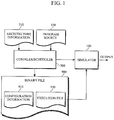
- FIG. 1 illustrates an example of a program development system that may be used to simulate a reconfigurable processor.
- the program development system includes a compiler/scheduler 300 and a simulator 100.
- the compiler/scheduler 300 reads architecture information 510 of a reconfigurable processor and a program source 530 that is to be executed based on the architecture information 510.
- the compiler/scheduler 300 compiles and schedules the architecture information 510 and program source 530 and then stores the results of the scheduling as an execution file 930 and configuration information 910 in a memory.
- the simulator 100 receives scheduling information from the compiler/scheduler 300, reads the configuration information 910 and execution file 930 from the memory, and simulates an execution of the execution file 930.
- the program development system may be included in a mobile device or a home device.
- the program development system may be included in a mobile terminal device, an embedded system, and the like.
- the simulator 100 may be used to simulate the processing performed by a single core processor or a multi-core processor.
- a binary file 900 transferred from the compiler/scheduler 300 to the simulator 100 includes configuration information 910 (or a configuration file) and an execution file 930.
- the architecture information 510 may include, for example, information regarding the architecture of functional units of the reconfigurable processor, a data architecture such as path interconnection data between the functional units, an architecture of control flow, and the like.
- the configuration information 910 may include information about how path interconnections between the functional units of the reconfigurable processor are structured to execute an application program.
- the execution file 930 may include instructions that are executed by the respective functional units in the reconfigurable processor based on the functional units having a fixed structure during a predetermined time period that is based on the configuration information 910.
- the configuration information 910 and instruction codes may be integrated with each other and handled together.
- configuration information and instruction codes that have to be processed in one clock cycle may be stored in memory in such a manner as to be adjacent to each other so that they may be simultaneously fetched by the processor.
- the simulator 100 may receive information related to scheduling from the compiler/scheduler 300.
- the scheduling information may be stored in the memory 900 and may be read by the simulator 100 from the memory 900.
- the simulator 100 may use an abstracted architecture model.
- the abstracted architecture model models operand routing paths between functional units as queues.
- the abstracted architecture may model routing paths between a functional unit which produces an operand and a functional unit which consumes the operand, instead of representing the operand routing paths using a sequence of actual interconnection logics. Accordingly, simulation speed may be enhanced because the number of interconnection components whose operations have to be checked in each simulation cycle is greatly reduced.
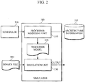
- FIG. 2 illustrates an example of a reconfigurable processor with a simulator.
- the simulator 100 includes a processor modeling unit 110 and a simulation unit 130.
- the processor modeling unit 110 models a processor by representing routing paths between a functional unit which produces an operand and a functional unit which consumes the operand, as a queue.
- the processor modeling unit 110 may model the processor based on information about routing delays between functional units and stage information of iteration loops based on modulo scheduling information received from a scheduler.
- the simulation unit 130 simulates a binary file received from a compiler.
- the simulation unit 130 simulates the binary file based on a processor model 113 produced by the processor modeling unit 110 and outputs the results of the simulation.
- the processor modeling unit 110 and the simulation unit 130 may be implemented in programs. Also, the processor model 113 and/or architecture information 510 may be data or a data structure stored in memory.
- the processor has interconnection logics between functional units that are sparse. As a result, there may be no direct path for routing a certain operand in one cycle between the functional units existing in an architecture. Accordingly, the CGRA processor generally utilizes two or more interconnection components to route one operand. For example, a value produced by a certain functional unit may pass through a register file, a multiplexer, other functional units, and the like, sequentially in order to be routed to the appropriate functional unit. Subsequently, the value may be transferred to a functional unit to consume the value.
- the scheduler of the CGRA processor may determine what operation has to be placed into each functional unit during a compile time. In addition, the CGRA processor may determine which chain of interconnection components has to be used to route operands between operations.
- the processor model 113 models operand routing paths between functional units, as a queue.
- the processor model 113 may model routing paths between a functional unit which produces an operand and a functional unit which consumes the operand, instead of addressing the operand routing path using a sequence of interconnection logics. For example, when an arbitrary operand is produced by a functional unit f1 at a time t1 and then consumed by a functional unit f2 at a time t2, a queue may be modeled which connects the destination port of the functional unit f1 at the t1 time to the source port of the functional unit f2 at the t2 time.
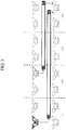
- FIG. 4 illustrates an example of a conventional architecture model.
- areas denoted by dotted lines are areas where no meaningful operands exist, areas filled in black illustrate the flow of an operand produced by the functional unit f1, and areas denoted by solid lines illustrate the flow of an operand produced by the functional unit f2.
- the functional units f1 through f4 may be Arithmetic Logical Units (ALUs) and a functional unit u1 may be a local register file.
- ALUs Arithmetic Logical Units
- a first operand produced by the functional unit f1 reaches an output buffer of the functional unit f1.
- the first operand reaches an input buffer of the functional unit u1 to be latched therein and simultaneously a second operand produced by the functional unit f2 reaches an output buffer of the functional unit f2.
- the first operand produced by the functional unit f1 reaches the output buffer of the functional unit u1 to be latched in the left input buffer of the functional unit f4
- the second operand produced by the functional unit f2 reaches the functional buffer of the functional unit u1 to be latched therein.
- the operand latched in the functional unit u1 reaches the output buffer of the functional unit u1 and is latched in the right input buffer of the functional unit f4.
- the first operand produced by the functional unit f1 at the time t reaches the functional unit f4 via the functional unit u1 at the time t+2 and is ready to be consumed.
- the second operand produced by the functional unit f2 at the time t+1 reaches the functional unit f4 via the functional unit u1 at the time t+3 and is ready to be consumed.
- the operations of the two operands are performed at the time t+3 by the functional unit f4.
- the first operand output by the functional unit f1 needs three clock cycles until the first operand is consumed in the functional unit f4, and the second operand output by the functional unit f2 needs two clock cycles until the operand is consumed in the functional unit f4. That is, the first operand is ready to be consumed at time t+2, but the first operand is not consumed until time t+3 when the second operand is also ready to be consumed.
- FIG. 5 illustrates an example of a modeling method that may be applied to a processor.
- the input buffers of the functional units f1 through f4 are omitted and the local register file (u1 of FIG. 4 ) is modeled as queues that have slots corresponding to a degree of delay.
- the operand routing queues exist for the purpose of transferring only meaningful operands.
- a simulator considers only queues corresponding to meaningful operands as interconnection components for routing the operands. By considering only meaningful operands, the number of interconnection components having to be considered every cycle is reduced, resulting in a reduction of a simulation time.
- the simulator simulates the processing of a reconfigurable processor array including four functional units.
- the reconfigurable processor array may include a plurality of functional units, for example, two units, four units, eight units, twelve units, sixteen units, twenty four units, or more.
- information about how the dataflow graph is mapped to the architecture may be used.
- the information may be supplied from a scheduler.
- the scheduler may produce scheduling information for a source operation and a destination operation of components that exist on a dataflow and may provide the scheduling information to the simulator.
- Scheduling for a CGRA processor may include a list scheduling framework and a Modulo scheduling framework.
- a routing queue may be implemented as a buffer. That is, a routing queue may be implemented by allowing a component which produces an operand to write a value in a buffer when producing the value, and allowing a component which consumes the operand to read the value from the buffer when consuming the value.
- Modulo scheduling corresponds to software pipelining.
- Modulo scheduling is a form of instruction scheduling that interleaves different iterations of a loop.
- Software pipelining improves performance by overlapping the execution of different iterations of a loop. An iteration can start executing before completions of previous iterations. The interval at which iterations are started is called the initiation interval.
- One goal of the software pipelining optimization is to find a schedule that overlaps iterations and uses the shortest possible initiation interval.
- the Modulo scheduling framework may produce an overlapped schedule in which a plurality of loop iterations are executed while overlapping.
- an iteration is divided into a plurality of stages and each stage has an execution cycle corresponding to the initiation interval.
- each initiation interval cycle operations corresponding to different stages from different loop iterations are scheduled in an overlapped manner. Consequently, for the Modulo scheduling framework, the schedule is produced so as to perform the same operation repeatedly included in different iterations at every initiation interval. Because the iterations of a loop are overlapped, and if the number of cycles consumed by the operand routing path exceeds the initiation interval, the value contained in the queue may be overwritten and may vanish before the component to consume the value can reach it
- FIG. 6 illustrates an example of modulo scheduling with a CGRA processor.
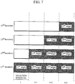
- FIG. 7 illustrates a processing flow of individual functional units f1 through f4 when the CGRA processor of FIG. 6 executes an iteration loop consisting of four stages.
- Each of the four functional units f1 through f4 illustrated in FIG. 6 is in charge of execution of one stage consisting of an iteration, and performs processing based on software pipelining to process data received from the previous stage and then output the processed data to the next stage.
- the functional unit f1 processes a first stage of a first iteration loop, and the functional units f2, f3, and f4 wait for the results of processing from the previous steps.
- the functional unit f1 processes a first stage of a second iteration loop
- the functional unit f2 receives the processing result on the first stage of the first iteration loop from the functional unit f1 and processes a second stage of the first iteration loop
- the functional units f3 and f4 continue to wait for the results of processing from the previous steps.
- the functional unit f1 processes a first stage of a third iteration loop
- the functional unit f2 receives the results of the processing on the first stage of the second iteration loop from the functional unit f1 and processes the second stage of the second iteration loop
- the functional unit f3 receives the results of the processing on the second stage of the first iteration loop from the functional unit f2 and processes a third stage of the first iteration loop
- the functional unit f4 continues to wait for the results of processing from the previous step.
- the functional unit f1 processes a first stage of a fourth iteration loop
- the functional unit f2 receives the results of the processing on the first stage of the third iteration loop from the functional unit f1 and processes a second stage of the third iteration loop
- the functional unit f3 receives the results of the processing on the second stage of the second iteration loop from the functional unit f2 and processes a third stage of the second iteration loop
- the functional unit f4 receives the results of the processing on the third stage of the first iteration from the functional unit f3 and processes the fourth stage of the first iteration loop.
- each clock cycle corresponds to an initiation interval.
- the first clock cycle corresponds to the first initiation interval
- the second clock cycle corresponds to the second initiation interval
- the third clock cycle corresponds to the third initiation interval
- the fourth clock cycle corresponds to the fourth initiation interval.
- a routing queue is implemented as a single buffer when simulating the results produced in the modulo scheduling framework using the processor model according to the current example, and if the number of cycles consumed by the operand routing path exceeds the initiation interval, the value contained in the queue is overwritten and vanishes before the component to consume the value can reach it. This is because the component which produces the operand writes a new value in the routing queue at every initiation interval.
- a queue defined by the processor modeling unit 110 may have a number of slots that corresponds to a ratio of a routing delay on the corresponding routing path and an initiation interval of a stage.
- the simulation unit 130 may write an operand produced in each functional unit in a first slot of the corresponding queue and may shift information recorded in each slot to a next slot at each initiation interval.
- a routing queue may be implemented to be as many slots as a number corresponding to a ceiling value.
- a ceiling value may be determined by dividing a routing delay by an initiation interval.
- the routing queue shifts a value recorded in a slot to a next slot at every initiation interval and a component which consumes the operand reads a value recorded in the final slot of the routing queue.
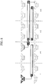
- FIG. 8 illustrates an example of a processor model 113 that may be applied to modulo-scheduled results.
- the initiation interval has been scheduled to be 2 cycles.
- the two operands shown in FIG. 8 both have routing delays greater than the initiation interval, a routing queue corresponding to each operand is divided into two slots.
- the simulation unit 130 shifts the previously produced value to the next slot of the corresponding routing queue when an initiation interval elapses.
- the simulation unit 130 may model operations for modulo-scheduled results.
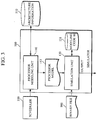
- FIG. 3 illustrates another example of a reconfigurable processor with a simulator.
- the simulator 100 may further include a modeling code data base (DB) 131 that stores host-oriented binary codes for operations of routing queues.
- the simulation unit 130 may read a binary file 900 and may extract a host-oriented binary code corresponding to the binary file 900 from the modeling code DB 131 to execute the host-oriented binary code, thereby performing a simulation.
- the simulator 100 may perform simulation by reconfiguring interconnections of routing queues from host-oriented binary codes extracted from the modeling code DB 131.
- a scheduler 330, a processor modeling unit 110, architecture information 510, and a processor model 113 correspond to elements with like reference numbers illustrated in FIG. 2 .
- Binary translation may be used to increase simulation speed by substituting a binary instruction of a machine targeted on a simulator with a binary code of a host machine performing the equivalent operation with the targeted machine. Accordingly, the substituted binary code of the host machine may be executed upon simulation of the equivalent code block.
- a CGRA processor may read configuration information from a specific address of a configuration memory at every cycle to perform an operation indicated by the configuration information of the corresponding cycle for each component. For example, a host binary code for configuration information may be produced for each address of a configuration memory. Thereafter, when simulation for configuration information existing at the same address of the configuration memory is performed, the simulation may be performed using the previously produced binary code.
- a binary translation technique is applied to the processor model 113.
- binary codes modeling the operations of routing queues are stored, instead of producing host binary codes to represent the behaviors of interconnection logics actually existing on processor architecture.
- binary codes modeling the operations of the routing queues may be stored instead of host binary codes related to the behaviors of interconnection logics existing in the real processor architecture.
- components whose operations are mapped into a data flow graph may be described as utilizing routing queues instead of being described as exchanging the produced or consumed value through interconnection logics.
- the shifting of values existing in routing queues to the next slots whenever an initiation interval elapses is all that needs to be modeled which leads to easy application of binary translation.
- the modeling code DB 131 may store a host binary code for configuration information in correspondence to each address of a configuration memory.
- the configuration information is information that describes the operations of routing queues between components on a dataflow graph.
- the simulation unit 130 may reconfigure a processor model 113 based on the host binary code read from the modeling code DB 131, and may read an execution file from a binary file 900 to perform simulation based on the reconfigured processor model 113.
- the abstracted architecture model can be considered an architecture graph resulting from modeling actual architecture and a dataflow graph.
- each edge existing on a dataflow graph may be modeled as a queue.
- the abstracted architecture model may be used to abstract components to which edges of a dataflow graph are mapped, as queues, while maintaining components such as functional units, constant units, and the like, to which nodes of the dataflow graph are mapped in actual architecture. In doing so, interconnection components having little or no influence on operation of applications may be removed and the sequences of interconnection components used to route an operand corresponding to a dataflow edge may be simplified.
- the method of simulating a reconfigurable processor includes an operation of modeling a processor by representing routing paths between functional units as queues.
- the modeling may route paths of functional units which produce operands and functional units which consume the operands based on information about routing delays between functional units and stage information of iteration loops according to modulo scheduling received from a scheduler.
- a simulation of a binary file received from a compiler based on the processor model produced in the processor modeling may be performed and the results of the simulation may be output.
- a queue defined in the processor modeling may have a number of slots that corresponds to a ratio of a routing delay on the corresponding routing path and an initiation interval of a stage.
- an operand produced in each functional unit is written in the first slot of the corresponding queue and information written in each slot is shifted to an adjacent slot at each initiation interval.
- the stage information includes stage division information of an iteration and specific information about the relationship between functional units assigned to individual stages, functional units which produce operands, and functional units which consume the operands.
- the binary file received from the compiler may include a configuration file and an execution file.
- simulation may be performed by reading a binary file and executing a host-oriented binary code corresponding to the binary file, extracted from a modeling code DB which stores host-oriented binary codes for operations of routing queues.
- the processes, functions, methods, and/or software described above may be recorded, stored, or fixed in one or more computer-readable storage media that includes program instructions to be implemented by a computer to cause a processor to execute or perform the program instructions.
- the media may also include, alone or in combination with the program instructions, data files, data structures, and the like.
- Examples of computer-readable storage media include magnetic media, such as hard disks, floppy disks, and magnetic tape; optical media such as CD ROM disks and DVDs; magneto-optical media, such as optical disks; and hardware devices that are specially configured to store and perform program instructions, such as read-only memory (ROM), random access memory (RAM), flash memory, and the like.
- Examples of program instructions include machine code, such as produced by a compiler, and files containing higher level code that may be executed by the computer using an interpreter.
- the described hardware devices may be configured to act as one or more software modules in order to perform the operations and methods described above, or vice versa.
- a computer-readable storage medium may be distributed among computer systems connected through a network and computer-readable codes or program instructions may be stored and executed in a decentralized manner.
- the terminal device described herein may refer to mobile devices such as a cellular phone, a personal digital assistant (PDA), a digital camera, a portable game console, an MP3 player, a portable/personal multimedia player (PMP), a handheld e-book, a portable lab-top personal computer (PC), a global positioning system (GPS) navigation, and devices such as a desktop PC, a high definition television (HDTV), an optical disc player, a setup box, and the like, capable of wireless communication or network communication consistent with that disclosed herein.
- mobile devices such as a cellular phone, a personal digital assistant (PDA), a digital camera, a portable game console, an MP3 player, a portable/personal multimedia player (PMP), a handheld e-book, a portable lab-top personal computer (PC), a global positioning system (GPS) navigation, and devices such as a desktop PC, a high definition television (HDTV), an optical disc player, a setup box, and the like, capable of wireless communication or network communication consistent with that disclosed herein
- a computing system or a computer may include a microprocessor that is electrically connected with a bus, a user interface, and a memory controller. It may further include a flash memory device. The flash memory device may store N-bit data via the memory controller. The N-bit data is processed or will be processed by the microprocessor and N may be 1 or an integer greater than 1. Where the computing system or computer is a mobile apparatus, a battery may be additionally provided to supply operation voltage of the computing system or computer.
- the computing system or computer may further include an application chipset, a camera image processor (CIS), a mobile Dynamic Random Access Memory (DRAM), and the like.
- the memory controller and the flash memory device may constitute a solid state drive/disk (SSD) that uses a non-volatile memory to store data.
- SSD solid state drive/disk
Landscapes
- Engineering & Computer Science (AREA)
- Theoretical Computer Science (AREA)
- Computer Hardware Design (AREA)
- Physics & Mathematics (AREA)
- General Engineering & Computer Science (AREA)
- General Physics & Mathematics (AREA)
- Software Systems (AREA)
- Evolutionary Computation (AREA)
- Geometry (AREA)
- Computer Networks & Wireless Communication (AREA)
- Design And Manufacture Of Integrated Circuits (AREA)
- Debugging And Monitoring (AREA)
- Stored Programmes (AREA)
- Test And Diagnosis Of Digital Computers (AREA)
- Devices For Executing Special Programs (AREA)
Claims (8)
- Simulator (100) eines rekonfigurierbaren Prozessors, wobei der Simulator umfasst:eine Prozessor-Modellierungseinheit (110) zur Erzeugung eines Prozessormodells (113), das eine Warteschlange umfasst, welche einen Routingpfad zwischen einer funktionalen Einheit, die ein Operand erzeugt, und einer funktionalen Einheit, die das Operand konsumiert, darstellt, wobei das Prozessormodell (113) auf Routingverzögerungen zwischen den funktionalen Einheiten undStufeninformationen von Iterationsschleifen basierend auf Modulo-Scheduling basiert, und die Warteschlange eine Anzahl von Slots aufweist, die mit einem Verhältnis einer Routingverzögerung auf dem Routingpfad und mit einem Initiationsintervall einer Stufe korrespondieren; undeine Simulierungseinheit (130) zur Simulierung einer binären Datei (900), die aus einem Compiler (300) basierend auf dem von der Prozessor-Modellierungseinheit (110) erzeugten Prozessormodell (113) empfangenen wird, und zur Ausgabe der Ergebnisse der Simulation, wobei die Simulierungseinheit (130) ein Operand, das in jeder funktionalen Einheit erzeugt wurde, in einen ersten Slot einer korrespondierenden Warteschlange schreibt, und die in jedem Slot geschriebenen Informationen bei jedem Initiationsintervall in einen nächsten Slot verschiebt.
- Simulator (100) gemäß Anspruch 1, wobei die aus dem Compiler (300) empfangene binäre Datei (900) eine Konfigurationsdatei (910) und eine Ausführungsdatei (930) umfasst.
- Simulator (100) gemäß Anspruch 1, weiterhin umfassend eine Datenbank für Modellierungscodes, um Host-orientierte Binärcodes für Operationen der Routing-Warteschlangen zu speichern,
wobei die Simulierungseinheit (130) die Simulierung durch Re-Konfigurieren der Verbindungen zwischen Routing-Warteschlangen aus den aus der Datenbank für Modellierungscodes extrahierten Host-orientierten Binärcodes durchführt. - Simulierungsverfahren eines rekonfigurierbaren Prozessors, wobei das Verfahren umfasst:Erzeugen eines Prozessormodells (113), das eine Warteschlange umfasst, welche einen Routingpfad zwischen einer funktionalen Einheit, die ein Operand erzeugt, und einer funktionalen Einheit, die das Operand konsumiert, darstellt, wobei das Prozessormodell (113) auf Routingverzögerungen zwischen den funktionalen Einheiten und Stufeninformationen von Iterationsschleifen basierend auf Modulo-Scheduling basiert; undSimulieren einer binären Datei (900), die aus einem Compiler (300) basierend auf dem von der Prozessor-Modellierungseinheit (110) erzeugten Prozessormodell (113) empfangenen wird, und Ausgeben des Ergebnisses der Simulation,wobei die bei der Erzeugung des Prozessormodells (113) dargestellte Warteschlange eine Anzahl von Slots aufweist, die mit einem Verhältnis einer Routingverzögerung auf dem Routingpfad und mit einem Initiationsintervall einer Stufe korrespondieren, und wobei die Simulierung der binären Datei (900) das Schreiben eines Operands, das in jeder funktionalen Einheit erzeugt wurde, in einen ersten Slot einer korrespondierenden Warteschlange, und das Verschieben der in jeden Slot geschriebenen Informationen bei jedem Initiationsintervall in einen nächsten Slot umfasst.
- Simulierungsverfahren gemäß Anspruch 4, wobei die Stufeninformationen Stufenteilungsinformationen zu einer Iteration sowie Informationen über die Beziehung zwischen den funktionalen Einheiten, die den individuellen Stufen zugewiesen sind, den funktionalen Einheiten, die Operanden erzeugen, und den funktionalen Einheiten, die Operanden konsumieren, umfassen.
- Simulierungsverfahren gemäß Anspruch 4, wobei die aus dem Compiler (300) empfangene binäre Datei (900) eine Konfigurationsdatei (910) und eine Ausführungsdatei (930) umfasst.
- Simulierungsverfahren gemäß Anspruch 4, wobei das Simulieren der binären Datei (900) umfasst: Durchführen einer Simulierung durch Lesen der binären Datei (900), Extrahieren eines mit der binären Datei (900) korrespondierenden Host-orientierten Binärcodes aus einer Datenbank für Modellierungscodes, welche Host-orientierte Binärcodes für Operationen von Routing-Warteschlangen speichert, und Ausführen des Host-orientierten Binärcodes.
- Computerlesbares Speichermedium, auf dem Programmanweisungen gespeichert sind, um einen Prozessor zu veranlassen, ein Simulierungsverfahren eines rekonfigurierbaren Prozessors umzusetzen, wobei das Simulierungsverfahren umfasst:Erzeugen eines Prozessormodells (113), das eine Warteschlange umfasst, welche einen Routingpfad zwischen einer funktionalen Einheit, die ein Operand erzeugt, und einer funktionalen Einheit, die das Operand konsumiert, darstellt, wobei das Prozessormodell (113) auf Routingverzögerungen zwischen den funktionalen Einheiten und Stufeninformationen von Iterationsschleifen basierend auf Modulo-Scheduling basiert; undSimulieren einer binären Datei (900), die aus einem Compiler (300) basierend auf dem erzeugten Prozessormodell (113) empfangenen wird und Ausgeben des Ergebnisses der Simulation,wobei die bei der Erzeugung des Prozessormodells (113) dargestellte Warteschlange eine Anzahl von Slots aufweist, die mit einem Verhältnis einer Routingverzögerung auf dem Routingpfad und mit einem Initiationsintervall einer Stufe korrespondieren; undwobei die Simulierung der binären Datei (900) das Schreiben eines Operands, das in jeder funktionalen Einheit erzeugt wurde, in einen ersten Slot einer korrespondierenden Warteschlange, und das Verschieben der in jeden Slot geschriebenen Informationen bei jedem Initiationsintervall in einen nächsten Slot umfasst.
Applications Claiming Priority (1)
| Application Number | Priority Date | Filing Date | Title |
|---|---|---|---|
| KR1020100029379A KR101647817B1 (ko) | 2010-03-31 | 2010-03-31 | 재구성 가능한 프로세서의 시뮬레이션 장치 및 방법 |
Publications (2)
| Publication Number | Publication Date |
|---|---|
| EP2372587A1 EP2372587A1 (de) | 2011-10-05 |
| EP2372587B1 true EP2372587B1 (de) | 2016-12-28 |
Family
ID=44121730
Family Applications (1)
| Application Number | Title | Priority Date | Filing Date |
|---|---|---|---|
| EP11154723.8A Active EP2372587B1 (de) | 2010-03-31 | 2011-02-16 | Vorrichtung und Verfahren zur Simulierung eines rekonfigurierbaren Prozessors |
Country Status (5)
| Country | Link |
|---|---|
| US (1) | US8725486B2 (de) |
| EP (1) | EP2372587B1 (de) |
| JP (1) | JP5797438B2 (de) |
| KR (1) | KR101647817B1 (de) |
| CN (1) | CN102207904B (de) |
Families Citing this family (10)
| Publication number | Priority date | Publication date | Assignee | Title |
|---|---|---|---|---|
| US10983947B2 (en) * | 2011-11-21 | 2021-04-20 | Robert Keith Mykland | Method and dynamically reconfigurable processor adapted for management of persistence of information across multiple instruction cycles |
| KR101926464B1 (ko) * | 2012-10-11 | 2018-12-07 | 삼성전자 주식회사 | 멀티코어 프로세서에서 수행되는 프로그램의 컴파일 방법, 멀티코어 프로세서의 태스크 매핑 방법 및 태스크 스케줄링 방법 |
| KR101962250B1 (ko) * | 2013-03-05 | 2019-03-26 | 삼성전자주식회사 | 재구성가능 아키텍처를 위한 스케줄러 및 스케줄링 방법 |
| KR20140126190A (ko) * | 2013-04-22 | 2014-10-30 | 삼성전자주식회사 | 프로세서의 긴 라우팅 처리를 지원하는 메모리 장치, 그 메모리 장치를 이용한 스케줄링 장치 및 방법 |
| KR102204282B1 (ko) * | 2013-11-25 | 2021-01-18 | 삼성전자주식회사 | 다수의 기능 유닛을 가지는 프로세서를 위한 루프 스케쥴링 방법 |
| US11010505B2 (en) | 2015-12-01 | 2021-05-18 | International Business Machines Corporation | Simulation of virtual processors |
| US10996970B2 (en) * | 2017-12-14 | 2021-05-04 | Samsung Electronics Co., Ltd. | Method for data center storage evaluation framework simulation |
| CN109471636B (zh) * | 2018-09-14 | 2020-07-14 | 上海交通大学 | 粗粒度可重构体系结构的算子映射方法及系统 |
| US11709664B2 (en) | 2020-06-02 | 2023-07-25 | SambaNova Systems, Inc. | Anti-congestion flow control for reconfigurable processors |
| US11237971B1 (en) * | 2020-09-16 | 2022-02-01 | SambaNova Systems, Inc. | Compile time logic for detecting streaming compatible and broadcast compatible data access patterns |
Family Cites Families (19)
| Publication number | Priority date | Publication date | Assignee | Title |
|---|---|---|---|---|
| US5841967A (en) | 1996-10-17 | 1998-11-24 | Quickturn Design Systems, Inc. | Method and apparatus for design verification using emulation and simulation |
| US6766284B2 (en) * | 1998-04-10 | 2004-07-20 | Peter Finch | Method and apparatus for generating co-simulation and production executables from a single source |
| US6421808B1 (en) * | 1998-04-24 | 2002-07-16 | Cadance Design Systems, Inc. | Hardware design language for the design of integrated circuits |
| US20010025363A1 (en) * | 2000-03-24 | 2001-09-27 | Cary Ussery | Designer configurable multi-processor system |
| AU2001266660A1 (en) * | 2000-06-02 | 2001-12-17 | Virtio Corporation | Method and system for virtual prototyping |
| US7054802B2 (en) | 2000-10-20 | 2006-05-30 | Quickturn Design Systems, Inc. | Hardware-assisted design verification system using a packet-based protocol logic synthesized for efficient data loading and unloading |
| US20020133325A1 (en) | 2001-02-09 | 2002-09-19 | Hoare Raymond R. | Discrete event simulator |
| US20030149962A1 (en) | 2001-11-21 | 2003-08-07 | Willis John Christopher | Simulation of designs using programmable processors and electronically re-configurable logic arrays |
| US7366651B1 (en) | 2003-03-14 | 2008-04-29 | Xilinx, Inc. | Co-simulation interface |
| US7234125B1 (en) * | 2003-06-23 | 2007-06-19 | Altera Corporation | Timing analysis for programmable logic |
| EP1530137A1 (de) | 2003-11-10 | 2005-05-11 | Robert Bosch Gmbh | Simulationssystem und Computerimplementiertes Verfahren zur Simulation und Verifikation von Kontrollsystemen |
| US7698118B2 (en) * | 2004-04-15 | 2010-04-13 | Mentor Graphics Corporation | Logic design modeling and interconnection |
| US20060277020A1 (en) | 2005-06-02 | 2006-12-07 | Tharas Systems | A reconfigurable system for verification of electronic circuits using high-speed serial links to connect asymmetrical evaluation and canvassing instruction processors |
| US7380232B1 (en) * | 2006-03-10 | 2008-05-27 | Xilinx, Inc. | Method and apparatus for designing a system for implementation in a programmable logic device |
| GB0605349D0 (en) * | 2006-03-17 | 2006-04-26 | Imec Inter Uni Micro Electr | Reconfigurable multi-processing coarse-grain array |
| KR100813662B1 (ko) * | 2006-11-17 | 2008-03-14 | 삼성전자주식회사 | 프로세서 구조 및 응용의 최적화를 위한 프로파일러 |
| US8265917B1 (en) * | 2008-02-25 | 2012-09-11 | Xilinx, Inc. | Co-simulation synchronization interface for IC modeling |
| US7979759B2 (en) * | 2009-01-08 | 2011-07-12 | International Business Machines Corporation | Test and bring-up of an enhanced cascade interconnect memory system |
| KR101635397B1 (ko) * | 2010-03-03 | 2016-07-04 | 삼성전자주식회사 | 재구성 가능한 프로세서 코어를 사용하는 멀티코어 시스템의 시뮬레이터 및 시뮬레이션 방법 |
-
2010
- 2010-03-31 KR KR1020100029379A patent/KR101647817B1/ko active Active
-
2011
- 2011-01-25 US US13/012,945 patent/US8725486B2/en active Active
- 2011-02-16 EP EP11154723.8A patent/EP2372587B1/de active Active
- 2011-03-30 JP JP2011076608A patent/JP5797438B2/ja active Active
- 2011-03-31 CN CN201110089956.XA patent/CN102207904B/zh active Active
Non-Patent Citations (1)
| Title |
|---|
| None * |
Also Published As
| Publication number | Publication date |
|---|---|
| KR101647817B1 (ko) | 2016-08-24 |
| JP2011216092A (ja) | 2011-10-27 |
| US20110246170A1 (en) | 2011-10-06 |
| EP2372587A1 (de) | 2011-10-05 |
| JP5797438B2 (ja) | 2015-10-21 |
| US8725486B2 (en) | 2014-05-13 |
| CN102207904B (zh) | 2019-03-29 |
| KR20110109590A (ko) | 2011-10-06 |
| CN102207904A (zh) | 2011-10-05 |
Similar Documents
| Publication | Publication Date | Title |
|---|---|---|
| US8725486B2 (en) | Apparatus and method for simulating a reconfigurable processor | |
| Staunstrup et al. | Hardware/software co-design: principles and practice | |
| CN104657210B (zh) | 针对具有多个功能单元的处理器调度循环的方法 | |
| US9734058B2 (en) | Optimizing configuration memory by sequentially mapping the generated configuration data by determining regular encoding is possible and functional units are the same in adjacent cycles | |
| CN104424026B (zh) | 一种指令调度方法及装置 | |
| KR101715986B1 (ko) | 신호 흐름이 프로그램된 디지털 신호 프로세서 코드의 효율적인 자원 관리를 위한 시스템 및 방법 | |
| CN105930201A (zh) | 一种可重构专用处理器核的功能模拟器 | |
| US20170364473A1 (en) | Program counter alignment across a reconfigurable hum fabric | |
| JP7476299B2 (ja) | 同期プロセッサのためのコンパイル | |
| US7228513B2 (en) | Circuit operation verification device and method | |
| Yang et al. | An approach to build cycle accurate full system VLIW simulation platform | |
| US7162403B2 (en) | System and method for efficiently tracing simulation data in hardware acceleration simulation systems | |
| US8601415B2 (en) | Planning for hardware-accelerated functional verification | |
| US20240362024A1 (en) | Schedule Instructions of a Program of Data Flows for Execution in Tiles of a Coarse Grained Reconfigurable Array | |
| KR102325612B1 (ko) | 시뮬레이터를 구현하는 방법, 장치, 기기 및 매체 | |
| CN118171707B (zh) | 一种基于卷积神经网络微处理器的虚拟原型平台 | |
| Tang et al. | Pipe-DBT: enhancing dynamic binary translation simulators to support pipeline-level simulation | |
| JP2001256048A (ja) | データ処理装置のシミュレーション | |
| US9141498B2 (en) | Method for verification of reconfigurable processor | |
| Ruggiero et al. | Reducing the abstraction and optimality gaps in the allocation and scheduling for variable voltage/frequency MPSoC platforms | |
| US9087152B2 (en) | Verification supporting apparatus and verification supporting method of reconfigurable processor | |
| CN119938430A (zh) | 一种流水级指令的原型验证方法、装置、设备及介质 | |
| KR102044784B1 (ko) | 재구성 프로세서에서 충돌 해결을 가속화하기 위한 방법 및 시스템 | |
| CN102855206B (zh) | 一种数据流及其与控制流的交互方法和设备 | |
| CN118364756A (zh) | 验证系统、验证方法、电子设备和存储介质 |
Legal Events
| Date | Code | Title | Description |
|---|---|---|---|
| PUAI | Public reference made under article 153(3) epc to a published international application that has entered the european phase |
Free format text: ORIGINAL CODE: 0009012 |
|
| AK | Designated contracting states |
Kind code of ref document: A1 Designated state(s): AL AT BE BG CH CY CZ DE DK EE ES FI FR GB GR HR HU IE IS IT LI LT LU LV MC MK MT NL NO PL PT RO RS SE SI SK SM TR |
|
| AX | Request for extension of the european patent |
Extension state: BA ME |
|
| 17P | Request for examination filed |
Effective date: 20120321 |
|
| RAP1 | Party data changed (applicant data changed or rights of an application transferred) |
Owner name: SAMSUNG ELECTRONICS CO., LTD. |
|
| GRAP | Despatch of communication of intention to grant a patent |
Free format text: ORIGINAL CODE: EPIDOSNIGR1 |
|
| RIC1 | Information provided on ipc code assigned before grant |
Ipc: G06F 17/50 20060101AFI20160615BHEP |
|
| INTG | Intention to grant announced |
Effective date: 20160712 |
|
| GRAS | Grant fee paid |
Free format text: ORIGINAL CODE: EPIDOSNIGR3 |
|
| GRAA | (expected) grant |
Free format text: ORIGINAL CODE: 0009210 |
|
| AK | Designated contracting states |
Kind code of ref document: B1 Designated state(s): AL AT BE BG CH CY CZ DE DK EE ES FI FR GB GR HR HU IE IS IT LI LT LU LV MC MK MT NL NO PL PT RO RS SE SI SK SM TR |
|
| REG | Reference to a national code |
Ref country code: GB Ref legal event code: FG4D |
|
| REG | Reference to a national code |
Ref country code: CH Ref legal event code: EP |
|
| REG | Reference to a national code |
Ref country code: AT Ref legal event code: REF Ref document number: 857862 Country of ref document: AT Kind code of ref document: T Effective date: 20170115 |
|
| REG | Reference to a national code |
Ref country code: IE Ref legal event code: FG4D |
|
| REG | Reference to a national code |
Ref country code: DE Ref legal event code: R096 Ref document number: 602011033766 Country of ref document: DE |
|
| REG | Reference to a national code |
Ref country code: FR Ref legal event code: PLFP Year of fee payment: 7 |
|
| PG25 | Lapsed in a contracting state [announced via postgrant information from national office to epo] |
Ref country code: LV Free format text: LAPSE BECAUSE OF FAILURE TO SUBMIT A TRANSLATION OF THE DESCRIPTION OR TO PAY THE FEE WITHIN THE PRESCRIBED TIME-LIMIT Effective date: 20161228 |
|
| REG | Reference to a national code |
Ref country code: LT Ref legal event code: MG4D |
|
| PG25 | Lapsed in a contracting state [announced via postgrant information from national office to epo] |
Ref country code: SE Free format text: LAPSE BECAUSE OF FAILURE TO SUBMIT A TRANSLATION OF THE DESCRIPTION OR TO PAY THE FEE WITHIN THE PRESCRIBED TIME-LIMIT Effective date: 20161228 Ref country code: GR Free format text: LAPSE BECAUSE OF FAILURE TO SUBMIT A TRANSLATION OF THE DESCRIPTION OR TO PAY THE FEE WITHIN THE PRESCRIBED TIME-LIMIT Effective date: 20170329 Ref country code: LT Free format text: LAPSE BECAUSE OF FAILURE TO SUBMIT A TRANSLATION OF THE DESCRIPTION OR TO PAY THE FEE WITHIN THE PRESCRIBED TIME-LIMIT Effective date: 20161228 Ref country code: NO Free format text: LAPSE BECAUSE OF FAILURE TO SUBMIT A TRANSLATION OF THE DESCRIPTION OR TO PAY THE FEE WITHIN THE PRESCRIBED TIME-LIMIT Effective date: 20170328 |
|
| REG | Reference to a national code |
Ref country code: NL Ref legal event code: MP Effective date: 20161228 |
|
| REG | Reference to a national code |
Ref country code: AT Ref legal event code: MK05 Ref document number: 857862 Country of ref document: AT Kind code of ref document: T Effective date: 20161228 |
|
| PG25 | Lapsed in a contracting state [announced via postgrant information from national office to epo] |
Ref country code: HR Free format text: LAPSE BECAUSE OF FAILURE TO SUBMIT A TRANSLATION OF THE DESCRIPTION OR TO PAY THE FEE WITHIN THE PRESCRIBED TIME-LIMIT Effective date: 20161228 Ref country code: RS Free format text: LAPSE BECAUSE OF FAILURE TO SUBMIT A TRANSLATION OF THE DESCRIPTION OR TO PAY THE FEE WITHIN THE PRESCRIBED TIME-LIMIT Effective date: 20161228 Ref country code: FI Free format text: LAPSE BECAUSE OF FAILURE TO SUBMIT A TRANSLATION OF THE DESCRIPTION OR TO PAY THE FEE WITHIN THE PRESCRIBED TIME-LIMIT Effective date: 20161228 Ref country code: BE Free format text: LAPSE BECAUSE OF NON-PAYMENT OF DUE FEES Effective date: 20170228 |
|
| PG25 | Lapsed in a contracting state [announced via postgrant information from national office to epo] |
Ref country code: NL Free format text: LAPSE BECAUSE OF FAILURE TO SUBMIT A TRANSLATION OF THE DESCRIPTION OR TO PAY THE FEE WITHIN THE PRESCRIBED TIME-LIMIT Effective date: 20161228 |
|
| PG25 | Lapsed in a contracting state [announced via postgrant information from national office to epo] |
Ref country code: SK Free format text: LAPSE BECAUSE OF FAILURE TO SUBMIT A TRANSLATION OF THE DESCRIPTION OR TO PAY THE FEE WITHIN THE PRESCRIBED TIME-LIMIT Effective date: 20161228 Ref country code: EE Free format text: LAPSE BECAUSE OF FAILURE TO SUBMIT A TRANSLATION OF THE DESCRIPTION OR TO PAY THE FEE WITHIN THE PRESCRIBED TIME-LIMIT Effective date: 20161228 Ref country code: RO Free format text: LAPSE BECAUSE OF FAILURE TO SUBMIT A TRANSLATION OF THE DESCRIPTION OR TO PAY THE FEE WITHIN THE PRESCRIBED TIME-LIMIT Effective date: 20161228 Ref country code: IS Free format text: LAPSE BECAUSE OF FAILURE TO SUBMIT A TRANSLATION OF THE DESCRIPTION OR TO PAY THE FEE WITHIN THE PRESCRIBED TIME-LIMIT Effective date: 20170428 Ref country code: CZ Free format text: LAPSE BECAUSE OF FAILURE TO SUBMIT A TRANSLATION OF THE DESCRIPTION OR TO PAY THE FEE WITHIN THE PRESCRIBED TIME-LIMIT Effective date: 20161228 |
|
| PG25 | Lapsed in a contracting state [announced via postgrant information from national office to epo] |
Ref country code: AT Free format text: LAPSE BECAUSE OF FAILURE TO SUBMIT A TRANSLATION OF THE DESCRIPTION OR TO PAY THE FEE WITHIN THE PRESCRIBED TIME-LIMIT Effective date: 20161228 Ref country code: IT Free format text: LAPSE BECAUSE OF FAILURE TO SUBMIT A TRANSLATION OF THE DESCRIPTION OR TO PAY THE FEE WITHIN THE PRESCRIBED TIME-LIMIT Effective date: 20161228 Ref country code: BE Free format text: LAPSE BECAUSE OF FAILURE TO SUBMIT A TRANSLATION OF THE DESCRIPTION OR TO PAY THE FEE WITHIN THE PRESCRIBED TIME-LIMIT Effective date: 20161228 Ref country code: SM Free format text: LAPSE BECAUSE OF FAILURE TO SUBMIT A TRANSLATION OF THE DESCRIPTION OR TO PAY THE FEE WITHIN THE PRESCRIBED TIME-LIMIT Effective date: 20161228 Ref country code: ES Free format text: LAPSE BECAUSE OF FAILURE TO SUBMIT A TRANSLATION OF THE DESCRIPTION OR TO PAY THE FEE WITHIN THE PRESCRIBED TIME-LIMIT Effective date: 20161228 Ref country code: PL Free format text: LAPSE BECAUSE OF FAILURE TO SUBMIT A TRANSLATION OF THE DESCRIPTION OR TO PAY THE FEE WITHIN THE PRESCRIBED TIME-LIMIT Effective date: 20161228 Ref country code: BG Free format text: LAPSE BECAUSE OF FAILURE TO SUBMIT A TRANSLATION OF THE DESCRIPTION OR TO PAY THE FEE WITHIN THE PRESCRIBED TIME-LIMIT Effective date: 20170328 Ref country code: PT Free format text: LAPSE BECAUSE OF FAILURE TO SUBMIT A TRANSLATION OF THE DESCRIPTION OR TO PAY THE FEE WITHIN THE PRESCRIBED TIME-LIMIT Effective date: 20170428 |
|
| PG25 | Lapsed in a contracting state [announced via postgrant information from national office to epo] |
Ref country code: MC Free format text: LAPSE BECAUSE OF FAILURE TO SUBMIT A TRANSLATION OF THE DESCRIPTION OR TO PAY THE FEE WITHIN THE PRESCRIBED TIME-LIMIT Effective date: 20161228 |
|
| REG | Reference to a national code |
Ref country code: CH Ref legal event code: PL Ref country code: DE Ref legal event code: R097 Ref document number: 602011033766 Country of ref document: DE |
|
| PG25 | Lapsed in a contracting state [announced via postgrant information from national office to epo] |
Ref country code: CH Free format text: LAPSE BECAUSE OF NON-PAYMENT OF DUE FEES Effective date: 20170228 Ref country code: LI Free format text: LAPSE BECAUSE OF NON-PAYMENT OF DUE FEES Effective date: 20170228 |
|
| PLBE | No opposition filed within time limit |
Free format text: ORIGINAL CODE: 0009261 |
|
| STAA | Information on the status of an ep patent application or granted ep patent |
Free format text: STATUS: NO OPPOSITION FILED WITHIN TIME LIMIT |
|
| REG | Reference to a national code |
Ref country code: IE Ref legal event code: MM4A |
|
| PG25 | Lapsed in a contracting state [announced via postgrant information from national office to epo] |
Ref country code: DK Free format text: LAPSE BECAUSE OF FAILURE TO SUBMIT A TRANSLATION OF THE DESCRIPTION OR TO PAY THE FEE WITHIN THE PRESCRIBED TIME-LIMIT Effective date: 20161228 |
|
| 26N | No opposition filed |
Effective date: 20170929 |
|
| PG25 | Lapsed in a contracting state [announced via postgrant information from national office to epo] |
Ref country code: LU Free format text: LAPSE BECAUSE OF NON-PAYMENT OF DUE FEES Effective date: 20170216 |
|
| REG | Reference to a national code |
Ref country code: FR Ref legal event code: PLFP Year of fee payment: 8 |
|
| PG25 | Lapsed in a contracting state [announced via postgrant information from national office to epo] |
Ref country code: IE Free format text: LAPSE BECAUSE OF NON-PAYMENT OF DUE FEES Effective date: 20170216 Ref country code: SI Free format text: LAPSE BECAUSE OF FAILURE TO SUBMIT A TRANSLATION OF THE DESCRIPTION OR TO PAY THE FEE WITHIN THE PRESCRIBED TIME-LIMIT Effective date: 20161228 |
|
| PG25 | Lapsed in a contracting state [announced via postgrant information from national office to epo] |
Ref country code: MT Free format text: LAPSE BECAUSE OF NON-PAYMENT OF DUE FEES Effective date: 20170216 |
|
| PG25 | Lapsed in a contracting state [announced via postgrant information from national office to epo] |
Ref country code: HU Free format text: LAPSE BECAUSE OF FAILURE TO SUBMIT A TRANSLATION OF THE DESCRIPTION OR TO PAY THE FEE WITHIN THE PRESCRIBED TIME-LIMIT; INVALID AB INITIO Effective date: 20110216 |
|
| PG25 | Lapsed in a contracting state [announced via postgrant information from national office to epo] |
Ref country code: CY Free format text: LAPSE BECAUSE OF NON-PAYMENT OF DUE FEES Effective date: 20161228 |
|
| REG | Reference to a national code |
Ref country code: DE Ref legal event code: R079 Ref document number: 602011033766 Country of ref document: DE Free format text: PREVIOUS MAIN CLASS: G06F0017500000 Ipc: G06F0030000000 |
|
| PG25 | Lapsed in a contracting state [announced via postgrant information from national office to epo] |
Ref country code: MK Free format text: LAPSE BECAUSE OF FAILURE TO SUBMIT A TRANSLATION OF THE DESCRIPTION OR TO PAY THE FEE WITHIN THE PRESCRIBED TIME-LIMIT Effective date: 20161228 |
|
| PG25 | Lapsed in a contracting state [announced via postgrant information from national office to epo] |
Ref country code: TR Free format text: LAPSE BECAUSE OF FAILURE TO SUBMIT A TRANSLATION OF THE DESCRIPTION OR TO PAY THE FEE WITHIN THE PRESCRIBED TIME-LIMIT Effective date: 20161228 |
|
| PG25 | Lapsed in a contracting state [announced via postgrant information from national office to epo] |
Ref country code: AL Free format text: LAPSE BECAUSE OF FAILURE TO SUBMIT A TRANSLATION OF THE DESCRIPTION OR TO PAY THE FEE WITHIN THE PRESCRIBED TIME-LIMIT Effective date: 20161228 |
|
| P01 | Opt-out of the competence of the unified patent court (upc) registered |
Effective date: 20230530 |
|
| PGFP | Annual fee paid to national office [announced via postgrant information from national office to epo] |
Ref country code: GB Payment date: 20260112 Year of fee payment: 16 |
|
| PGFP | Annual fee paid to national office [announced via postgrant information from national office to epo] |
Ref country code: DE Payment date: 20260114 Year of fee payment: 16 |
|
| PGFP | Annual fee paid to national office [announced via postgrant information from national office to epo] |
Ref country code: FR Payment date: 20260108 Year of fee payment: 16 |