EP2371606A2 - Shift Lever Device - Google Patents
Shift Lever Device Download PDFInfo
- Publication number
- EP2371606A2 EP2371606A2 EP11160019A EP11160019A EP2371606A2 EP 2371606 A2 EP2371606 A2 EP 2371606A2 EP 11160019 A EP11160019 A EP 11160019A EP 11160019 A EP11160019 A EP 11160019A EP 2371606 A2 EP2371606 A2 EP 2371606A2
- Authority
- EP
- European Patent Office
- Prior art keywords
- circuit board
- electric component
- board
- shift lever
- body case
- Prior art date
- Legal status (The legal status is an assumption and is not a legal conclusion. Google has not performed a legal analysis and makes no representation as to the accuracy of the status listed.)
- Withdrawn
Links
Images


Classifications
-
- B—PERFORMING OPERATIONS; TRANSPORTING
- B60—VEHICLES IN GENERAL
- B60K—ARRANGEMENT OR MOUNTING OF PROPULSION UNITS OR OF TRANSMISSIONS IN VEHICLES; ARRANGEMENT OR MOUNTING OF PLURAL DIVERSE PRIME-MOVERS IN VEHICLES; AUXILIARY DRIVES FOR VEHICLES; INSTRUMENTATION OR DASHBOARDS FOR VEHICLES; ARRANGEMENTS IN CONNECTION WITH COOLING, AIR INTAKE, GAS EXHAUST OR FUEL SUPPLY OF PROPULSION UNITS IN VEHICLES
- B60K20/00—Arrangement or mounting of change-speed gearing control devices in vehicles
- B60K20/02—Arrangement or mounting of change-speed gearing control devices in vehicles of initiating means
- B60K20/08—Dashboard means
-
- F—MECHANICAL ENGINEERING; LIGHTING; HEATING; WEAPONS; BLASTING
- F16—ENGINEERING ELEMENTS AND UNITS; GENERAL MEASURES FOR PRODUCING AND MAINTAINING EFFECTIVE FUNCTIONING OF MACHINES OR INSTALLATIONS; THERMAL INSULATION IN GENERAL
- F16H—GEARING
- F16H59/00—Control inputs to control units of change-speed-, or reversing-gearings for conveying rotary motion
- F16H59/02—Selector apparatus
- F16H59/08—Range selector apparatus
- F16H59/10—Range selector apparatus comprising levers
- F16H59/105—Range selector apparatus comprising levers consisting of electrical switches or sensors
-
- F—MECHANICAL ENGINEERING; LIGHTING; HEATING; WEAPONS; BLASTING
- F16—ENGINEERING ELEMENTS AND UNITS; GENERAL MEASURES FOR PRODUCING AND MAINTAINING EFFECTIVE FUNCTIONING OF MACHINES OR INSTALLATIONS; THERMAL INSULATION IN GENERAL
- F16H—GEARING
- F16H59/00—Control inputs to control units of change-speed-, or reversing-gearings for conveying rotary motion
- F16H59/02—Selector apparatus
- F16H2059/026—Details or special features of the selector casing or lever support
-
- F—MECHANICAL ENGINEERING; LIGHTING; HEATING; WEAPONS; BLASTING
- F16—ENGINEERING ELEMENTS AND UNITS; GENERAL MEASURES FOR PRODUCING AND MAINTAINING EFFECTIVE FUNCTIONING OF MACHINES OR INSTALLATIONS; THERMAL INSULATION IN GENERAL
- F16H—GEARING
- F16H61/00—Control functions within control units of change-speed- or reversing-gearings for conveying rotary motion ; Control of exclusively fluid gearing, friction gearing, gearings with endless flexible members or other particular types of gearing
- F16H61/22—Locking of the control input devices
- F16H2061/223—Electrical gear shift lock, e.g. locking of lever in park or neutral position by electric means if brake is not applied; Key interlock, i.e. locking the key if lever is not in park position
-
- Y—GENERAL TAGGING OF NEW TECHNOLOGICAL DEVELOPMENTS; GENERAL TAGGING OF CROSS-SECTIONAL TECHNOLOGIES SPANNING OVER SEVERAL SECTIONS OF THE IPC; TECHNICAL SUBJECTS COVERED BY FORMER USPC CROSS-REFERENCE ART COLLECTIONS [XRACs] AND DIGESTS
- Y10—TECHNICAL SUBJECTS COVERED BY FORMER USPC
- Y10T—TECHNICAL SUBJECTS COVERED BY FORMER US CLASSIFICATION
- Y10T74/00—Machine element or mechanism
- Y10T74/20—Control lever and linkage systems
- Y10T74/20012—Multiple controlled elements
- Y10T74/20018—Transmission control
- Y10T74/2014—Manually operated selector [e.g., remotely controlled device, lever, push button, rotary dial, etc.]
Definitions
- the present invention relates to a shift lever device equipped with electric components.
- Japanese Unexamined Patent Application Publication Nos. 06-080040 and 07-286658 disclose related shift lever devices.
- the related shift lever devices electrically detect a position of a shift lever according to on-off of a switch and display a position of the shift lever with illumination.
- the related shift lever devices include various kinds of electric components mounted to a body case along with a circuit board.
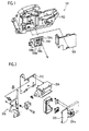
- an electric circuit is formed by a variety of connectors 104a and 104b and a parking position detection switch 104c disposed on a circuit board 104 along with various kinds of circuit components, as illustrated in Fig. 1 .
- the circuit board 104 is fixed to a body case 102, and covered and protected by a board cover 105 to be fixed to the body case 102.
- an electric component 204 such as a solenoid and a shift lock unit 206 are disposed on a bracket 210 provided separately from a circuit board 205 and the bracket 210 is mounted to a body case to mount the electric component 204 on the body case, as illustrated in Fig. 2 .
- the electric component 204 is electrically connected to the circuit board 205 via a connector 204a.
- the electric component 204 is fixed to the body case via the bracket 210. For this reason, the shift lever device has enough strength against a load to be imposed thereon.
- the shift lever device necessitates increase in the number of parts and requires a electrical connection of the connector 204a to the circuit board 205 separately from a fixation of the electric component 204 to the bracket 210, thereby resulting in low assembly workability.
- An object of the present invention is to provide a shift lever device which is capable of protecting a circuit board from a load being imposed on electric components without degrading assembly workability.
- An aspect of the present invention is a shift lever device comprising: a body case configured to pivotally support a shift lever swingably; a circuit board including a electric component disposed on a board of the circuit board; a board cover including a housing part housing the circuit board in the board cover and configured to be mounted to the body case with the circuit board being housed in the housing part; a board supporting part provided to the board cover and configured to support the circuit board in the housing part; and an electric component supporting part provided to any one of the body case and the board cover and configured to support the electric component disposed on the circuit board, wherein the circuit board is configured to be supported to the body case via the board cover.
- the circuit board is mounted to the body case via the board cover while the circuit board is housed in the housing part by the board supporting part and thus the board supporting part receives a load when a load is imposed on the electric component. For this reason, it is possible to protect the circuit board from a load being imposed on the electric component and prevent the occurrence of a bad connection or the like without taking countermeasures such as increase in the strength of the circuit board or increase in the fixation of the electric component and without degrading assembly workability. It is also possible to prevent the occurrence of a bad connection or the like due to an imposition of a load on the circuit board. It is yet possible to improve accuracy of positioning because a positioning of the electric component on the body case is accomplished through the board cover.
- the electric component supporting part may be provided to the board cover and include a support portion configured to abut on a receiver portion provided to the electric component with the circuit board being housed in the housing part.
- the electric component supporting part may be provided to the body case and include a support portion configured to abut on a receiver portion provided to the electric component with the circuit board being housed in the housing part and with the board cover being mounted to the body case.
- the receiver portion may be a through hole formed in the electric component, and the support portion may be a stepped shaft tightly disposed in the receiver portion.
- the receiver portion is a through hole formed in the electric component and the support portion is a stepped shaft tightly disposed in the receiver portion, and thus positioning of the electric component and reception of a load can be achieved through the board cover. For this reason, it is possible to improve accuracy of positioning and prevent the occurrence of a bad connection in connection parts of the electric component and the circuit board because displacement between the electric component and the circuit board is prevented when a load is imposed on the electric component.
- the receiver portion may be a through hole formed in the electric component, and the support portion may be a shaft tightly disposed in the receiver portion.
- the receiver portion is a through hole formed in the electric component and the support portion is a shaft tightly disposed in the receiver portion, and thus positioning of the electric component and imposition of a load can be achieved through the board cover. For this reason, it is possible to improve accuracy of positioning and prevent the occurrence of a bad connection in connection parts of the electric component and the circuit board because displacement between the electric component and the circuit board is prevented when a load is imposed on the electric component.
- the receiver portion may be a protrusion protruding from the electric component
- the support portion may be a cylindrical shaft having a cylindrical wall formed on a distal end of the support portion to fit the protrusion.
- the receiver portion is a protrusion protruding from the electric component and the support portion is a cylindrical shaft to fit the protrusion, and thus positioning of the electric component and imposition of a load can be achieved through the board cover. For this reason, it is possible to improve accuracy of positioning and prevent the occurrence of a bad connection in connection parts of the electric component and the circuit board because displacement between the electric component and the circuit board is prevented when a load is imposed on the electric component.
- the circuit board may have a through hole through which the electric component supporting part is disposed and having a diameter greater than a diameter of the electric component supporting part disposed through the through hole.
- a diameter of the through hole is greater than that of the electric component supporting part. Consequently, even when the electric component supporting part is slightly displaced in a direction along a board surface of the circuit board due to a load being imposed on the electric component on the circuit board, a load is not imposed on the circuit board and the circuit board can be protected due to a gap between the through hole and the electric component supporting part. For this reason, it is possible to support the electric component on the board cover with high accuracy and prevent the occurrence of a bad connection or the like between the electric component and the circuit board.
- the housing part may include a claw engaged with the electric component, with the circuit board and the electric component both being housed in the housing part in this order, and the circuit board may be configured to be supported in the housing part by an engagement of the claw with the electric component.
- the circuit board is supported in the housing part by an engagement of the claw with the electric component. Consequently, it is possible to simplify an assembly work.
- the board cover may include a peripheral wall having a fixing claw to engage with a side wall of the body case for maintaining the board cover in the body case.
- the board supporting part may include an engaging claw, a flange, and a stepped shaft, respectively protruding from an inside surface of the board cover.
- the engaging claw may include a hook-like portion to be engaged with the circuit board on a distal end of the engaging claw.
- the flange and a stepped portion of the stepped shaft may have a same protruding dimension protruding from the inside surface of the board cover.
- the circuit board may be securely mounted between the hook-like portion of the engaging claw, and the flange and the stepped portion.
- the circuit board may include a shift lock mechanism disposed thereon.
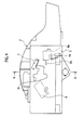
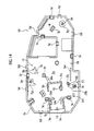
- a shift lever device 1 includes a shift lever 3 having a base end pivotally supported to a body case 2 swingably by a rotary shaft (not shown) and a shift lock mechanism (not shown) for performing a shift lock of the shift lever 3 in response to operation of a brake pedal of a vehicle (not shown).
- the body case 2 has a side wall 2a and a detent groove 2b formed in the side wall 2a.
- a position pin 3b is fit into the shift lever 3 and slides between a lock position where the position pin 3b is engaged with the detent groove 2b and an unlock position where the position pin 3b is detached from the detent groove 2b in response to operation of a knob button 3a disposed on the distal end of the shift lever 3.
- a circuit board 4 includes an electric component which electrically detects a position of the position pin 3b such as a P range position and is mounted to the body case 2 such that the circuit board 4 is interposed on the detent groove 2b.
- the circuit board 4 is covered with a board cover 5 from the outside,
- the shift lever device 1 is configured to displace the shift lever 3 between positions set within a range of swing of the shift lever 3 to shift gears to a prescribed range corresponding to each of the positions.
- the shift lock mechanism is configured to enable the shift lever 3 not to be moved from the P range position improperly for a parked vehicle by enabling the shift lever 3 to be moved only when the brake pedal (not shown) is pressed.
- the shift lock mechanism disposed in the body case 2 includes an electromagnetic solenoid 6a which is switched on in response to operation of the brake pedal (a solenoid operating portion) of the vehicle when the shift lever 3 is positioned in the P range position, a plunger 6b which is shifted by the electromagnetic solenoid 6a, and a lock member (not shown) which coordinates with the plunger 6b to shift between a lock position and an unlock position respectively for preventing and enabling movement of the position pin 3b positioned in the P range position of the detent groove 2b.
- the shift lock mechanism also includes a position switch 4a which detects the shift lever 3 being positioned in the P range position. The shift lock mechanism prevents movement of the shift lever 3 by preventing movement of the position pin 3b.
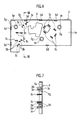
- the circuit board 4 has a mounting surface on one surface on which various electric components and circuit components are mounted, and a wiring surface on the other surface on which wirings 4d are wired as illustrated in Fig. 9 .
- the position switch (as an electric component) 4a is disposed on the mounting surface of the circuit board 4 along with the electromagnetic solenoid 6a and other circuit components. Those components have terminals electrically connected to the corresponding wirings 4d on the wiring surface through the circuit board 4.
- the position switch 4a has two through holes (receiver portions) 4b penetrating through the position switch 4a in a through-thickness direction of the circuit board 4.
- the circuit board 4 has insertion holes 4e in positions corresponding to the through holes 4b and has through holes 4f into which second stepped shaft protrusions 5e defining a board supporting part to be described are inserted.
- the circuit board 4 also has a groove 4c having the same shape as the detent groove 2b of the body case 2.
- an integrated connector 9 is disposed on the circuit board 4, and each of the electric components and the single integrated connector 9 are electrically connected to each other via the wirings 4d formed on the circuit board 4 instead of via harnesses.
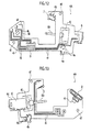
- the board cover 5 has a concave housing part 5a which is defined in the board cover 5 by a flange 5f formed on the peripheral portion of the board cover 5.
- the housing part 5a is provided with first stepped shaft protrusions (support portions) 5b which are protrudingly formed in shaft shape and are tightly inserted and disposed in the respective through holes 4b and insertion holes 4e, and the second stepped shaft protrusions 5e which are inserted into the through holes 4f.
- the first stepped shaft protrusions 5b define an electric component supporting part and the second stepped shaft protrusions 5e define the board supporting part.
- the shaft diameter in the shaft shape of the respective first stepped shaft protrusions 5b is formed thinner in two steps with steps from the base end toward the distal end of the respective first stepped shaft protrusions 5b by a stepped portion 5h.
- the shaft diameter in the shaft shape of the respective second stepped shaft protrusions 5e is also formed thinner with steps from the base end toward the distal end of the respective second stepped shaft protrusions 5e by a stepped portion 5g.
- the housing part 5a is provided with engaging claws 5c which maintain the circuit board 4 inside the housing part 5a by penetrating through through holes 4g formed in the circuit board 4 and engaging with the peripheral portion of the position switch 4a in a state where both the circuit board 4 and the position switch 4a are housed in the housing part 5a in this order.
- the engaging claws 5c define the electric component supporting part.
- the flange 5f of the board cover 5 is provided with fixing claws 5d formed so as to engage with the body case 2.
- a first electric component supporting part 11 is defined in the solenoid 6
- a second electric component supporting part 12 is defined in the position switch 4a
- a third electric component supporting part 13 is defined in a key switch 7.
- the circuit board 4 is first mounted to the board cover 5 for mounting the circuit board 4 to the body case 2.
- the stepped portions 5g of the second stepped shaft protrusions 5e position the circuit board 4 with respect to the board cover 5.
- the first stepped shaft protrusions 5b penetrating through the insertion holes 4e of the circuit board 4 to protrude from the circuit board 4 are inserted into the through holes 4b of the position switch 4a, and the engaging claws 5c penetrating through the through holes 4g are engaged with the position switch 4a.
- the engaging claws 5c and the stepped portions 5h of the first stepped shaft protrusions 5b position the position switch 4a with respect to the circuit board 4 and the board cover 5.
- the solenoid 6, and the key switch 7 and a manual mode switch 8 which cooperate with an electronic key are also mounted to the circuit board 4.
- the solenoid 6 and the manual mode switch 8 are mounted to the circuit board 4 with the engaging claws 5c penetrating through the through holes 4g
- key switch 7 is mounted to the circuit board 4 with the first stepped shaft protrusions 5b penetrating through the through holes 4b, 4b and the engaging claws 5c penetrating through the through holes 4g.
- the board cover 5 has a groove 5r having the same shape as the detent groove 2b of the body case 2, like the circuit board 4.
- the fixing claws 5d of the board cover 5 with the circuit board 4 housed therein are engaged with the body case 2 and the circuit board 4 is mounted to the body case 2 such that the circuit board 4 is interposed between the board cover 5 and the body case 2.
- the circuit board 4 is mounted to the body case 2 via the board cover 5 in a state where the circuit board 4 is housed in the housing part 5a which includes the first stepped shaft protrusions 5b, and thus the first stepped shaft protrusions 5b and/or the engaging claws 5c receive a load being imposed on the position switch 4a or the key switch 7 due to operation of the shift lever 3 or the like. Therefore, the load is not imposed on the circuit board 4 and thus it is possible to protect the circuit board 4 from the load being imposed on the position switch 4a or the key switch 7 without taking countermeasures such as increase in the strength of the fixation of the position switch 4a or the key switch 7 and without degrading assembly workability.
- the receiver portions are the through holes 4b formed in the position switch 4a or the key switch 7 and the support portions are the first stepped shaft protrusions 5b tightly disposed in the through holes 4b, and thus positioning of the position switch 4a or the key switch 7 and imposition of a load can be achieved through the board cover 5. For this reason, it is possible to improve accuracy of positioning and prevent the occurrence of a bad connection in connection parts of the position switch 4a or the key switch 7 and the circuit board 4 because displacement between the position switch 4a or the key switch 7 and the circuit board 4 is prevented when a load is imposed on the position switch 4a or the key switch 7. It is also possible to enable the support portions to receive a load being imposed on the position switch 4a or the key switch 7 without precisely setting the shape of the support portions for a direction of the load being imposed on the position switch 4a or the key switch 7.
- the circuit board 4 is maintained in the housing part 5a by engagement of the engaging claws 5c with the above-mentioned electric components such as the position switch 4a. Consequently, it is possible to simplify an assembly work.
- the terminals of the electric components penetrate from the mounting surface to the wiring surface to electrically connect to the corresponding wirings 4d in this embodiment, the terminals may be inserted and fit into corresponding sockets 4h provided on the mounting surface of the circuit board 4 for electrical connection.
- two stepped portions 5h and 5i are formed on the respective first stepped shaft protrusions 5b.
- the stepped portions 5h are for positioning of the circuit board 4 and the stepped portions 5i are for positioning of the electric components.
- the board cover 5 is engaged with the body case 2 in a state where both the circuit board 4 and the electric components are housed in the housing part 5a in this order in this embodiment, the board cover 5 may be engaged with the body case 2 in a state where both the electric components and the circuit board 4 are housed in the housing part 5a in this order. Also in this case, the same effects and advantages can be achieved.
- receiver portions may be provided to the electromagnetic solenoid 6 or the like in addition to the position switch 4a and be supported by support portions provided to the housing part 5a.
- the support portions are provided to protrude from the housing part 5a of the board cover 5 and the board cover 5 receives a load being imposed on the electric components in this embodiment, the support portions may be provided to protrude from the body case 2 and the body case 2 may receive a load being imposed on the electric components. Also in this case, the same effects and advantages can be achieved, and it is possible to improve accuracy of positioning of the electric components without degrading assembly workability because the electric components are positioned by the support portions of the body case 2.
- the integrated connector 9 is disposed on the circuit board 4 and this single integrated connector 9 and the electric components are electrically connected to each other via the wirings 4d formed on the circuit board 4 instead of harnesses. Therefore, steps of wiring harnesses for each of the electrical components and connecting the harnesses to each of the electrical components can be saved, thereby improving assembly workability.
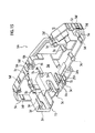
- Fig. 12 to Fig. 17 illustrate a shift lever device 1A according to a second embodiment of the present invention.
- the shift lever device 1A according to the second embodiment is different from the first embodiment mainly in the configuration of a circuit board 4A to be mounted to a board cover 5A.
- the configuration for mounting the circuit board 4A to the board cover 5A is the same as the first embodiment.
- the same constituents as those in the first embodiment are designated with the same reference numerals and duplicate description will be omitted herein.
- the circuit board 4A has one surface and the other surface both for mounting electric components and circuit components and wiring irrespective of a mounting surface and a wiring surface in the second embodiment, while the circuit board 4 has one surface as the mounting surface only for mounting electric components and circuit components, and the other surface as the wiring surface only for wiring in the first embodiment.
- the integrated connector 9 is disposed on the circuit board 4A, and this single integrated connector 9 and each of the electric components are electrically connected to each other via printed wirings 4i formed on the circuit board 4A instead of via harnesses.
- An operation force is imposed on the position switch 4a and the key switch 7 defining electric components in a direction along a board surface of the circuit board 4A.
- the first stepped shaft protrusions 5b support portions
- the operation force is imposed on the board cover 5A via the first stepped shaft protrusions 5b while the operation force is not imposed on the circuit board 4A.
- the first stepped shaft protrusions 5b position the position switch 4a and the key switch 7 with respect to the board cover 5A.
- the manual mode switch 8 defining an electric component includes three on-off switches.
- the board cover 5A is provided with a stopper protrusion 5j to be inserted into a through hole 41 formed in the circuit board 4A.
- An operation force is imposed on the manual mode switch 8 in a direction where the manual mode switch 8 is pressed to the board surface of the circuit board 4A.
- the board surface of the circuit board 4A is supported by the stopper protrusion 5j protruding from the board cover 5A. Therefore, the operation force is imposed on the board cover 5A via the stopper protrusion 5j while the operation force is not imposed on the circuit board 4A.
- the board cover 5A is provided with the fixing claws 5d on a peripheral wall 5k to engage with the side wall 2a of the body case 2 for maintaining the board cover 5A in the body case 2.
- a flanged receiver portion 2c into which the peripheral wall 5k of the board cover 5A is fit is integrally formed on the side wall 2a.
- the receiver portion 2c has engaging holes 2d with which the fixing claws 5d are engaged.
- the housing part 5a of the board cover 5A is provided with a board supporting part 10, and the first electric component supporting part 11, the second electric component supporting part 12, and the third electric component supporting part 13 as electric component supporting part s.
- the board supporting part 10 consists of the engaging claws 5c, flanges 5m, and the second stepped shaft protrusions 5e.
- the engaging claws 5c are provided to protrude from the housing part 5a and include hook-like portions to be engaged with the circuit board 4A on their distal ends.
- the flanges 5m and the stepped portions 5g of the second stepped shaft protrusions 5e have the same protruding dimension above the inside surface of the board cover 5a and the circuit board 4A is securely mounted between the hook-like portions of the engaging claws 5c, and the flanges 5m and the stepped portions 5g.
- the distal ends of the engaging claws 5c are engaged with the circuit board 4A as positioned and disposed on the flanges 5m and the stepped portions 5g to house the circuit board 4A in the housing part 5a.
- the first electric component supporting part 11 (the electric component supporting part) consists of flange walls 5n (support portions) and the engaging claws 5c.
- the flange walls 5n penetrate through an opening 4j of the circuit board 4A and surround side walls 6c (receiver portions) of the solenoid 6 on the circuit board 4A to position the solenoid 6 with respect to the board cover 5A.
- the engaging claws 5c avoid the circuit board 4A while engaging with the solenoid 6 on the circuit board 4A. Then the solenoid 6 is positioned on the circuit board 4A by the flange walls 5n and housed in the housing part 5a under engagement with the engaging claws 5c.
- the second electric component supporting part 12 (the electric component supporting part) consists of the first stepped shaft protrusions 5b (support portions) and the engaging claws 5c.
- the first stepped shaft protrusions 5b formed on a protrusion 25h penetrate through the insertion holes 4e of the circuit board 4A and are tightly inserted into the through holes 4b (receiver portions) of the position switch 4a to position the position switch 4a with respect to the board cover 5A and receive the load being imposed on the position switch 4a.
- the third electric component supporting part 13 (the electric component supporting part) consists of a flange 5s and the first stepped shaft protrusions 5b (support portions).
- the flange 5s abuts on and supports the key switch 7 on the circuit board 4A, and the first stepped shaft protrusions 5b are tightly inserted into the through holes 4b (receiver portions) of the position switch 4a, to position the position switch 4a with respect to the board cover 5A and receive the load being imposed on the position switch 4a.
- a shift lock mechanism 60 includes the solenoid 6 and a lock lever 61.
- the lock lever 61 is rotatably provided to an axis 62 protruding from the board cover 5A.
- the lock lever 61 is configured to prevent the position pin in the P range position from being moved to the other range position.
- the lock lever 61 is configured with the solenoid 6 to be movable between a lock position where the lock lever 61 is positioned on a movement locus of the position pin 3b (below the position pin 3b in Fig. 17 ) and an unlock position where the lock lever 61 is positioned out of the movement locus of the position pin 3b.
- the electric components supported by the board cover 5A can prevent the load from being applied to the circuit board 4A. Therefore, it is possible to prevent the occurrence of problems such as a bad connection and to improve both assembly accuracy and assembly workability.
- Fig. 18 to Fig. 22 illustrate a shift lever device according to a third embodiment of the present invention.
- the shift lever device according to the third embodiment is different from the first embodiment mainly in the position of the manual mode switch 8 on a circuit board 4B and in the means for fixing the position switch 4a and the key switch 7 to a board cover 5B as the electric component supporting part.
- the configuration for mounting the circuit board 4B to the board cover 5B is the same as the first embodiment.
- the same constituents as those in the first embodiment are designated with the same reference numerals and duplicate description will be omitted herein.
- the manual mode switch 8 as similar to the second embodiment, includes three on-off switches and is disposed on the circuit board 4B close to the key switch 7 which detects the shift lever 3 positioned in the parking position.
- the manual mode switch 8 In a state where the circuit board 4B is disposed with its board surface along an anteroposterior direction of the vehicle, the manual mode switch 8 is positioned in the front side of the vehicle on the circuit board 4B. Therefore, the electric components are concentrated in the vicinity of the key switch 7 on the circuit board 4B, thereby downsizing both the circuit board 4B and the board cover 5B.
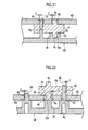
- the through hole 4b is formed in the key switch 7 as the electric component supporting part as illustrated in Fig. 21 .
- Fitting protrusions 4s, 4s protrude from both sides of the key switch 7 parallel to the through hole 4b. Terminals of the key switch 7 are electrically connected to the corresponding printed wirings formed on the circuit board 4B.
- One of the fitting protrusions 4s, 4s of the key switch 7 is inserted into one of insertion holes 4k formed in the circuit board 4B to fix the key switch 7 on the circuit board 4B.
- Two of the insertion holes 4k defining the electric component supporting part are formed in the circuit board 4B at the locations facing the through hole 4b of the key switch 7 and the one of the fitting protrusions 4s.
- the diameter of the respective insertion holes 4k is greater than that of the corresponding fitting protrusion 4s and shaft protrusion 5p to be described.
- the shaft protrusion 5p protruding into inside the housing part 5a and a cylindrical shaft 5t both defining the electric component supporting part are disposed close to each other on the board cover 5B.
- the cylindrical shaft 5t has a cylindrical wall and the other one of the fitting protrusions 4s of the key switch 7 is tightly fit into the cylindrical wall.
- the shaft protrusion 5p has no steps and has the radial portions of a constant shaft shape.
- the diameter of the shaft protrusion 5p is set such that the shaft protrusion 5p is tightly inserted into the through holes 4b when the circuit board 4B is mounted to the board cover 5B.
- the shaft protrusion 5p is inserted into one of the two insertion holes 4k.
- Clearance C is left respectively between the shaft protrusion 5p and the corresponding insertion hole 4k and between the one of the fitting protrusions 4s and the corresponding insertion hole 4k in a state where the circuit board 4B is mounted to the board cover 5B.
- the through hole 4b is also formed in the position switch 4a and the fitting protrusions 4s, 4s also protrude from both sides of the position switch 4a parallel to the through hole 4b of the position switch 4a, as illustrated in Fig. 22 .
- Terminals of the position switch 4a are electrically connected to the corresponding printed wirings formed on the circuit board 4B.
- One of the fitting protrusions 4s, 4s of the position switch 4a is inserted into one of the insertion holes 4k formed in the circuit board 4B and is tightly fit into another cylindrical shaft 5t to fix the position switch 4a on the circuit board 4B.
- Three of the insertion holes 4k are formed in the circuit board 4B at the locations facing the corresponding first stepped shaft protrusion 5b, the another cylindrical shaft 5t, and the corresponding second stepped shaft protrusion 5e.
- the diameter of the respective insertion holes 4k is greater than that of the corresponding first stepped shaft protrusion 5b, second stepped shaft protrusion 5e, and cylindrical shaft 5t.
- the board cover 5B includes the another cylindrical shaft 5t protruding therefrom inside the housing part 5a.
- the another cylindrical shaft 5t has a cylindrical wall and one of the fitting protrusions 4s of the position switch 4a inserted into the cylindrical wall.
- Clearance C is left respectively between the first stepped shaft protrusion 5b and the corresponding insertion hole 4k, between the second stepped shaft protrusion 5e and the corresponding insertion hole 4k, and between the corresponding another cylindrical shaft 5t and the corresponding insertion hole 4k in a state where the circuit board 4B is mounted to the board cover 5B.
- the circuit board 4B is positioned in the housing part 5a of the board cover 5B by the first stepped shaft protrusion 5b, the second stepped shaft protrusion 5e, the shaft protrusion 5p, and the cylindrical shafts 5t via the position switch 4a and the key switch 7.
- the position switch 4a or the key switch 7 is supported by an opening edge 5v of a cylindrical portion 5u or a bottom portion 5w of the corresponding cylindrical shaft 5t when a load imposed in a direction normal to the board surface of the circuit board 4B is imposed on the position switch 4a or the key switch 7.
- the position switch 4a or the key switch 7 is supported by the cylindrical portion 5u of the corresponding cylindrical shaft 5t, the shaft protrusion 5p, the first stepped shaft protrusion 5b and the second stepped shaft protrusion 5e when a load imposed in a direction along the board surface of the circuit board 4B is imposed on the position switch 4a or the key switch 7.
- the diameter of the respective insertion holes 4k is greater than that of the corresponding first stepped shaft protrusion 5b, second stepped shaft protrusion 5e, and cylindrical shafts 5t.
- the circuit board 4B can be protected even when the position switch 4a or the key switch 7 is slightly displaced by a load in the direction along the board surface of the circuit board 4B because the load is not imposed on the circuit board 4B due to the clearance C left respectively between the shaft protrusion 5p and the corresponding insertion hole 4k, between the fitting protrusion 4s and the corresponding insertion hole 4k, between the first stepped shaft protrusion 5b and the corresponding insertion hole 4k, between the second stepped shaft protrusion 5e and the corresponding insertion hole 4k, and between the cylindrical shafts 5t and the corresponding insertion holes 4k. Therefore, accurate support of switches such as the position switch 4a and the key switch 7 on the board cover 5B can be achieved and a bad connection between the switches and the circuit board 4B can be prevented.
Abstract
Description
- The present invention relates to a shift lever device equipped with electric components.
- Japanese Unexamined Patent Application Publication Nos.
06-080040 07-286658 - In a
shift lever device 101 described in Japanese Unexamined Patent Application Publication No.06-080040 connectors 104a and 104b and a parkingposition detection switch 104c disposed on acircuit board 104 along with various kinds of circuit components, as illustrated inFig. 1 . Thecircuit board 104 is fixed to abody case 102, and covered and protected by aboard cover 105 to be fixed to thebody case 102. - In a shift lever device described in Japanese Unexamined Patent Application Publication No.
07-286658 electric component 204 such as a solenoid and ashift lock unit 206 are disposed on abracket 210 provided separately from acircuit board 205 and thebracket 210 is mounted to a body case to mount theelectric component 204 on the body case, as illustrated inFig. 2 . Theelectric component 204 is electrically connected to thecircuit board 205 via aconnector 204a. - In the
shift lever device 101 described in Japanese Unexamined Patent Application Publication No.06-080040 circuit board 104 is damaged and electric components such as theconnectors 104a and 104b drop off due to a load, generated by manipulation of a shift lever or the like, on the parkingposition detection switch 104c being an electric component on thecircuit board 104 because thecircuit board 104 is not made strong. For this reason, countermeasures such as increase in the strength of thecircuit board 104 or increase in the strength of the fixation of the electric component need to be taken. - In the shift lever device described in Japanese Unexamined Patent Application Publication No.
07-286658 electric component 204 is fixed to the body case via thebracket 210. For this reason, the shift lever device has enough strength against a load to be imposed thereon. However, the shift lever device necessitates increase in the number of parts and requires a electrical connection of theconnector 204a to thecircuit board 205 separately from a fixation of theelectric component 204 to thebracket 210, thereby resulting in low assembly workability. - An object of the present invention is to provide a shift lever device which is capable of protecting a circuit board from a load being imposed on electric components without degrading assembly workability.
- An aspect of the present invention is a shift lever device comprising: a body case configured to pivotally support a shift lever swingably; a circuit board including a electric component disposed on a board of the circuit board; a board cover including a housing part housing the circuit board in the board cover and configured to be mounted to the body case with the circuit board being housed in the housing part; a board supporting part provided to the board cover and configured to support the circuit board in the housing part; and an electric component supporting part provided to any one of the body case and the board cover and configured to support the electric component disposed on the circuit board, wherein the circuit board is configured to be supported to the body case via the board cover.
- According to the aspect, the circuit board is mounted to the body case via the board cover while the circuit board is housed in the housing part by the board supporting part and thus the board supporting part receives a load when a load is imposed on the electric component. For this reason, it is possible to protect the circuit board from a load being imposed on the electric component and prevent the occurrence of a bad connection or the like without taking countermeasures such as increase in the strength of the circuit board or increase in the fixation of the electric component and without degrading assembly workability. It is also possible to prevent the occurrence of a bad connection or the like due to an imposition of a load on the circuit board. It is yet possible to improve accuracy of positioning because a positioning of the electric component on the body case is accomplished through the board cover.
- The electric component supporting part may be provided to the board cover and include a support portion configured to abut on a receiver portion provided to the electric component with the circuit board being housed in the housing part.
- According to this configuration, it is possible to achieve the effects and advantages similar to the above-described aspect.
- The electric component supporting part may be provided to the body case and include a support portion configured to abut on a receiver portion provided to the electric component with the circuit board being housed in the housing part and with the board cover being mounted to the body case.
- According to this configuration, it is possible to achieve the effects and advantages similar to the above-described aspect.
- The receiver portion may be a through hole formed in the electric component, and the support portion may be a stepped shaft tightly disposed in the receiver portion.
- According to this configuration, the receiver portion is a through hole formed in the electric component and the support portion is a stepped shaft tightly disposed in the receiver portion, and thus positioning of the electric component and reception of a load can be achieved through the board cover. For this reason, it is possible to improve accuracy of positioning and prevent the occurrence of a bad connection in connection parts of the electric component and the circuit board because displacement between the electric component and the circuit board is prevented when a load is imposed on the electric component.
- The receiver portion may be a through hole formed in the electric component, and the support portion may be a shaft tightly disposed in the receiver portion.
- According to this configuration, the receiver portion is a through hole formed in the electric component and the support portion is a shaft tightly disposed in the receiver portion, and thus positioning of the electric component and imposition of a load can be achieved through the board cover. For this reason, it is possible to improve accuracy of positioning and prevent the occurrence of a bad connection in connection parts of the electric component and the circuit board because displacement between the electric component and the circuit board is prevented when a load is imposed on the electric component.
- The receiver portion may be a protrusion protruding from the electric component, and the support portion may be a cylindrical shaft having a cylindrical wall formed on a distal end of the support portion to fit the protrusion.
- According to this configuration, the receiver portion is a protrusion protruding from the electric component and the support portion is a cylindrical shaft to fit the protrusion, and thus positioning of the electric component and imposition of a load can be achieved through the board cover. For this reason, it is possible to improve accuracy of positioning and prevent the occurrence of a bad connection in connection parts of the electric component and the circuit board because displacement between the electric component and the circuit board is prevented when a load is imposed on the electric component.
- The circuit board may have a through hole through which the electric component supporting part is disposed and having a diameter greater than a diameter of the electric component supporting part disposed through the through hole.
- According to this configuration, a diameter of the through hole is greater than that of the electric component supporting part. Consequently, even when the electric component supporting part is slightly displaced in a direction along a board surface of the circuit board due to a load being imposed on the electric component on the circuit board, a load is not imposed on the circuit board and the circuit board can be protected due to a gap between the through hole and the electric component supporting part. For this reason, it is possible to support the electric component on the board cover with high accuracy and prevent the occurrence of a bad connection or the like between the electric component and the circuit board.
- The housing part may include a claw engaged with the electric component, with the circuit board and the electric component both being housed in the housing part in this order, and the circuit board may be configured to be supported in the housing part by an engagement of the claw with the electric component.
- According to this configuration, the circuit board is supported in the housing part by an engagement of the claw with the electric component. Consequently, it is possible to simplify an assembly work.
- The board cover may include a peripheral wall having a fixing claw to engage with a side wall of the body case for maintaining the board cover in the body case.
- The board supporting part may include an engaging claw, a flange, and a stepped shaft, respectively protruding from an inside surface of the board cover. The engaging claw may include a hook-like portion to be engaged with the circuit board on a distal end of the engaging claw. The flange and a stepped portion of the stepped shaft may have a same protruding dimension protruding from the inside surface of the board cover. The circuit board may be securely mounted between the hook-like portion of the engaging claw, and the flange and the stepped portion.
- The circuit board may include a shift lock mechanism disposed thereon.
-
-
Fig. 1 is an exploded perspective view of a first related shift lever device. -
Fig. 2 is an exploded perspective view of a second related shift lever device. -
Fig. 3 is an exploded perspective view of a shift lever device according to a first embodiment of the present invention. -
Fig. 4 is a side view of a body case according to the first embodiment of the present invention. -
Fig. 5 is a cross-sectional view taken along the V-V line inFig. 4 . -
Fig. 6 is a plan view of a board cover according to the first embodiment of the present invention. -
Fig. 7 is a cross-sectional view taken along the VII-VII line inFig. 6 . -
Fig. 8 is a plan view illustrating a mounting surface of a circuit board according to the first embodiment of the present invention. -
Fig. 9 is a plan view illustrating a wiring surface of the circuit board according to the first embodiment of the present invention. -
FIG. 10 is an enlarged view of the essential parts illustrating a state where the circuit board is mounted to the board cover according to the first embodiment of the present invention. -
FIG. 11 is an enlarged view of the essential parts illustrating a state where a circuit board is mounted to a board cover according to a modification of the first embodiment of the present invention. -
Fig. 12 is a plan view illustrating one surface of a circuit board according to a second embodiment of the present invention. -
Fig. 13 is a plan view illustrating the other surface of the circuit board according to the second embodiment of the present invention. -
Fig. 14 is a plan view of a board cover according to the second embodiment of the present invention. -
Fig. 15 is a perspective view illustrating a housing part side of the board cover according to the second embodiment of the present invention. -
Fig. 16 is an exploded perspective view of a shift lever device according to the second embodiment of the present invention. -
FIG. 17 is a plan view illustrating a state where the circuit board is mounted to the board cover according to the second embodiment of the present invention. -
FIG. 18 is a perspective view illustrating a state where a circuit board is mounted to a board cover according to a third embodiment of the present invention. -
Fig. 19 is a perspective view illustrating a housing part side of the board cover according to the third embodiment of the present invention. -
FIG. 20 is a plan view illustrating a state where the circuit board is mounted to the board cover according to the third embodiment of the present invention. -
Fig. 21 is a cross-sectional view taken along the XXI-XXI line inFig. 20 . -
Fig. 22 is a cross-sectional view taken along the XXII-XXII line inFig. 20 . - Hereinafter, embodiments of the present invention will be described in detail with reference to the drawings.
- As illustrated in
Fig. 3 to Fig. 10 , a shift lever device 1 includes a shift lever 3 having a base end pivotally supported to abody case 2 swingably by a rotary shaft (not shown) and a shift lock mechanism (not shown) for performing a shift lock of the shift lever 3 in response to operation of a brake pedal of a vehicle (not shown). Thebody case 2 has aside wall 2a and a detent groove 2b formed in theside wall 2a. Aposition pin 3b is fit into the shift lever 3 and slides between a lock position where theposition pin 3b is engaged with the detent groove 2b and an unlock position where theposition pin 3b is detached from the detent groove 2b in response to operation of a knob button 3a disposed on the distal end of the shift lever 3. Acircuit board 4 includes an electric component which electrically detects a position of theposition pin 3b such as a P range position and is mounted to thebody case 2 such that thecircuit board 4 is interposed on the detent groove 2b. Thecircuit board 4 is covered with aboard cover 5 from the outside, - The shift lever device 1 is configured to displace the shift lever 3 between positions set within a range of swing of the shift lever 3 to shift gears to a prescribed range corresponding to each of the positions. The shift lock mechanism is configured to enable the shift lever 3 not to be moved from the P range position improperly for a parked vehicle by enabling the shift lever 3 to be moved only when the brake pedal (not shown) is pressed.
- The shift lock mechanism disposed in the
body case 2 includes anelectromagnetic solenoid 6a which is switched on in response to operation of the brake pedal (a solenoid operating portion) of the vehicle when the shift lever 3 is positioned in the P range position, aplunger 6b which is shifted by theelectromagnetic solenoid 6a, and a lock member (not shown) which coordinates with theplunger 6b to shift between a lock position and an unlock position respectively for preventing and enabling movement of theposition pin 3b positioned in the P range position of the detent groove 2b. The shift lock mechanism also includes aposition switch 4a which detects the shift lever 3 being positioned in the P range position. The shift lock mechanism prevents movement of the shift lever 3 by preventing movement of theposition pin 3b. - The
circuit board 4 has a mounting surface on one surface on which various electric components and circuit components are mounted, and a wiring surface on the other surface on whichwirings 4d are wired as illustrated inFig. 9 . The position switch (as an electric component) 4a is disposed on the mounting surface of thecircuit board 4 along with theelectromagnetic solenoid 6a and other circuit components. Those components have terminals electrically connected to the correspondingwirings 4d on the wiring surface through thecircuit board 4. Theposition switch 4a has two through holes (receiver portions) 4b penetrating through theposition switch 4a in a through-thickness direction of thecircuit board 4. Thecircuit board 4 hasinsertion holes 4e in positions corresponding to the throughholes 4b and has throughholes 4f into which second steppedshaft protrusions 5e defining a board supporting part to be described are inserted. Thecircuit board 4 also has agroove 4c having the same shape as the detent groove 2b of thebody case 2. - In the present embodiment, an integrated connector 9 is disposed on the
circuit board 4, and each of the electric components and the single integrated connector 9 are electrically connected to each other via thewirings 4d formed on thecircuit board 4 instead of via harnesses. - The
board cover 5 has aconcave housing part 5a which is defined in theboard cover 5 by aflange 5f formed on the peripheral portion of theboard cover 5. Thehousing part 5a is provided with first stepped shaft protrusions (support portions) 5b which are protrudingly formed in shaft shape and are tightly inserted and disposed in the respective throughholes 4b andinsertion holes 4e, and the second steppedshaft protrusions 5e which are inserted into the throughholes 4f. The first steppedshaft protrusions 5b define an electric component supporting part and the second steppedshaft protrusions 5e define the board supporting part. The shaft diameter in the shaft shape of the respective first steppedshaft protrusions 5b is formed thinner in two steps with steps from the base end toward the distal end of the respective first steppedshaft protrusions 5b by a steppedportion 5h. The shaft diameter in the shaft shape of the respective second steppedshaft protrusions 5e is also formed thinner with steps from the base end toward the distal end of the respective second steppedshaft protrusions 5e by a steppedportion 5g. Thehousing part 5a is provided with engagingclaws 5c which maintain thecircuit board 4 inside thehousing part 5a by penetrating through throughholes 4g formed in thecircuit board 4 and engaging with the peripheral portion of theposition switch 4a in a state where both thecircuit board 4 and theposition switch 4a are housed in thehousing part 5a in this order. The engagingclaws 5c define the electric component supporting part. Theflange 5f of theboard cover 5 is provided with fixingclaws 5d formed so as to engage with thebody case 2. A first electriccomponent supporting part 11 is defined in thesolenoid 6, a second electriccomponent supporting part 12 is defined in theposition switch 4a, and a third electriccomponent supporting part 13 is defined in akey switch 7. - With the above arrangement, the
circuit board 4 is first mounted to theboard cover 5 for mounting thecircuit board 4 to thebody case 2. At this time, the steppedportions 5g of the second steppedshaft protrusions 5e position thecircuit board 4 with respect to theboard cover 5. Then the first steppedshaft protrusions 5b penetrating through theinsertion holes 4e of thecircuit board 4 to protrude from thecircuit board 4 are inserted into the throughholes 4b of theposition switch 4a, and the engagingclaws 5c penetrating through the throughholes 4g are engaged with theposition switch 4a. By these operations, the engagingclaws 5c and the steppedportions 5h of the first steppedshaft protrusions 5b position theposition switch 4a with respect to thecircuit board 4 and theboard cover 5. Similarly, as electric components, thesolenoid 6, and thekey switch 7 and amanual mode switch 8 which cooperate with an electronic key are also mounted to thecircuit board 4. Thesolenoid 6 and themanual mode switch 8 are mounted to thecircuit board 4 with the engagingclaws 5c penetrating through the throughholes 4g, andkey switch 7 is mounted to thecircuit board 4 with the first steppedshaft protrusions 5b penetrating through the throughholes claws 5c penetrating through the throughholes 4g. Theboard cover 5 has agroove 5r having the same shape as the detent groove 2b of thebody case 2, like thecircuit board 4. - Next, the fixing
claws 5d of theboard cover 5 with thecircuit board 4 housed therein are engaged with thebody case 2 and thecircuit board 4 is mounted to thebody case 2 such that thecircuit board 4 is interposed between theboard cover 5 and thebody case 2. - According to this embodiment, the
circuit board 4 is mounted to thebody case 2 via theboard cover 5 in a state where thecircuit board 4 is housed in thehousing part 5a which includes the first steppedshaft protrusions 5b, and thus the first steppedshaft protrusions 5b and/or the engagingclaws 5c receive a load being imposed on theposition switch 4a or thekey switch 7 due to operation of the shift lever 3 or the like. Therefore, the load is not imposed on thecircuit board 4 and thus it is possible to protect thecircuit board 4 from the load being imposed on theposition switch 4a or thekey switch 7 without taking countermeasures such as increase in the strength of the fixation of theposition switch 4a or thekey switch 7 and without degrading assembly workability. - The receiver portions are the through
holes 4b formed in theposition switch 4a or thekey switch 7 and the support portions are the first steppedshaft protrusions 5b tightly disposed in the throughholes 4b, and thus positioning of theposition switch 4a or thekey switch 7 and imposition of a load can be achieved through theboard cover 5. For this reason, it is possible to improve accuracy of positioning and prevent the occurrence of a bad connection in connection parts of theposition switch 4a or thekey switch 7 and thecircuit board 4 because displacement between theposition switch 4a or thekey switch 7 and thecircuit board 4 is prevented when a load is imposed on theposition switch 4a or thekey switch 7. It is also possible to enable the support portions to receive a load being imposed on theposition switch 4a or thekey switch 7 without precisely setting the shape of the support portions for a direction of the load being imposed on theposition switch 4a or thekey switch 7. - The
circuit board 4 is maintained in thehousing part 5a by engagement of the engagingclaws 5c with the above-mentioned electric components such as theposition switch 4a. Consequently, it is possible to simplify an assembly work. - It is possible to perform positioning between the electric components (such as switches) mounted to the
circuit board 4 and the shift lever 3 by fitting the second steppedshaft protrusions 5e into fitting holes (not shown) formed in thebody case 2 after positioning thecircuit board 4 with the steppedportions 5g of the second steppedshaft protrusions 5e formed on theboard cover 5. The height of the steppedportion 5g of the respective second steppedshaft protrusions 5e above theboard cover 5 is the same as that of the steppedportion 5h of the respective first steppedshaft protrusions 5b. These steppedportions circuit board 4 with respect to theboard cover 5. - Although the terminals of the electric components penetrate from the mounting surface to the wiring surface to electrically connect to the corresponding
wirings 4d in this embodiment, the terminals may be inserted and fit into correspondingsockets 4h provided on the mounting surface of thecircuit board 4 for electrical connection. In this case, two steppedportions 5h and 5i are formed on the respective first steppedshaft protrusions 5b. The steppedportions 5h are for positioning of thecircuit board 4 and the stepped portions 5i are for positioning of the electric components. - Although the
board cover 5 is engaged with thebody case 2 in a state where both thecircuit board 4 and the electric components are housed in thehousing part 5a in this order in this embodiment, theboard cover 5 may be engaged with thebody case 2 in a state where both the electric components and thecircuit board 4 are housed in thehousing part 5a in this order. Also in this case, the same effects and advantages can be achieved. - Although the through
holes 4b are provided to theposition switch 4a as an electric component and are supported by the first steppedshaft protrusions 5b of thehousing part 5a in this embodiment, receiver portions may be provided to theelectromagnetic solenoid 6 or the like in addition to theposition switch 4a and be supported by support portions provided to thehousing part 5a. - Although the support portions are provided to protrude from the
housing part 5a of theboard cover 5 and theboard cover 5 receives a load being imposed on the electric components in this embodiment, the support portions may be provided to protrude from thebody case 2 and thebody case 2 may receive a load being imposed on the electric components. Also in this case, the same effects and advantages can be achieved, and it is possible to improve accuracy of positioning of the electric components without degrading assembly workability because the electric components are positioned by the support portions of thebody case 2. - The integrated connector 9 is disposed on the
circuit board 4 and this single integrated connector 9 and the electric components are electrically connected to each other via thewirings 4d formed on thecircuit board 4 instead of harnesses. Therefore, steps of wiring harnesses for each of the electrical components and connecting the harnesses to each of the electrical components can be saved, thereby improving assembly workability. -
Fig. 12 to Fig. 17 illustrate ashift lever device 1A according to a second embodiment of the present invention. Theshift lever device 1A according to the second embodiment is different from the first embodiment mainly in the configuration of acircuit board 4A to be mounted to aboard cover 5A. The configuration for mounting thecircuit board 4A to theboard cover 5A is the same as the first embodiment. In the second embodiment, the same constituents as those in the first embodiment are designated with the same reference numerals and duplicate description will be omitted herein. - The
circuit board 4A has one surface and the other surface both for mounting electric components and circuit components and wiring irrespective of a mounting surface and a wiring surface in the second embodiment, while thecircuit board 4 has one surface as the mounting surface only for mounting electric components and circuit components, and the other surface as the wiring surface only for wiring in the first embodiment. - In this embodiment, the integrated connector 9 is disposed on the
circuit board 4A, and this single integrated connector 9 and each of the electric components are electrically connected to each other via printedwirings 4i formed on thecircuit board 4A instead of via harnesses. - An operation force is imposed on the
position switch 4a and thekey switch 7 defining electric components in a direction along a board surface of thecircuit board 4A. However, the first steppedshaft protrusions 5b (support portions) are inserted into the throughholes 4b to support the throughholes 4b. Therefore, the operation force is imposed on theboard cover 5A via the first steppedshaft protrusions 5b while the operation force is not imposed on thecircuit board 4A. The first steppedshaft protrusions 5b position theposition switch 4a and thekey switch 7 with respect to theboard cover 5A. - The
manual mode switch 8 defining an electric component includes three on-off switches. Theboard cover 5A is provided with astopper protrusion 5j to be inserted into a throughhole 41 formed in thecircuit board 4A. An operation force is imposed on themanual mode switch 8 in a direction where themanual mode switch 8 is pressed to the board surface of thecircuit board 4A. However, the board surface of thecircuit board 4A is supported by thestopper protrusion 5j protruding from theboard cover 5A. Therefore, the operation force is imposed on theboard cover 5A via thestopper protrusion 5j while the operation force is not imposed on thecircuit board 4A. - The
board cover 5A is provided with the fixingclaws 5d on aperipheral wall 5k to engage with theside wall 2a of thebody case 2 for maintaining theboard cover 5A in thebody case 2. Aflanged receiver portion 2c into which theperipheral wall 5k of theboard cover 5A is fit is integrally formed on theside wall 2a. Thereceiver portion 2c has engagingholes 2d with which the fixingclaws 5d are engaged. Thehousing part 5a of theboard cover 5A is provided with aboard supporting part 10, and the first electriccomponent supporting part 11, the second electriccomponent supporting part 12, and the third electriccomponent supporting part 13 as electric component supporting part s. - The
board supporting part 10 consists of the engagingclaws 5c,flanges 5m, and the second steppedshaft protrusions 5e. The engagingclaws 5c are provided to protrude from thehousing part 5a and include hook-like portions to be engaged with thecircuit board 4A on their distal ends. Theflanges 5m and the steppedportions 5g of the second steppedshaft protrusions 5e have the same protruding dimension above the inside surface of theboard cover 5a and thecircuit board 4A is securely mounted between the hook-like portions of the engagingclaws 5c, and theflanges 5m and the steppedportions 5g. The distal ends of the engagingclaws 5c are engaged with thecircuit board 4A as positioned and disposed on theflanges 5m and the steppedportions 5g to house thecircuit board 4A in thehousing part 5a. - The first electric component supporting part 11 (the electric component supporting part) consists of
flange walls 5n (support portions) and the engagingclaws 5c. Theflange walls 5n penetrate through anopening 4j of thecircuit board 4A and surroundside walls 6c (receiver portions) of thesolenoid 6 on thecircuit board 4A to position thesolenoid 6 with respect to theboard cover 5A. The engagingclaws 5c avoid thecircuit board 4A while engaging with thesolenoid 6 on thecircuit board 4A. Then thesolenoid 6 is positioned on thecircuit board 4A by theflange walls 5n and housed in thehousing part 5a under engagement with the engagingclaws 5c. - The second electric component supporting part 12 (the electric component supporting part) consists of the first stepped
shaft protrusions 5b (support portions) and the engagingclaws 5c. The first steppedshaft protrusions 5b formed on aprotrusion 25h penetrate through theinsertion holes 4e of thecircuit board 4A and are tightly inserted into the throughholes 4b (receiver portions) of theposition switch 4a to position theposition switch 4a with respect to theboard cover 5A and receive the load being imposed on theposition switch 4a. - The third electric component supporting part 13 (the electric component supporting part) consists of a flange 5s and the first stepped
shaft protrusions 5b (support portions). The flange 5s abuts on and supports thekey switch 7 on thecircuit board 4A, and the first steppedshaft protrusions 5b are tightly inserted into the throughholes 4b (receiver portions) of theposition switch 4a, to position theposition switch 4a with respect to theboard cover 5A and receive the load being imposed on theposition switch 4a. - A
shift lock mechanism 60 includes thesolenoid 6 and alock lever 61. Thelock lever 61 is rotatably provided to anaxis 62 protruding from theboard cover 5A. Thelock lever 61 is configured to prevent the position pin in the P range position from being moved to the other range position. Thelock lever 61 is configured with thesolenoid 6 to be movable between a lock position where thelock lever 61 is positioned on a movement locus of theposition pin 3b (below theposition pin 3b inFig. 17 ) and an unlock position where thelock lever 61 is positioned out of the movement locus of theposition pin 3b. - With the above-mentioned configurations where the integrated connector 9 is disposed on the
circuit board 4A and this single integrated connector 9 and the electric components are electrically connected to each other via printedwirings 4i formed on thecircuit board 4A instead of via harnesses, steps of wiring harnesses for each of the electrical components and connecting the harnesses to each of the electrical components can be saved, thereby improving assembly workability. - With the above-mentioned configurations, even in the configuration where the electric components are connected to the
circuit board 4A by soldering or the like, the electric components supported by theboard cover 5A can prevent the load from being applied to thecircuit board 4A. Therefore, it is possible to prevent the occurrence of problems such as a bad connection and to improve both assembly accuracy and assembly workability. -
Fig. 18 to Fig. 22 illustrate a shift lever device according to a third embodiment of the present invention. The shift lever device according to the third embodiment is different from the first embodiment mainly in the position of themanual mode switch 8 on acircuit board 4B and in the means for fixing theposition switch 4a and thekey switch 7 to aboard cover 5B as the electric component supporting part. The configuration for mounting thecircuit board 4B to theboard cover 5B is the same as the first embodiment. In the third embodiment, the same constituents as those in the first embodiment are designated with the same reference numerals and duplicate description will be omitted herein. - The
manual mode switch 8, as similar to the second embodiment, includes three on-off switches and is disposed on thecircuit board 4B close to thekey switch 7 which detects the shift lever 3 positioned in the parking position. In a state where thecircuit board 4B is disposed with its board surface along an anteroposterior direction of the vehicle, themanual mode switch 8 is positioned in the front side of the vehicle on thecircuit board 4B. Therefore, the electric components are concentrated in the vicinity of thekey switch 7 on thecircuit board 4B, thereby downsizing both thecircuit board 4B and theboard cover 5B. - The through
hole 4b is formed in thekey switch 7 as the electric component supporting part as illustrated inFig. 21 . Fittingprotrusions key switch 7 parallel to the throughhole 4b. Terminals of thekey switch 7 are electrically connected to the corresponding printed wirings formed on thecircuit board 4B. One of thefitting protrusions key switch 7 is inserted into one ofinsertion holes 4k formed in thecircuit board 4B to fix thekey switch 7 on thecircuit board 4B. - Two of the insertion holes 4k defining the electric component supporting part are formed in the
circuit board 4B at the locations facing the throughhole 4b of thekey switch 7 and the one of thefitting protrusions 4s. The diameter of therespective insertion holes 4k is greater than that of the correspondingfitting protrusion 4s andshaft protrusion 5p to be described. - The
shaft protrusion 5p protruding into inside thehousing part 5a and acylindrical shaft 5t both defining the electric component supporting part are disposed close to each other on theboard cover 5B. Thecylindrical shaft 5t has a cylindrical wall and the other one of thefitting protrusions 4s of thekey switch 7 is tightly fit into the cylindrical wall. Theshaft protrusion 5p has no steps and has the radial portions of a constant shaft shape. The diameter of theshaft protrusion 5p is set such that theshaft protrusion 5p is tightly inserted into the throughholes 4b when thecircuit board 4B is mounted to theboard cover 5B. Theshaft protrusion 5p is inserted into one of the twoinsertion holes 4k. - Clearance C is left respectively between the
shaft protrusion 5p and thecorresponding insertion hole 4k and between the one of thefitting protrusions 4s and thecorresponding insertion hole 4k in a state where thecircuit board 4B is mounted to theboard cover 5B. - The through
hole 4b is also formed in theposition switch 4a and thefitting protrusions position switch 4a parallel to the throughhole 4b of theposition switch 4a, as illustrated inFig. 22 . Terminals of theposition switch 4a are electrically connected to the corresponding printed wirings formed on thecircuit board 4B. One of thefitting protrusions position switch 4a is inserted into one of theinsertion holes 4k formed in thecircuit board 4B and is tightly fit into anothercylindrical shaft 5t to fix theposition switch 4a on thecircuit board 4B. - Three of the insertion holes 4k are formed in the
circuit board 4B at the locations facing the corresponding first steppedshaft protrusion 5b, the anothercylindrical shaft 5t, and the corresponding second steppedshaft protrusion 5e. The diameter of therespective insertion holes 4k is greater than that of the corresponding first steppedshaft protrusion 5b, second steppedshaft protrusion 5e, andcylindrical shaft 5t. - The
board cover 5B includes the anothercylindrical shaft 5t protruding therefrom inside thehousing part 5a. The anothercylindrical shaft 5t has a cylindrical wall and one of thefitting protrusions 4s of theposition switch 4a inserted into the cylindrical wall. - Clearance C is left respectively between the first stepped
shaft protrusion 5b and thecorresponding insertion hole 4k, between the second steppedshaft protrusion 5e and thecorresponding insertion hole 4k, and between the corresponding anothercylindrical shaft 5t and thecorresponding insertion hole 4k in a state where thecircuit board 4B is mounted to theboard cover 5B. - With the above-mentioned configurations, the
circuit board 4B is positioned in thehousing part 5a of theboard cover 5B by the first steppedshaft protrusion 5b, the second steppedshaft protrusion 5e, theshaft protrusion 5p, and thecylindrical shafts 5t via theposition switch 4a and thekey switch 7. - The
position switch 4a or thekey switch 7 is supported by anopening edge 5v of acylindrical portion 5u or abottom portion 5w of the correspondingcylindrical shaft 5t when a load imposed in a direction normal to the board surface of thecircuit board 4B is imposed on theposition switch 4a or thekey switch 7. Theposition switch 4a or thekey switch 7 is supported by thecylindrical portion 5u of the correspondingcylindrical shaft 5t, theshaft protrusion 5p, the first steppedshaft protrusion 5b and the second steppedshaft protrusion 5e when a load imposed in a direction along the board surface of thecircuit board 4B is imposed on theposition switch 4a or thekey switch 7. As mentioned above, the diameter of therespective insertion holes 4k is greater than that of the corresponding first steppedshaft protrusion 5b, second steppedshaft protrusion 5e, andcylindrical shafts 5t. For this reason, thecircuit board 4B can be protected even when theposition switch 4a or thekey switch 7 is slightly displaced by a load in the direction along the board surface of thecircuit board 4B because the load is not imposed on thecircuit board 4B due to the clearance C left respectively between theshaft protrusion 5p and thecorresponding insertion hole 4k, between thefitting protrusion 4s and thecorresponding insertion hole 4k, between the first steppedshaft protrusion 5b and thecorresponding insertion hole 4k, between the second steppedshaft protrusion 5e and thecorresponding insertion hole 4k, and between thecylindrical shafts 5t and thecorresponding insertion holes 4k. Therefore, accurate support of switches such as theposition switch 4a and thekey switch 7 on theboard cover 5B can be achieved and a bad connection between the switches and thecircuit board 4B can be prevented. - Although the shift lever device of the present invention has been described based on the first to third embodiments as examples, it is to be noted that the present invention is not limited only to these embodiments and various other embodiments may also be applicable.
Claims (11)
- A shift lever device comprisinga body case configured to pivotally support a shift lever swingably;a circuit board including a electric component disposed on a board of the circuit board;a board cover including a housing part housing the circuit board in the board cover and configured to be mounted to the body case with the circuit board being housed in the housing part;a board supporting part provided to the board cover and configured to support the circuit board in the housing part; andan electric component supporting part provided to any one of the body case and the board cover and configured to support the electric component disposed on the circuit board,wherein the circuit board is configured to be supported to the body case via the board cover.
- The shift lever device according to claim 1, wherein the electric component supporting part is provided to the board cover and includes a support portion configured to abut on a receiver portion provided to the electric component with the circuit board being housed in the housing part.
- The shift lever device according to claim 1, wherein the electric component supporting part is provided to the body case and includes a support portion configured to abut on a receiver portion provided to the electric component with the circuit board being housed in the housing part and with the board cover being mounted to the body case.
- The shift lever device according to claim 2 or 3, wherein
the receiver portion is a through hole formed in the electric component, and
the support portion is a stepped shaft tightly disposed in the receiver portion. - The shift lever device according to claim 2 or 3, wherein
the receiver portion is a through hole formed in the electric component, and
the support portion is a shaft tightly disposed in the receiver portion. - The shift lever device according to claim 2 or 3, wherein
the receiver portion is a protrusion protruding from the electric component, and
the support portion is a cylindrical shaft having a cylindrical wall formed on a distal end of the support portion to fit the protrusion. - The shift lever device according to any one of claims 1 to 4, wherein the circuit board has a through hole through which the electric component supporting part is disposed and having a diameter greater than a diameter of the electric component supporting part disposed through the through hole.
- The shift lever device according to any one of claims 1 to 7, wherein
the housing part includes a claw engaged with the electric component, with the circuit board and the electric component both being housed in the housing part in this order, and
the circuit board is configured to be supported in the housing part by an engagement of the claw with the electric component. - The shift lever device according to any one of claims 1 to 8, wherein the board cover includes a peripheral wall having a fixing claw to engage with a side wall of the body case for maintaining the board cover in the body case.
- The shift lever device according to any one of claims 1 to 7 and 9, wherein
the board supporting part includes an engaging claw, a flange, and a stepped shaft, respectively protruding from an inside surface of the board cover,
the engaging claw includes a hook-like portion to be engaged with the circuit board on a distal end of the engaging claw,
the flange and a stepped portion of the stepped shaft have a same protruding dimension protruding from the inside surface of the board cover, and
the circuit board is securely mounted between the hook-like portion of the engaging claw, and the flange and the stepped portion. - The shift lever device according to any one of claims 1 to 10, wherein the circuit board includes a shift lock mechanism disposed thereon.
Applications Claiming Priority (2)
| Application Number | Priority Date | Filing Date | Title |
|---|---|---|---|
| JP2010078033 | 2010-03-30 | ||
| JP2010265103A JP2011225200A (en) | 2010-03-30 | 2010-11-29 | Shift lever device |
Publications (2)
| Publication Number | Publication Date |
|---|---|
| EP2371606A2 true EP2371606A2 (en) | 2011-10-05 |
| EP2371606A3 EP2371606A3 (en) | 2013-12-25 |
Family
ID=44243323
Family Applications (1)
| Application Number | Title | Priority Date | Filing Date |
|---|---|---|---|
| EP11160019.3A Withdrawn EP2371606A3 (en) | 2010-03-30 | 2011-03-28 | Shift lever device |
Country Status (4)
| Country | Link |
|---|---|
| US (1) | US8616081B2 (en) |
| EP (1) | EP2371606A3 (en) |
| JP (1) | JP2011225200A (en) |
| CN (1) | CN102205794A (en) |
Cited By (1)
| Publication number | Priority date | Publication date | Assignee | Title |
|---|---|---|---|---|
| DE102014116990B4 (en) | 2014-11-20 | 2023-03-02 | Hyundai Motor Company | Motor vehicle transmission with shift lever and transmission sensor module |
Families Citing this family (6)
| Publication number | Priority date | Publication date | Assignee | Title |
|---|---|---|---|---|
| JP6026800B2 (en) * | 2012-07-11 | 2016-11-16 | 株式会社東海理化電機製作所 | Shift device |
| JP5872445B2 (en) * | 2012-12-12 | 2016-03-01 | 株式会社東海理化電機製作所 | Shift device |
| KR101558766B1 (en) | 2014-05-08 | 2015-10-12 | 현대자동차주식회사 | Gear-shift lever module |
| DE102016119842B3 (en) * | 2016-10-18 | 2018-02-22 | Preh Gmbh | Mode selector for a vehicle transmission with slide mechanism |
| JP6858608B2 (en) * | 2017-03-21 | 2021-04-14 | 株式会社アツミテック | Speed change control device |
| JP2018167651A (en) * | 2017-03-29 | 2018-11-01 | 富士機工株式会社 | Shift lever device |
Citations (3)
| Publication number | Priority date | Publication date | Assignee | Title |
|---|---|---|---|---|
| JPH0680040A (en) | 1992-07-15 | 1994-03-22 | Kojima Press Co Ltd | Shift lever device |
| JPH07286668A (en) | 1994-04-15 | 1995-10-31 | Shimizu Corp | Sealing gasket joint structure for four-point supported rectangular glass plate |
| JPH07286658A (en) | 1994-04-18 | 1995-10-31 | Tokai Rika Co Ltd | Shift lock unit |
Family Cites Families (24)
| Publication number | Priority date | Publication date | Assignee | Title |
|---|---|---|---|---|
| US4228879A (en) * | 1978-09-28 | 1980-10-21 | Deere & Company | Tractor transmission shift control |
| EP0575658B1 (en) * | 1992-06-30 | 1998-10-28 | Aisin Aw Co., Ltd. | Shift system having a manual speed selecting mechanism for a vehicular automatic transmission |
| JPH0680038A (en) * | 1992-07-15 | 1994-03-22 | Kojima Press Co Ltd | Shift lever device |
| JP2519639B2 (en) * | 1992-09-01 | 1996-07-31 | 小島プレス工業株式会社 | Shift lever device |
| US5388476A (en) * | 1993-06-15 | 1995-02-14 | Agco Corporation | Gearshift mechanism |
| JP2963342B2 (en) * | 1994-07-15 | 1999-10-18 | 小島プレス工業株式会社 | Shift lever device and method of assembling the same |
| JP2000251556A (en) * | 1999-02-25 | 2000-09-14 | Kayaba Ind Co Ltd | Controller |
| JP3799900B2 (en) * | 1999-10-07 | 2006-07-19 | 三菱自動車工業株式会社 | Shift switch device for vehicle |
| US6852065B2 (en) * | 2000-09-19 | 2005-02-08 | Kabushiki Kaisha Tokai-Rika-Denki-Seisakusho | Lock mechanism, shift lever device, and shift lock unit |
| JP2002144905A (en) * | 2000-11-16 | 2002-05-22 | Niles Parts Co Ltd | Shift operating device for automatic transmission |
| EP1314912B1 (en) * | 2001-11-22 | 2006-09-27 | Kabushiki Kaisha Tokai Rika Denki Seisakusho | Shift device |
| JP3996380B2 (en) * | 2001-11-27 | 2007-10-24 | 株式会社東海理化電機製作所 | Shift lock device |
| JP4205372B2 (en) * | 2002-06-28 | 2009-01-07 | 富士重工業株式会社 | Automatic transmission selection system |
| US7621198B2 (en) * | 2003-08-22 | 2009-11-24 | Kabushiki Kaisha Tokai-Rika-Denki-Seisakusho | Shift lever device |
| JP2005119517A (en) * | 2003-10-17 | 2005-05-12 | Fuji Kiko Co Ltd | Backlash suppressing bearing structure for rotary shaft part |
| DE10361209B8 (en) * | 2003-12-24 | 2005-09-29 | Teleflex Automotive Germany Gmbh | Device for switching a mechanical switching means |
| DE102004006150B3 (en) * | 2004-02-07 | 2005-09-15 | Teleflex Automotive Germany Gmbh | Control device for electronic step control for automatic transmission |
| JP2007137109A (en) * | 2005-11-15 | 2007-06-07 | Tokai Rika Co Ltd | Shift lever |
| DE102005058244B4 (en) * | 2005-12-06 | 2013-07-25 | FICO CABLES S.A. Technological Centre Pujol & Tarragó | switching module |
| JP4787069B2 (en) * | 2006-05-16 | 2011-10-05 | デルタ工業株式会社 | Speed change operation device for vehicle |
| JP2007331504A (en) * | 2006-06-14 | 2007-12-27 | Mannoh Co Ltd | At shift lever device |
| KR100783516B1 (en) * | 2006-08-17 | 2007-12-11 | 현대자동차주식회사 | Shift lever system |
| US8733189B2 (en) * | 2009-12-11 | 2014-05-27 | EMZ-Hanauer GmbH & Co KGaA | Combination transmission selector and speed sensor |
| JP5385866B2 (en) * | 2010-06-30 | 2014-01-08 | 富士機工株式会社 | Shift knob mounting structure for vehicle shift lever device |
-
2010
- 2010-11-29 JP JP2010265103A patent/JP2011225200A/en active Pending
-
2011
- 2011-03-28 CN CN2011100791860A patent/CN102205794A/en active Pending
- 2011-03-28 EP EP11160019.3A patent/EP2371606A3/en not_active Withdrawn
- 2011-03-28 US US13/073,352 patent/US8616081B2/en not_active Expired - Fee Related
Patent Citations (3)
| Publication number | Priority date | Publication date | Assignee | Title |
|---|---|---|---|---|
| JPH0680040A (en) | 1992-07-15 | 1994-03-22 | Kojima Press Co Ltd | Shift lever device |
| JPH07286668A (en) | 1994-04-15 | 1995-10-31 | Shimizu Corp | Sealing gasket joint structure for four-point supported rectangular glass plate |
| JPH07286658A (en) | 1994-04-18 | 1995-10-31 | Tokai Rika Co Ltd | Shift lock unit |
Cited By (1)
| Publication number | Priority date | Publication date | Assignee | Title |
|---|---|---|---|---|
| DE102014116990B4 (en) | 2014-11-20 | 2023-03-02 | Hyundai Motor Company | Motor vehicle transmission with shift lever and transmission sensor module |
Also Published As
| Publication number | Publication date |
|---|---|
| CN102205794A (en) | 2011-10-05 |
| US20110239802A1 (en) | 2011-10-06 |
| US8616081B2 (en) | 2013-12-31 |
| EP2371606A3 (en) | 2013-12-25 |
| JP2011225200A (en) | 2011-11-10 |
Similar Documents
| Publication | Publication Date | Title |
|---|---|---|
| EP2371606A2 (en) | Shift Lever Device | |
| JP4326877B2 (en) | Circuit board and electrical component connection structure and brake hydraulic control unit | |
| US20130000953A1 (en) | Steering roll connector for a vehicle | |
| US7291798B2 (en) | Switch device | |
| US20020106929A1 (en) | Structure for connecting electric wires to a lamp unit | |
| EP1796117A1 (en) | Structure for fixing lever switch | |
| JP3503875B2 (en) | Combination switch device | |
| JP2004203344A (en) | Mounting structure of lamp unit | |
| US20050269192A1 (en) | Vehicle electric equipment switch assembly and operation lever assembly thereof | |
| JPH09249049A (en) | Assembly structure of electrical assessory module | |
| JPH11111386A (en) | Fitting-separating structure for connector | |
| JP5379639B2 (en) | Door handle device | |
| JP2022040050A (en) | Holding mechanism for attaching technical equipment unit to mounting rail, and technical equipment unit having such holding mechanism | |
| EP2099046A2 (en) | Turn signal switch device | |
| EP1036713A2 (en) | Rotary connector capable of easy and reliable re-locking of movable housing in neutral position of rotation after rotation test | |
| KR20160055099A (en) | Component carrier | |
| WO2023090114A1 (en) | Board connector device | |
| JP3693811B2 (en) | Combination switch | |
| JPH11134973A (en) | Combination switch apparatus for multiplex communication | |
| KR200461089Y1 (en) | Connetor type switching device | |
| JPH11297434A (en) | Electrical connection structure | |
| JPH1153975A (en) | Switch-fixing structure | |
| CN115517027A (en) | Vehicle-mounted device | |
| JP2001043935A (en) | Electronic equipment device | |
| JP2000286009A (en) | Attaching structure for electric apparatus |
Legal Events
| Date | Code | Title | Description |
|---|---|---|---|
| PUAI | Public reference made under article 153(3) epc to a published international application that has entered the european phase |
Free format text: ORIGINAL CODE: 0009012 |
|
| AK | Designated contracting states |
Kind code of ref document: A2 Designated state(s): AL AT BE BG CH CY CZ DE DK EE ES FI FR GB GR HR HU IE IS IT LI LT LU LV MC MK MT NL NO PL PT RO RS SE SI SK SM TR |
|
| AX | Request for extension of the european patent |
Extension state: BA ME |
|
| RTI1 | Title (correction) |
Free format text: SHIFT LEVER DEVICE |
|
| PUAL | Search report despatched |
Free format text: ORIGINAL CODE: 0009013 |
|
| AK | Designated contracting states |
Kind code of ref document: A3 Designated state(s): AL AT BE BG CH CY CZ DE DK EE ES FI FR GB GR HR HU IE IS IT LI LT LU LV MC MK MT NL NO PL PT RO RS SE SI SK SM TR |
|
| AX | Request for extension of the european patent |
Extension state: BA ME |
|
| RIC1 | Information provided on ipc code assigned before grant |
Ipc: F16H 59/10 20060101ALI20131119BHEP Ipc: B60K 20/02 20060101AFI20131119BHEP |
|
| STAA | Information on the status of an ep patent application or granted ep patent |
Free format text: STATUS: THE APPLICATION IS DEEMED TO BE WITHDRAWN |
|
| 18D | Application deemed to be withdrawn |
Effective date: 20140626 |