EP2367231A1 - Electronic device case, mold for manufacturing the same, and mobile communications terminal - Google Patents
Electronic device case, mold for manufacturing the same, and mobile communications terminal Download PDFInfo
- Publication number
- EP2367231A1 EP2367231A1 EP11250288A EP11250288A EP2367231A1 EP 2367231 A1 EP2367231 A1 EP 2367231A1 EP 11250288 A EP11250288 A EP 11250288A EP 11250288 A EP11250288 A EP 11250288A EP 2367231 A1 EP2367231 A1 EP 2367231A1
- Authority
- EP
- European Patent Office
- Prior art keywords
- electronic device
- device case
- radiator
- antenna pattern
- mold
- Prior art date
- Legal status (The legal status is an assumption and is not a legal conclusion. Google has not performed a legal analysis and makes no representation as to the accuracy of the status listed.)
- Withdrawn
Links
- 238000010295 mobile communication Methods 0.000 title claims description 32
- 238000004519 manufacturing process Methods 0.000 title claims description 19
- 238000001746 injection moulding Methods 0.000 claims abstract description 14
- 238000003780 insertion Methods 0.000 claims description 19
- 230000037431 insertion Effects 0.000 claims description 19
- 239000000463 material Substances 0.000 claims description 15
- 239000011347 resin Substances 0.000 claims description 15
- 229920005989 resin Polymers 0.000 claims description 15
- 239000011247 coating layer Substances 0.000 claims description 14
- 230000008878 coupling Effects 0.000 claims description 9
- 238000010168 coupling process Methods 0.000 claims description 9
- 238000005859 coupling reaction Methods 0.000 claims description 9
- 238000005452 bending Methods 0.000 claims description 6
- 238000002347 injection Methods 0.000 claims description 6
- 239000007924 injection Substances 0.000 claims description 6
- 230000005855 radiation Effects 0.000 description 7
- 230000007547 defect Effects 0.000 description 5
- 238000000034 method Methods 0.000 description 4
- 239000000243 solution Substances 0.000 description 3
- 239000000853 adhesive Substances 0.000 description 2
- 230000001070 adhesive effect Effects 0.000 description 2
- 230000015572 biosynthetic process Effects 0.000 description 2
- 239000002537 cosmetic Substances 0.000 description 2
- 230000004048 modification Effects 0.000 description 2
- 238000012986 modification Methods 0.000 description 2
- 238000000465 moulding Methods 0.000 description 2
- RYGMFSIKBFXOCR-UHFFFAOYSA-N Copper Chemical compound [Cu] RYGMFSIKBFXOCR-UHFFFAOYSA-N 0.000 description 1
- 238000007792 addition Methods 0.000 description 1
- XAGFODPZIPBFFR-UHFFFAOYSA-N aluminium Chemical compound [Al] XAGFODPZIPBFFR-UHFFFAOYSA-N 0.000 description 1
- 229910052782 aluminium Inorganic materials 0.000 description 1
- 230000001413 cellular effect Effects 0.000 description 1
- 238000004891 communication Methods 0.000 description 1
- 239000004020 conductor Substances 0.000 description 1
- 229910052802 copper Inorganic materials 0.000 description 1
- 239000010949 copper Substances 0.000 description 1
- 238000012217 deletion Methods 0.000 description 1
- 230000037430 deletion Effects 0.000 description 1
- 238000002372 labelling Methods 0.000 description 1
- 229920001690 polydopamine Polymers 0.000 description 1
- 230000009467 reduction Effects 0.000 description 1
- 230000035939 shock Effects 0.000 description 1
Images



Classifications
-
- H—ELECTRICITY
- H01—ELECTRIC ELEMENTS
- H01Q—ANTENNAS, i.e. RADIO AERIALS
- H01Q1/00—Details of, or arrangements associated with, antennas
- H01Q1/12—Supports; Mounting means
- H01Q1/22—Supports; Mounting means by structural association with other equipment or articles
- H01Q1/24—Supports; Mounting means by structural association with other equipment or articles with receiving set
- H01Q1/241—Supports; Mounting means by structural association with other equipment or articles with receiving set used in mobile communications, e.g. GSM
- H01Q1/242—Supports; Mounting means by structural association with other equipment or articles with receiving set used in mobile communications, e.g. GSM specially adapted for hand-held use
- H01Q1/243—Supports; Mounting means by structural association with other equipment or articles with receiving set used in mobile communications, e.g. GSM specially adapted for hand-held use with built-in antennas
-
- H—ELECTRICITY
- H01—ELECTRIC ELEMENTS
- H01Q—ANTENNAS, i.e. RADIO AERIALS
- H01Q1/00—Details of, or arrangements associated with, antennas
- H01Q1/40—Radiating elements coated with or embedded in protective material
Definitions
- the present invention relates to an electronic device case, a mold for manufacturing the same, and a mobile communications terminal, and more particularly, to an electronic device case including a radiator on the outer side thereof, a mold for manufacturing the same, and a mobile communications terminal.
- Mobile communications terminals that support wireless communications, such as cellular phones, PDAs, navigation devices, laptop computers and the like, are indispensable in modern society.
- Mobile communications terminals have been developed to support functions including CDMA, wireless LAN, GSM, DMB and the like.
- functions including CDMA, wireless LAN, GSM, DMB and the like.
- One of the most important components enabling those functions is an antenna.
- Antennas used for such mobile communications terminals, have advanced from external antennas, such as rod antennas or helical antennas, to internal antennas that are disposed inside terminals.
- the most important aspect in developing terminal antennas is to reduce these antennas in size and volume.
- the method of forming an antenna integrally with a device may include bonding a flexible antenna to a device by using adhesives, in-molding an antenna film by using In-mold labeling (IML), or generating and fusing an injection-molded protrusion.
- IML In-mold labeling
- the method of in-molding an antenna film by using IML although ensuring product reliability, is disadvantageous due to costly manufacturing processes and the occurrence of cosmetic defects.
- An aspect of the present invention provides an electronic device case, capable of realizing the highest radiation performance by having a radiator on the outermost portion thereof, and a mobile communications terminal including the same.
- An aspect of the present invention also provides a mold for manufacturing the electronic device case.
- An aspect of the present invention is also to reduce the occurrence of cosmetic defects by stably fixing a radiator to a mold for manufacturing an electronic device case when an electronic device case is produced in the mold.
- an electronic device case including: a radiator including an antenna pattern portion transmitting or receiving a signal, and a connection terminal portion transmitting the signal to or receiving the signal from a circuit board of an electronic device; and an electronic device case frame manufactured by subjecting the radiator to injection-molding, supporting the radiator and forming an exterior of the electronic device, wherein the antenna pattern portion includes an exposed portion exposed on the outermost edge of the electronic device case frame.
- the exposed portion may be formed in part of the antenna pattern portion.
- the exposed portion may include at least one insertion hole serving to fix the radiator to a mold for injection-molding the electronic device case frame.
- the exposed portion may be formed by bending the antenna pattern portion toward the outermost edge of the electronic device case frame in a stepped manner.
- the radiator may include a connection portion connecting the antenna pattern portion with the connection terminal portion as a part of the radiator.
- the connection portion may be formed such that the antenna pattern portion is arranged on one side of the electronic device case frame, and the connection terminal portion is arranged on the other side of the electronic device case frame, which is opposite to the one side thereof.
- connection terminal portion may be in contact with and be supported by a radiator support portion protruding from the other side of the electronic device case frame, which is opposite to the one side on which the antenna pattern portion is arranged.
- the electronic device case frame may include a coating layer on the outermost surface thereof to protect the exposed portion.
- the electronic device case may further include a cover contacting one surface of the electronic device case frame and forming an exterior of a body.
- a mobile communications terminal including: an electronic device case including an electronic device case frame manufactured by subjecting a radiator including an antenna pattern portion and a connection terminal portion to injection-molding, wherein the antenna pattern portion includes an exposed portion exposed on the outermost edge of the electronic device case frame; and a circuit board connected to the connection terminal portion and receiving a signal from or transmitting a signal to the radiator.
- the exposed portion may be formed in part of the antenna pattern portion.
- the exposed portion may include at least one insertion hole serving to fix the radiator to a mold for injection-molding the electronic device case frame.
- the exposed portion may be formed by bending the antenna pattern portion toward the outermost edge of the electronic device case frame in a stepped manner.
- the radiator may include a connection portion connecting the antenna pattern portion with the connection terminal portion as a part of the radiator.
- the connection portion may be formed such that the antenna pattern portion is arranged on one side of the electronic device case frame, and the connection terminal portion is arranged on the other side of the electronic device case frame, which is opposite to the one side thereof.
- connection terminal portion may be in contact with and is supported by a radiator support portion protruding from the other side of the electronic device case frame, which is opposite to the one side on which the antenna pattern portion is arranged.
- the electronic device case frame may include a coating layer on the outermost surface thereof to protect the exposed portion.
- the mobile communications terminal may further include a cover contacting one surface of the electronic device case frame and forming an exterior of a body.
- a mold for manufacturing an electronic device case including: an upper mold and a lower mold receiving a radiator including an antenna pattern portion receiving and transmitting a signal, a connection terminal portion contacting a circuit board of an electronic device, and a connection portion allowing the antenna pattern portion and the connection terminal portion to be arranged in difference planes; and a resin material injection portion formed in the upper mold, the lower mold or the upper and lower molds so that, when the upper and lower molds are joined, a resin material is injected into an internal space between the upper and lower molds through the resin material injection portion and is applied to the radiator to thereby form an electronic device case.
- the upper mold comes into contact with the radiator so that the antenna pattern portion is exposed on the outermost edge of the electronic device case, and the electronic device case including the radiator is formed in the internal space.
- the antenna pattern portion may include at least one insertion hole.
- the upper mold may include a coupling pin inserted into the insertion hole to fix the radiator in the internal space.
- the coupling pin may be formed of a magnet.
- the internal space between the upper and lower molds may receive the connection terminal portion, and a radiator support portion may be formed in the internal space to support the connection terminal portion.
- FIG. 1 is a schematic perspective view illustrating a mobile communications terminal, an electronic device, according to an exemplary embodiment of the present invention
- FIG. 2 is a perspective view illustrating an electronic device case according to another exemplary embodiment of the present invention.
- FIG. 3 is a schematic perspective view illustrating a radiator provided to an electronic device case according to another exemplary embodiment of the present invention.
- FIG. 4 is a schematic cross-sectional view illustrating how a mold for manufacturing an electronic device case is filled with a resin material for the manufacturing of an electronic device case, according to another exemplary embodiment of the present invention
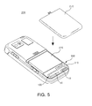
- FIG. 5 is a schematic perspective view illustrating a mobile communications terminal employing an electronic device case, according to an exemplary embodiment of the present invention
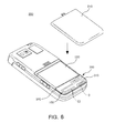
- FIG. 6 is a schematic perspective view illustrating a mobile communications terminal adopting an electronic device case provided with a coating layer, according to another exemplary embodiment of the present invention.
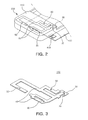
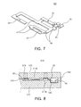
- FIG. 7 is a schematic perspective view illustrating a radiator provided to an electronic device case according to another exemplary embodiment of the present invention.
- FIG. 8 is a schematic cross-sectional view illustrating how a mold for manufacturing an electronic device case is filled with a resin material in order to manufacture an electronic device case, according to another exemplary embodiment of the present invention
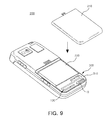
- FIG. 9 is a schematic perspective view illustrating a mobile communications terminal adopting an electronic device case, according to another exemplary embodiment of the present invention.
- FIG. 10 is a schematic perspective view illustrating a mobile communications terminal adopting an electronic device case provided with a coating layer, according to another exemplary embodiment of the present invention.
- FIG. 1 is a schematic perspective view illustrating a mobile communications terminal, an electronic device according to an exemplary embodiment of the invention
- FIG. 2 is a perspective view illustrating an electronic device case according to another exemplary embodiment of the invention.
- an electronic device case 300 may be placed inside a cover 210 of a mobile communications terminal 200, and the cover 210 may be a slim cover.
- the cover 210 may cover not only the electronic device case 300 but also a battery 220 and prevent the mobile communications terminal 200 from being damaged by an external shock.
- the electronic device case 300 may include a radiator 100 including an antenna pattern portion 10 and a connection terminal portion 30, and an electronic device case frame 310.
- connection terminal portion 30 may be connected to a terminal 410 of a circuit board 400.
- the electronic device case 300 may implement antenna performance for a mobile communications terminal 200.
- a coating layer 320 may be formed on the top surface of the electronic device case 300 in order to protect the radiator 100.
- the coating layer 320 is not an essential element in implementing the electronic device case 300 according to this exemplary embodiment of the invention.
- FIG. 3 is a schematic perspective view illustrating a radiator provided to an electronic device case according to another exemplary embodiment of the invention.
- FIG. 4 is a schematic cross-sectional view illustrating how a mold for manufacturing an electronic device case is filled with a resin material in order to manufacture an electronic device case, according to another exemplary embodiment of the invention.
- FIG. 5 is a schematic perspective view illustrating a mobile communications terminal adopting an electronic device case, according to an exemplary embodiment of the invention
- FIG. 6 is a schematic perspective view illustrating a mobile communications terminal including an electronic device case provided with a coating layer, according to another exemplary embodiment of the invention.
- the electronic device case 300 may include a radiator 100 having an antenna pattern portion 10 and a connection terminal portion 30, and an electronic device case frame 310.
- the radiator 100 may be formed of a conductive material such as aluminum, copper or the like to receive an external signal and sends the received signal to a signal processor of an electronic device, such as a mobile communications terminal 200. Furthermore, the radiator 100 may have an antenna pattern portion 10 forming a meander line in order to receive external signals with various bands.
- the antenna pattern portion 10 receives an external signal, and the connection terminal portion 30 is in contact with the circuit board of the electronic device to send the received external signal to the electronic device.
- the antenna pattern portion 10 and the connection terminal portion 30 may be arranged in different planes.
- the radiator 100 may have a three-dimensional structure by being bent in such a manner as to have a connection portion 20 connect the antenna pattern portion 10 and the connection terminal portion 30 to each other.
- connection portion 20 may be provided so as to position the antenna pattern portion 10 and the connection terminal portion 30 in different planes.
- the connection terminal portion 30, which is not embedded in the electronic device case 300, may be exposed to the opposite side 310b of the electronic device case 300 to one side 310a on which the antenna pattern portion 10 is formed.
- the radiator 100 may be bent such that the connection portion 20 connects the antenna pattern portion 10 with the connection terminal portion 30. In this way, the radiator 100 may have a three-dimensional curved shape.
- a radiator support portion 40 may protrude from the opposite side 310b of the electronic device case frame 310.
- the radiator support portion 40 may firmly support the connection portion 20 and the connection terminal portion 30 exposed to the opposite side 310b.
- connection terminal portion 30 transmits the received external signal to the electronic device.
- the connection terminal portions 224 may be formed by bending, forming or drawing a portion of the radiator 100.
- connection terminal portion 30 may be manufactured separately from the radiator 100, and then connected to the radiator 100 and connected to the terminal 410 of the circuit board 400.
- the antenna pattern portion 10 of the radiator 100 may have an insertion hole 50.
- the insertion hole 50 may serve to fix the radiator 100 to a mold 500 for injection-molding the electronic device case frame 310.
- a plurality of insertion holes 50 may be provided. Provided that the insertion hole 50 can fix the radiator 100 to the mold, the number and size of insertion holes 50 is not limited.
- the electronic device case frame 310 although being illustrated as having a flat portion in FIGS. 3 through 6 , may have a three-dimensional structure having a flat portion and a curved portion with a curvature.
- the radiator 100 may have flexibility so as to be disposed on the curved portion of the electronic device case frame 310.
- the electronic device case frame 310 is an injection-molded structure.
- the antenna pattern portion 10 is formed on the one side 310a of the electronic device case frame 310a, while the connection terminal portion 30 may be formed on the opposite side 310b to the one side 310a thereof.
- the radiator 100 after provided, may be placed in the internal space 530 within the mold 500.
- the internal space 530 is created when an upper mold 520 and a lower mold 510 are joined.
- a recess formed in the upper mold 520 or the lower mold 510 becomes the internal space 530 when the upper and lower molds 520 and 510 are joined.
- This fixation of the radiator 100 in the internal space 530 may reduce the occurrence of defects in the exterior of the electronic device case, and allow the radiator 100 to bear a high-temperature and high-pressure injection-molding solution.
- the coupling pin 525 may be formed of a magnet, and this magnetic coupling pin 525 may enhance support force fixing the radiator 100.
- the radiator 100 placed inside the internal space 530 comes into contact with the upper mold 520 due to the coupling pin 525, and the space between the radiator 100 and the lower mold 510 is filled with a resin material.
- a resin material injection hole 540 may be formed in the upper mold 520, the lower mold 510 or the upper and lower molds 520 and 510, such that the resin material can be introduced into the internal space 530 between the joined upper and lower molds 520 and 510 and applied to the radiator 100 to thereby form the electronic device case 300.
- the resin material introduced through the resin material injection hole 540, fills the space between the radiator 100 and the lower mold 510. In this way, the electronic device case 300, having the antenna pattern exposed on its outermost edge, can be manufactured.
- the antenna pattern portion 10, exposed on the outermost edge, may ensure the maximum utilization of a radiation volume, thereby realizing optimum radiations.
- a coating layer 320 may be formed on the top surface of the electronic device case 300 in order to protect the radiator 100.
- the coating layer 320 is not an essential element in implementing the electronic device case 300 according to an exemplary embodiment of the invention.
- the electronic device case 300 may further include a cover 210 contacting one side of the electronic device case frame 310 and forming the exterior of a body.
- a radiator support portion forming recess 540 may be provided in the internal space 530 between the upper and lower molds 520 and 510.
- the radiator support portion forming recess 540 accommodates the connection terminal portion 30, and allows for the formation of the radiator support portion 40 supporting the connection terminal portion 30.
- FIG. 7 is a schematic perspective view illustrating a radiator provided to an electronic device case according to another exemplary embodiment of the invention.
- FIG. 8 is a schematic cross-sectional view illustrating how a mold for manufacturing an electronic device case is filled with a resin material in order to manufacture an electronic device case, according to another exemplary embodiment of the invention.
- FIG. 9 is a schematic perspective view illustrating a mobile communications terminal adopting an electronic device case, according to another exemplary embodiment of the invention.
- FIG. 10 is a schematic perspective view illustrating a mobile communications terminal adopting an electronic device case provided with a coating layer, according to another exemplary embodiment of the invention.
- a radiator 100 provided in the electronic device case may include an exposed portion 60 in part of the antenna pattern portion 10.
- the electronic device case according to this exemplary embodiment is identical to that of the previous embodiment, except for the exposed portion 60. Therefore, a description regarding the identical part will be omitted.
- the exposed portion 60 may be formed by bending a portion of the antenna pattern portion 10 toward the outermost edge of the electronic device case frame 310 in a stepped manner.
- the formation of the exposed portion 60 is not limited only to the description, and may be changed by a person having ordinary skill in the art.
- the exposed portion 60 is not limited in terms of the number and the area thereof.
- the insertion hole 50 may be provided in the exposed portion 60.
- the insertion hole 50 may serve to fix the radiator 100 to the mold 500 for manufacturing the electronic device case frame 310 by injection-molding.
- a plurality of insertion holes 50 may be formed, and the number and size of the insertion holes 50 are not limited, provided that they can fix the radiator 100 to the mold 500.
- the coating layer 320 may be formed on the top surface of the electronic device case 300 in order to protect the radiator 100.
- the coating layer 320 is not an essential element in implementing the electronic device case 300 according to this exemplary embodiment.
- the electronic device case 300 may further include the cover 210 contacting one side of the electronic device case frame 310 and forming the exterior of a body.
- the coupling pin 525 formed in the mold 500 for manufacturing the electronic device case 300 is inserted into the insertion hole 50 formed in the antenna pattern portion 10 of the radiator 100, so that the radiator 100 comes into contact with the upper mold 520 and is fixed and supported by the internal space 530 of the mold 500, thereby reducing the occurrence of defects in the exterior and allowing the radiator 100 to bear a high-temperature and high-pressure injection-molding solution.
- the radiation volume can be utilized to a maximum extent, and the highest radiation characteristic can be implemented.
- the radiator is provided on the outermost edge such that the radiation volume can be utilized to a maximum extent, thereby implementing the optimum radiation characteristics.
- the radiator is stably fixed to the internal space of the mold, thereby reducing the occurrence of defects in the exterior of the molded electronic device case, and allowing the radiator to bear a high-temperature, high-pressure injection-molding solution.
Landscapes
- Engineering & Computer Science (AREA)
- Computer Networks & Wireless Communication (AREA)
- Telephone Set Structure (AREA)
- Support Of Aerials (AREA)
- Details Of Aerials (AREA)
Abstract
Description
- This application claims the priority of Korean Patent Application No.
10-2010-0022826 filed on March 15, 2010 - The present invention relates to an electronic device case, a mold for manufacturing the same, and a mobile communications terminal, and more particularly, to an electronic device case including a radiator on the outer side thereof, a mold for manufacturing the same, and a mobile communications terminal.
- Mobile communications terminals that support wireless communications, such as cellular phones, PDAs, navigation devices, laptop computers and the like, are indispensable in modern society. Mobile communications terminals have been developed to support functions including CDMA, wireless LAN, GSM, DMB and the like. One of the most important components enabling those functions is an antenna.
- Antennas, used for such mobile communications terminals, have advanced from external antennas, such as rod antennas or helical antennas, to internal antennas that are disposed inside terminals.
- The most important aspect in developing terminal antennas is to reduce these antennas in size and volume.
- In order to achieve the reduction in antenna size and volume, a variety of methods have been proposed to solve the spatial limitations of antennas, one of which involves forming an antenna integrally with a device.
- Here, the method of forming an antenna integrally with a device may include bonding a flexible antenna to a device by using adhesives, in-molding an antenna film by using In-mold labeling (IML), or generating and fusing an injection-molded protrusion.
- However, considering reliability and space utilization, the method of bonding an antenna by simply using adhesives may be limited in use.
- Furthermore, the method of in-molding an antenna film by using IML, although ensuring product reliability, is disadvantageous due to costly manufacturing processes and the occurrence of cosmetic defects.
- An aspect of the present invention provides an electronic device case, capable of realizing the highest radiation performance by having a radiator on the outermost portion thereof, and a mobile communications terminal including the same.
- An aspect of the present invention also provides a mold for manufacturing the electronic device case.
- An aspect of the present invention is also to reduce the occurrence of cosmetic defects by stably fixing a radiator to a mold for manufacturing an electronic device case when an electronic device case is produced in the mold.
- According to an aspect of the present invention, there is provided an electronic device case including: a radiator including an antenna pattern portion transmitting or receiving a signal, and a connection terminal portion transmitting the signal to or receiving the signal from a circuit board of an electronic device; and an electronic device case frame manufactured by subjecting the radiator to injection-molding, supporting the radiator and forming an exterior of the electronic device, wherein the antenna pattern portion includes an exposed portion exposed on the outermost edge of the electronic device case frame.
- The exposed portion may be formed in part of the antenna pattern portion.
- The exposed portion may include at least one insertion hole serving to fix the radiator to a mold for injection-molding the electronic device case frame.
- The exposed portion may be formed by bending the antenna pattern portion toward the outermost edge of the electronic device case frame in a stepped manner.
- The radiator may include a connection portion connecting the antenna pattern portion with the connection terminal portion as a part of the radiator. The connection portion may be formed such that the antenna pattern portion is arranged on one side of the electronic device case frame, and the connection terminal portion is arranged on the other side of the electronic device case frame, which is opposite to the one side thereof.
- The connection terminal portion may be in contact with and be supported by a radiator support portion protruding from the other side of the electronic device case frame, which is opposite to the one side on which the antenna pattern portion is arranged.
- The electronic device case frame may include a coating layer on the outermost surface thereof to protect the exposed portion.
- The electronic device case may further include a cover contacting one surface of the electronic device case frame and forming an exterior of a body.
- According to another aspect of the present invention, there is provided a mobile communications terminal including: an electronic device case including an electronic device case frame manufactured by subjecting a radiator including an antenna pattern portion and a connection terminal portion to injection-molding, wherein the antenna pattern portion includes an exposed portion exposed on the outermost edge of the electronic device case frame; and a circuit board connected to the connection terminal portion and receiving a signal from or transmitting a signal to the radiator.
- The exposed portion may be formed in part of the antenna pattern portion.
- The exposed portion may include at least one insertion hole serving to fix the radiator to a mold for injection-molding the electronic device case frame.
- The exposed portion may be formed by bending the antenna pattern portion toward the outermost edge of the electronic device case frame in a stepped manner.
- The radiator may include a connection portion connecting the antenna pattern portion with the connection terminal portion as a part of the radiator. The connection portion may be formed such that the antenna pattern portion is arranged on one side of the electronic device case frame, and the connection terminal portion is arranged on the other side of the electronic device case frame, which is opposite to the one side thereof.
- The connection terminal portion may be in contact with and is supported by a radiator support portion protruding from the other side of the electronic device case frame, which is opposite to the one side on which the antenna pattern portion is arranged.
- The electronic device case frame may include a coating layer on the outermost surface thereof to protect the exposed portion.
- The mobile communications terminal may further include a cover contacting one surface of the electronic device case frame and forming an exterior of a body.
- According to another aspect of the present invention, there is provided a mold for manufacturing an electronic device case, the mold including: an upper mold and a lower mold receiving a radiator including an antenna pattern portion receiving and transmitting a signal, a connection terminal portion contacting a circuit board of an electronic device, and a connection portion allowing the antenna pattern portion and the connection terminal portion to be arranged in difference planes; and a resin material injection portion formed in the upper mold, the lower mold or the upper and lower molds so that, when the upper and lower molds are joined, a resin material is injected into an internal space between the upper and lower molds through the resin material injection portion and is applied to the radiator to thereby form an electronic device case. The upper mold comes into contact with the radiator so that the antenna pattern portion is exposed on the outermost edge of the electronic device case, and the electronic device case including the radiator is formed in the internal space.
- The antenna pattern portion may include at least one insertion hole. The upper mold may include a coupling pin inserted into the insertion hole to fix the radiator in the internal space.
- The coupling pin may be formed of a magnet.
- The internal space between the upper and lower molds may receive the connection terminal portion, and a radiator support portion may be formed in the internal space to support the connection terminal portion.
- The above and other aspects, features and other advantages of the present invention will be more clearly understood from the following detailed description taken in conjunction with the accompanying drawings, in which:
-
FIG. 1 is a schematic perspective view illustrating a mobile communications terminal, an electronic device, according to an exemplary embodiment of the present invention; -
FIG. 2 is a perspective view illustrating an electronic device case according to another exemplary embodiment of the present invention; -
FIG. 3 is a schematic perspective view illustrating a radiator provided to an electronic device case according to another exemplary embodiment of the present invention; -
FIG. 4 is a schematic cross-sectional view illustrating how a mold for manufacturing an electronic device case is filled with a resin material for the manufacturing of an electronic device case, according to another exemplary embodiment of the present invention; -
FIG. 5 is a schematic perspective view illustrating a mobile communications terminal employing an electronic device case, according to an exemplary embodiment of the present invention; -
FIG. 6 is a schematic perspective view illustrating a mobile communications terminal adopting an electronic device case provided with a coating layer, according to another exemplary embodiment of the present invention; -
FIG. 7 is a schematic perspective view illustrating a radiator provided to an electronic device case according to another exemplary embodiment of the present invention; -
FIG. 8 is a schematic cross-sectional view illustrating how a mold for manufacturing an electronic device case is filled with a resin material in order to manufacture an electronic device case, according to another exemplary embodiment of the present invention; -
FIG. 9 is a schematic perspective view illustrating a mobile communications terminal adopting an electronic device case, according to another exemplary embodiment of the present invention; and -
FIG. 10 is a schematic perspective view illustrating a mobile communications terminal adopting an electronic device case provided with a coating layer, according to another exemplary embodiment of the present invention. - Exemplary embodiments of the present invention will now be described in detail with reference to the accompanying drawings. The invention may, however, be embodied in many different forms and should not be construed as being limited to the embodiments set forth herein. While those skilled in the art could readily devise many other varied embodiments that incorporate the teachings of the present invention through the addition, modification or deletion of elements, such embodiments may fall within the scope of the present inventior..
- The same or equivalent elements are referred to by the same reference numerals throughout the specification.
-
FIG. 1 is a schematic perspective view illustrating a mobile communications terminal, an electronic device according to an exemplary embodiment of the invention, andFIG. 2 is a perspective view illustrating an electronic device case according to another exemplary embodiment of the invention. - Referring to
FIGS. 1 and2 , anelectronic device case 300, according to an exemplary embodiment of the present invention, may be placed inside acover 210 of amobile communications terminal 200, and thecover 210 may be a slim cover. - Here, the
cover 210 may cover not only theelectronic device case 300 but also abattery 220 and prevent themobile communications terminal 200 from being damaged by an external shock. - The
electronic device case 300 may include aradiator 100 including anantenna pattern portion 10 and aconnection terminal portion 30, and an electronicdevice case frame 310. - The
connection terminal portion 30 may be connected to aterminal 410 of acircuit board 400. By this connection, theelectronic device case 300 may implement antenna performance for amobile communications terminal 200. - Furthermore, a
coating layer 320 may be formed on the top surface of theelectronic device case 300 in order to protect theradiator 100. However, thecoating layer 320 is not an essential element in implementing theelectronic device case 300 according to this exemplary embodiment of the invention. -
FIG. 3 is a schematic perspective view illustrating a radiator provided to an electronic device case according to another exemplary embodiment of the invention.FIG. 4 is a schematic cross-sectional view illustrating how a mold for manufacturing an electronic device case is filled with a resin material in order to manufacture an electronic device case, according to another exemplary embodiment of the invention.FIG. 5 is a schematic perspective view illustrating a mobile communications terminal adopting an electronic device case, according to an exemplary embodiment of the invention, andFIG. 6 is a schematic perspective view illustrating a mobile communications terminal including an electronic device case provided with a coating layer, according to another exemplary embodiment of the invention. - Referring to
FIGS. 3 ,5 and6 , theelectronic device case 300, according to another exemplary embodiment of the invention, may include aradiator 100 having anantenna pattern portion 10 and aconnection terminal portion 30, and an electronicdevice case frame 310. - The
radiator 100 may be formed of a conductive material such as aluminum, copper or the like to receive an external signal and sends the received signal to a signal processor of an electronic device, such as amobile communications terminal 200. Furthermore, theradiator 100 may have anantenna pattern portion 10 forming a meander line in order to receive external signals with various bands. - In the
radiator 100, theantenna pattern portion 10 receives an external signal, and theconnection terminal portion 30 is in contact with the circuit board of the electronic device to send the received external signal to the electronic device. Here, theantenna pattern portion 10 and theconnection terminal portion 30 may be arranged in different planes. - In addition, the
radiator 100 may have a three-dimensional structure by being bent in such a manner as to have aconnection portion 20 connect theantenna pattern portion 10 and theconnection terminal portion 30 to each other. - The
connection portion 20 may be provided so as to position theantenna pattern portion 10 and theconnection terminal portion 30 in different planes. Theconnection terminal portion 30, which is not embedded in theelectronic device case 300, may be exposed to theopposite side 310b of theelectronic device case 300 to oneside 310a on which theantenna pattern portion 10 is formed. - That is, the
radiator 100 may be bent such that theconnection portion 20 connects theantenna pattern portion 10 with theconnection terminal portion 30. In this way, theradiator 100 may have a three-dimensional curved shape. - In order to support the
radiator 100 having the three-dimensional curved shape, aradiator support portion 40 may protrude from theopposite side 310b of the electronicdevice case frame 310. - The
radiator support portion 40 may firmly support theconnection portion 20 and theconnection terminal portion 30 exposed to theopposite side 310b. - The
connection terminal portion 30 transmits the received external signal to the electronic device. The connection terminal portions 224 may be formed by bending, forming or drawing a portion of theradiator 100. - Furthermore, the
connection terminal portion 30 may be manufactured separately from theradiator 100, and then connected to theradiator 100 and connected to theterminal 410 of thecircuit board 400. - Here, the
antenna pattern portion 10 of theradiator 100 may have aninsertion hole 50. Theinsertion hole 50 may serve to fix theradiator 100 to amold 500 for injection-molding the electronicdevice case frame 310. - A plurality of insertion holes 50 may be provided. Provided that the
insertion hole 50 can fix theradiator 100 to the mold, the number and size of insertion holes 50 is not limited. - The electronic
device case frame 310, although being illustrated as having a flat portion inFIGS. 3 through 6 , may have a three-dimensional structure having a flat portion and a curved portion with a curvature. - The
radiator 100 may have flexibility so as to be disposed on the curved portion of the electronicdevice case frame 310. - The electronic
device case frame 310 is an injection-molded structure. Theantenna pattern portion 10 is formed on the oneside 310a of the electronicdevice case frame 310a, while theconnection terminal portion 30 may be formed on theopposite side 310b to the oneside 310a thereof. - Referring to
FIGS. 4 through 6 , theradiator 100, after provided, may be placed in theinternal space 530 within themold 500. - The
internal space 530 is created when anupper mold 520 and alower mold 510 are joined. In detail, a recess formed in theupper mold 520 or thelower mold 510 becomes theinternal space 530 when the upper andlower molds - When the
upper mold 520 and thelower mold 510 are joined, acoupling pin 525 formed on theupper mold 520 is inserted into theinsertion hole 50 formed in theradiator 100, so that theradiator 100 can be fixed in theinternal space 530. - This fixation of the
radiator 100 in theinternal space 530 may reduce the occurrence of defects in the exterior of the electronic device case, and allow theradiator 100 to bear a high-temperature and high-pressure injection-molding solution. - Here, the
coupling pin 525 may be formed of a magnet, and thismagnetic coupling pin 525 may enhance support force fixing theradiator 100. - That is, the
radiator 100 placed inside theinternal space 530 comes into contact with theupper mold 520 due to thecoupling pin 525, and the space between theradiator 100 and thelower mold 510 is filled with a resin material. - A resin
material injection hole 540 may be formed in theupper mold 520, thelower mold 510 or the upper andlower molds internal space 530 between the joined upper andlower molds radiator 100 to thereby form theelectronic device case 300. - The resin material, introduced through the resin
material injection hole 540, fills the space between theradiator 100 and thelower mold 510. In this way, theelectronic device case 300, having the antenna pattern exposed on its outermost edge, can be manufactured. - The
antenna pattern portion 10, exposed on the outermost edge, may ensure the maximum utilization of a radiation volume, thereby realizing optimum radiations. - Furthermore, a
coating layer 320 may be formed on the top surface of theelectronic device case 300 in order to protect theradiator 100. However, thecoating layer 320 is not an essential element in implementing theelectronic device case 300 according to an exemplary embodiment of the invention. - Also, the
electronic device case 300 may further include acover 210 contacting one side of the electronicdevice case frame 310 and forming the exterior of a body. - A radiator support
portion forming recess 540 may be provided in theinternal space 530 between the upper andlower molds portion forming recess 540 accommodates theconnection terminal portion 30, and allows for the formation of theradiator support portion 40 supporting theconnection terminal portion 30. -
FIG. 7 is a schematic perspective view illustrating a radiator provided to an electronic device case according to another exemplary embodiment of the invention.FIG. 8 is a schematic cross-sectional view illustrating how a mold for manufacturing an electronic device case is filled with a resin material in order to manufacture an electronic device case, according to another exemplary embodiment of the invention.FIG. 9 is a schematic perspective view illustrating a mobile communications terminal adopting an electronic device case, according to another exemplary embodiment of the invention.FIG. 10 is a schematic perspective view illustrating a mobile communications terminal adopting an electronic device case provided with a coating layer, according to another exemplary embodiment of the invention. - Referring to
FIGS. 7 to 10 , aradiator 100 provided in the electronic device case, according to another exemplary embodiment of the invention, may include an exposedportion 60 in part of theantenna pattern portion 10. - The electronic device case according to this exemplary embodiment is identical to that of the previous embodiment, except for the exposed
portion 60. Therefore, a description regarding the identical part will be omitted. - The exposed
portion 60 may be formed by bending a portion of theantenna pattern portion 10 toward the outermost edge of the electronicdevice case frame 310 in a stepped manner. However, the formation of the exposedportion 60 is not limited only to the description, and may be changed by a person having ordinary skill in the art. - Furthermore, the exposed
portion 60 is not limited in terms of the number and the area thereof. - The
insertion hole 50 may be provided in the exposedportion 60. Theinsertion hole 50 may serve to fix theradiator 100 to themold 500 for manufacturing the electronicdevice case frame 310 by injection-molding. - A plurality of insertion holes 50 may be formed, and the number and size of the insertion holes 50 are not limited, provided that they can fix the
radiator 100 to themold 500. - The
coating layer 320 may be formed on the top surface of theelectronic device case 300 in order to protect theradiator 100. However, thecoating layer 320 is not an essential element in implementing theelectronic device case 300 according to this exemplary embodiment. - The
electronic device case 300 may further include thecover 210 contacting one side of the electronicdevice case frame 310 and forming the exterior of a body. - As described in the above exemplary embodiments, the
coupling pin 525 formed in themold 500 for manufacturing theelectronic device case 300 is inserted into theinsertion hole 50 formed in theantenna pattern portion 10 of theradiator 100, so that theradiator 100 comes into contact with theupper mold 520 and is fixed and supported by theinternal space 530 of themold 500, thereby reducing the occurrence of defects in the exterior and allowing theradiator 100 to bear a high-temperature and high-pressure injection-molding solution. - Since at least a part of the
antenna pattern portion 10 is exposed on the outermost edge of the electronicdevice case frame 310, the radiation volume can be utilized to a maximum extent, and the highest radiation characteristic can be implemented. - As set forth above, according to the electronic device case, the mold for manufacturing the same and the mobile communications terminal according to exemplary embodiments of the invention, the radiator is provided on the outermost edge such that the radiation volume can be utilized to a maximum extent, thereby implementing the optimum radiation characteristics.
- Furthermore, when the electronic device case is molded, the radiator is stably fixed to the internal space of the mold, thereby reducing the occurrence of defects in the exterior of the molded electronic device case, and allowing the radiator to bear a high-temperature, high-pressure injection-molding solution.
- While the present invention has been shown and described in connection with the exemplary embodiments, it will be apparent to those skilled in the art that modifications and variations can be made without departing from the spirit and scope of the invention as defined by the appended claims.
Claims (20)
- An electronic device case comprising:a radiator including an antenna pattern portion transmitting or receiving a signal, and a connection terminal portion transmitting the signal to or receiving the signal from a circuit board of an electronic device; andan electronic device case frame manufactured by subjecting the radiator to injection-molding, supporting the radiator and forming an exterior of the electronic device,wherein the antenna pattern portion includes an exposed portion exposed on the outermost edge of the electronic device case frame.
- The electronic device case of claim 1, wherein the exposed portion is formed in part of the antenna pattern portion.
- The electronic device case of claim 1, wherein the exposed portion has at least one insertion hole serving to fix the radiator to a mold for injection-molding the electronic device case frame.
- The electronic device case of claim 1, wherein the exposed portion is formed by bending the antenna pattern portion toward the outermost edge of the electronic device case frame in a stepped manner.
- The electronic device case of claim 1, wherein the radiator includes a connection portion connecting the antenna pattern portion with the connection terminal portion as a part of the radiator,
wherein the connection portion is formed such that the antenna pattern portion is arranged on one side of the electronic device case frame, and the connection terminal portion is arranged on the other side of the electronic device case frame, which is opposite to the one side thereof. - The electronic device case of claim 1, wherein the connection terminal portion is in contact with and is supported by a radiator support portion protruding from the other side of the electronic device case frame, which is opposite to the one side on which the antenna pattern portion is arranged.
- The electronic device case of claim 1, wherein the electronic device case frame includes a coating layer on the outermost surface thereof to protect the exposed portion.
- The electronic device case of claim 1, further comprising a cover contacting one surface of the electronic device case frame and forming an exterior of a body.
- A mobile communications terminal comprising:an electronic device case including an electronic device case frame manufactured by subjecting a radiator including an antenna pattern portion and a connection terminal portion to injection-molding, wherein the antenna pattern portion includes an exposed portion exposed on the outermost edge of the electronic device case frame; anda circuit board connected to the connection terminal portion and receiving a signal from or transmitting a signal to the radiator.
- The mobile communications terminal of claim 9, wherein the exposed portion is formed in part of the antenna pattern portion.
- The mobile communications terminal of claim 9, wherein the exposed portion has at least one insertion hole serving to fix the radiator to a mold for injection-molding the electronic device case frame.
- The mobile communications terminal of claim 9, wherein the exposed portion is formed by bending the antenna pattern portion toward the outermost edge of the electronic device case frame in a stepped manner.
- The mobile communications terminal of claim 9, wherein the radiator includes a connection portion connecting the antenna pattern portion with the connection terminal portion as a part of the radiator,
wherein the connection portion is formed such that the antenna pattern portion is arranged on one side of the electronic device case frame, and the connection terminal portion is arranged on the other side of the electronic device case frame, which is opposite to the one side thereof. - The mobile communications terminal of claim 9, wherein the connection terminal portion is in contact with and is supported by a radiator support portion protruding from the other side of the electronic device case frame, which is opposite to the one side on which the antenna pattern portion is arranged.
- The mobile communications terminal of claim 9, wherein the electronic device case frame includes a coating layer on the outermost surface thereof to protect the exposed portion.
- The mobile communications terminal of claim 9, further comprising a cover contacting one surface of the electronic device case frame and forming an exterior of a body.
- A mold for manufacturing an electronic device case, the mold comprising:an upper mold and a lower mold receiving a radiator including an antenna pattern portion receiving and transmitting a signal, a connection terminal portion contacting a circuit board of an electronic device, and a connection portion allowing the antenna pattern portion and the connection terminal portion to be arranged in difference planes; anda resin material injection portion formed in the upper mold, the lower mold or the upper and lower molds so that, when the upper and lower molds are joined, a resin material is injected into an internal space between the upper and lower molds through the resin material injection portion and is applied to the radiator to thereby form an electronic device case,wherein the upper mold comes into contact with the radiator so that the antenna pattern portion is exposed on the outermost edge of the electronic device case, and the electronic device case including the radiator is formed in the internal space.
- The mold of claim 17, wherein the antenna pattern portion includes at least one insertion hole,
wherein the upper mold includes a coupling pin inserted into the insertion hole to fix the radiator in the internal space. - The mold of claim 17, wherein the coupling pin is formed of a magnet.
- The mold of claim 17, wherein the internal space between the upper and lower molds receives the connection terminal portion, and a radiator support portion is formed in the internal space to support the connection terminal portion.
Applications Claiming Priority (1)
| Application Number | Priority Date | Filing Date | Title |
|---|---|---|---|
| KR1020100022826A KR101101468B1 (en) | 2010-03-15 | 2010-03-15 | Electronic device case and manufacturing mold thereof, mobile communication terminal |
Publications (1)
| Publication Number | Publication Date |
|---|---|
| EP2367231A1 true EP2367231A1 (en) | 2011-09-21 |
Family
ID=44005025
Family Applications (1)
| Application Number | Title | Priority Date | Filing Date |
|---|---|---|---|
| EP11250288A Withdrawn EP2367231A1 (en) | 2010-03-15 | 2011-03-11 | Electronic device case, mold for manufacturing the same, and mobile communications terminal |
Country Status (5)
| Country | Link |
|---|---|
| US (1) | US20110222219A1 (en) |
| EP (1) | EP2367231A1 (en) |
| JP (1) | JP5655239B2 (en) |
| KR (1) | KR101101468B1 (en) |
| CN (1) | CN102195121A (en) |
Families Citing this family (10)
| Publication number | Priority date | Publication date | Assignee | Title |
|---|---|---|---|---|
| US8641402B2 (en) * | 2011-09-09 | 2014-02-04 | Cheng Uei Precision Industry Co., Ltd. | Injection mold |
| JP5988361B2 (en) * | 2012-07-27 | 2016-09-07 | 京セラ株式会社 | Electronics |
| US9332329B2 (en) * | 2012-09-28 | 2016-05-03 | Htc Corporation | Electronic apparatus |
| US9282668B2 (en) | 2012-09-28 | 2016-03-08 | Htc Corporation | Electronic apparatus and method for assembling the same |
| US9137918B2 (en) * | 2012-09-28 | 2015-09-15 | Htc Corporation | Electronic apparatus and method for assembling the same |
| WO2015165050A1 (en) * | 2014-04-29 | 2015-11-05 | 华为终端有限公司 | Antenna circuit, terminal device, and method for disposing antenna circuit |
| CN104332698B (en) * | 2014-07-09 | 2017-02-15 | 深圳盈达信息科技有限公司 | Monopole antenna with parasitic elements |
| KR20160107592A (en) * | 2015-03-04 | 2016-09-19 | 삼성전기주식회사 | Antenna pattern frame, electronic device including the same and manufacturing method of the same |
| EP3478040A4 (en) * | 2016-06-23 | 2020-02-26 | Toray Industries, Inc. | HOUSING AND METHOD FOR PRODUCING A HOUSING |
| KR102364470B1 (en) * | 2017-08-23 | 2022-02-18 | 삼성전자주식회사 | Electronic device comprising antenna |
Citations (5)
| Publication number | Priority date | Publication date | Assignee | Title |
|---|---|---|---|---|
| GB2345196A (en) * | 1998-12-23 | 2000-06-28 | Nokia Mobile Phones Ltd | An antenna and method of production |
| WO2004032280A2 (en) * | 2002-10-02 | 2004-04-15 | E-Tenna Corporation | Method of manufacturing antennas using micro-insert-molding techniques |
| US20070216583A1 (en) * | 2006-03-20 | 2007-09-20 | Lite-On Technology Corporation | Antenna structure for electronic device |
| US20090322629A1 (en) * | 2008-06-27 | 2009-12-31 | Asustek Computer Inc. | Cover for communication device and method for manufacturing the same |
| US20100039347A1 (en) * | 2008-08-15 | 2010-02-18 | Chi Mei Communication Systems, Inc. | Housing functioning as an antenna and method for fabricating the same |
Family Cites Families (18)
| Publication number | Priority date | Publication date | Assignee | Title |
|---|---|---|---|---|
| US5986609A (en) * | 1998-06-03 | 1999-11-16 | Ericsson Inc. | Multiple frequency band antenna |
| FI116334B (en) * | 2003-01-15 | 2005-10-31 | Lk Products Oy | Antenna element |
| US7080787B2 (en) * | 2003-07-03 | 2006-07-25 | Symbol Technologies, Inc. | Insert molded antenna |
| JP3981112B2 (en) * | 2004-10-28 | 2007-09-26 | 株式会社東芝 | Mobile device |
| JP4633605B2 (en) * | 2005-01-31 | 2011-02-16 | 富士通コンポーネント株式会社 | ANTENNA DEVICE AND ELECTRONIC DEVICE, ELECTRONIC CAMERA, ELECTRONIC CAMERA LIGHT EMITTING DEVICE, AND PERIPHERAL DEVICE |
| JP4754601B2 (en) * | 2005-01-31 | 2011-08-24 | 富士通コンポーネント株式会社 | Antenna device |
| JP2007221513A (en) * | 2006-02-17 | 2007-08-30 | Chant Sincere Co Ltd | Casing of wireless communication product with common antenna |
| WO2007094494A1 (en) * | 2006-02-19 | 2007-08-23 | Nissha Printing Co., Ltd. | Feeding structure of housing with antenna |
| KR20080025285A (en) * | 2006-09-15 | 2008-03-20 | 삼성전기주식회사 | Method for manufacturing case structure with antenna |
| JP2008072559A (en) * | 2006-09-15 | 2008-03-27 | Murata Mfg Co Ltd | Antenna system and manufacturing method thereof |
| KR20090006336A (en) * | 2007-07-11 | 2009-01-15 | 삼성전기주식회사 | Case integrated antenna and manufacturing method |
| JP4881247B2 (en) * | 2007-07-13 | 2012-02-22 | 株式会社東芝 | Electronic device and manufacturing method thereof |
| KR100905858B1 (en) * | 2007-08-21 | 2009-07-02 | 삼성전기주식회사 | Case integrated antenna and manufacturing method |
| TW200921986A (en) * | 2007-11-02 | 2009-05-16 | Delta Electronics Inc | Wireless communication device |
| US7663558B2 (en) * | 2007-12-12 | 2010-02-16 | Motorola, Inc. | Tag reader with conformal antenna stand |
| KR100910161B1 (en) * | 2009-02-25 | 2009-07-30 | 주식회사 에이티앤씨 | Built-in antenna integrated portable terminal case and manufacturing method thereof |
| KR100930207B1 (en) * | 2009-03-16 | 2009-12-07 | 삼성전기주식회사 | Manufacturing method of mobile communication terminal, mobile communication terminal case and mobile communication terminal using same |
| KR100935954B1 (en) * | 2009-04-23 | 2010-01-12 | 삼성전기주식회사 | Case of electronic device, method and mould for manufacturing the same, and mobile communication terminal |
-
2010
- 2010-03-15 KR KR1020100022826A patent/KR101101468B1/en not_active Expired - Fee Related
-
2011
- 2011-02-28 JP JP2011042720A patent/JP5655239B2/en not_active Expired - Fee Related
- 2011-03-02 US US13/038,776 patent/US20110222219A1/en not_active Abandoned
- 2011-03-11 EP EP11250288A patent/EP2367231A1/en not_active Withdrawn
- 2011-03-15 CN CN2011100641721A patent/CN102195121A/en active Pending
Patent Citations (5)
| Publication number | Priority date | Publication date | Assignee | Title |
|---|---|---|---|---|
| GB2345196A (en) * | 1998-12-23 | 2000-06-28 | Nokia Mobile Phones Ltd | An antenna and method of production |
| WO2004032280A2 (en) * | 2002-10-02 | 2004-04-15 | E-Tenna Corporation | Method of manufacturing antennas using micro-insert-molding techniques |
| US20070216583A1 (en) * | 2006-03-20 | 2007-09-20 | Lite-On Technology Corporation | Antenna structure for electronic device |
| US20090322629A1 (en) * | 2008-06-27 | 2009-12-31 | Asustek Computer Inc. | Cover for communication device and method for manufacturing the same |
| US20100039347A1 (en) * | 2008-08-15 | 2010-02-18 | Chi Mei Communication Systems, Inc. | Housing functioning as an antenna and method for fabricating the same |
Also Published As
| Publication number | Publication date |
|---|---|
| KR101101468B1 (en) | 2012-01-03 |
| US20110222219A1 (en) | 2011-09-15 |
| CN102195121A (en) | 2011-09-21 |
| JP2011193455A (en) | 2011-09-29 |
| JP5655239B2 (en) | 2015-01-21 |
| KR20110103656A (en) | 2011-09-21 |
Similar Documents
| Publication | Publication Date | Title |
|---|---|---|
| US20110222219A1 (en) | Electronic device case, mold for manufacturing the same, and mobile communications terminal | |
| US20110205141A1 (en) | Antenna pattern frame and mold for manufacturing electronic device case including the same | |
| US8643547B2 (en) | Antenna pattern frame, method and mold for manufacturing the same, electronic device case having antenna pattern frame embedded therein, and method for manufacturing the same | |
| US8982009B2 (en) | Antenna pattern frame, method and mold for manufacturing the same, and electronic device | |
| US9705188B2 (en) | Antenna pattern frame and method and mold for manufacturing the same | |
| US8618989B2 (en) | Electronic device case, method and mold for manufacturing the same, and mobile communications terminal | |
| US8289216B2 (en) | Antenna-embedded case for mobile communications terminal, method of manufacturing the same, and mobile communications terminal | |
| US8442603B2 (en) | Method of manufacturing case for mobile communications terminal, case for mobile communications terminal, and mobile communications terminal having the same | |
| EP2421089A2 (en) | Electronic device having antenna pattern embedded in case and method for manufacturing the same | |
| US20140205708A1 (en) | Antenna pattern frame, case of electronic device and mould for manufacturing the same | |
| EP2403065A2 (en) | Electronic device case having antenna pattern embedded therein, method for manufacturing the same, mold for manufacturing antenna pattern frame, and electronic device | |
| JP5951540B2 (en) | Method for manufacturing electronic device case including antenna pattern frame, and method for manufacturing electronic device including electronic device case | |
| CN105048083A (en) | Antenna pattern frame and method of manufacturing the same | |
| US20110291899A1 (en) | Antenna radiator, method of manufacturing electronic device case having plurality of antenna pattern radiators embedded therein, and electronic device case | |
| KR101113346B1 (en) | method and mould for manufacturing case of electronic device having antenna radiation device embeded therein | |
| EP2520406A2 (en) | Communications terminal and method of manufacturing the same | |
| KR20130051054A (en) | Mobile device case with built-in antenna and manufacturing method of the same | |
| KR101025941B1 (en) | Antenna radiator and manufacturing method of antenna pattern frame using same | |
| KR20130059590A (en) | Case of electronic device and mould for manufacturing the same, and mobile communication terminal |
Legal Events
| Date | Code | Title | Description |
|---|---|---|---|
| PUAI | Public reference made under article 153(3) epc to a published international application that has entered the european phase |
Free format text: ORIGINAL CODE: 0009012 |
|
| 17P | Request for examination filed |
Effective date: 20110324 |
|
| AK | Designated contracting states |
Kind code of ref document: A1 Designated state(s): AL AT BE BG CH CY CZ DE DK EE ES FI FR GB GR HR HU IE IS IT LI LT LU LV MC MK MT NL NO PL PT RO RS SE SI SK SM TR |
|
| AX | Request for extension of the european patent |
Extension state: BA ME |
|
| RIN1 | Information on inventor provided before grant (corrected) |
Inventor name: PARK, HYUN DO Inventor name: HAN, CHANG MOK Inventor name: LIM, DAE KI Inventor name: JEON, DAE SEONG Inventor name: SUNG, JAE SUK Inventor name: AN, CHAN GWANG Inventor name: NAM, HYUN KIL Inventor name: LEE, DAE KYU Inventor name: CHO, SUNG EUN Inventor name: BAE, SANG WOO |
|
| 17Q | First examination report despatched |
Effective date: 20120928 |
|
| STAA | Information on the status of an ep patent application or granted ep patent |
Free format text: STATUS: THE APPLICATION IS DEEMED TO BE WITHDRAWN |
|
| 18D | Application deemed to be withdrawn |
Effective date: 20160705 |