EP2367199A2 - Plasma etching method, plasma etching apparatus, and computer-readable storage medium - Google Patents
Plasma etching method, plasma etching apparatus, and computer-readable storage medium Download PDFInfo
- Publication number
- EP2367199A2 EP2367199A2 EP11157855A EP11157855A EP2367199A2 EP 2367199 A2 EP2367199 A2 EP 2367199A2 EP 11157855 A EP11157855 A EP 11157855A EP 11157855 A EP11157855 A EP 11157855A EP 2367199 A2 EP2367199 A2 EP 2367199A2
- Authority
- EP
- European Patent Office
- Prior art keywords
- film
- plasma etching
- amorphous carbon
- sion
- upper electrode
- Prior art date
- Legal status (The legal status is an assumption and is not a legal conclusion. Google has not performed a legal analysis and makes no representation as to the accuracy of the status listed.)
- Withdrawn
Links
Images




Classifications
-
- H—ELECTRICITY
- H10—SEMICONDUCTOR DEVICES; ELECTRIC SOLID-STATE DEVICES NOT OTHERWISE PROVIDED FOR
- H10P—GENERIC PROCESSES OR APPARATUS FOR THE MANUFACTURE OR TREATMENT OF DEVICES COVERED BY CLASS H10
- H10P50/00—Etching of wafers, substrates or parts of devices
- H10P50/73—Etching of wafers, substrates or parts of devices using masks for insulating materials
-
- H—ELECTRICITY
- H01—ELECTRIC ELEMENTS
- H01J—ELECTRIC DISCHARGE TUBES OR DISCHARGE LAMPS
- H01J37/00—Discharge tubes with provision for introducing objects or material to be exposed to the discharge, e.g. for the purpose of examination or processing thereof
- H01J37/32—Gas-filled discharge tubes
- H01J37/32009—Arrangements for generation of plasma specially adapted for examination or treatment of objects, e.g. plasma sources
- H01J37/32082—Radio frequency generated discharge
- H01J37/32091—Radio frequency generated discharge the radio frequency energy being capacitively coupled to the plasma
-
- H—ELECTRICITY
- H10—SEMICONDUCTOR DEVICES; ELECTRIC SOLID-STATE DEVICES NOT OTHERWISE PROVIDED FOR
- H10P—GENERIC PROCESSES OR APPARATUS FOR THE MANUFACTURE OR TREATMENT OF DEVICES COVERED BY CLASS H10
- H10P14/00—Formation of materials, e.g. in the shape of layers or pillars
- H10P14/60—Formation of materials, e.g. in the shape of layers or pillars of insulating materials
- H10P14/65—Formation of materials, e.g. in the shape of layers or pillars of insulating materials characterised by treatments performed before or after the formation of the materials
- H10P14/6502—Formation of materials, e.g. in the shape of layers or pillars of insulating materials characterised by treatments performed before or after the formation of the materials of treatments performed before formation of the materials
- H10P14/6512—Formation of materials, e.g. in the shape of layers or pillars of insulating materials characterised by treatments performed before or after the formation of the materials of treatments performed before formation of the materials by exposure to a gas or vapour
- H10P14/6514—Formation of materials, e.g. in the shape of layers or pillars of insulating materials characterised by treatments performed before or after the formation of the materials of treatments performed before formation of the materials by exposure to a gas or vapour by exposure to a plasma
-
- H—ELECTRICITY
- H10—SEMICONDUCTOR DEVICES; ELECTRIC SOLID-STATE DEVICES NOT OTHERWISE PROVIDED FOR
- H10P—GENERIC PROCESSES OR APPARATUS FOR THE MANUFACTURE OR TREATMENT OF DEVICES COVERED BY CLASS H10
- H10P14/00—Formation of materials, e.g. in the shape of layers or pillars
- H10P14/60—Formation of materials, e.g. in the shape of layers or pillars of insulating materials
- H10P14/69—Inorganic materials
- H10P14/692—Inorganic materials composed of oxides, glassy oxides or oxide-based glasses
- H10P14/6921—Inorganic materials composed of oxides, glassy oxides or oxide-based glasses containing silicon
- H10P14/6922—Inorganic materials composed of oxides, glassy oxides or oxide-based glasses containing silicon the material containing Si, O and at least one of H, N, C, F or other non-metal elements, e.g. SiOC, SiOC:H or SiONC
- H10P14/6927—Inorganic materials composed of oxides, glassy oxides or oxide-based glasses containing silicon the material containing Si, O and at least one of H, N, C, F or other non-metal elements, e.g. SiOC, SiOC:H or SiONC the material being a silicon oxynitride, e.g. SiON or SiON:H
-
- H—ELECTRICITY
- H10—SEMICONDUCTOR DEVICES; ELECTRIC SOLID-STATE DEVICES NOT OTHERWISE PROVIDED FOR
- H10P—GENERIC PROCESSES OR APPARATUS FOR THE MANUFACTURE OR TREATMENT OF DEVICES COVERED BY CLASS H10
- H10P50/00—Etching of wafers, substrates or parts of devices
- H10P50/20—Dry etching; Plasma etching; Reactive-ion etching
- H10P50/24—Dry etching; Plasma etching; Reactive-ion etching of semiconductor materials
- H10P50/242—Dry etching; Plasma etching; Reactive-ion etching of semiconductor materials of Group IV materials
-
- H—ELECTRICITY
- H10—SEMICONDUCTOR DEVICES; ELECTRIC SOLID-STATE DEVICES NOT OTHERWISE PROVIDED FOR
- H10P—GENERIC PROCESSES OR APPARATUS FOR THE MANUFACTURE OR TREATMENT OF DEVICES COVERED BY CLASS H10
- H10P50/00—Etching of wafers, substrates or parts of devices
- H10P50/20—Dry etching; Plasma etching; Reactive-ion etching
- H10P50/26—Dry etching; Plasma etching; Reactive-ion etching of conductive or resistive materials
- H10P50/264—Dry etching; Plasma etching; Reactive-ion etching of conductive or resistive materials by chemical means
- H10P50/266—Dry etching; Plasma etching; Reactive-ion etching of conductive or resistive materials by chemical means by vapour etching only
- H10P50/267—Dry etching; Plasma etching; Reactive-ion etching of conductive or resistive materials by chemical means by vapour etching only using plasmas
-
- H—ELECTRICITY
- H10—SEMICONDUCTOR DEVICES; ELECTRIC SOLID-STATE DEVICES NOT OTHERWISE PROVIDED FOR
- H10P—GENERIC PROCESSES OR APPARATUS FOR THE MANUFACTURE OR TREATMENT OF DEVICES COVERED BY CLASS H10
- H10P50/00—Etching of wafers, substrates or parts of devices
- H10P50/20—Dry etching; Plasma etching; Reactive-ion etching
- H10P50/28—Dry etching; Plasma etching; Reactive-ion etching of insulating materials
- H10P50/282—Dry etching; Plasma etching; Reactive-ion etching of insulating materials of inorganic materials
- H10P50/283—Dry etching; Plasma etching; Reactive-ion etching of insulating materials of inorganic materials by chemical means
-
- H—ELECTRICITY
- H10—SEMICONDUCTOR DEVICES; ELECTRIC SOLID-STATE DEVICES NOT OTHERWISE PROVIDED FOR
- H10P—GENERIC PROCESSES OR APPARATUS FOR THE MANUFACTURE OR TREATMENT OF DEVICES COVERED BY CLASS H10
- H10P76/00—Manufacture or treatment of masks on semiconductor bodies, e.g. by lithography or photolithography
- H10P76/20—Manufacture or treatment of masks on semiconductor bodies, e.g. by lithography or photolithography of masks comprising organic materials
- H10P76/204—Manufacture or treatment of masks on semiconductor bodies, e.g. by lithography or photolithography of masks comprising organic materials of organic photoresist masks
- H10P76/2041—Photolithographic processes
Definitions
- the present invention relates to a plasma etching method, a plasma etching apparatus and a computer-readable storage medium.
- a plasma etching process is performed by using, e.g., a photoresist or the like as a mask, to thereby form an etching target film such as a silicon oxide film or the like in a desired pattern.
- the plasma etching apparatus there is known, e.g., a capacitively coupled plasma etching apparatus for generating a plasma by applying a RF (radio frequency) power between a lower electrode also serving as a mounting table for mounting thereon a substrate such as a semiconductor wafer and an upper electrode disposed to face the lower electrode.
- a film thickness of a mask tends to be decreased while the depth of the hole is increased, so that it is difficult to obtain a vertical hole shape.
- the present invention provides a plasma etching method capable of performing etching for forming a hole having a large depth in a desired shape, a plasma etching apparatus and a computer-readable storage medium.
- a plasma etching method for plasma-etching a silicon oxide film or a silicon nitride film formed below an amorphous carbon film by using a pattern of the amorphous carbon film as a final mask in a multilayer mask including a photoresist layer having a predetermined pattern, an organic bottom anti-reflection coating (BARC) film formed below the photoresist layer, an SiON film formed below the BARC film, and the amorphous carbon film formed below the SiON film.
- BARC organic bottom anti-reflection coating
- An initial mask used at the time when the plasma etching of the silicon oxide film or the silicon nitride film is started is under a state in which the SiON film remains on the amorphous carbon film and a ratio of a film thickness of the amorphous carbon film to a film thickness of the residual SiON film is smaller than or equal to about 14.
- a plasma etching method capable of performing etching for forming a hole having a large depth in a desired shape, a plasma etching apparatus and a computer-readable storage medium.
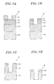
- Figs. 1A to 1D show an enlarged view showing cross sectional configurations of a semiconductor wafer as a target substrate in a plasma etching method in accordance with an embodiment of the preset invention.
- Fig. 2 shows a configuration of a plasma etching apparatus in accordance with an embodiment of the present invention. First of all, the configuration of the plasma processing apparatus will be described with reference to Fig. 2 .
- the plasma etching apparatus includes an airtight processing chamber 1 that is electrically grounded.
- the processing chamber 1 is formed in a cylindrical shape and is made of, e.g., aluminum or the like.
- a mounting table 2 for horizontally supporting a semiconductor wafer W as a target substrate.
- the mounting table 2 is made of, e.g., aluminum or the like, and serves as a lower electrode.
- the mounting table 2 is supported by a conductive supporting table 4 provided via an insulating plate 3.
- a focus ring 5 formed of, e.g., single crystalline silicon, is provided on an upper peripheral portion of the mounting table 2.
- a cylindrical inner wall member 3a made of, e.g., quartz or the like, is provided to surround the mounting table 2 and the supporting table 4.
- the mounting table 2 is connected to a first RF (radio frequency) power supply 10a through a first matching unit 11a, and is connected to a second RF power supply 10b through a second matching unit 11b.
- the first RF power supply 10a is used for plasma generation, and a RF power of a predetermined frequency (about 27 MHz or higher, e.g., about 40 MHz) is supplied from the first RF power supply 10a to the mounting table 2.
- the second RF power supply 10b is used for ion attraction (bias), and a RF power of a predetermined frequency (about 13.56 MHz or less, e.g., about 2 MHz) lower than that of the RF power from the first RF power supply 10a is supplied from the second RF power supply 10b to the mounting table 2.
- a shower head 16 serving as an upper electrode is disposed above the mounting table 2 to face the mounting table 2 in parallel.
- the mounting table 2 and the shower head 16 serve as a pair of electrodes (upper electrode and lower electrode).
- an electrostatic chuck 6 for electrostatically attracting and holding the semiconductor wafer W.
- the electrostatic chuck 6 is formed by embedding an electrode 6a in an insulator 6b, and the electrode 6a is connected to a DC power supply 12. Further, by applying a DC voltage from the DC power supply 12 to the electrode 6a, the semiconductor wafer W is attracted and held by a Coulomb force.
- a coolant path 4a is formed inside the supporting table 4, and is connected to a coolant inlet line 4b and a coolant outlet line 4c.
- an appropriate coolant e.g., cooling water or the like
- the supporting table 4 and the mounting table 2 can be controlled at a predetermined temperature.
- a backside gas supply line 30 for supplying a cold heat transfer gas (backside gas) to the backside of the semiconductor wafer W is provided to extend through the mounting table 2 and the like.
- the backside gas supply line 30 is connected to a backside gas supply source (not shown).
- the shower head 16 is provided at an upper portion of the processing chamber 1.
- the shower head 16 has a main body 16a and an upper top plate 16b forming an electrode plate, and is supported at the upper portion of the processing chamber 1 via an insulation member 45.
- the main body 16a is made of a conductive material, e.g., aluminum having an anodically oxidized surface, and the upper top plate 16b is detachably held on the bottom of the main body 16a.
- a gas diffusion space 16c is provided inside the main body 16a, and a plurality of gas holes 16d are formed in the bottom of the main body 16a so as to be positioned at the bottom of the gas diffusion space 16c.
- gas injection holes 16e are provided in the upper top plate 16b to extend through the upper top plate 16b in the thickness direction thereof and communicate with the respective gas holes 16d.
- a processing gas supplied to the gas diffusion space 16c is supplied and diffused in the processing chamber 1 in a shower shape through the gas holes 16d and the gas injection holes 16e.
- the main body 16a and the like are provided with lines (not shown) for circulating a coolant, so that the shower head 16 can be cooled to a desired temperature during the plasma etching process.
- a gas inlet port 16f for introducing a processing gas into the gas diffusion space 16c.
- the gas inlet port 16f is connected to one end of a gas supply line 15a, and the other end of the gas supply line 15a is connected to a processing gas supply source 15 for supplying a processing gas for etching or treatment.
- the gas supply line 15a is provided with a mass flow controller (MFC) 15b and an opening/closing valve V1 disposed thereon in that order from the upstream side.
- MFC mass flow controller
- V1 opening/closing valve
- the processing gas for plasma etching is supplied from the processing gas supply source 15 to the gas diffusion space 16c through the gas supply line 15a, and then is supplied to the processing chamber 1 in a shower shape through the gas holes 16d and the gas injection holes 16e.
- a variable DC power supply 52 is electrically connected to the shower head 16 serving as the upper electrode via a low pass filter (LPF) 51.
- the power supply of the variable DC power supply 52 can be on-off controlled by an on/off switch 53.
- a current and a voltage of the variable DC power supply 52 and an on/off operation of the on/off switch 53 are controlled by a control unit 60 to be described later.
- the on/off switch 53 is turned on by the control unit 60 if necessary, and a predetermined negative DC voltage, for example, is applied to the shower head 16 serving as the upper electrode.
- a cylindrical ground conductor 1a extends upward from the sidewall of the processing chamber 1 so as to be located at a position higher than the height position of the shower head 16.
- the cylindrical ground conductor 1a has a ceiling wall at the top thereof.
- a gas exhaust port 71 is formed at the bottom of the processing chamber 1, and a gas exhaust unit 73 is connected to the gas exhaust port 71.
- a vacuum pump provided in the gas exhaust unit 73, the inside of the processing chamber 1 can be depressurized to a predetermined vacuum level.
- a loading/unloadlng port 74 for the wafer W is provided at a sidewall of the processing chamber 1, and a gate valve 75 for opening or closing the loading/unloading port 74 is provided at the loading/unloading port 74.
- Reference numerals 76 and 77 in the drawing denote deposition shield members that are detachably installed.
- the deposition shield member 76 is provided along the inner wall surface of the processing chamber 1, and prevents etching by-products (deposits) from being attached to the processing chamber 1.
- a conductive port (GND block) 79 DC-connected to the ground is provided to a portion of the deposition shield member 76 at a height position substantially same as the height of the semiconductor wafer W. Accordingly, an abnormal discharge can be prevented.
- the operation of the plasma etching apparatus configured as described above is generally controlled by a control unit 60.
- the control unit 60 has a process controller 61 which has a CPU and controls each unit of the plasma etching apparatus, a user interface 62 and a storage unit 63.
- the user interface 62 includes a keyboard for a process manager to input commands to operate the plasma etching apparatus, a display for visualizing an operational status of the plasma etching apparatus, and the like.
- the storage unit 63 stores therein recipes including a control program (software), processing condition data and the like for realizing various processes performed by the plasma etching apparatus under the control of the process controller 61. Moreover, when a command is received from the user interface 62, a necessary recipe is retrieved from the storage unit 63 and executed by the process controller 61, so that a desired process is performed by the plasma etching apparatus under the control of the process controller 61. Further, the recipes including the control program, the processing condition data and the like can be stored in a computer-readable storage medium (for example, a hard disk, a CD, a flexible disk, a semiconductor memory, or the like) or can be transmitted on-line, when needed, from another apparatus, via, e.g., a dedicated line.
- a control program software
- processing condition data and the like for realizing various processes performed by the plasma etching apparatus under the control of the process controller 61.
- the gate valve 75 is opened, and the semiconductor wafer W is loaded through the loading/unloading port 74 into the processing chamber 1 by a transfer robot (not shown) or the like from a load lock chamber (not shown), and then is mounted on the mounting table 2. Thereafter, the transfer robot is retreated from the processing chamber 1, and the gate valve 75 is closed. Then, the processing chamber 1 is evacuated by the vacuum pump of the gas exhaust unit 73 through the gas exhaust port 71.
- a predetermined processing gas (etching gas) is introduced from the processing gas supply source 15 into the processing chamber 1, and the inside of the processing chamber 1 is maintained at a predetermined pressure level.
- a RF power having a frequency of, e.g., about 40 MHz is supplied from the first RF power supply 10a to the mounting table 2.
- a RF power having a frequency of, e.g., about 3 MHz, for ion attraction is supplied from the second RF power supply 10b to the mounting table 2.
- a predetermined DC voltage is applied from the DC power supply 12 to the electrode 6a of the electrostatic chuck 6, and the semiconductor wafer W is electrostatically attracted and held on the electrostatic chuck 6 by a Coulomb force.
- an electric field is formed between the shower head 16 serving as the upper electrode and the mounting table 2 serving as the lower electrode.
- a discharge is generated in a processing space in which the semiconductor wafer W exists, and the silicon oxide film or the silicon nitride film, the amorphous carbon film, the SiON film, the organic bottom anti-reflection coating (BARC) film and the like formed on the semiconductor wafer W are etched by the plasma of the processing gas which is generated by the discharge.
- a plasma having a high electron density and a low ion energy may be required. If a DC voltage is used in that case, energy of ions striking the semiconductor wafer W is suppressed, and the electron density of the plasma is increased. As a consequence, an etching rate of an etching target film formed on the semiconductor wafer W is increased, and a sputtering rate of a film serving as a mask formed on the etching target film is reduced, which results in improvement of selectivity. Further, the photoresist layer is hardened, so that the residual amount of the photoresist layer can be increased.
- the supply of the RF powers, the supply of the DC voltage and the supply of the processing gas are stopped, and the semiconductor wafer W is unloaded from the processing chamber 1 in the reverse sequence as described above.
- FIGs. 1A to 1D are enlarged views showing cross sectional configurations of principal parts of a semiconductor wafer W as a target substrate in the present embodiment.
- a photoresist layer 101 patterned in a predetermined shape i.e., a photoresist layer 101 having holes formed at predetermined positions, is formed as an uppermost layer of the semiconductor wafer W.
- An organic bottom anti-reflection coating (BARC) film 102 is formed below the photoresist layer 101; a SiON film 103 is formed below the organic BART film 102; and an amorphous carbon film 104 is formed below the SiON film 103.
- BARC organic bottom anti-reflection coating
- a silicon oxide film (or a silicon nitride film) 105 as an etching target film is formed below the amorphous carbon film 104.
- the photoresist layer 101, the organic BARC film 102, the SiON film 103 and the amorphous carbon film 104 which are formed above the silicon oxide film 105 form a multilayer mask.
- the semiconductor wafer W having the above-described structure is accommodated in the processing chamber 1 of the plasma etching apparatus shown in Fig. 2 and then is mounted on the mounting table 2.
- the organic BARC film 102 and the SiON film 103 are etched by using the photoresist layer 101 as an initial mask from the state shown in Fig. 1A , thereby obtaining a state shown in Fig. 1B .
- the residual amount (film thickness) of the photoresist layer 101 exceeds a certain level.
- the amorphous carbon film 104 is etched by using the residual photoresist layer 101 and the etched organic BARC film 102 and the etched SiON film 103 as a mask, thereby obtaining a state shown in Fig. 1C .
- the silicon oxide film (or the silicon nitride film) 105 is etched by using the amorphous carbon film 104 as a mask.
- the silicon oxide film (or the silicon nitride film) 105 has a thickness of about 2500 nm or above. In this embodiment, the thickness thereof is about 2600 nm.
- Fig. 1C shows a state of the initial mask used at the time when the etching of the silicon oxide film 105 is started.
- the initial mask is under a state in which the SiON film 103 remains on the amorphous carbon film 104 (having a thickness of about 850 nm in the present embodiment).
- the ratio of the film thickness of the amorphous carbon film 104 to the film thickness of the residual SiON film 103 is set as follow:
- the initial mask used at the time when the etching of the silicon oxide film 105 is started in the present embodiment includes the amorphous carbon film 104 having a thickness of about 850 nm and the residual SiON film having a thickness of about 60.0 nm or above, preferably about 62.5 nm or above, which remains on the amorphous carbon film 104. Accordingly, as shown in Fig. 1D , a film thickness (residual amount) of the amorphous carbon film 104 remaining after the completion of the etching of the silicon oxide film 105 can be increased, and the silicon oxide film 105 can be etched in a desired shape.
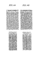
- Figs. 3A and 3B provide electron microscope images showing the states of the wafer at the time when the etching of the silicon oxide film 105 is completed in a test example, wherein Fig. 3A shows a central portion of the wafer, and Fig. 2B shows a peripheral portion of the wafer.
- the lower electron microscope image is an enlarged view around openings shown in the upper electron microscope image.
- the ratio of the film thickness of the amorphous carbon film 104 to the film thickness (residual amount in thickness) of the residual SiON film 103 is about 13.6.
- the film thickness (residual amount) of the amorphous carbon film 104 in Fig. 3A is about 645 nm
- the film thickness (residual amount) of the amorphous carbon film 104 in Fig. 3B is about 600 nm.
- the hole in the silicon oxide film 105 has a substantially vertical shape, which can prevent the occurrence of bowing or the like.
- the ratio of the film thickness of the amorphous carbon film 104 to the film thickness (residual amount in thickness) of the residual SiON film 103 is preferably about 14 or less.
- Figs. 4A and 4B provide electron microscope images showing the state of the wafer at the time when the etching of the silicon oxide film 105 is completed in a comparative example, wherein Fig. 4A shows a central portion of the wafer, and Fig. 4B shows a peripheral portion of the wafer.
- the lower electron microscope image is an enlarged view around openings shown in the upper electron microscope image.
- the ratio of the film thickness of the amorphous carbon film 104 to the film thickness of the residual SiON film 103 is about 17.
- the film thickness (residual amount) of the amorphous carbon film 104 in Fig. 4A is about 595 nm
- the film thickness (residual amount) of the amorphous carbon film 104 in Fig. 4B is about 545 nm.
- the film thickness (residual amount) of the amorphous carbon film 104 is smaller than about 600 nm, which is smaller than that in the test example, so that bowing occurred in the hole of the silicon oxide film 105.
- the residual amount of the amorphous carbon film 104 in the test example and that in the comparative example have a difference of about 50 nm.
- Fig. 5 shows relationship between the increased amount in thickness of the residual amorphous carbon film and the increased amount in thickness of the residual SiON film 103 in the initial mask at the time when the etching of the silicon oxide film 105 is started.
- the film thickness (residual amount) of the SiON film in the initial mask needs to be increased by about 10 to 15 nm in order to increase the film thickness of the amorphous carbon film 104 by about 40 to 60 nm.
- the plasma etching was performed in accordance with the following recipes. These recipes are read out from the storage unit 63 of the control unit 60 and sent to the process controller 61.
- the process controller 61 controls each unit of the plasma etching apparatus based on the control program, thereby performing the plasma etching process in accordance with the read-out recipes.
- DC voltage -1100 V (The applied DC voltage ranges from about -400 V to about -1100 V in accordance with the condition of the applied RF power.)
- the RF power is reduced to about 300 M/300 W, and the flow rate of O 2 gas is reduced to about 10 sccm. Accordingly, the etch selectivity to the photoresist layer 101 can be improved, and the residual amount of the SiON film 103 at the time when the etching of the amorphous carbon film 104 is completed can be increased to about 60 nm or above. Further, when the RF power was set to, e.g., about 1500 W/1500 W, and the flow rate of O 2 gas was set to about 30 sccm, the residual amount of the SiON film 103 was reduced to about 55 nm.
- the organic BARC film 102 and the SiON film 103 are etched, it is preferable to apply a DC voltage to the upper electrode. If the etching is performed while applying a DC voltage to the upper electrode, the photoresist layer 102 is hardened and, thus, the residual amount thereof can be increased. This becomes more effective when the gap between the upper electrode and the lower electrode (mounting table) is reduced to, e.g., about 30 mm. For that reason, it is preferable to apply a DC voltage to the upper electrode in a state where the gap between the upper electrode and the lower electrode (mounting table) is reduced.
- Figs. 6A to 6C provide electron microscope images showing relationship between the residual amount of the mask and the application of a DC voltage to the upper electrode in case of etching a silicon oxide film.
- the electron microscope image of Fig. 6A shows a case in which a DC voltage of about -1050 V is applied; that of Fig. 6B shows a case in which a DC voltage of about -600 V is applied; and that of Fig. 6C shows a case in which no DC voltage is applied.
- the upper electron microscope images illustrate the states of the top surface of the semiconductor wafer, and the lower electron microscope images illustrate the vertical cross sectional configuration of the semiconductor wafer.
- the residual amount of the mask can be improved by about 60 nm and about 83 nm, respectively, compared to when no DC voltage was applied.
- the example shown in Figs. 6A to 6C shows the case of etching the silicon oxide film, the same result can be obtained in the case of etching the organic BARC film or the like by using a carbon fluoride etching gas.
- the organic BARC film is etched by using an etching gas containing a large amount of oxygen.
- oxygen in the etching gas reacts with silicon of the upper electrode, thereby forming a silicon oxide film. Since the silicon oxide film is an insulating film, the function of the upper electrode deteriorates. By reducing the amount of oxygen in the etching gas, however, the formation of the silicon oxide film can be suppressed even when a DC voltage is applied.
- the amorphous carbon film 104 that is an organic film is etched without applying a DC voltage to the upper electrode.
- the photoresist layer 101 and the organic BARC film 102 are also etched. Therefore, the amorphous carbon film 104 is etched by using the SiON film 103 as a mask.
- the residual amount of the photoresist layer 101 during the etching of the organic BARC film 102 and the SiON film 103 the residual amount of the SiON film 103 can be increased.
- the residual amount of the SiON film 303 upon completing the etching of the amorphous carbon film 104 can be increased by increasing a pressure to, e.g., about 6.65 Pa (50 mTorr).
- the silicon oxide film 105 When the silicon oxide film 105 is etched, it is preferable to apply a DC voltage to the upper electrode. Further, generally, the silicon oxide film 105 is etched by using a processing gas generating large amount of deposits to obtain a high selectivity of the silicon oxide film 105 against the amorphous carbon film 104. However, in the present embodiment, the initial mask in which the SiON film 103 having a large thickness remains on the amorphous carbon film 104 is used, so that the etching can be performed under the condition in which deposits are reduced. Hence, a hole having a desired shape can be formed while improving an etching profile.
- bottom distortion in which a shape of a bottom portion of the hole is distorted may occur.
- the bottom distortion can be prevented by setting a temperature of the mounting table (lower electrode) for mounting thereon a semiconductor wafer W to about 40 °C.
Landscapes
- Physics & Mathematics (AREA)
- Engineering & Computer Science (AREA)
- Plasma & Fusion (AREA)
- Chemical & Material Sciences (AREA)
- Analytical Chemistry (AREA)
- Drying Of Semiconductors (AREA)
Abstract
A plasma etching method is provided to perform a plasma etching on a silicon oxide film or a silicon nitride film formed below an amorphous carbon film by using a pattern of the amorphous carbon film as a final mask in a multilayer mask including a photoresist layer having a predetermined pattern, an organic bottom anti-reflection coating (BARC) film formed below the photoresist layer, an SiON film formed below the BARC film, and the amorphous carbon film formed below the SiON film. An initial mask used at the time when the plasma etching of the silicon oxide film or the silicon nitride film is started is under a state in which the SiON film remains on the amorphous carbon film and a ratio of a film thickness of the amorphous carbon film to a film thickness of the residual SiON film is smaller than or equal to about 14.
Description
- The present invention relates to a plasma etching method, a plasma etching apparatus and a computer-readable storage medium.
- In a conventional semiconductor device manufacturing process, a plasma etching process is performed by using, e.g., a photoresist or the like as a mask, to thereby form an etching target film such as a silicon oxide film or the like in a desired pattern. As for the plasma etching apparatus, there is known, e.g., a capacitively coupled plasma etching apparatus for generating a plasma by applying a RF (radio frequency) power between a lower electrode also serving as a mounting table for mounting thereon a substrate such as a semiconductor wafer and an upper electrode disposed to face the lower electrode.
- In such plasma etching for forming a hole in an insulating film such as a silicon oxide film, a silicon nitride film or the like, a film thickness of a mask tends to be decreased while the depth of the hole is increased, so that it is difficult to obtain a vertical hole shape.
- Thus, various developments are being made in order to obtain desired opening characteristics and selectivity in the plasma etching process. For example, there is proposed a technique for obtaining desired opening characteristics and selectivity by applying a DC voltage to the upper electrode in the capacitively coupled plasma etching apparatus (see, e.g., Patent Document 1).
- Patent Document 1: Japanese Patent Application Publication No.
2008-21791 - As described above, it is required to develop a technique capable of performing etching for forming a hole having a large depth in a desired shape in the plasma etching process.
- In view of the above, the present invention provides a plasma etching method capable of performing etching for forming a hole having a large depth in a desired shape, a plasma etching apparatus and a computer-readable storage medium.
- In accordance with an embodiment of the present invention, there is provided a plasma etching method for plasma-etching a silicon oxide film or a silicon nitride film formed below an amorphous carbon film by using a pattern of the amorphous carbon film as a final mask in a multilayer mask including a photoresist layer having a predetermined pattern, an organic bottom anti-reflection coating (BARC) film formed below the photoresist layer, an SiON film formed below the BARC film, and the amorphous carbon film formed below the SiON film.
- An initial mask used at the time when the plasma etching of the silicon oxide film or the silicon nitride film is started is under a state in which the SiON film remains on the amorphous carbon film and a ratio of a film thickness of the amorphous carbon film to a film thickness of the residual SiON film is smaller than or equal to about 14.
- In accordance with the present invention, it is possible to provide a plasma etching method capable of performing etching for forming a hole having a large depth in a desired shape, a plasma etching apparatus and a computer-readable storage medium.
- The objects and features of the present invention will become apparent from the following description of embodiments, given in conjunction with the accompanying drawings, in which:
-
Figs. 1A to 1D show cross sectional configurations of a semiconductor wafer in a plasma etching method in accordance with an embodiment of the present invention; -
Fig. 2 shows a schematic configuration of a plasma etching apparatus in accordance with an embodiment of the present invention; -
Figs. 3A and 3B are electron microscope images showing a state of a semiconductor wafer in a test example; -
Figs. 4A and 4B are electron microscope images showing a state of a semiconductor wafer in a comparative example; -
Fig. 5 is a graph showing relationship between a residual amount of a SiON film and a residual amount of an amorphous carbon film; and -
Figs. 6A to 6C are electron microscope images showing changes in a state of a photoresist due to application of a DC voltage. - Embodiments of the present invention will be described with reference to the accompanying drawings which form a part hereof.
Figs. 1A to 1D show an enlarged view showing cross sectional configurations of a semiconductor wafer as a target substrate in a plasma etching method in accordance with an embodiment of the preset invention.Fig. 2 shows a configuration of a plasma etching apparatus in accordance with an embodiment of the present invention. First of all, the configuration of the plasma processing apparatus will be described with reference toFig. 2 . - The plasma etching apparatus includes an
airtight processing chamber 1 that is electrically grounded. Theprocessing chamber 1 is formed in a cylindrical shape and is made of, e.g., aluminum or the like. Provided in theprocessing chamber 1 is a mounting table 2 for horizontally supporting a semiconductor wafer W as a target substrate. The mounting table 2 is made of, e.g., aluminum or the like, and serves as a lower electrode. The mounting table 2 is supported by a conductive supporting table 4 provided via aninsulating plate 3. Further, afocus ring 5 formed of, e.g., single crystalline silicon, is provided on an upper peripheral portion of the mounting table 2. Furthermore, a cylindricalinner wall member 3a made of, e.g., quartz or the like, is provided to surround the mounting table 2 and the supporting table 4. - The mounting table 2 is connected to a first RF (radio frequency)
power supply 10a through afirst matching unit 11a, and is connected to a secondRF power supply 10b through asecond matching unit 11b. The firstRF power supply 10a is used for plasma generation, and a RF power of a predetermined frequency (about 27 MHz or higher, e.g., about 40 MHz) is supplied from the firstRF power supply 10a to the mounting table 2. Further, the secondRF power supply 10b is used for ion attraction (bias), and a RF power of a predetermined frequency (about 13.56 MHz or less, e.g., about 2 MHz) lower than that of the RF power from the firstRF power supply 10a is supplied from the secondRF power supply 10b to the mounting table 2. Meanwhile, ashower head 16 serving as an upper electrode is disposed above the mounting table 2 to face the mounting table 2 in parallel. The mounting table 2 and theshower head 16 serve as a pair of electrodes (upper electrode and lower electrode). - Provided on the top surface of the mounting table 2 is an
electrostatic chuck 6 for electrostatically attracting and holding the semiconductor wafer W. Theelectrostatic chuck 6 is formed by embedding anelectrode 6a in aninsulator 6b, and theelectrode 6a is connected to aDC power supply 12. Further, by applying a DC voltage from theDC power supply 12 to theelectrode 6a, the semiconductor wafer W is attracted and held by a Coulomb force. - A
coolant path 4a is formed inside the supporting table 4, and is connected to acoolant inlet line 4b and acoolant outlet line 4c. By circulating an appropriate coolant, e.g., cooling water or the like, through thecoolant path 4a, the supporting table 4 and the mounting table 2 can be controlled at a predetermined temperature. Moreover, a backsidegas supply line 30 for supplying a cold heat transfer gas (backside gas) to the backside of the semiconductor wafer W is provided to extend through the mounting table 2 and the like. The backsidegas supply line 30 is connected to a backside gas supply source (not shown). With such configuration, the semiconductor wafer W electrostatically held on the top surface of the mounting table 2 by theelectrostatic chuck 6 can be controlled to a predetermined temperature. - The
shower head 16 is provided at an upper portion of theprocessing chamber 1. Theshower head 16 has amain body 16a and anupper top plate 16b forming an electrode plate, and is supported at the upper portion of theprocessing chamber 1 via aninsulation member 45. Themain body 16a is made of a conductive material, e.g., aluminum having an anodically oxidized surface, and theupper top plate 16b is detachably held on the bottom of themain body 16a. - A
gas diffusion space 16c is provided inside themain body 16a, and a plurality ofgas holes 16d are formed in the bottom of themain body 16a so as to be positioned at the bottom of thegas diffusion space 16c. In addition,gas injection holes 16e are provided in theupper top plate 16b to extend through theupper top plate 16b in the thickness direction thereof and communicate with therespective gas holes 16d. With such configurations, a processing gas supplied to thegas diffusion space 16c is supplied and diffused in theprocessing chamber 1 in a shower shape through thegas holes 16d and thegas injection holes 16e. Besides, themain body 16a and the like are provided with lines (not shown) for circulating a coolant, so that theshower head 16 can be cooled to a desired temperature during the plasma etching process. - Formed in the
main body 16a is agas inlet port 16f for introducing a processing gas into thegas diffusion space 16c. Thegas inlet port 16f is connected to one end of agas supply line 15a, and the other end of thegas supply line 15a is connected to a processinggas supply source 15 for supplying a processing gas for etching or treatment. Thegas supply line 15a is provided with a mass flow controller (MFC) 15b and an opening/closing valve V1 disposed thereon in that order from the upstream side. Further, the processing gas for plasma etching is supplied from the processinggas supply source 15 to thegas diffusion space 16c through thegas supply line 15a, and then is supplied to theprocessing chamber 1 in a shower shape through thegas holes 16d and thegas injection holes 16e. - A variable
DC power supply 52 is electrically connected to theshower head 16 serving as the upper electrode via a low pass filter (LPF) 51. The power supply of the variableDC power supply 52 can be on-off controlled by an on/offswitch 53. A current and a voltage of the variableDC power supply 52 and an on/off operation of the on/offswitch 53 are controlled by acontrol unit 60 to be described later. As will be described later, when a plasma is generated in a processing space by applying the RF powers from the firstRF power supply 10a and the secondRF power supply 10b to the mounting table 2, the on/offswitch 53 is turned on by thecontrol unit 60 if necessary, and a predetermined negative DC voltage, for example, is applied to theshower head 16 serving as the upper electrode. - A cylindrical ground conductor 1a extends upward from the sidewall of the
processing chamber 1 so as to be located at a position higher than the height position of theshower head 16. The cylindrical ground conductor 1a has a ceiling wall at the top thereof. - A
gas exhaust port 71 is formed at the bottom of theprocessing chamber 1, and agas exhaust unit 73 is connected to thegas exhaust port 71. By operating a vacuum pump provided in thegas exhaust unit 73, the inside of theprocessing chamber 1 can be depressurized to a predetermined vacuum level. Meanwhile, a loading/unloadlng port 74 for the wafer W is provided at a sidewall of theprocessing chamber 1, and agate valve 75 for opening or closing the loading/unloading port 74 is provided at the loading/unloading port 74. -
Reference numerals deposition shield member 76 is provided along the inner wall surface of theprocessing chamber 1, and prevents etching by-products (deposits) from being attached to theprocessing chamber 1. A conductive port (GND block) 79 DC-connected to the ground is provided to a portion of thedeposition shield member 76 at a height position substantially same as the height of the semiconductor wafer W. Accordingly, an abnormal discharge can be prevented. - The operation of the plasma etching apparatus configured as described above is generally controlled by a
control unit 60. Thecontrol unit 60 has aprocess controller 61 which has a CPU and controls each unit of the plasma etching apparatus, auser interface 62 and astorage unit 63. - The
user interface 62 includes a keyboard for a process manager to input commands to operate the plasma etching apparatus, a display for visualizing an operational status of the plasma etching apparatus, and the like. - The
storage unit 63 stores therein recipes including a control program (software), processing condition data and the like for realizing various processes performed by the plasma etching apparatus under the control of theprocess controller 61. Moreover, when a command is received from theuser interface 62, a necessary recipe is retrieved from thestorage unit 63 and executed by theprocess controller 61, so that a desired process is performed by the plasma etching apparatus under the control of theprocess controller 61. Further, the recipes including the control program, the processing condition data and the like can be stored in a computer-readable storage medium (for example, a hard disk, a CD, a flexible disk, a semiconductor memory, or the like) or can be transmitted on-line, when needed, from another apparatus, via, e.g., a dedicated line. - Hereinafter, there will be described a process sequence of plasma-etching a silicon oxide film or a silicon nitride film, an amorphous carbon film, a SiON film, an organic bottom anti-reflection coating (BARC) film and the like formed on the semiconductor wafer W, which is performed by the plasma etching apparatus configured as described above. First, the
gate valve 75 is opened, and the semiconductor wafer W is loaded through the loading/unloading port 74 into theprocessing chamber 1 by a transfer robot (not shown) or the like from a load lock chamber (not shown), and then is mounted on the mounting table 2. Thereafter, the transfer robot is retreated from theprocessing chamber 1, and thegate valve 75 is closed. Then, theprocessing chamber 1 is evacuated by the vacuum pump of thegas exhaust unit 73 through thegas exhaust port 71. - After the inside of the
processing chamber 1 reaches a predetermined vacuum level, a predetermined processing gas (etching gas) is introduced from the processinggas supply source 15 into theprocessing chamber 1, and the inside of theprocessing chamber 1 is maintained at a predetermined pressure level. In this state, a RF power having a frequency of, e.g., about 40 MHz, is supplied from the firstRF power supply 10a to the mounting table 2. Further, a RF power having a frequency of, e.g., about 3 MHz, for ion attraction is supplied from the secondRF power supply 10b to the mounting table 2. At this time, a predetermined DC voltage is applied from theDC power supply 12 to theelectrode 6a of theelectrostatic chuck 6, and the semiconductor wafer W is electrostatically attracted and held on theelectrostatic chuck 6 by a Coulomb force. - In this case, due to the application of the RF powers to the mounting table 2 serving as the lower electrode as described above, an electric field is formed between the
shower head 16 serving as the upper electrode and the mounting table 2 serving as the lower electrode. A discharge is generated in a processing space in which the semiconductor wafer W exists, and the silicon oxide film or the silicon nitride film, the amorphous carbon film, the SiON film, the organic bottom anti-reflection coating (BARC) film and the like formed on the semiconductor wafer W are etched by the plasma of the processing gas which is generated by the discharge. - Since a DC voltage can be applied to the
shower head 16 during the plasma process as described above, the following effects are obtained. - Depending on a process involved, a plasma having a high electron density and a low ion energy may be required. If a DC voltage is used in that case, energy of ions striking the semiconductor wafer W is suppressed, and the electron density of the plasma is increased. As a consequence, an etching rate of an etching target film formed on the semiconductor wafer W is increased, and a sputtering rate of a film serving as a mask formed on the etching target film is reduced, which results in improvement of selectivity. Further, the photoresist layer is hardened, so that the residual amount of the photoresist layer can be increased.
- Upon the completion of the etching process, the supply of the RF powers, the supply of the DC voltage and the supply of the processing gas are stopped, and the semiconductor wafer W is unloaded from the
processing chamber 1 in the reverse sequence as described above. - Hereinafter, a plasma etching method in accordance with an embodiment of the present invention will be described with reference to
Figs. 1A to 1D. Figs. 1A to 1D are enlarged views showing cross sectional configurations of principal parts of a semiconductor wafer W as a target substrate in the present embodiment. As shown inFig. 1A , aphotoresist layer 101 patterned in a predetermined shape, i.e., aphotoresist layer 101 having holes formed at predetermined positions, is formed as an uppermost layer of the semiconductor wafer W. - An organic bottom anti-reflection coating (BARC)
film 102 is formed below thephotoresist layer 101; aSiON film 103 is formed below theorganic BART film 102; and anamorphous carbon film 104 is formed below theSiON film 103. - A silicon oxide film (or a silicon nitride film) 105 as an etching target film is formed below the
amorphous carbon film 104. Thephotoresist layer 101, theorganic BARC film 102, theSiON film 103 and theamorphous carbon film 104 which are formed above thesilicon oxide film 105 form a multilayer mask. - The semiconductor wafer W having the above-described structure is accommodated in the
processing chamber 1 of the plasma etching apparatus shown inFig. 2 and then is mounted on the mounting table 2. First of all, theorganic BARC film 102 and theSiON film 103 are etched by using thephotoresist layer 101 as an initial mask from the state shown inFig. 1A , thereby obtaining a state shown inFig. 1B . At this time, it is preferable that the residual amount (film thickness) of thephotoresist layer 101 exceeds a certain level. - Next, the
amorphous carbon film 104 is etched by using theresidual photoresist layer 101 and the etchedorganic BARC film 102 and theetched SiON film 103 as a mask, thereby obtaining a state shown inFig. 1C . Finally, the silicon oxide film (or the silicon nitride film) 105 is etched by using theamorphous carbon film 104 as a mask. The silicon oxide film (or the silicon nitride film) 105 has a thickness of about 2500 nm or above. In this embodiment, the thickness thereof is about 2600 nm. -
Fig. 1C shows a state of the initial mask used at the time when the etching of thesilicon oxide film 105 is started. The initial mask is under a state in which theSiON film 103 remains on the amorphous carbon film 104 (having a thickness of about 850 nm in the present embodiment). - In the present embodiment, the ratio of the film thickness of the
amorphous carbon film 104 to the film thickness of theresidual SiON film 103 is set as follow: - Film thickness of the
amorphous carbon film 104 / Film. thickness of the residual SiON film ≤ 14,
and preferably - Film thickness of the
amorphous carbon film 104 / Film thickness of the residual SiON film ≤ 13.6. - In other words, the initial mask used at the time when the etching of the
silicon oxide film 105 is started in the present embodiment includes theamorphous carbon film 104 having a thickness of about 850 nm and the residual SiON film having a thickness of about 60.0 nm or above, preferably about 62.5 nm or above, which remains on theamorphous carbon film 104. Accordingly, as shown inFig. 1D , a film thickness (residual amount) of theamorphous carbon film 104 remaining after the completion of the etching of thesilicon oxide film 105 can be increased, and thesilicon oxide film 105 can be etched in a desired shape. -
Figs. 3A and 3B provide electron microscope images showing the states of the wafer at the time when the etching of thesilicon oxide film 105 is completed in a test example, whereinFig. 3A shows a central portion of the wafer, andFig. 2B shows a peripheral portion of the wafer. The lower electron microscope image is an enlarged view around openings shown in the upper electron microscope image. - In the test example, in the initial mask used at the time when the etching of the
silicon oxide film 105 is started, the ratio of the film thickness of theamorphous carbon film 104 to the film thickness (residual amount in thickness) of theresidual SiON film 103 is about 13.6. In this case, the film thickness (residual amount) of theamorphous carbon film 104 inFig. 3A is about 645 nm, and the film thickness (residual amount) of theamorphous carbon film 104 inFig. 3B is about 600 nm. If the film thickness (residual amount) of theamorphous carbon film 104 remaining on thesilicon oxide film 105 at the time when the etching is completed is increased, the hole in thesilicon oxide film 105 has a substantially vertical shape, which can prevent the occurrence of bowing or the like. Moreover, the ratio of the film thickness of theamorphous carbon film 104 to the film thickness (residual amount in thickness) of theresidual SiON film 103 is preferably about 14 or less. -
Figs. 4A and 4B provide electron microscope images showing the state of the wafer at the time when the etching of thesilicon oxide film 105 is completed in a comparative example, whereinFig. 4A shows a central portion of the wafer, andFig. 4B shows a peripheral portion of the wafer. The lower electron microscope image is an enlarged view around openings shown in the upper electron microscope image. - In the comparative example, in the initial mask used at the time when the etching of the
silicon oxide film 105 is started, the ratio of the film thickness of theamorphous carbon film 104 to the film thickness of theresidual SiON film 103 is about 17. In this case, the film thickness (residual amount) of theamorphous carbon film 104 inFig. 4A is about 595 nm, and the film thickness (residual amount) of theamorphous carbon film 104 inFig. 4B is about 545 nm. As described above, in the comparative example, the film thickness (residual amount) of theamorphous carbon film 104 is smaller than about 600 nm, which is smaller than that in the test example, so that bowing occurred in the hole of thesilicon oxide film 105. - The residual amount of the
amorphous carbon film 104 in the test example and that in the comparative example have a difference of about 50 nm.Fig. 5 shows relationship between the increased amount in thickness of the residual amorphous carbon film and the increased amount in thickness of theresidual SiON film 103 in the initial mask at the time when the etching of thesilicon oxide film 105 is started. As shown inFig. 5 , the film thickness (residual amount) of the SiON film in the initial mask needs to be increased by about 10 to 15 nm in order to increase the film thickness of theamorphous carbon film 104 by about 40 to 60 nm. - In the above test example, the plasma etching was performed in accordance with the following recipes. These recipes are read out from the
storage unit 63 of thecontrol unit 60 and sent to theprocess controller 61. Theprocess controller 61 controls each unit of the plasma etching apparatus based on the control program, thereby performing the plasma etching process in accordance with the read-out recipes. - Processing gas: CF4/CHF3/C4F8/O2 = 240/60/10/10 sccm
- Pressure: 16.0 Pa (120 mTorr)
- DC voltage: -1100 V (The applied DC voltage ranges from about -400 V to about -1100 V in accordance with the condition of the applied RF power.)
- RF power (HF/LF): 300/300 W
- Temperature (upper/sidewall/lower): 95/60/0 °C
- Time: 80 sec
- Processing gas: O2/COS = 740/5 sccm
- Pressure: 2.66 Pa (20 mTorr)
- RF power (HF/LF): 2800/3000 W
- Temperature (upper/sidewall/lower): 95/60/0 °C
- Time: 40 sec
- Processing gas: C4F8/Ar/O2 = 60/450/59 sccm
- Pressure: 2.66 Pa (20 mTorr)
- RF power (HF/LF): 2000/4500 W
- DC voltage: -1100V
- Temperature (upper/sidewall/lower): 95/60/0 °C
- When the
organic BARC film 102 and theSiON film 103 are etched, the RF power is reduced to about 300 M/300 W, and the flow rate of O2 gas is reduced to about 10 sccm. Accordingly, the etch selectivity to thephotoresist layer 101 can be improved, and the residual amount of theSiON film 103 at the time when the etching of theamorphous carbon film 104 is completed can be increased to about 60 nm or above. Further, when the RF power was set to, e.g., about 1500 W/1500 W, and the flow rate of O2 gas was set to about 30 sccm, the residual amount of theSiON film 103 was reduced to about 55 nm. - In addition, when the
organic BARC film 102 and theSiON film 103 are etched, it is preferable to apply a DC voltage to the upper electrode. If the etching is performed while applying a DC voltage to the upper electrode, thephotoresist layer 102 is hardened and, thus, the residual amount thereof can be increased. This becomes more effective when the gap between the upper electrode and the lower electrode (mounting table) is reduced to, e.g., about 30 mm. For that reason, it is preferable to apply a DC voltage to the upper electrode in a state where the gap between the upper electrode and the lower electrode (mounting table) is reduced. -
Figs. 6A to 6C provide electron microscope images showing relationship between the residual amount of the mask and the application of a DC voltage to the upper electrode in case of etching a silicon oxide film. The electron microscope image ofFig. 6A shows a case in which a DC voltage of about -1050 V is applied; that ofFig. 6B shows a case in which a DC voltage of about -600 V is applied; and that ofFig. 6C shows a case in which no DC voltage is applied. InFigs. 6A to 6C , the upper electron microscope images illustrate the states of the top surface of the semiconductor wafer, and the lower electron microscope images illustrate the vertical cross sectional configuration of the semiconductor wafer. - As shown in
Figs. 6A to 6C , when a DC voltage of about -600 V and that of about -1050 V are applied to the upper electrode, the residual amount of the mask can be improved by about 60 nm and about 83 nm, respectively, compared to when no DC voltage was applied. Although the example shown inFigs. 6A to 6C shows the case of etching the silicon oxide film, the same result can be obtained in the case of etching the organic BARC film or the like by using a carbon fluoride etching gas. - The following etching conditions are applied to the example of
Fig. 6 . - Processing gas: C4F8/C4F6/C3F8/Ar/O2 = 37/5/28/450/59 sccm
- Pressure: 3.99 Pa (30 mTorr)
- RF power (HF/LF): 1500/4500 W
- Time: 60 sec
- In general, the organic BARC film is etched by using an etching gas containing a large amount of oxygen. When a DC voltage is applied to the upper electrode while the etching gas containing a large amount of oxygen is used, oxygen in the etching gas reacts with silicon of the upper electrode, thereby forming a silicon oxide film. Since the silicon oxide film is an insulating film, the function of the upper electrode deteriorates. By reducing the amount of oxygen in the etching gas, however, the formation of the silicon oxide film can be suppressed even when a DC voltage is applied.
- Meanwhile, the
amorphous carbon film 104 that is an organic film is etched without applying a DC voltage to the upper electrode. When theamorphous carbon film 104 is etched, thephotoresist layer 101 and theorganic BARC film 102 are also etched. Therefore, theamorphous carbon film 104 is etched by using theSiON film 103 as a mask. However, by increasing the residual amount of thephotoresist layer 101 during the etching of theorganic BARC film 102 and theSiON film 103, the residual amount of theSiON film 103 can be increased. Further, when theamorphous carbon film 104 is etched, the residual amount of the SiON film 303 upon completing the etching of theamorphous carbon film 104 can be increased by increasing a pressure to, e.g., about 6.65 Pa (50 mTorr). - When the
silicon oxide film 105 is etched, it is preferable to apply a DC voltage to the upper electrode. Further, generally, thesilicon oxide film 105 is etched by using a processing gas generating large amount of deposits to obtain a high selectivity of thesilicon oxide film 105 against theamorphous carbon film 104. However, in the present embodiment, the initial mask in which theSiON film 103 having a large thickness remains on theamorphous carbon film 104 is used, so that the etching can be performed under the condition in which deposits are reduced. Hence, a hole having a desired shape can be formed while improving an etching profile. - When a hole having a large depth is formed, bottom distortion in which a shape of a bottom portion of the hole is distorted may occur. In this case, the bottom distortion can be prevented by setting a temperature of the mounting table (lower electrode) for mounting thereon a semiconductor wafer W to about 40 °C.
- As described above, in accordance with the present embodiment and the test example, even a hole having a large depth can be etched in a desired shape while preventing the occurrence of bowing or the like.
- While the invention has been shown and described with respect to the embodiment or test example, it will be understood by those skilled in the art that various changes and modification may be made without departing from the scope of the invention as defined in the following claims.
Claims (6)
- A plasma etching method for performing a plasma etching on a silicon oxide film or a silicon nitride film formed below an amorphous carbon film by using a pattern of the amorphous carbon film as a final mask in a multilayer mask including a photoresist layer having a predetermined pattern, an organic bottom anti-reflection coating (BARC) film formed below the photoresist layer, an SiON film formed below the BARC film, and the amorphous carbon film formed below the SiON film,
wherein an initial mask used at the time when the plasma etching of the silicon oxide film or the silicon nitride film is started is under a state in which the SiON film remains on the amorphous carbon film and a ratio of a film thickness of the amorphous carbon film to a film thickness of the residual SiON film is smaller than or equal to about 14. - The plasma etching method of claim 1, wherein a plasma etching apparatus is used, the plasma etching apparatus including: a lower electrode, provided in a processing chamber, for mounting thereon a substrate; an upper electrode provided in the processing chamber to face the lower electrode; and a RF power supply for applying a RF power between the lower electrode and the upper electrode,
and wherein the organic bottom anti-reflection film and the SiON film are etched while a DC voltage is applied to the upper electrode. - The plasma etching method of claim 2, wherein the plasma etching of the amorphous carbon film is performed while no a DC voltage is applied to the upper electrode.
- The plasma etching method of any one of claims 1 to 3, wherein the silicon oxide film or the silicon nitride film has a film thickness of about 2500 nm or above.
- A plasma etching apparatus comprising:a lower electrode, provided in a processing chamber, for mounting thereon a substrate;an upper electrode provided in the processing chamber to face the lower electrode;a processing gas supply unit for supplying a processing gas into the processing chamber;a RF power supply for applying a RF power between the lower electrode and the upper electrode;a DC power supply for applying a DC voltage to the upper electrode; anda control unit for controlling the plasma etching apparatus to perform the plasma etching method of any one of claims 1 to 4 in the processing chamber.
- A computer-readable storage medium storing therein a computer executable control program, wherein the control program, when executed, controls a plasma etching apparatus to perform the plasma etching method of any one of claims 1 to 4.
Applications Claiming Priority (1)
| Application Number | Priority Date | Filing Date | Title |
|---|---|---|---|
| JP2010055896A JP5568340B2 (en) | 2010-03-12 | 2010-03-12 | Plasma etching method and plasma etching apparatus |
Publications (1)
| Publication Number | Publication Date |
|---|---|
| EP2367199A2 true EP2367199A2 (en) | 2011-09-21 |
Family
ID=44352168
Family Applications (1)
| Application Number | Title | Priority Date | Filing Date |
|---|---|---|---|
| EP11157855A Withdrawn EP2367199A2 (en) | 2010-03-12 | 2011-03-11 | Plasma etching method, plasma etching apparatus, and computer-readable storage medium |
Country Status (6)
| Country | Link |
|---|---|
| US (1) | US8609549B2 (en) |
| EP (1) | EP2367199A2 (en) |
| JP (1) | JP5568340B2 (en) |
| KR (1) | KR101772701B1 (en) |
| CN (1) | CN102194686B (en) |
| TW (1) | TWI525700B (en) |
Cited By (1)
| Publication number | Priority date | Publication date | Assignee | Title |
|---|---|---|---|---|
| US20220051904A1 (en) * | 2015-02-24 | 2022-02-17 | Tokyo Electron Limited | Etching method |
Families Citing this family (11)
| Publication number | Priority date | Publication date | Assignee | Title |
|---|---|---|---|---|
| KR20130011569A (en) * | 2011-07-22 | 2013-01-30 | 삼성전자주식회사 | Method for forming a contact hole and etcher for forming the same |
| KR101325557B1 (en) * | 2011-12-13 | 2013-11-05 | 주식회사 테스 | Method of Amorphous Carbon Film |
| CN103094072B (en) * | 2011-11-01 | 2016-03-30 | 无锡华润上华科技有限公司 | Improve the method for gate lithography critical dimension uniformity on wafer |
| WO2014042192A1 (en) * | 2012-09-13 | 2014-03-20 | 東京エレクトロン株式会社 | Method for treatment of treated substrate, and plasma treatment device |
| JP6063264B2 (en) | 2012-09-13 | 2017-01-18 | 東京エレクトロン株式会社 | Method for processing substrate and plasma processing apparatus |
| JP6035117B2 (en) * | 2012-11-09 | 2016-11-30 | 東京エレクトロン株式会社 | Plasma etching method and plasma etching apparatus |
| JP5956933B2 (en) * | 2013-01-15 | 2016-07-27 | 東京エレクトロン株式会社 | Plasma processing method and plasma processing apparatus |
| JP6255187B2 (en) * | 2013-08-20 | 2017-12-27 | 東京エレクトロン株式会社 | Method for etching a silicon oxide film |
| JP6157385B2 (en) | 2014-03-11 | 2017-07-05 | 東京エレクトロン株式会社 | Plasma processing apparatus and plasma processing method |
| JP6637838B2 (en) * | 2016-05-26 | 2020-01-29 | 東京エレクトロン株式会社 | Plasma processing method |
| KR102411067B1 (en) | 2017-05-10 | 2022-06-21 | 삼성전자주식회사 | Method for fabricating three-dimensional semiconductor devices |
Citations (1)
| Publication number | Priority date | Publication date | Assignee | Title |
|---|---|---|---|---|
| JP2008021791A (en) | 2006-07-12 | 2008-01-31 | Tokyo Electron Ltd | Plasma etching method and computer-readable storage medium |
Family Cites Families (12)
| Publication number | Priority date | Publication date | Assignee | Title |
|---|---|---|---|---|
| JP2985858B2 (en) * | 1997-12-19 | 1999-12-06 | 日本電気株式会社 | Etching method |
| US6815333B2 (en) | 2002-04-02 | 2004-11-09 | Dow Global Technologies Inc. | Tri-layer masking architecture for patterning dual damascene interconnects |
| US7988816B2 (en) * | 2004-06-21 | 2011-08-02 | Tokyo Electron Limited | Plasma processing apparatus and method |
| US20060071301A1 (en) | 2004-10-06 | 2006-04-06 | Luo Shing A | Silicon rich dielectric antireflective coating |
| US20080014755A1 (en) | 2006-07-12 | 2008-01-17 | Tokyo Electron Limited | Plasma etching method and computer-readable storage medium |
| JP2008028022A (en) * | 2006-07-19 | 2008-02-07 | Tokyo Electron Ltd | Plasma etching method and computer-readable storage medium |
| US8017517B2 (en) * | 2007-06-07 | 2011-09-13 | Taiwan Semiconductor Manufacturing Co., Ltd. | Dual damascene process |
| KR100965775B1 (en) * | 2007-09-12 | 2010-06-24 | 주식회사 하이닉스반도체 | Method of forming fine pattern of semiconductor device |
| KR101605005B1 (en) * | 2007-12-21 | 2016-03-21 | 램 리써치 코포레이션 | Cd bias loading control with arc layer open |
| JP5226296B2 (en) * | 2007-12-27 | 2013-07-03 | 東京エレクトロン株式会社 | Plasma etching method, plasma etching apparatus, control program, and computer storage medium |
| JP2010041028A (en) * | 2008-07-11 | 2010-02-18 | Tokyo Electron Ltd | Substrate processing method |
| JP5289863B2 (en) * | 2008-08-28 | 2013-09-11 | 東京エレクトロン株式会社 | Amorphous carbon nitride film forming method, multilayer resist film, semiconductor device manufacturing method, and storage medium storing control program |
-
2010
- 2010-03-12 JP JP2010055896A patent/JP5568340B2/en not_active Expired - Fee Related
-
2011
- 2011-03-11 EP EP11157855A patent/EP2367199A2/en not_active Withdrawn
- 2011-03-11 CN CN201110062422.8A patent/CN102194686B/en not_active Expired - Fee Related
- 2011-03-11 KR KR1020110022053A patent/KR101772701B1/en not_active Expired - Fee Related
- 2011-03-11 US US13/045,988 patent/US8609549B2/en not_active Expired - Fee Related
- 2011-03-11 TW TW100108295A patent/TWI525700B/en not_active IP Right Cessation
Patent Citations (1)
| Publication number | Priority date | Publication date | Assignee | Title |
|---|---|---|---|---|
| JP2008021791A (en) | 2006-07-12 | 2008-01-31 | Tokyo Electron Ltd | Plasma etching method and computer-readable storage medium |
Cited By (1)
| Publication number | Priority date | Publication date | Assignee | Title |
|---|---|---|---|---|
| US20220051904A1 (en) * | 2015-02-24 | 2022-02-17 | Tokyo Electron Limited | Etching method |
Also Published As
| Publication number | Publication date |
|---|---|
| CN102194686A (en) | 2011-09-21 |
| KR20110103356A (en) | 2011-09-20 |
| TWI525700B (en) | 2016-03-11 |
| JP2011192718A (en) | 2011-09-29 |
| JP5568340B2 (en) | 2014-08-06 |
| US20110250761A1 (en) | 2011-10-13 |
| KR101772701B1 (en) | 2017-08-29 |
| TW201201276A (en) | 2012-01-01 |
| CN102194686B (en) | 2014-05-28 |
| US8609549B2 (en) | 2013-12-17 |
Similar Documents
| Publication | Publication Date | Title |
|---|---|---|
| US8609549B2 (en) | Plasma etching method, plasma etching apparatus, and computer-readable storage medium | |
| JP5102653B2 (en) | Plasma etching method, plasma etching apparatus and computer storage medium | |
| US8679358B2 (en) | Plasma etching method and computer-readable storage medium | |
| US9177823B2 (en) | Plasma etching method and plasma etching apparatus | |
| US20100224587A1 (en) | Plasma etching method, plasma etching apparatus and computer-readable storage medium | |
| JP4912907B2 (en) | Plasma etching method and plasma etching apparatus | |
| JP5839689B2 (en) | Plasma etching method, semiconductor device manufacturing method, and computer storage medium | |
| KR101067222B1 (en) | Plasma etching methods, plasma etching apparatus, control programs and computer storage media | |
| US20090203218A1 (en) | Plasma etching method and computer-readable storage medium | |
| US8298960B2 (en) | Plasma etching method, control program and computer storage medium | |
| US20150056816A1 (en) | Semiconductor device manufacturing method and computer-readable storage medium | |
| CN101609799B (en) | Plasma-etching method and plasma-etching apparatus | |
| US20090206053A1 (en) | Plasma etching method, plasma etching apparatus, control program and computer-readable storage medium | |
| JP5804978B2 (en) | Plasma etching method and computer recording medium | |
| US7622393B2 (en) | Method and apparatus for manufacturing a semiconductor device, control program thereof and computer-readable storage medium storing the control program | |
| US20070212887A1 (en) | Plasma etching method, plasma etching apparatus, control program and computer-readable storage medium | |
| US20070218691A1 (en) | Plasma etching method, plasma etching apparatus and computer-readable storage medium | |
| US20080176408A1 (en) | Method and apparatus for manufacturing semiconductor devices, control program and computer-readable storage medium |
Legal Events
| Date | Code | Title | Description |
|---|---|---|---|
| PUAI | Public reference made under article 153(3) epc to a published international application that has entered the european phase |
Free format text: ORIGINAL CODE: 0009012 |
|
| AK | Designated contracting states |
Kind code of ref document: A2 Designated state(s): AL AT BE BG CH CY CZ DE DK EE ES FI FR GB GR HR HU IE IS IT LI LT LU LV MC MK MT NL NO PL PT RO RS SE SI SK SM TR |
|
| AX | Request for extension of the european patent |
Extension state: BA ME |
|
| STAA | Information on the status of an ep patent application or granted ep patent |
Free format text: STATUS: THE APPLICATION HAS BEEN WITHDRAWN |
|
| 18W | Application withdrawn |
Effective date: 20130628 |