EP2365558A1 - Battery pack and method of manufacturing same - Google Patents
Battery pack and method of manufacturing same Download PDFInfo
- Publication number
- EP2365558A1 EP2365558A1 EP20110250026 EP11250026A EP2365558A1 EP 2365558 A1 EP2365558 A1 EP 2365558A1 EP 20110250026 EP20110250026 EP 20110250026 EP 11250026 A EP11250026 A EP 11250026A EP 2365558 A1 EP2365558 A1 EP 2365558A1
- Authority
- EP
- European Patent Office
- Prior art keywords
- screw
- bare cell
- screws
- battery assembly
- protection circuit
- Prior art date
- Legal status (The legal status is an assumption and is not a legal conclusion. Google has not performed a legal analysis and makes no representation as to the accuracy of the status listed.)
- Withdrawn
Links
Images


Classifications
-
- H—ELECTRICITY
- H01—ELECTRIC ELEMENTS
- H01M—PROCESSES OR MEANS, e.g. BATTERIES, FOR THE DIRECT CONVERSION OF CHEMICAL ENERGY INTO ELECTRICAL ENERGY
- H01M50/00—Constructional details or processes of manufacture of the non-active parts of electrochemical cells other than fuel cells, e.g. hybrid cells
- H01M50/50—Current conducting connections for cells or batteries
- H01M50/572—Means for preventing undesired use or discharge
-
- B—PERFORMING OPERATIONS; TRANSPORTING
- B21—MECHANICAL METAL-WORKING WITHOUT ESSENTIALLY REMOVING MATERIAL; PUNCHING METAL
- B21H—MAKING PARTICULAR METAL OBJECTS BY ROLLING, e.g. SCREWS, WHEELS, RINGS, BARRELS, BALLS
- B21H3/00—Making helical bodies or bodies having parts of helical shape
- B21H3/02—Making helical bodies or bodies having parts of helical shape external screw-threads ; Making dies for thread rolling
-
- C—CHEMISTRY; METALLURGY
- C23—COATING METALLIC MATERIAL; COATING MATERIAL WITH METALLIC MATERIAL; CHEMICAL SURFACE TREATMENT; DIFFUSION TREATMENT OF METALLIC MATERIAL; COATING BY VACUUM EVAPORATION, BY SPUTTERING, BY ION IMPLANTATION OR BY CHEMICAL VAPOUR DEPOSITION, IN GENERAL; INHIBITING CORROSION OF METALLIC MATERIAL OR INCRUSTATION IN GENERAL
- C23F—NON-MECHANICAL REMOVAL OF METALLIC MATERIAL FROM SURFACE; INHIBITING CORROSION OF METALLIC MATERIAL OR INCRUSTATION IN GENERAL; MULTI-STEP PROCESSES FOR SURFACE TREATMENT OF METALLIC MATERIAL INVOLVING AT LEAST ONE PROCESS PROVIDED FOR IN CLASS C23 AND AT LEAST ONE PROCESS COVERED BY SUBCLASS C21D OR C22F OR CLASS C25
- C23F3/00—Brightening metals by chemical means
- C23F3/04—Heavy metals
- C23F3/06—Heavy metals with acidic solutions
-
- H—ELECTRICITY
- H01—ELECTRIC ELEMENTS
- H01M—PROCESSES OR MEANS, e.g. BATTERIES, FOR THE DIRECT CONVERSION OF CHEMICAL ENERGY INTO ELECTRICAL ENERGY
- H01M10/00—Secondary cells; Manufacture thereof
- H01M10/04—Construction or manufacture in general
- H01M10/0436—Small-sized flat cells or batteries for portable equipment
-
- H—ELECTRICITY
- H01—ELECTRIC ELEMENTS
- H01M—PROCESSES OR MEANS, e.g. BATTERIES, FOR THE DIRECT CONVERSION OF CHEMICAL ENERGY INTO ELECTRICAL ENERGY
- H01M10/00—Secondary cells; Manufacture thereof
- H01M10/05—Accumulators with non-aqueous electrolyte
- H01M10/052—Li-accumulators
-
- H—ELECTRICITY
- H01—ELECTRIC ELEMENTS
- H01M—PROCESSES OR MEANS, e.g. BATTERIES, FOR THE DIRECT CONVERSION OF CHEMICAL ENERGY INTO ELECTRICAL ENERGY
- H01M10/00—Secondary cells; Manufacture thereof
- H01M10/24—Alkaline accumulators
- H01M10/30—Nickel accumulators
-
- H—ELECTRICITY
- H01—ELECTRIC ELEMENTS
- H01M—PROCESSES OR MEANS, e.g. BATTERIES, FOR THE DIRECT CONVERSION OF CHEMICAL ENERGY INTO ELECTRICAL ENERGY
- H01M10/00—Secondary cells; Manufacture thereof
- H01M10/42—Methods or arrangements for servicing or maintenance of secondary cells or secondary half-cells
- H01M10/425—Structural combination with electronic components, e.g. electronic circuits integrated to the outside of the casing
-
- H—ELECTRICITY
- H01—ELECTRIC ELEMENTS
- H01M—PROCESSES OR MEANS, e.g. BATTERIES, FOR THE DIRECT CONVERSION OF CHEMICAL ENERGY INTO ELECTRICAL ENERGY
- H01M10/00—Secondary cells; Manufacture thereof
- H01M10/60—Heating or cooling; Temperature control
- H01M10/63—Control systems
- H01M10/637—Control systems characterised by the use of reversible temperature-sensitive devices, e.g. NTC, PTC or bimetal devices; characterised by control of the internal current flowing through the cells, e.g. by switching
-
- H—ELECTRICITY
- H01—ELECTRIC ELEMENTS
- H01M—PROCESSES OR MEANS, e.g. BATTERIES, FOR THE DIRECT CONVERSION OF CHEMICAL ENERGY INTO ELECTRICAL ENERGY
- H01M50/00—Constructional details or processes of manufacture of the non-active parts of electrochemical cells other than fuel cells, e.g. hybrid cells
- H01M50/10—Primary casings, jackets or wrappings of a single cell or a single battery
- H01M50/147—Lids or covers
-
- H—ELECTRICITY
- H01—ELECTRIC ELEMENTS
- H01M—PROCESSES OR MEANS, e.g. BATTERIES, FOR THE DIRECT CONVERSION OF CHEMICAL ENERGY INTO ELECTRICAL ENERGY
- H01M50/00—Constructional details or processes of manufacture of the non-active parts of electrochemical cells other than fuel cells, e.g. hybrid cells
- H01M50/20—Mountings; Secondary casings or frames; Racks, modules or packs; Suspension devices; Shock absorbers; Transport or carrying devices; Holders
-
- Y—GENERAL TAGGING OF NEW TECHNOLOGICAL DEVELOPMENTS; GENERAL TAGGING OF CROSS-SECTIONAL TECHNOLOGIES SPANNING OVER SEVERAL SECTIONS OF THE IPC; TECHNICAL SUBJECTS COVERED BY FORMER USPC CROSS-REFERENCE ART COLLECTIONS [XRACs] AND DIGESTS
- Y02—TECHNOLOGIES OR APPLICATIONS FOR MITIGATION OR ADAPTATION AGAINST CLIMATE CHANGE
- Y02E—REDUCTION OF GREENHOUSE GAS [GHG] EMISSIONS, RELATED TO ENERGY GENERATION, TRANSMISSION OR DISTRIBUTION
- Y02E60/00—Enabling technologies; Technologies with a potential or indirect contribution to GHG emissions mitigation
- Y02E60/10—Energy storage using batteries
-
- Y—GENERAL TAGGING OF NEW TECHNOLOGICAL DEVELOPMENTS; GENERAL TAGGING OF CROSS-SECTIONAL TECHNOLOGIES SPANNING OVER SEVERAL SECTIONS OF THE IPC; TECHNICAL SUBJECTS COVERED BY FORMER USPC CROSS-REFERENCE ART COLLECTIONS [XRACs] AND DIGESTS
- Y02—TECHNOLOGIES OR APPLICATIONS FOR MITIGATION OR ADAPTATION AGAINST CLIMATE CHANGE
- Y02P—CLIMATE CHANGE MITIGATION TECHNOLOGIES IN THE PRODUCTION OR PROCESSING OF GOODS
- Y02P70/00—Climate change mitigation technologies in the production process for final industrial or consumer products
- Y02P70/50—Manufacturing or production processes characterised by the final manufactured product
-
- Y—GENERAL TAGGING OF NEW TECHNOLOGICAL DEVELOPMENTS; GENERAL TAGGING OF CROSS-SECTIONAL TECHNOLOGIES SPANNING OVER SEVERAL SECTIONS OF THE IPC; TECHNICAL SUBJECTS COVERED BY FORMER USPC CROSS-REFERENCE ART COLLECTIONS [XRACs] AND DIGESTS
- Y10—TECHNICAL SUBJECTS COVERED BY FORMER USPC
- Y10T—TECHNICAL SUBJECTS COVERED BY FORMER US CLASSIFICATION
- Y10T29/00—Metal working
- Y10T29/49—Method of mechanical manufacture
- Y10T29/49002—Electrical device making
- Y10T29/49108—Electric battery cell making
Definitions
- the present invention relates to a battery pack and a method of manufacturing the same.
- Portable electrical and electronic devices typically include battery packs that enable them to be operated in places where additional power sources are not available. Such, battery packs frequently employ economical secondary batteries that are capable of charging and discharging.
- Representative secondary batteries include a nickel (Ni)-cadmium (Cd) battery, a Ni-MH battery, a lithium (Li) battery and a Li-ion secondary battery.
- a secondary battery is typically formed of a bare cell formed by sealing a can accommodating an electrode assembly and an electrolyte, and a protection circuit substrate electrically connected to the bare cell.
- the bare cell charges/discharges electricity via a chemical reaction.
- the protection circuit substrate controls charging/discharging of the bare cell and prevents overcharging/overdischarging of the bare cell to protect the bare cell.
- the contact resistance can increase in a region where the bare cell and the protection circuit substrate are connected, due to the impact disrupting the contact between the two. This will in turn have a negative impact upon the charging/discharging efficiency of the bare cell.
- the secondary battery may go through a reliability test for determining whether the secondary battery is stable enough to withstand an impact caused when mounting the secondary battery in an electronic product.
- the present invention seeks out to provide a battery assembly that offers greater resistance to impact, thereby avoiding a reduction in charging/discharging efficiency.
- a first aspect of the invention provides a battery assembly as set out in Claim 1.
- An embodiment of the present invention therefore enables the coupling between a bare cell and a case to be enhanced, and thus the likelihood of an increase in electrical resistance between the bare cell and a protection circuit substrate due to an external impact can be reduced.
- a further aspect of the invention provides a method of manufacturing a screw for connecting a connection tab to a bare cell in a battery assembly as set out in Claim 9.
- Preferred features of this aspect of the invention are set out in Claims 10 to 15.
- a battery pack 100 includes screws 141 and 142 for coupling a bare cell 110 and a case 150.
- the battery pack 100 will be described with reference to FIGS. 1A through 1C and 2 , and the screws 141 and 142 and a method of manufacturing the same will be described with reference to FIGS. 3 through 6 .
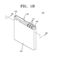
- FIG. 1A is an exploded perspective view illustrating a battery pack, according to an embodiment of the present invention.
- FIG. 1B is a perspective view illustrating a coupled state of the battery pack of FIG. 1A .
- FIG. 1C is a cross-sectional view taken along a line Ic-Ic' of the battery pack of FIG. 1B .
- the battery pack 100 includes a bare cell 110, a protection circuit substrate 120, a cover case 150, and screws 141 and 142.
- the bare cell 110 includes an electrode assembly (not shown) and a sealing assembly 111 accommodating the electrode assembly.
- the electrode assembly may be formed by winding a positive electrode plate (not shown), a negative electrode plate (not shown), and a separator (not shown).
- the sealing assembly 111 includes a cap plate 111 a and a metal type can 111 b and may be formed of a conductive material, for example, aluminum.
- the metal type can 111 b has an open end, and the cap plate 111 a covers the open end of the metal type can 111 b.
- An electrode terminal 114 that is insulated by an insulator 114a is formed in the cap plate 111 a.
- the positive electrode plate of the bare cell 110 is electrically connected to the sealing assembly 111, and the negative electrode plate of the bare cell 110 is electrically connected to the electrode terminal 114.
- the electrode terminal 114 which is connected to the negative electrode plate of the bare cell 110, and the sealing assembly 111, which is connected to the positive electrode plate of the bare cell 110, consequently have different polarities.
- the electrode terminal 114 is electrically connected to the negative electrode plate of the electrode assembly of the bare cell 110 to be a negative electrode P-
- the sealing assembly 111 is electrically connected to the positive electrode plate of the electrode assembly of the bare cell 110 to be a positive electrode P+, but the present invention is not limited thereto.
- the bare cell 110 may be a rectangular battery in which the electrode assembly is sealed by the sealing assembly 111 formed of a metal material, and in which any one of the positive electrode plate and the negative electrode plate of the electrode assembly is electrically connected to the sealing assembly 111, and the other plate is connected to the electrode terminal 114.
- the bare cell 110 is a secondary battery.
- the bare cell 110 can be an ion battery or a lithium polymer battery.
- the present invention is not limited thereto.
- the bare cell 110 may be a secondary battery such as a nickel (Ni)-cadmium (Cd) battery, a Ni-metal hydride (MH) battery, or the like.
- One surface of the cap plate 111a of the bare cell 110 includes a pair of blind bores 112 and 113.
- a first blind bore 112 is coupled with the first screw 141
- the second blind bore 113 is coupled with the second screw 142.
- a screw thread is formed in each of inner circumferential surfaces of the first and second blind bores 112 and 113 in order for the first and second screws 141 and 142 to be coupled therewith.
- the cap plate 111 a comprises a protruding part P corresponding to each of the blind bores 112 and 113.
- the protection circuit substrate 120 includes an insulating substrate 121, a printed circuit pattern (not shown), a conductive pad 123, a protection circuit unit 124, a charging/discharging terminal 125, and first and second tabs 131 and 132.
- the conductive pad 123, the protection circuit unit 124, and the charging/discharging terminal 125 are soldered to the printed circuit pattern formed on the insulating substrate 121.
- the protection circuit substrate 120 is electrically connected to the bare cell 110.
- a negative electrode of the protection circuit substrate 120 is electrically connected to the electrode terminal 114, which is the negative electrode P- of the bare cell 110, by a lead tab 120a, and a positive electrode of the protection circuit substrate 120 is electrically connected to the sealing assembly 110, which is the positive electrode P+ of the bare cell 110, by the first tab 131.
- a positive temperature coefficient (PTC) device 120a1 is electrically connected between the negative electrode of the protection circuit substrate 120 and the electrode terminal 114 and serves to block the electrical connection between the negative electrode of the protection circuit substrate 120 and the electrode terminal 114 when the temperature thereof is excessively high or an excessive current flows therethrough.
- the protection circuit unit 124 may comprise a passive device such as a resistor, a capacitor, or the like, an active device such as a field-effect transistor, a safety device such as the PTC device 120a1, and integrated circuits.
- the protection circuit unit 124 charges or discharges the bare cell 110 when the bare cell 110 is to be charged/discharged, and blocks a charging/discharging path in the bare cell 110 when the bare cell 110 is overheated or is in an overcurrent state, thereby preventing the bare cell 110 from lifetime degradation, overheating, exploding, and the like.
- the first and second tabs 131 and 132 are respectively formed on different ends of the protection circuit substrate 120 to electrically connect the protection circuit substrate 120 and the bare cell 110.
- First and second coupling holes 131 a and 132a are formed in the first and second tabs 131 and 132 corresponding to the blind bores 112 and 113, respectively.
- the first tab 131 and the second tab 132 are connected to the cap plate 111a of the bare cell 110.
- the first and second coupling holes 131 a and 132a respectively corresponding to the first and second blind bores 112 and 113 of the cap plate 111 a are formed in the first tab 131 and the second tab 132.
- the first tab 131 and the second tap 132 support the protection circuit substrate 120 so that the protection circuit substrate 120 is mounted on a surface of the bare cell 110, and electrically connect the positive electrode of the protection circuit module 120 and the positive electrode of the bare cell 110.
- Both the first and second tabs 131 and 132 may be formed of Ni or an alloy containing Ni, and may be soldered to the protection circuit substrate 120.
- the protection circuit substrate 120 is connected to two tabs, that is, the first and second tabs 131 and 132, but the number of tabs is not limited to two.
- the protection circuit substrate 120 may include only the first tab 131.
- the first and second screws 141 and 142 include body parts 141 a and 142a and head parts 141 b and 142b.
- the body parts 141 a and 142a of the first and second screws 141 and 142 include a screw thread that is screw-coupled to the bore 112 and 113 of the bare cell 110.
- the head parts 141 b and 142b of the first and second screws 141 and 142 are formed in an upper part of the body parts 141a and 142a, and have a diameter greater than those of the body parts 141a and 142a.
- grooves marked with + are formed in the head parts 141 b and 142b of the first and second screws 141 and 142 to facilitate rotation.
- the shape of the grooves is not limited thereto. In the present invention, one of ordinary skill in the art may embody the groove having various shapes. In addition to the mark +, the grooves may be marked with ' ⁇ or *.
- a screw driver is inserted into the grooves so that the first and second screws 141 and 142 may be screw-coupled to the bare cell 110.
- the first and second screws 141 and 142 are coupled to the first and second bores 112 and 113b formed on different sides of the bare cell 110, so that the protection circuit substrate 120 may not be twisted and so that the coupling between the first and second tabs 131 and 132 and the protection circuit substrate 120 by soldering is enhanced, thereby preventing an increase in contact resistance.
- the first and second screws 141 and 142 include a conductive material, so that the protection circuit substrate 120 and the bare cell 110 may be electrically connected to each other via the first and second tabs 131 and 132.
- An internal thread may be formed in an inner circumferential surface of the bore 112 to be coupled with the first screw 141.
- the inner circumferential surface of the bore 112 may be formed to be smaller than an outside diameter of the first screw 141 and without an internal thread.
- the first screw 141 serves as a self-tapping screw by cutting a thread into the inner surface of the bore 112 as it is driven into the bore.
- the inner diameter of the bore 112 of the cap plate 111 a may be greater than an inner diameter of the body part 141a and less than an outside diameter of the body part 141 a.
- the cap plate 111 a may include a light alloy, such as aluminum, so as to be easily deformed by the screw thread 141a1 of the first screw 141.
- the second screw 142 and the second blind bore 113 may be similarly configured.
- the cover case 150 includes first and second holes 151a and 152a.
- Mounting grooves 151 b and 152b are formed outside of the first and second holes 151 a and 152a.
- the mounting grooves 151 b and 152b are formed to have inner diameters greater than those of the first and second holes 151a and 152a so as to support head parts 141 b and 142b of the first and second screws 141 and 142.
- the mounting grooves 151 b and 152b will be referred to as a first mounting groove 151 b and a second mounting groove 152b, respectively.
- the first screw 141 is coupled to the first bore 112 formed in the bare cell 110 after passing through the first hole 151 a formed in the cover case 150 and the first coupling hole 131a formed in the first tab 131.
- the head part 141 b of the first screw 141 is tightly adhered to the first mounting groove 151 b of the cover case 150.
- the second screw 142 is coupled in a similar manner. Therefore, the first screw 141 and the second screw 142 couple the cover case 150 to the bare cell 110.
- the cover case 150 is a plastic case made by molding a resin material such as polycarbonate, and protects the protection circuit substrate 120 from an external impact and prevents a short circuit in the protection circuit substrate 120.
- a rib 161 is formed inside the cover case 150, and the rib 161 supports an upper surface of the protection circuit substrate 120 to tightly adhere the protection circuit substrate 120 to the bare cell 110, which prevents the protection circuit substrate 120 from moving, and the contact resistance between the first and second tabs 131 and 132 soldered to the protection circuit substrate 120 and the bare cell 110 from increasing.
- the cover case 150 is coupled with the first and second screws 141 and 142, the first and second tabs 131 and 132 are more tightly adhered to the bare cell 110, so as to prevent an increase in the contact resistance between the first and second taps 131 and 132 and the bare cell 110.
- the contact resistance between the first and second tabs 131 and 132 and the bare cell 110 may be measured through a random free fall (RFF) test.
- the RFF test is performed by dropping six battery packs 100 at the same time from a height of 1 meter two hundred times and measuring contact resistance.
- the structure of the battery pack 100 may be controlled so that variation of the contact resistance obtained by the RFF test is less than a predetermined value.
- the variation of the contact resistance may be controlled to be less than 14 m ⁇ .
- Table 1 shows results of the RFF test performed on the battery pack 100. [Table 1] No.
- the sizes of the bare cell 110 and the case 150 have values within a predetermined range, so that the bare cell 110 and the case 150 may be uniformly mounted on a jig of an engaging device.
- the weight of the battery pack 100 is about 26 g.
- FIG. 3A is an enlarged cross-sectional view of a part llla of FIG. 1C .
- FIG. 3B is a cross-sectional view illustrating a state where a RFF test has been performed on the embodiment of FIG. 3A .
- the first tap 131 and the cap plate 111a are tightly adhered to each other by coupling between the first screw 141 and the cap plate 111 a.
- a gap g is generated between the first tab 131 and the cap plate 111a after the RFF test is performed, and thus contact resistance therebetween is increased.
- Surface precision of the first and second screws 141 and 142 influences the gap g. The surface precision of the first and second screws 141 and 142 may therefore be increased to improve coupling between them and the cap plate and to decrease the rate of contact resistance of the battery pack 100.
- Table 3 shows values of outer diameters (OD) and inner diameters (ID) of an embodiment 4-1 and comparative examples 4-2 and 4-3.
- the outer diameters OD and the inner diameters ID of the first and second screws 141 and 142 are outer diameters and inner diameters of the body parts 141 a of the first and second screws 141 and 142, respectively. That is, a circumscribed circle of a peak of the screw thread 141a1 of the body part 141a is the outer diameter OD, and an inscribed circle of a valley of the screw thread 141a1 is the inner diameter ID.
- a chemical polishing process is performed, and a plating thickness is 5.5 um.
- a chemical polishing process is not performed, and a plating thickness is 2.5 um.
- a chemical polishing process is not performed, and a plating thickness is 4.5 um.
- the error rate of the battery pack 100 is 2,000 ppm (parts-per-million).
- the error rate of the battery pack 100 is 20,000 ppm.
- the difference of the error rate shows that the surface states of the first and second screws 141 and 142 are changed according to whether or not the chemical polishing process has been performed, and thus the surface states of the first and second screws 141 and 142 affect the error rate of the battery pack 100.
- first and second screws 141 and 142 are manufactured, a polishing process is not performed.
- a polishing process is added when the small-sized first and second screws 141 and 142 are manufactured, so as to control surface roughnesses of the first and second screws 141 and 142.
- the small-sized first and second screws 141 and 142 may be screws each having a length of less than 6 mm.
- a raw material for forming the first and second screws 141 and 142 is prepared.
- the raw material may be carbon steel such as SWCH18A.
- the head part 141 b is formed by processing the raw material (S501).
- a screw thread is formed by performing a rolling process (S503).
- a thermal treatment is performed on the first and second screws 141 and 142 through quenching (HV800) and tempering (HV 500 ⁇ 520) processes (S505).
- sizes of the first and second screws 141 and 142 are processed through a chemical polishing process (S507).
- a plating process is performed thereon in order to prevent metal oxidization (S509).
- Table 4 shows values of outer diameters OD and inner diameters ID of the screw through the rolling (S503), chemical polishing process (S507) and plating process (S509).
- the variation of the outer diameters OD of the first and second screws 141 and 142 is greatest during the chemical polishing process. This is because the area of a peak of the screw thread 141a1 is small compared to the inner diameters ID of the first and second screws 141 and 142, and thus the variation of the outer diameter OD decreasing due to the chemical polishing process (S507) is great.
- the variation of the inner diameters ID of the first and second screws 141 and 142 is greatest during the plating process. Since the surface of the body part 141 a is advantageous to deposition of plating during the plating process (S509), the variation of the inner diameter ID may be great during the plating process (S509). Referring to FIG.
- a corner of the screw thread 141 a1 is rounded R in the chemical polishing process, and the surface roughnesses of the first and second screws 141 and 142 become uniform, and thus interference between the surfaces of the screws and the bare cell 110 is reduced, and the screws 141, 142 may be inserted with a relatively small torque. Also, the chemical polishing process reduces variation of the screws 141, 142 thereby reducing the error rate of the battery pack 100.
- the chemical polishing process (S507) will now be described in detail with reference to FIG. 6 .
- a de-greasing process is performed by controlling a composition ratio of caustic soda, surfactant and water to be 1:4:10 (S601).
- an acid treatment is performed on the screws 141 and 142 by controlling a composition ratio of hydrochloric acid, scale remover and water to be 10:1:10 (S603).
- a polishing solution is prepared, wherein a composition ratio of ammonium hydrogen-fluoride, hydrogen peroxide and water in the polishing solution is 1:2:10, and then a polishing process is performed on the screws 141 and 142 (S605).
- each material may have various composition ratios.
- the surface states of the first and second screws 141 and 142 may be changed according to a composition ratio of the ammonium hydrogen-fluoride, hydrogen peroxide and water in the polishing solution of the polishing process (S605), a working environment or a working condition.
- the chemical polishing process (S507) should be performed in consideration of major factors affecting the chemical polishing process (S507).
- the major factors affecting the chemical polishing process (S507) may be controlled so as to process the sizes of the first and second screws 141 and 142 and to control the surface roughnesses thereof. That is, as shown in Table 4, the outer diameters and the inner diameters of the first and second screws 141 and 142 are changed through the chemical polishing process (S507), and the sizes of the first and second screws 141 and 142 may be processed in consideration of factors affecting the variation of the outer diameters and the inner diameters of the first and second screws 141 and 142.
- the factors affecting the chemical polishing process (S507) may be concentration and temperature of the polishing solution used in the chemical polishing process and time for the reaction between the polishing solution and the screws 141 and 142 (S507).
- Table 5 shows a variation of the outer and inner diameters and the surface roughnesses of the first and second screws 141 and 142 according to the concentration of the polishing solution in the chemical polishing process (S507).
- No. Processing Condition Result of Chemical Polishing N Note concentration (hydrometer) temperature (°C) time (s) polishing solution (OD) (mm) inner diameter ID (mm) 1 1 40 10 1.242 0.898 low gloss 2 3 1.241 0.899 low gloss 3 5 1.234 0.895 good 4 7 1.227 0.893 good 5 9 1.233 0.894 good 6 11 1.186 0.874 dimensional error
- the concentration of the polishing solution is 5 through 9
- the sizes and surface roughnesses of the first and second screws 141 and 142 are good.
- the concentration may be measured through a Baume's hydrometer.
- a weight of a material at a predetermined temperature is a unique value of the material. Accordingly, purity of the polishing solution may be checked by measuring the weight. That is, the concentration may be determined by using a relationship between the weight and concentration of the polishing solution.
- the concentration of the polishing solution may vary according to a composition ratio of ammonium hydrogen-fluoride, hydrogen peroxide and water.
- Table 6 Ammonium hydrogen-fluoride (ml) 100 100 100 100 100 100 100 hydrogen peroxide (ml) 50 100 200 250 300 350 Water (ml) 1000 1000 1000 1000 1000 Concentration of a Baum's hydrometer 1 3 5 7 9 11
- Table 7 shows a variation and surface roughnesses of the outer and inner diameters of the first and second screws 141 and 142 according to a temperature of the polishing solution.
- No. Processing Condition Result of Chemical Polishing Note concentration (hydrometer) temperature (oC) time (s) outer diameter OD (mm) inner diameter ID (mm) 1 9 10 10 1.246 0.897 rough 2 20 1.239 0.896 low gloss 3 30 1.235 0.894 good 4 40 1.233 0.894 good 5 50 1.228 0.889 good 6 70 1.222 0.889 lowest limit of size
- the first and second screws 141 and 142 had preferable sizes and surface roughnesses. That is, the sizes and surface roughnesses of the first and second screws 141 and 142 may be controlled by controlling the temperature of the polishing solution during the chemical polishing process (S507).
- Table 8 shows a variation of outer and inner diameters and surface roughnesses of the first and second screws 141 and 142 according to time.
- No. Processing Condition Result of Chemical Polishing Note concentration (hydrometer) temperature (°C) time (s) outer diameter OD (mm) inner diameter ID (mm) 1 9 40 5 1.244 0.896 inner diameter is rough good 2 10 1.233 0.894 3 15 1.226 0.890 good 4 20 1.209 0.886 lowest limit of size 5 30 1.183 0.876 poor size 6 40 1.159 0.868 poor size
- the first and second screws 141 and 142 had preferable sizes and surface roughnesses. Also, values of the sizes and surface roughnesses of the first and second screws 141 and 142 may be obtained by satisfying the concentration and temperature of the polishing solution and time for the reaction between the polishing solution and the screws 141 and 142.
- a condition in which the concentration is 5 through 9, the temperature is 30°C through 50°C, and the time for the reaction between the polishing solution and the screws 141 and 142 is 10 s through 15 s, is defined as a first condition.
- the outer diameters OD of the first and second screws 141 and 142 having undergone the chemical polishing process (S507) according to the first condition may be 1.22 mm through 1.27 mm, and the inner diameter ID thereof may be 0.88 mm through 0.93 mm.
- the outer diameter OD may be 1.226 mm through 1.235 mm, and the inner diameter ID may be 0.889 mm through 0.895 mm.
- the present invention is not limited thereto.
- the concentration and temperature of the polishing solution and time for the reaction between the polishing solution and the screws 141 and 142 may affect the sizes and surface roughnesses of the first and second screws 141 and 142
- the first and second screws 141 and 142 may be manufactured by controlling the concentration and temperature of the polishing solution and time for the reaction between the polishing solution .and_the screws 141 and 142.
- Coupling and a coupling error rate of the first and second screws 141 and 142 coupled with a light alloy metal are significantly different according to surface precision of the first and second screws 141 and 142. That is, minute burs, external substances, etc. generated during the manufacturing process of the first and second screws 141 and 142 undergo the chemical polishing process (S507), and thus the shape of the screw threads 141a1 of the first and second screws 141 and 142 are rounded and the surfaces of the screw threads 141a1 are smoothened. Accordingly, frictional resistance generated when the first and second screws 141 and 142 are coupled with the light alloy metal and damage applied to the light alloy metal are minimized, thereby improving coupling of the first and second screws 141 and 142.
- the first and second screws 141 and 142 having undergone the chemical polishing process (S507) according to the first condition may have clamping force of about 180 N when being coupled with the first and second bores 112 and 113.
- Table 9 shows a result of the RFF test performed on the battery pack 100 using the first and second screws 141 and 142 whose sizes are processed through the chemical polishing process (S507), under the first condition.
- No. Initial (m ⁇ ) 50 times (m ⁇ ) 100 times (m ⁇ ) 150 times (m ⁇ ) 200 times (m ⁇ )
- Note 1 132.3 132.4 131.5 136.5 134.1 good 2 130.1 131.7 138.5 139.7 139.3 good 3 130.3 133.1 132.3 133.2 135.1 good 4 130.2 132.2 136.6 137.1 136.2 good 5 131.2 134.4 133.2 135.1 138.2 good 6 131.5 132.6 133.3 136.8 136.5 good
- the battery pack 100 has a coupling error rate of less than about 1,000 ppm during a coupling process, and thus process stability has been improved.
- a suitable mechanical polishing operation may be single stage process or a multi stage process.
- a multi stage process a succession of progressively finer abrasives would normally be used.
- polishing lubricants may be used to assist the polishing process.
Abstract
A battery assembly comprising: a bare cell; a protection circuit substrate, upon which protection circuit components are mounted; at least one connection tab, connecting the protection circuit substrate to the bare cell; and a case, in which the protection circuit substrate is housed; wherein the connection tab is connected to the bare cell via a screw and the screw has been polished.
Description
- The present invention relates to a battery pack and a method of manufacturing the same.
- Portable electrical and electronic devices typically include battery packs that enable them to be operated in places where additional power sources are not available. Such, battery packs frequently employ economical secondary batteries that are capable of charging and discharging. Representative secondary batteries include a nickel (Ni)-cadmium (Cd) battery, a Ni-MH battery, a lithium (Li) battery and a Li-ion secondary battery.
- A secondary battery is typically formed of a bare cell formed by sealing a can accommodating an electrode assembly and an electrolyte, and a protection circuit substrate electrically connected to the bare cell. The bare cell charges/discharges electricity via a chemical reaction. The protection circuit substrate controls charging/discharging of the bare cell and prevents overcharging/overdischarging of the bare cell to protect the bare cell. When the bare cell and the protection circuit are connected to form the secondary battery, if the electrical resistance between the bare cell and the protection circuit module is great, the charging/discharging efficiency of the bare cell is compromised.
- If there is an external impact to the secondary battery the contact resistance can increase in a region where the bare cell and the protection circuit substrate are connected, due to the impact disrupting the contact between the two. This will in turn have a negative impact upon the charging/discharging efficiency of the bare cell. In view of this, the secondary battery may go through a reliability test for determining whether the secondary battery is stable enough to withstand an impact caused when mounting the secondary battery in an electronic product.
- The present invention seeks out to provide a battery assembly that offers greater resistance to impact, thereby avoiding a reduction in charging/discharging efficiency.
- Accordingly, a first aspect of the invention provides a battery assembly as set out in Claim 1.
- An embodiment of the present invention therefore enables the coupling between a bare cell and a case to be enhanced, and thus the likelihood of an increase in electrical resistance between the bare cell and a protection circuit substrate due to an external impact can be reduced.
- Preferred features of this aspect of the invention are set out in claims 2 to 8.
- A further aspect of the invention provides a method of manufacturing a screw for connecting a connection tab to a bare cell in a battery assembly as set out in Claim 9. Preferred features of this aspect of the invention are set out in Claims 10 to 15.
- Embodiments of the invention will be described below by way of example and with reference to the accompanying drawings, in which:-
-
FIG. 1A is an exploded perspective view illustrating a battery pack, according to an embodiment of the present invention; -
FIG. 1B is a perspective view illustrating a coupled state of the battery pack ofFIG. 1A ; -
FIG. 1C is a cross-sectional view taken along a line Ic-Ic' ofFIG. 1B ; -
FIG. 2 is a schematic exploded perspective view illustrating sizes of portions of a battery pack, according to an embodiment of the present invention; -
FIG. 3A is an enlarged cross-sectional view of a part llla ofFIG. 1C ; -
FIG. 3B is a cross-sectional view illustrating a state where a random free fall (RFF) test has been performed on the embodiment ofFIG. 3A ; -
FIG. 4 is a schematic cross-sectional view illustrating a screw, according to an embodiment of the present invention; -
FIG. 5 is a flowchart of a method of manufacturing a screw, according to an embodiment of the present invention; and -
FIG. 6 is a flowchart of a chemical polishing process. - Reference will now be made in detail to embodiments of the invention, examples of which are illustrated in the accompanying drawings.
- According to a first embodiment of the present invention, a
battery pack 100 includesscrews bare cell 110 and acase 150. Hereinafter, thebattery pack 100 will be described with reference toFIGS. 1A through 1C and2 , and thescrews FIGS. 3 through 6 . -
FIG. 1A is an exploded perspective view illustrating a battery pack, according to an embodiment of the present invention.FIG. 1B is a perspective view illustrating a coupled state of the battery pack ofFIG. 1A .FIG. 1C is a cross-sectional view taken along a line Ic-Ic' of the battery pack ofFIG. 1B . As illustrated inFIGS. 1A through 1D , thebattery pack 100 includes abare cell 110, aprotection circuit substrate 120, acover case 150, andscrews - The
bare cell 110 includes an electrode assembly (not shown) and asealing assembly 111 accommodating the electrode assembly. The electrode assembly may be formed by winding a positive electrode plate (not shown), a negative electrode plate (not shown), and a separator (not shown). Thesealing assembly 111 includes acap plate 111 a and a metal type can 111 b and may be formed of a conductive material, for example, aluminum. The metal type can 111 b has an open end, and thecap plate 111 a covers the open end of the metal type can 111 b. Anelectrode terminal 114 that is insulated by aninsulator 114a is formed in thecap plate 111 a. - The positive electrode plate of the
bare cell 110 is electrically connected to thesealing assembly 111, and the negative electrode plate of thebare cell 110 is electrically connected to theelectrode terminal 114. Theelectrode terminal 114, which is connected to the negative electrode plate of thebare cell 110, and thesealing assembly 111, which is connected to the positive electrode plate of thebare cell 110, consequently have different polarities. In the current embodiment, theelectrode terminal 114 is electrically connected to the negative electrode plate of the electrode assembly of thebare cell 110 to be a negative electrode P-, and thesealing assembly 111 is electrically connected to the positive electrode plate of the electrode assembly of thebare cell 110 to be a positive electrode P+, but the present invention is not limited thereto. In other words, thebare cell 110 may be a rectangular battery in which the electrode assembly is sealed by thesealing assembly 111 formed of a metal material, and in which any one of the positive electrode plate and the negative electrode plate of the electrode assembly is electrically connected to thesealing assembly 111, and the other plate is connected to theelectrode terminal 114. Here, thebare cell 110 is a secondary battery. In practice, this means that thebare cell 110 can be an ion battery or a lithium polymer battery. However, the present invention is not limited thereto. Thus, thebare cell 110 may be a secondary battery such as a nickel (Ni)-cadmium (Cd) battery, a Ni-metal hydride (MH) battery, or the like. - One surface of the
cap plate 111a of thebare cell 110 includes a pair ofblind bores blind bore 112 is coupled with thefirst screw 141, and the secondblind bore 113 is coupled with thesecond screw 142. A screw thread is formed in each of inner circumferential surfaces of the first and second blind bores 112 and 113 in order for the first andsecond screws cap plate 111 a comprises a protruding part P corresponding to each of the blind bores 112 and 113. - The
protection circuit substrate 120 includes an insulatingsubstrate 121, a printed circuit pattern (not shown), aconductive pad 123, aprotection circuit unit 124, a charging/dischargingterminal 125, and first andsecond tabs conductive pad 123, theprotection circuit unit 124, and the charging/dischargingterminal 125 are soldered to the printed circuit pattern formed on the insulatingsubstrate 121. Theprotection circuit substrate 120 is electrically connected to thebare cell 110. That is, a negative electrode of theprotection circuit substrate 120 is electrically connected to theelectrode terminal 114, which is the negative electrode P- of thebare cell 110, by alead tab 120a, and a positive electrode of theprotection circuit substrate 120 is electrically connected to the sealingassembly 110, which is the positive electrode P+ of thebare cell 110, by thefirst tab 131. A positive temperature coefficient (PTC) device 120a1 is electrically connected between the negative electrode of theprotection circuit substrate 120 and theelectrode terminal 114 and serves to block the electrical connection between the negative electrode of theprotection circuit substrate 120 and theelectrode terminal 114 when the temperature thereof is excessively high or an excessive current flows therethrough. Theprotection circuit unit 124 may comprise a passive device such as a resistor, a capacitor, or the like, an active device such as a field-effect transistor, a safety device such as the PTC device 120a1, and integrated circuits. Theprotection circuit unit 124 charges or discharges thebare cell 110 when thebare cell 110 is to be charged/discharged, and blocks a charging/discharging path in thebare cell 110 when thebare cell 110 is overheated or is in an overcurrent state, thereby preventing thebare cell 110 from lifetime degradation, overheating, exploding, and the like. - The first and
second tabs protection circuit substrate 120 to electrically connect theprotection circuit substrate 120 and thebare cell 110. First and second coupling holes 131 a and 132a are formed in the first andsecond tabs FIG. 1C , thefirst tab 131 and thesecond tab 132 are connected to thecap plate 111a of thebare cell 110. The first and second coupling holes 131 a and 132a respectively corresponding to the first and second blind bores 112 and 113 of thecap plate 111 a are formed in thefirst tab 131 and thesecond tab 132. Thefirst tab 131 and thesecond tap 132 support theprotection circuit substrate 120 so that theprotection circuit substrate 120 is mounted on a surface of thebare cell 110, and electrically connect the positive electrode of theprotection circuit module 120 and the positive electrode of thebare cell 110. - Both the first and
second tabs protection circuit substrate 120. In this case, inFIG. 1A , theprotection circuit substrate 120 is connected to two tabs, that is, the first andsecond tabs protection circuit substrate 120 may include only thefirst tab 131. - The first and
second screws body parts head parts body parts second screws bore bare cell 110. Thehead parts second screws body parts body parts FIG. 1A , grooves marked with + are formed in thehead parts second screws second screws bare cell 110. The first andsecond screws second bores 112 and 113b formed on different sides of thebare cell 110, so that theprotection circuit substrate 120 may not be twisted and so that the coupling between the first andsecond tabs protection circuit substrate 120 by soldering is enhanced, thereby preventing an increase in contact resistance. Also, the first andsecond screws protection circuit substrate 120 and thebare cell 110 may be electrically connected to each other via the first andsecond tabs - An internal thread may be formed in an inner circumferential surface of the
bore 112 to be coupled with thefirst screw 141. Alternatively, the inner circumferential surface of thebore 112 may be formed to be smaller than an outside diameter of thefirst screw 141 and without an internal thread. In such a case thefirst screw 141 serves as a self-tapping screw by cutting a thread into the inner surface of thebore 112 as it is driven into the bore. For example, the inner diameter of thebore 112 of thecap plate 111 a may be greater than an inner diameter of thebody part 141a and less than an outside diameter of thebody part 141 a. Therefore, when thebore 112 is coupled to thefirst screw 141, the inner circumferential surface of thescrew receiving groove 112 is deformed to be tightly adhered to thebody part 141a of thefirst screw 141. Thecap plate 111 a may include a light alloy, such as aluminum, so as to be easily deformed by the screw thread 141a1 of thefirst screw 141. - The
second screw 142 and the secondblind bore 113 may be similarly configured. - The
cover case 150 includes first andsecond holes grooves second holes grooves second holes head parts second screws grooves groove 151 b and asecond mounting groove 152b, respectively. Thefirst screw 141 is coupled to thefirst bore 112 formed in thebare cell 110 after passing through thefirst hole 151 a formed in thecover case 150 and thefirst coupling hole 131a formed in thefirst tab 131. Thehead part 141 b of thefirst screw 141 is tightly adhered to the first mountinggroove 151 b of thecover case 150. Thesecond screw 142 is coupled in a similar manner. Therefore, thefirst screw 141 and thesecond screw 142 couple thecover case 150 to thebare cell 110. Thecover case 150 is a plastic case made by molding a resin material such as polycarbonate, and protects theprotection circuit substrate 120 from an external impact and prevents a short circuit in theprotection circuit substrate 120. - Referring to
FIG. 1C , arib 161 is formed inside thecover case 150, and therib 161 supports an upper surface of theprotection circuit substrate 120 to tightly adhere theprotection circuit substrate 120 to thebare cell 110, which prevents theprotection circuit substrate 120 from moving, and the contact resistance between the first andsecond tabs protection circuit substrate 120 and thebare cell 110 from increasing. When thecover case 150 is coupled with the first andsecond screws second tabs bare cell 110, so as to prevent an increase in the contact resistance between the first andsecond taps bare cell 110. - The contact resistance between the first and
second tabs bare cell 110 may be measured through a random free fall (RFF) test. The RFF test is performed by dropping sixbattery packs 100 at the same time from a height of 1 meter two hundred times and measuring contact resistance. In this case, the structure of thebattery pack 100 may be controlled so that variation of the contact resistance obtained by the RFF test is less than a predetermined value. The variation of the contact resistance may be controlled to be less than 14 mΩ. Table 1 shows results of the RFF test performed on thebattery pack 100.[Table 1] No. Initial Value (mΩ) 50 times (mΩ) 100 times (mΩ) 150 times (mΩ) 200 times (mΩ) Result 1 134.5 137.4 141.5 146.5 144.3 good 2 131.5 135.7 138.7 139.2 139.4 good 3 135.5 137.1 142.4 143.5 180.0 poor 4 131.7 139.2 156.0 147.1 146.7 poor 5 135.0 138.4 153.0 149.0 158.0 poor 6 134.2 145.6 183.0 156.0 156.5 poor - As shown in Table 1, contact resistances of four
battery packs 100, from among the sixbattery packs 100, were poor. The sizes of the battery packs 100 used in the RFF test will be described with reference to Table 2. The sizes of the battery packs 100 used in Table 2 will be described with reference toFIG. 2 . Here, W1 and W2, H1 and T1 denote widths, a height and a thickness of thebare cell 110, respectively. W3 and W4, H2 and T2 denote widths, a height and a thickness of thecase 150, respectively.[Table 2] Bare Cell 110Case 150No. W1 (mm) W2(mm) H1 (mm) T1 (mm) W3(mm) W4(mm) H2(mm) T2(mm) 1 43.81 40.40 41.86 5.16 44.11 40.38 4.68 5.75 2 43.79 40.40 41.85 5.17 44.10 40.39 4.69 5.76 3 43.79 40.39 41.84 5.16 44.09 40.39 4.67 5.76 4 43.79 40.40 41.85 5.17 44.10 40.40 4.69 5.76 5 43.80 40.40 41.83 5.16 44.10 40.39 4.71 5.76 6 43.81 40.40 41.85 5.17 44.10 40.38 4.68 5.75 MIN 43.79 40.39 41.83 5.16 44.09 40.38 4.67 5.75 MAX 43.81 40.40 41.86 5.17 44.11 40.40 4.71 5.76 difference 0.02 0.01 0.03 0.01 0.02 0.016 0.04 0.01 - Here, the sizes of the
bare cell 110 and thecase 150 have values within a predetermined range, so that thebare cell 110 and thecase 150 may be uniformly mounted on a jig of an engaging device. In this case, the weight of thebattery pack 100 is about 26 g. - The state of coupling between the
first tab 131 and thecap plate 111a before and after performing the RFF test will be described with reference toFIGS. 3A and 3B. FIG. 3A is an enlarged cross-sectional view of a part llla ofFIG. 1C .FIG. 3B is a cross-sectional view illustrating a state where a RFF test has been performed on the embodiment ofFIG. 3A . InFIG. 3A , thefirst tap 131 and thecap plate 111a are tightly adhered to each other by coupling between thefirst screw 141 and thecap plate 111 a. A gap g is generated between thefirst tab 131 and thecap plate 111a after the RFF test is performed, and thus contact resistance therebetween is increased. Surface precision of the first andsecond screws second screws battery pack 100. - Table 3 shows values of outer diameters (OD) and inner diameters (ID) of an embodiment 4-1 and comparative examples 4-2 and 4-3. Referring to
FIG. 4 , the outer diameters OD and the inner diameters ID of the first andsecond screws body parts 141 a of the first andsecond screws body part 141a is the outer diameter OD, and an inscribed circle of a valley of the screw thread 141a1 is the inner diameter ID.[Table 3] No. Embodiment 4-1 Comparative Example 4-2 Comparative Example 4-3 outer diameter 1 (mm) inner diameter 1 (mm) outer diameter 2 (mm) inner diameter 2 (mm) outer diameter 3 (mm) inner diameter 3 (mm) 1 1.212 0.875 1.217 0.869 1.211 0.869 2 1.216 0.867 1.215 0.858 1.213 0.873 3 1.209 0.872 1.212 0.877 1.219 0.873 4 1.205 0.872 1.216 0.862 1.210 0.868 5 1.210 0.870 1.217 0.874 1.200 0.874 6 1.205 0.871 1.215 0.876 1.206 0.880 Max 1.216 0.875 1.217 0.877 1.219 0.880 Min 1.205 0.867 1.212 0.858 1.200 0.868 Ave 1.210 0.871 1.215 0.869 1.210 0.873 Range 0.011 0.008 0.005 0.019 0.019 0.012 Chemical Polishing yes no no Plating Thickness (um) 5.5 2.5 4.5 - Referring to Table 3, in the embodiment 4-1, a chemical polishing process is performed, and a plating thickness is 5.5 um. In the comparative example 4-2, a chemical polishing process is not performed, and a plating thickness is 2.5 um. In the comparative example 4-3, a chemical polishing process is not performed, and a plating thickness is 4.5 um. When the
battery pack 100 is configured as an embodiment 4-1, the error rate of thebattery pack 100 is 2,000 ppm (parts-per-million). On the other hand, when the battery pack is configured as in comparative examples 4-2 and 4-3, the error rate of thebattery pack 100 is 20,000 ppm. The difference of the error rate shows that the surface states of the first andsecond screws second screws battery pack 100. - In general, when small-sized first and
second screws second screws second screws second screws - A method of manufacturing the small-sized first and
second screws FIG. 5 . - First, a raw material for forming the first and
second screws head part 141 b is formed by processing the raw material (S501). A screw thread is formed by performing a rolling process (S503). A thermal treatment is performed on the first andsecond screws second screws - Table 4 shows values of outer diameters OD and inner diameters ID of the screw through the rolling (S503), chemical polishing process (S507) and plating process (S509).
[Table 4] No. Outer Diameter OD of Screw Inner Diameter ID of Screw rolling (mm) chemical polishing (mm) plating (mm) rolling (mm) chemical polishing (mm) plating (mm) 1 1.269 1.250 1.255 0.908 0.900 0.913 2 1.257 1.239 1.250 0.903 0.896 0.916 3 1.255 1.237 1.250 0.901 0.895 0.918 - Referring to Table 4, the variation of the outer diameters OD of the first and
second screws second screws second screws body part 141 a is advantageous to deposition of plating during the plating process (S509), the variation of the inner diameter ID may be great during the plating process (S509). Referring toFIG. 4 , a corner of thescrew thread 141 a1 is rounded R in the chemical polishing process, and the surface roughnesses of the first andsecond screws bare cell 110 is reduced, and thescrews screws battery pack 100. - The chemical polishing process (S507) will now be described in detail with reference to
FIG. 6 . After the thermal treatment (S505) is performed, a de-greasing process is performed by controlling a composition ratio of caustic soda, surfactant and water to be 1:4:10 (S601). Then, an acid treatment is performed on thescrews screws 141 and 142 (S605). Then, hydrochloric acid and water are activated with a composition ratio of 1:2 (S607), and a neutralization treatment is performed on thescrews screws 141 and 142 (S601), thereby completing the chemical polishing process (S507). The chemical polishing process ofFIG. 6 is just an embodiment, and each material may have various composition ratios. The surface states of the first andsecond screws second screws second screws - According to the chemical polishing process (S507) of the present invention, the major factors affecting the chemical polishing process (S507) may be controlled so as to process the sizes of the first and
second screws second screws second screws second screws screws 141 and 142 (S507). - Table 5 shows a variation of the outer and inner diameters and the surface roughnesses of the first and
second screws [Table 5] No. Processing Condition Result of Chemical Polishing N Note concentration (hydrometer) temperature (°C) time (s) polishing solution (OD) (mm) inner diameter ID (mm) 1 1 40 10 1.242 0.898 low gloss 2 3 1.241 0.899 low gloss 3 5 1.234 0.895 good 4 7 1.227 0.893 good 5 9 1.233 0.894 good 6 11 1.186 0.874 dimensional error - When the concentration of the polishing solution is 5 through 9, the sizes and surface roughnesses of the first and
second screws - Referring table 6, the concentration of the polishing solution may vary according to a composition ratio of ammonium hydrogen-fluoride, hydrogen peroxide and water.
Table 6 Ammonium hydrogen-fluoride (ml) 100 100 100 100 100 100 hydrogen peroxide (ml) 50 100 200 250 300 350 Water (ml) 1000 1000 1000 1000 1000 1000 Concentration of a Baum's hydrometer 1 3 5 7 9 11 - Table 7 shows a variation and surface roughnesses of the outer and inner diameters of the first and
second screws [Table 7] No. Processing Condition Result of Chemical Polishing Note concentration (hydrometer) temperature (ºC) time (s) outer diameter OD (mm) inner diameter ID (mm) 1 9 10 10 1.246 0.897 rough 2 20 1.239 0.896 low gloss 3 30 1.235 0.894 good 4 40 1.233 0.894 good 5 50 1.228 0.889 good 6 70 1.222 0.889 lowest limit of size - When a temperature of the polishing solution is 30°C through 50°C, the first and
second screws second screws - Table 8 shows a variation of outer and inner diameters and surface roughnesses of the first and
second screws [Table 8] No. Processing Condition Result of Chemical Polishing Note concentration (hydrometer) temperature (°C) time (s) outer diameter OD (mm) inner diameter ID (mm) 1 9 40 5 1.244 0.896 inner diameter is rough good 2 10 1.233 0.894 3 15 1.226 0.890 good 4 20 1.209 0.886 lowest limit of size 5 30 1.183 0.876 poor size 6 40 1.159 0.868 poor size - Referring to Table 8, when time is 10 s through 15 s, the first and
second screws - Accordingly, referring to Tables 5 through 8, when the concentration is 5 through 9, when the temperature of the polishing solution is 30°C through 50°C, and when the time for the reaction between the polishing solution and_the screws 141 and 142 is 10 s through 15 s, the first and
second screws second screws screws - Now, a condition, in which the concentration is 5 through 9, the temperature is 30°C through 50°C, and the time for the reaction between the polishing solution and the
screws second screws screws second screws second screws - Coupling and a coupling error rate of the first and
second screws second screws second screws second screws second screws second screws second screws second bores - Table 9 shows a result of the RFF test performed on the
battery pack 100 using the first andsecond screws [Table 9] No. Initial (mΩ) 50 times (mΩ) 100 times (mΩ) 150 times (mΩ) 200 times (mΩ) Note 1 132.3 132.4 131.5 136.5 134.1 good 2 130.1 131.7 138.5 139.7 139.3 good 3 130.3 133.1 132.3 133.2 135.1 good 4 130.2 132.2 136.6 137.1 136.2 good 5 131.2 134.4 133.2 135.1 138.2 good 6 131.5 132.6 133.3 136.8 136.5 good - Compared to the result of Table 1, the results of Table 9 are significantly improved.
- Also, the
battery pack 100 has a coupling error rate of less than about 1,000 ppm during a coupling process, and thus process stability has been improved. - Although the above processes make use of chemical polishing, mechanical polishing and buffing techniques are also applicable to the invention.
- A suitable mechanical polishing operation may be single stage process or a multi stage process. In a multi stage process, a succession of progressively finer abrasives would normally be used. As is conventional, polishing lubricants may be used to assist the polishing process.
- It should be understood that the embodiments described herein should be considered in a descriptive sense only and not for purposes of limitation. Descriptions of features or aspects within each embodiment should typically be considered as available for other similar features or aspects in other embodiments.
Claims (15)
- A battery assembly comprising:a bare cell;a protection circuit substrate, upon which protection circuit components are mounted;at least one connection tab, connecting the protection circuit substrate to the bare cell; anda case, in which the protection circuit substrate is housed;wherein the connection tab is connected to the bare cell via a screw and
the screw has been polished. - A battery assembly according to Claim 1, wherein the screw has been chemically polished.
- A battery assembly according to any preceding claim, wherein the screw extends through an opening in the connection tab.
- A battery assembly according to any preceding claim, wherein the screw extends into a bore provided in the bare cell.
- A battery assembly according to Claim 4 wherein the bore is a blind bore and there is a gap between an end of the bore and a tip portion of the screw.
- A battery assembly according to any preceding claim, wherein the screw also connects the case to the bare cell and the case comprises an opening through which the screw extends towards the bare cell.
- A battery assembly according to any preceding claim, wherein the screw is a self-tapping screw.
- A battery assembly according to any preceding claim, comprising two connection tabs and two screws, each said screw connecting a respective one of the said connecting tabs to the bare cell.
- A method of manufacturing a screw for connecting a connection tab to a bare cell in a battery assembly, the said method comprising:forming a screw head;forming a thread portion; andsubjecting the screw to a polishing process;wherein the size of the screw is controlled by the polishing process.
- A method according to Claim 9, wherein the polishing process is a chemical polishing process involving the application of a polishing solution.
- A method according to Claim 9 or 10, wherein the chemical polishing process comprises:a de-greasing stepan acid treatment;application of the polishing solution;an acid and water activation treatment;a neutralisation treatment;a dehydration treatment; anda drying step.
- A method according to Claim 12, wherein the concentration of the polishing solution is from 5 to 9 when measured using a Baume's hydrometer: the polishing solution has a temperature of from 30 to 50 °C; and/or the polishing solution is applied for a period of from 10 to 15 seconds.
- A method according to one of Claims 8 to 12, wherein the length of the screw is controlled to be 6mm or less.
- A method according to one of Claims 8 to 13, wherein the outer diameter of the thread is controlled to be from 1.22mm to 1.27mm and/or the inner diameter of the thread is controlled to be from 0.88mm to 0.93mm.
- A method according to one of Claims 8 to 14, wherein at least one dimension of the screw is controlled to provide a predetermined resistance to separation between a tab and a bare cell of a battery assembly.
Applications Claiming Priority (2)
| Application Number | Priority Date | Filing Date | Title |
|---|---|---|---|
| US31019310P | 2010-03-03 | 2010-03-03 | |
| US12/975,237 US20110217571A1 (en) | 2010-03-03 | 2010-12-21 | Battery pack and method of manufacturing same |
Publications (1)
| Publication Number | Publication Date |
|---|---|
| EP2365558A1 true EP2365558A1 (en) | 2011-09-14 |
Family
ID=44149826
Family Applications (1)
| Application Number | Title | Priority Date | Filing Date |
|---|---|---|---|
| EP20110250026 Withdrawn EP2365558A1 (en) | 2010-03-03 | 2011-01-12 | Battery pack and method of manufacturing same |
Country Status (5)
| Country | Link |
|---|---|
| US (1) | US20110217571A1 (en) |
| EP (1) | EP2365558A1 (en) |
| JP (1) | JP5647034B2 (en) |
| KR (1) | KR101234238B1 (en) |
| CN (1) | CN102195069A (en) |
Cited By (2)
| Publication number | Priority date | Publication date | Assignee | Title |
|---|---|---|---|---|
| EP2706588A1 (en) * | 2012-09-11 | 2014-03-12 | Samsung SDI Co., Ltd. | Lead tab, battery pack having the lead tab and method of manufacturing the lead tab |
| DE102014225064A1 (en) | 2014-12-05 | 2016-06-09 | Robert Bosch Gmbh | A storage device for storing electrical energy with apparatus for passing signals through an outer wall of the storage device |
Families Citing this family (2)
| Publication number | Priority date | Publication date | Assignee | Title |
|---|---|---|---|---|
| KR101381680B1 (en) * | 2011-10-31 | 2014-04-04 | 주식회사 엘지화학 | Battery Pack Comprising Charging Coil |
| KR102019472B1 (en) * | 2015-10-05 | 2019-09-06 | 주식회사 엘지화학 | Battery module and battery pack including the same |
Citations (5)
| Publication number | Priority date | Publication date | Assignee | Title |
|---|---|---|---|---|
| JPS5656747A (en) * | 1979-10-15 | 1981-05-18 | Seiko Instr & Electronics Ltd | Thread rolling tool |
| JP2000158077A (en) * | 1998-11-20 | 2000-06-13 | Nec Ibaraki Ltd | Screw forging method, and thread rolling tool therefor |
| US20040251872A1 (en) * | 2003-06-13 | 2004-12-16 | Chuanfu Wang | Lithium ion batteries |
| EP1814189A1 (en) * | 2004-10-27 | 2007-08-01 | Matsushita Electric Industrial Co., Ltd. | Battery pack |
| EP2071648A1 (en) * | 2007-12-14 | 2009-06-17 | Samsung SDI Co., Ltd. | Battery pack |
Family Cites Families (12)
| Publication number | Priority date | Publication date | Assignee | Title |
|---|---|---|---|---|
| JP3144280B2 (en) * | 1995-08-25 | 2001-03-12 | 住友金属工業株式会社 | Pretreatment method for iron-based metal materials for etching |
| JP2001342584A (en) * | 2000-05-31 | 2001-12-14 | Nitto Seiko Co Ltd | Stain removal process in manufacturing screw |
| JP2003004116A (en) * | 2001-06-25 | 2003-01-08 | Dyadic Systems Co Ltd | Long-life sliding screw mechanism and electric rotation/ linear motion conversion mechanism |
| CN1218797C (en) * | 2001-06-29 | 2005-09-14 | 宣碧华 | Method for manufacturing chain |
| JP4240523B2 (en) * | 2001-09-21 | 2009-03-18 | 富士フイルム株式会社 | Battery connection terminal |
| CN1259743C (en) * | 2002-09-16 | 2006-06-14 | 华南师范大学 | Surface treatment method for positive current collector of alkaline zinc-manganese battery with inner surface provided with cog structure |
| US20050013680A1 (en) * | 2003-07-18 | 2005-01-20 | Steve Karaga | Screws and methods of driving a screw into a workpiece |
| JP4568091B2 (en) * | 2004-11-16 | 2010-10-27 | 三洋電機株式会社 | Pack battery |
| EP1712659A1 (en) * | 2005-04-11 | 2006-10-18 | Elisha Holding LLC | Corrosion resistant article and method of production thereof |
| KR100889210B1 (en) * | 2007-05-28 | 2009-03-16 | 문병원 | Hot-dip galvanizing method for fastener |
| JP2009176631A (en) * | 2008-01-25 | 2009-08-06 | Fdk Energy Co Ltd | Alkaline battery current collection rod, and alkaline battery |
| JP2009211840A (en) * | 2008-02-29 | 2009-09-17 | Seiko Instruments Inc | Method for manufacturing alkaline battery and alkaline battery |
-
2010
- 2010-12-21 US US12/975,237 patent/US20110217571A1/en not_active Abandoned
-
2011
- 2011-01-05 KR KR1020110001085A patent/KR101234238B1/en active IP Right Grant
- 2011-01-12 EP EP20110250026 patent/EP2365558A1/en not_active Withdrawn
- 2011-02-21 CN CN2011100430059A patent/CN102195069A/en active Pending
- 2011-03-03 JP JP2011046345A patent/JP5647034B2/en active Active
Patent Citations (5)
| Publication number | Priority date | Publication date | Assignee | Title |
|---|---|---|---|---|
| JPS5656747A (en) * | 1979-10-15 | 1981-05-18 | Seiko Instr & Electronics Ltd | Thread rolling tool |
| JP2000158077A (en) * | 1998-11-20 | 2000-06-13 | Nec Ibaraki Ltd | Screw forging method, and thread rolling tool therefor |
| US20040251872A1 (en) * | 2003-06-13 | 2004-12-16 | Chuanfu Wang | Lithium ion batteries |
| EP1814189A1 (en) * | 2004-10-27 | 2007-08-01 | Matsushita Electric Industrial Co., Ltd. | Battery pack |
| EP2071648A1 (en) * | 2007-12-14 | 2009-06-17 | Samsung SDI Co., Ltd. | Battery pack |
Cited By (3)
| Publication number | Priority date | Publication date | Assignee | Title |
|---|---|---|---|---|
| EP2706588A1 (en) * | 2012-09-11 | 2014-03-12 | Samsung SDI Co., Ltd. | Lead tab, battery pack having the lead tab and method of manufacturing the lead tab |
| US9437858B2 (en) | 2012-09-11 | 2016-09-06 | Samsung Sdi., Ltd. | Lead tap, battery pack having the lead tap and method of manufacturing the lead tap |
| DE102014225064A1 (en) | 2014-12-05 | 2016-06-09 | Robert Bosch Gmbh | A storage device for storing electrical energy with apparatus for passing signals through an outer wall of the storage device |
Also Published As
| Publication number | Publication date |
|---|---|
| JP5647034B2 (en) | 2014-12-24 |
| US20110217571A1 (en) | 2011-09-08 |
| CN102195069A (en) | 2011-09-21 |
| KR101234238B1 (en) | 2013-02-18 |
| KR20110100134A (en) | 2011-09-09 |
| JP2011181502A (en) | 2011-09-15 |
Similar Documents
| Publication | Publication Date | Title |
|---|---|---|
| EP2071648B1 (en) | Battery pack | |
| JP7326153B2 (en) | Reusable battery indicator with lock/key mechanism | |
| JP5193017B2 (en) | Battery pack | |
| EP2365558A1 (en) | Battery pack and method of manufacturing same | |
| US20070026306A1 (en) | Battery module | |
| JPWO2010052788A1 (en) | Bus bar for secondary battery and secondary battery module | |
| KR19990063773A (en) | Hybrid energy storage systems | |
| US8828592B2 (en) | Battery pack | |
| KR101127610B1 (en) | Battery Pack | |
| US8889278B2 (en) | Contact pad for sensing voltage of cell module assembly and cell module assembly | |
| JP2008010301A (en) | Battery holder | |
| CN108028329B (en) | Lead wire for electrical component and electrical component | |
| EP2819218A1 (en) | Battery pack | |
| US8986875B2 (en) | Battery pack | |
| US20030182793A1 (en) | Apparatus for forming flat galvanic elements | |
| JP6992840B2 (en) | Lead wires for electrical parts and electrical parts | |
| EP2887443A1 (en) | Battery pack | |
| EP3715865B1 (en) | Battery property measurement apparatus | |
| JP2022033809A (en) | Lead wire for electrical component and electrical component |
Legal Events
| Date | Code | Title | Description |
|---|---|---|---|
| PUAI | Public reference made under article 153(3) epc to a published international application that has entered the european phase |
Free format text: ORIGINAL CODE: 0009012 |
|
| 17P | Request for examination filed |
Effective date: 20110209 |
|
| AK | Designated contracting states |
Kind code of ref document: A1 Designated state(s): AL AT BE BG CH CY CZ DE DK EE ES FI FR GB GR HR HU IE IS IT LI LT LU LV MC MK MT NL NO PL PT RO RS SE SI SK SM TR |
|
| AX | Request for extension of the european patent |
Extension state: BA ME |
|
| 17Q | First examination report despatched |
Effective date: 20160613 |
|
| STAA | Information on the status of an ep patent application or granted ep patent |
Free format text: STATUS: THE APPLICATION IS DEEMED TO BE WITHDRAWN |
|
| 18D | Application deemed to be withdrawn |
Effective date: 20161224 |