EP2365557A2 - Organic light emitting display device and method of manufacturing the same - Google Patents
Organic light emitting display device and method of manufacturing the same Download PDFInfo
- Publication number
- EP2365557A2 EP2365557A2 EP11250277A EP11250277A EP2365557A2 EP 2365557 A2 EP2365557 A2 EP 2365557A2 EP 11250277 A EP11250277 A EP 11250277A EP 11250277 A EP11250277 A EP 11250277A EP 2365557 A2 EP2365557 A2 EP 2365557A2
- Authority
- EP
- European Patent Office
- Prior art keywords
- region
- light emitting
- electrode
- pixel
- organic light
- Prior art date
- Legal status (The legal status is an assumption and is not a legal conclusion. Google has not performed a legal analysis and makes no representation as to the accuracy of the status listed.)
- Withdrawn
Links
Images





Classifications
-
- H—ELECTRICITY
- H10—SEMICONDUCTOR DEVICES; ELECTRIC SOLID-STATE DEVICES NOT OTHERWISE PROVIDED FOR
- H10K—ORGANIC ELECTRIC SOLID-STATE DEVICES
- H10K59/00—Integrated devices, or assemblies of multiple devices, comprising at least one organic light-emitting element covered by group H10K50/00
- H10K59/10—OLED displays
- H10K59/12—Active-matrix OLED [AMOLED] displays
- H10K59/126—Shielding, e.g. light-blocking means over the TFTs
-
- H—ELECTRICITY
- H10—SEMICONDUCTOR DEVICES; ELECTRIC SOLID-STATE DEVICES NOT OTHERWISE PROVIDED FOR
- H10K—ORGANIC ELECTRIC SOLID-STATE DEVICES
- H10K59/00—Integrated devices, or assemblies of multiple devices, comprising at least one organic light-emitting element covered by group H10K50/00
- H10K59/10—OLED displays
- H10K59/12—Active-matrix OLED [AMOLED] displays
- H10K59/121—Active-matrix OLED [AMOLED] displays characterised by the geometry or disposition of pixel elements
-
- H—ELECTRICITY
- H10—SEMICONDUCTOR DEVICES; ELECTRIC SOLID-STATE DEVICES NOT OTHERWISE PROVIDED FOR
- H10K—ORGANIC ELECTRIC SOLID-STATE DEVICES
- H10K50/00—Organic light-emitting devices
- H10K50/80—Constructional details
- H10K50/805—Electrodes
- H10K50/82—Cathodes
-
- H—ELECTRICITY
- H10—SEMICONDUCTOR DEVICES; ELECTRIC SOLID-STATE DEVICES NOT OTHERWISE PROVIDED FOR
- H10K—ORGANIC ELECTRIC SOLID-STATE DEVICES
- H10K50/00—Organic light-emitting devices
- H10K50/80—Constructional details
- H10K50/805—Electrodes
- H10K50/82—Cathodes
- H10K50/826—Multilayers, e.g. opaque multilayers
-
- H—ELECTRICITY
- H10—SEMICONDUCTOR DEVICES; ELECTRIC SOLID-STATE DEVICES NOT OTHERWISE PROVIDED FOR
- H10K—ORGANIC ELECTRIC SOLID-STATE DEVICES
- H10K59/00—Integrated devices, or assemblies of multiple devices, comprising at least one organic light-emitting element covered by group H10K50/00
- H10K59/10—OLED displays
- H10K59/12—Active-matrix OLED [AMOLED] displays
- H10K59/1201—Manufacture or treatment
-
- H—ELECTRICITY
- H10—SEMICONDUCTOR DEVICES; ELECTRIC SOLID-STATE DEVICES NOT OTHERWISE PROVIDED FOR
- H10K—ORGANIC ELECTRIC SOLID-STATE DEVICES
- H10K59/00—Integrated devices, or assemblies of multiple devices, comprising at least one organic light-emitting element covered by group H10K50/00
- H10K59/30—Devices specially adapted for multicolour light emission
- H10K59/35—Devices specially adapted for multicolour light emission comprising red-green-blue [RGB] subpixels
-
- H—ELECTRICITY
- H10—SEMICONDUCTOR DEVICES; ELECTRIC SOLID-STATE DEVICES NOT OTHERWISE PROVIDED FOR
- H10K—ORGANIC ELECTRIC SOLID-STATE DEVICES
- H10K59/00—Integrated devices, or assemblies of multiple devices, comprising at least one organic light-emitting element covered by group H10K50/00
- H10K59/80—Constructional details
- H10K59/805—Electrodes
- H10K59/8051—Anodes
- H10K59/80515—Anodes characterised by their shape
-
- H—ELECTRICITY
- H10—SEMICONDUCTOR DEVICES; ELECTRIC SOLID-STATE DEVICES NOT OTHERWISE PROVIDED FOR
- H10K—ORGANIC ELECTRIC SOLID-STATE DEVICES
- H10K59/00—Integrated devices, or assemblies of multiple devices, comprising at least one organic light-emitting element covered by group H10K50/00
- H10K59/80—Constructional details
- H10K59/805—Electrodes
- H10K59/8052—Cathodes
-
- H—ELECTRICITY
- H10—SEMICONDUCTOR DEVICES; ELECTRIC SOLID-STATE DEVICES NOT OTHERWISE PROVIDED FOR
- H10K—ORGANIC ELECTRIC SOLID-STATE DEVICES
- H10K59/00—Integrated devices, or assemblies of multiple devices, comprising at least one organic light-emitting element covered by group H10K50/00
- H10K59/80—Constructional details
- H10K59/805—Electrodes
- H10K59/8052—Cathodes
- H10K59/80521—Cathodes characterised by their shape
-
- H—ELECTRICITY
- H10—SEMICONDUCTOR DEVICES; ELECTRIC SOLID-STATE DEVICES NOT OTHERWISE PROVIDED FOR
- H10K—ORGANIC ELECTRIC SOLID-STATE DEVICES
- H10K59/00—Integrated devices, or assemblies of multiple devices, comprising at least one organic light-emitting element covered by group H10K50/00
- H10K59/80—Constructional details
- H10K59/805—Electrodes
- H10K59/8052—Cathodes
- H10K59/80523—Multilayers, e.g. opaque multilayers
-
- H—ELECTRICITY
- H10—SEMICONDUCTOR DEVICES; ELECTRIC SOLID-STATE DEVICES NOT OTHERWISE PROVIDED FOR
- H10K—ORGANIC ELECTRIC SOLID-STATE DEVICES
- H10K71/00—Manufacture or treatment specially adapted for the organic devices covered by this subclass
- H10K71/10—Deposition of organic active material
- H10K71/16—Deposition of organic active material using physical vapour deposition [PVD], e.g. vacuum deposition or sputtering
- H10K71/166—Deposition of organic active material using physical vapour deposition [PVD], e.g. vacuum deposition or sputtering using selective deposition, e.g. using a mask
-
- H—ELECTRICITY
- H10—SEMICONDUCTOR DEVICES; ELECTRIC SOLID-STATE DEVICES NOT OTHERWISE PROVIDED FOR
- H10K—ORGANIC ELECTRIC SOLID-STATE DEVICES
- H10K71/00—Manufacture or treatment specially adapted for the organic devices covered by this subclass
- H10K71/621—Providing a shape to conductive layers, e.g. patterning or selective deposition
-
- H—ELECTRICITY
- H10—SEMICONDUCTOR DEVICES; ELECTRIC SOLID-STATE DEVICES NOT OTHERWISE PROVIDED FOR
- H10D—INORGANIC ELECTRIC SEMICONDUCTOR DEVICES
- H10D30/00—Field-effect transistors [FET]
- H10D30/60—Insulated-gate field-effect transistors [IGFET]
- H10D30/67—Thin-film transistors [TFT]
- H10D30/674—Thin-film transistors [TFT] characterised by the active materials
- H10D30/6755—Oxide semiconductors, e.g. zinc oxide, copper aluminium oxide or cadmium stannate
-
- H—ELECTRICITY
- H10—SEMICONDUCTOR DEVICES; ELECTRIC SOLID-STATE DEVICES NOT OTHERWISE PROVIDED FOR
- H10K—ORGANIC ELECTRIC SOLID-STATE DEVICES
- H10K2102/00—Constructional details relating to the organic devices covered by this subclass
- H10K2102/301—Details of OLEDs
- H10K2102/302—Details of OLEDs of OLED structures
- H10K2102/3023—Direction of light emission
- H10K2102/3031—Two-side emission, e.g. transparent OLEDs [TOLED]
-
- H—ELECTRICITY
- H10—SEMICONDUCTOR DEVICES; ELECTRIC SOLID-STATE DEVICES NOT OTHERWISE PROVIDED FOR
- H10K—ORGANIC ELECTRIC SOLID-STATE DEVICES
- H10K50/00—Organic light-emitting devices
- H10K50/80—Constructional details
- H10K50/805—Electrodes
- H10K50/82—Cathodes
- H10K50/828—Transparent cathodes, e.g. comprising thin metal layers
Definitions
- An aspect of the present invention relates to an organic light emitting display device, and more particularly, to a transparent organic light emitting display device and a method of manufacturing the same.
- organic light emitting display devices have superior characteristics such as wide viewing angle, high contrast ratio, short response time, and low power consumption, they are widely used in personal portable devices such as MP3 players, mobile phones, television sets, etc.
- transparent organic light emitting display devices have been constructed using transparent thin film transistors and transparent organic light emitting devices.
- a cathode of the transparent organic light emitting display device is formed of a metal, there is a limit in increasing the transmittance of the transparent organic light emitting display device.
- An aspect of the present invention provides a transparent organic light emitting display device having high transmittance with respect to external light and a method of manufacturing the transparent organic light emitting display device.
- an organic light emitting display device including a cathode having transmission windows and that are formed in a simple way, and a method of manufacturing the organic light emitting display device.
- an organic light emitting display device including a substrate; a plurality of pixels formed on the substrate, each of the pixels having a first region that emits light and a second region that transmits external light; a plurality of thin film transistors disposed in the first region of the pixel; a plurality of first electrodes disposed in the first region of the pixel and electrically connected to the thin film transistors, respectively; a second electrode formed opposite to the plurality of first electrodes and comprising a plurality of transmission windows corresponding to the second regions; and an organic layer formed between the first electrodes and the second electrode.
- a decrease in the transmittance of the second region where external light is transmitted may be prevented as much as possible.
- a user may easily observe external images.
- the transmission windows may be formed in the second electrode by using a simple method.
- first layer or film may be formed or disposed directly on the second layer or film or there may be intervening layers or films between the first layer or film and the second layer or film.
- formed on is used with the same meaning as “located on” or “disposed on” and is not meant to be limiting regarding any particular fabrication process.
- FIG. 1 is a schematic cross-sectional view of an organic light emitting display device according to an embodiment of the present invention.
- the organic light emitting display device according to an embodiment of the present invention includes a substrate 1 and a display unit 2 placed on the substrate 1. External light enters the organic light emitting display device via the display unit 2 and the substrate 1.
- the display unit 2 transmits external light.
- the display unit 2 allows a user positioned below the substrate 1 to view external images beyond the display unit 2.
- a bottom-emission type organic light emitting display device in which images on the display unit 2 are displayed toward the substrate 1 as illustrated in FIG. 1
- aspects of the present invention are not limited thereto, and may be equally applied to a top-emission type organic light emitting display device in which images on the display unit 2 are displayed in a direction opposite to the substrate 1.
- FIG. 1 illustrates two adjacent pixels, namely, a first pixel P1 and a second pixel P2, of the organic light emitting display device according to an aspect of the present invention.
- Each of the first and second pixels P1 and P2 includes a first region 31 and a second region 32.
- An image is displayed on the display unit 2 in the first region 31, and external light passes through the display unit 2 in the second region 32.
- each of the first and second pixels P1 and P2 includes the first region 31 where images are displayed and the second region 32 which transmits external light, a user can see an external image through the second region 32 when the user does not see the image displayed through the first region 31.
- the second region 32 does not include devices such as a thin film transistor, a capacitor, and an organic light emitting device, and thus external light transmittance may be maximized and distortion of a transmitted image due to interference of the devices such as a thin film transistor, a capacitor, and an organic light emitting device may be prevented as much as possible.
- FIG. 2 is a schematic plan view of a red pixel P r , a green pixel P g , and a blue pixel P b that are adjacent to one another.
- Each of the red, green, and blue pixels P r , P g , and P b includes a circuit region 311 and an emission region 312 in the first region 31.
- the circuit region 311 and the emission region 312 are adjacent to each other.
- the second region 32 that transmits external light is adjacent to the first region 31.
- independent second regions 32 may be included in the red, green, and blue pixels P r , P g , and P b , respectively.
- second regions 32 may be connected to one another across the red, green, and blue pixels P r , P g , and P b .
- an area of the second region 32 through which external light passes is increased, and thus the transmittance of the entire display unit 2 may be increased.
- the second regions 32 of the red, green, and blue pixels P r , P g , and P b are integrally connected to one another in FIG. 3 , the aspects of the present invention are not limited thereto, and the second regions of only two adjacent pixels from among the red, green, and blue pixels P r , P g , and P b may be connected to each other.
- FIG. 4 illustrates a cross-section of the red, green, or blue pixel Pr, Pg, or Pb illustrated in FIGS. 2 and 3 .
- a thin film transistor TR is arranged in the circuit region 311.
- a pixel circuit including the thin film transistor TR may be also included in the circuit region 311.
- the circuit region 311 may further include a plurality of thin film transistors TR and a storage capacitor.
- wires such as scan lines, data lines, and Vdd lines connected to the thin film transistors TR and the storage capacitor may be further included in the circuit region 311.
- An organic light emitting diode EL may be disposed in the emission region 312.
- the organic light emitting diode EL is electrically connected to the thin film transistor TR of the circuit region 311.
- a buffer layer 211 is formed on the substrate 1, and a pixel circuit including the thin film transistor TR is formed on the buffer layer 211.
- a semiconductor active layer 212 is formed on the buffer layer 211.
- the buffer layer 211 is formed of a transparent insulation material and prevents impurity elements from penetrating into the substrate 1 and planarizes a surface of the substrate 1.
- the buffer layer 211 may be formed of any of various materials that can perform the functions described above.
- the buffer layer 211 may be formed of an inorganic material such as silicon oxide, silicon nitride, silicon oxynitride, aluminum oxide, aluminum nitride, titanium oxide, or titanium nitride, an organic material such as polyimide, polyester, or acryl, or stacks of these materials.
- the buffer layer 211 is not an essential element and may not be formed at all.
- the semiconductor active layer 212 may be formed of polycrystal silicon, but is not limited thereto and may be formed of a semiconductor oxide.
- the semiconductor active layer 212 may be a G-I-Z-O layer [a(In 2 O 3 )b(Ga 2 O 3 )c(ZnO) layer] (where a, b, and c are natural numbers that respectively satisfy a ⁇ 0, b ⁇ 0, and c>0).
- the semiconductor active layer 212 is formed of a semiconductor oxide, light transmittance in the circuit region 311 of the first region 31 may be increased, and thus external light transmittance of the entire display unit 2 may be increased.
- a gate insulating layer 213 is formed on the buffer layer 211 so as to cover the semiconductor active layer 212, and a gate electrode 214 is formed on the gate insulating layer 213.
- An interlayer insulating layer 215 is formed on the gate insulating layer 213 so as to cover the gate electrode 214.
- a source electrode 216 and a drain electrode 217 are formed on the interlayer insulating layer 215 so as to contact the semiconductor active layer 212 via contact holes.
- the structure of the thin film transistor TR is not limited to the above-described structure, and the thin film transistor TR may have various other structures.
- a passivation layer 218 is formed to cover the thin film transistor TR.
- the passivation layer 218 may be a single-layered or multi-layered insulating layer, an upper surface of which is planarized.
- the passivation layer 218 may be formed of an inorganic material and/or an organic material.
- a first electrode 221 of an organic light emitting diode EL electrically connected to the thin film transistor TR is formed on the passivation layer 218.
- the first electrode 221 corresponds to each pixel.
- An insulating layer 219 is formed of an organic and/or inorganic insulating material on the passivation layer 218 to cover at least an edge portion of the first electrode 221.
- the insulating layer 219 exposes only a central portion of the first electrode 221. Although the insulating layer 219 may be included to cover the first region 31, the first insulating layer 219 does not necessarily cover the entire first region 31, and it is sufficient for the insulating layer 219 to cover only a part of the first region 31, particularly, an edge of the first electrode 221.
- An organic layer 223 and a second electrode 222 are sequentially stacked on the first electrode 221.
- the second electrode 222 covers the organic layer 223 and the insulating layer 219, and second electrodes 222 corresponding to all of the pixels are electrically connected to one another.
- the organic layer 223 may be a low molecular weight organic layer or a polymer organic layer.
- the organic layer 223 may be formed by stacking a hole injection layer (HIL), a hole transport layer (HTL), an emission layer (EML), an electron transport layer (ETL), and an electron injection layer (EIL) in a single structure or a composite structure, and may be formed of any of various materials such as copper phthalocyanine (CuPc), N,N'-Di(naphthalene-1-yl)-N,N'-diphenyl-benzidine (NPB), or tris-8-hydroxyquinoline aluminum (Alq3).
- the low-molecular weight organic layer may be formed by vacuum deposition.
- the HIL, the HTL, the ETL, and the EIL are common layers and may be commonly applied to red, green, and blue pixels.
- the first electrode 221 may function as an anode, and the second electrode 222 may function as a cathode.
- the first electrode 221 may function as a cathode, and the second electrode 222 may function as an anode.
- the first electrode 221 may be a transparent electrode, and the second electrode 222 may be a reflection electrode.
- the first electrode 221 may include ITO, IZO, ZnO, In 2 O 3 , or the like each having a high work function.
- the second electrode 222 may be formed of a metal having a low work function, such as Ag, Mg, Al, Pt, Pd, Au, Ni, Nd, Ir, Cr, Li, or Ca. Accordingly, the organic light emitting diode EL is a bottom emission type in which light is emitted towards the first electrode 221.
- the second electrode 222 may also be a transparent type electrode.
- the passivation layer 218, the gate insulating layer 213, the interlayer insulating layer 215, and the insulating layer 219 may be transparent insulating layers.
- a sealing substrate 4 may be installed over the second electrode 222.
- the sealing substrate 4 is located outside the display unit 2 and bonded with the substrate 1 by a sealant (not shown) so as to protect the second electrode 222 from external air.
- a filler (not shown) may be filled between the sealing substrate 4 and the second electrode 222, and a moisture absorbent may also be interposed therebetween.
- a sealing structure for the display unit 2 is not limited to the use of the sealing substrate 4, and a film-shaped sealing structure may be used.
- Transmission windows 224 are further formed in the second electrode 222 and the insulating layer 219.
- the transmission windows 224 may be formed only in the second electrode 222, or may be formed in at least one selected from the group consisting of the passivation layer 218, the interlayer insulating layer 215, the gate insulating layer 213, and the buffer layer 211.
- the transmission windows 224 are formed at locations corresponding to the second regions 32.
- the transmission windows 224 may be formed in any pattern such as the one shown in FIGS. 2 and 3 . However, it is understood that the transmission windows can have a different pattern than those illustrated in FIGS. 2 and 3 .
- a mask 5 illustrated in FIG. 5 is used to form the second electrode 222 having the transmission windows 224 arranged in such pattern.
- the mask 5 has an aperture 51 corresponding to a first region 31 of a specific pixel.
- a pattern of the apertures 51 shown in FIG. 5 is used to form the transmission windows 224 having the pattern illustrated in FIG. 3 .
- the mask 5 has an aperture 51 corresponding to the first regions 31 of three adjacent pixels, namely, a red pixel, a green pixel, and a blue pixel.
- the size of the aperture 51 is generally slightly greater than the overall size of the three pixels so that patterns obtained when a material used to form the second electrode 222 is deposited via the apertures 51 overlap each other.
- the second electrode 222 may act as a common electrode.
- the apertures 51 are separated from one another by a distance corresponding to the unit pixel in a horizontal direction and a vertical direction.
- the pattern of the apertures 51 of the mask 5 is not limited to the pattern illustrated in FIG. 5 .
- the second electrode 222 having the pattern illustrated in FIG. 6D may be obtained by shifting the mask 5 horizontally only once.
- FIGS. 7 and 8 illustrate masks 5 having other shapes than the mask 5 of FIG. 5 .
- An aperture 51 corresponding to a first region 31 corresponding to three pixels is formed around a region corresponding to a transmission window 224.
- the pattern of the apertures 51 illustrated in FIG. 7 may allow the second electrode 222 having the pattern illustrated in FIG. 6D to be obtained by shifting the mask 5 horizontally only once. In this case, since an interval between apertures 51 is sufficient, the mask 5 is not destroyed by a tensile force but may be stable.
- FIG. 8 illustrates a modified example of FIG. 7 .
- a center of an aperture 51 protrudes upward and downward, and thus when a mask 5 of FIG. 7 is shifted horizontally by one unit pixel and deposition is performed, deposition occurs redundantly on the upward and downward protrusions of the aperture 51.
- the second electrode 222 may be stably formed through the entire display unit without any discontinuity.
- the above embodiment applies not only to a structure in which a circuit part including the thin film transistor TR is not overlapped by the first electrode 221 as illustrated in FIG. 4 but also to a structure in which a circuit part including the thin film transistor TR is overlapped by the first electrode 221 as illustrated in FIG. 9 .
- the first electrode 221 when the first electrode 221 is formed as a reflection electrode, an effect where a conductive pattern of a circuit part is shielded by the first electrode 221 may be obtained. Thus, distortion of a penetrated image due to external light scattered by the conductive pattern of the circuit part may be suppressed.
Landscapes
- Engineering & Computer Science (AREA)
- Microelectronics & Electronic Packaging (AREA)
- Physics & Mathematics (AREA)
- Manufacturing & Machinery (AREA)
- Optics & Photonics (AREA)
- Geometry (AREA)
- Electroluminescent Light Sources (AREA)
- Devices For Indicating Variable Information By Combining Individual Elements (AREA)
Abstract
Description
- An aspect of the present invention relates to an organic light emitting display device, and more particularly, to a transparent organic light emitting display device and a method of manufacturing the same.
- As organic light emitting display devices have superior characteristics such as wide viewing angle, high contrast ratio, short response time, and low power consumption, they are widely used in personal portable devices such as MP3 players, mobile phones, television sets, etc.
- Also, transparent organic light emitting display devices have been constructed using transparent thin film transistors and transparent organic light emitting devices.
- However, since a cathode of the transparent organic light emitting display device is formed of a metal, there is a limit in increasing the transmittance of the transparent organic light emitting display device.
- An aspect of the present invention provides a transparent organic light emitting display device having high transmittance with respect to external light and a method of manufacturing the transparent organic light emitting display device.
- According to another aspect of the present invention, there is also provided an organic light emitting display device including a cathode having transmission windows and that are formed in a simple way, and a method of manufacturing the organic light emitting display device.
- According to an aspect of the present invention, there is provided an organic light emitting display device including a substrate; a plurality of pixels formed on the substrate, each of the pixels having a first region that emits light and a second region that transmits external light; a plurality of thin film transistors disposed in the first region of the pixel; a plurality of first electrodes disposed in the first region of the pixel and electrically connected to the thin film transistors, respectively; a second electrode formed opposite to the plurality of first electrodes and comprising a plurality of transmission windows corresponding to the second regions; and an organic layer formed between the first electrodes and the second electrode.
- According to an aspect of the present invention, a decrease in the transmittance of the second region where external light is transmitted may be prevented as much as possible. Thus, a user may easily observe external images.
- According to another aspect of the present invention, the transmission windows may be formed in the second electrode by using a simple method.
- At least some of the above and other features of the invention are set out in the appended claims.
- Additional aspects and/or advantages of the invention will be set forth in part in the description which follows and, in part, will be obvious from the description, or may be learned by practice of the invention.
- These and/or other aspects and advantages of the invention will become apparent and more readily appreciated from the following description of the following embodiments, taken in conjunction with the accompanying drawings of which:
-
FIG. 1 is a schematic cross-sectional view of an organic light emitting display device according to an embodiment of the present invention; -
FIG. 2 is a schematic plan view of an organic light emitting display device according to an embodiment of the present invention; -
FIG. 3 is a schematic plan view of an organic light emitting display device according to another embodiment of the present invention; -
FIG. 4 is a cross-sectional view of a pixel of an organic light emitting display device according to an embodiment of the present invention; -
FIG. 5 is a plan view of a mask for forming a second electrode having a transmission window, according to an embodiment of the present invention; -
FIGS. 6A through 6D are plan views illustrating an operation of forming a second electrode by using the mask illustrated inFIG. 5 ; -
FIG. 7 is a plan view of a mask for forming a second electrode having a transmission window, according to an embodiment of the present invention; -
FIG. 8 is a plan view of a mask for forming a second electrode having a transmission window, according to another embodiment of the present invention; and -
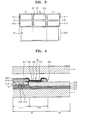
FIG. 9 is a cross-sectional view of a pixel of an organic light emitting display device according to another embodiment of the present invention. - Reference will now be made in detail to the present embodiments of the present invention, examples of which are illustrated in the accompanying drawings, wherein like reference numerals refer to the like elements throughout. The embodiments are described below in order to explain the present invention by referring to the figures.
- Here, it is to be understood that where is stated herein that one film or layer is "formed on" or "disposed on" a second layer or film, the first layer or film may be formed or disposed directly on the second layer or film or there may be intervening layers or films between the first layer or film and the second layer or film. Further, as used herein, the term "formed on" is used with the same meaning as "located on" or "disposed on" and is not meant to be limiting regarding any particular fabrication process.
-
FIG. 1 is a schematic cross-sectional view of an organic light emitting display device according to an embodiment of the present invention. Referring toFIG. 1 , the organic light emitting display device according to an embodiment of the present invention includes asubstrate 1 and adisplay unit 2 placed on thesubstrate 1. External light enters the organic light emitting display device via thedisplay unit 2 and thesubstrate 1. - As will be described later, the
display unit 2 transmits external light. Referring toFIG. 1 , thedisplay unit 2 allows a user positioned below thesubstrate 1 to view external images beyond thedisplay unit 2. Although a bottom-emission type organic light emitting display device in which images on thedisplay unit 2 are displayed toward thesubstrate 1 as illustrated inFIG. 1 , aspects of the present invention are not limited thereto, and may be equally applied to a top-emission type organic light emitting display device in which images on thedisplay unit 2 are displayed in a direction opposite to thesubstrate 1. -
FIG. 1 illustrates two adjacent pixels, namely, a first pixel P1 and a second pixel P2, of the organic light emitting display device according to an aspect of the present invention. - Each of the first and second pixels P1 and P2 includes a
first region 31 and asecond region 32. - An image is displayed on the
display unit 2 in thefirst region 31, and external light passes through thedisplay unit 2 in thesecond region 32. - In other words, since each of the first and second pixels P1 and P2 includes the
first region 31 where images are displayed and thesecond region 32 which transmits external light, a user can see an external image through thesecond region 32 when the user does not see the image displayed through thefirst region 31. - Thus, the
second region 32 does not include devices such as a thin film transistor, a capacitor, and an organic light emitting device, and thus external light transmittance may be maximized and distortion of a transmitted image due to interference of the devices such as a thin film transistor, a capacitor, and an organic light emitting device may be prevented as much as possible. -
FIG. 2 is a schematic plan view of a red pixel Pr, a green pixel Pg, and a blue pixel Pb that are adjacent to one another. - Each of the red, green, and blue pixels Pr, Pg, and Pb includes a
circuit region 311 and anemission region 312 in thefirst region 31. Thecircuit region 311 and theemission region 312 are adjacent to each other. - The
second region 32 that transmits external light is adjacent to thefirst region 31. - As illustrated in
FIG. 2 , independentsecond regions 32 may be included in the red, green, and blue pixels Pr, Pg, and Pb, respectively. Alternatively, as illustrated inFIG. 3 ,second regions 32 may be connected to one another across the red, green, and blue pixels Pr, Pg, and Pb. In the embodiment ofFIG. 3 , an area of thesecond region 32 through which external light passes is increased, and thus the transmittance of theentire display unit 2 may be increased. - Although the
second regions 32 of the red, green, and blue pixels Pr, Pg, and Pb are integrally connected to one another inFIG. 3 , the aspects of the present invention are not limited thereto, and the second regions of only two adjacent pixels from among the red, green, and blue pixels Pr, Pg, and Pb may be connected to each other. -
FIG. 4 illustrates a cross-section of the red, green, or blue pixel Pr, Pg, or Pb illustrated inFIGS. 2 and3 . - As illustrated in
FIG. 4 , a thin film transistor TR is arranged in thecircuit region 311. However, a pixel circuit including the thin film transistor TR may be also included in thecircuit region 311. Alternatively, thecircuit region 311 may further include a plurality of thin film transistors TR and a storage capacitor. In this case, wires such as scan lines, data lines, and Vdd lines connected to the thin film transistors TR and the storage capacitor may be further included in thecircuit region 311. - An organic light emitting diode EL may be disposed in the
emission region 312. The organic light emitting diode EL is electrically connected to the thin film transistor TR of thecircuit region 311. - A
buffer layer 211 is formed on thesubstrate 1, and a pixel circuit including the thin film transistor TR is formed on thebuffer layer 211. - First, a semiconductor
active layer 212 is formed on thebuffer layer 211. - The
buffer layer 211 is formed of a transparent insulation material and prevents impurity elements from penetrating into thesubstrate 1 and planarizes a surface of thesubstrate 1. Thebuffer layer 211 may be formed of any of various materials that can perform the functions described above. For example, thebuffer layer 211 may be formed of an inorganic material such as silicon oxide, silicon nitride, silicon oxynitride, aluminum oxide, aluminum nitride, titanium oxide, or titanium nitride, an organic material such as polyimide, polyester, or acryl, or stacks of these materials. Thebuffer layer 211 is not an essential element and may not be formed at all. - The semiconductor
active layer 212 may be formed of polycrystal silicon, but is not limited thereto and may be formed of a semiconductor oxide. For example, the semiconductoractive layer 212 may be a G-I-Z-O layer [a(In2O3)b(Ga2O3)c(ZnO) layer] (where a, b, and c are natural numbers that respectively satisfy a≥0, b≥0, and c>0). When the semiconductoractive layer 212 is formed of a semiconductor oxide, light transmittance in thecircuit region 311 of thefirst region 31 may be increased, and thus external light transmittance of theentire display unit 2 may be increased. - A
gate insulating layer 213 is formed on thebuffer layer 211 so as to cover the semiconductoractive layer 212, and agate electrode 214 is formed on thegate insulating layer 213. - An interlayer insulating
layer 215 is formed on thegate insulating layer 213 so as to cover thegate electrode 214. Asource electrode 216 and adrain electrode 217 are formed on theinterlayer insulating layer 215 so as to contact the semiconductoractive layer 212 via contact holes. - The structure of the thin film transistor TR is not limited to the above-described structure, and the thin film transistor TR may have various other structures.
- A
passivation layer 218 is formed to cover the thin film transistor TR. Thepassivation layer 218 may be a single-layered or multi-layered insulating layer, an upper surface of which is planarized. Thepassivation layer 218 may be formed of an inorganic material and/or an organic material. - As illustrated in
FIG. 4 , afirst electrode 221 of an organic light emitting diode EL electrically connected to the thin film transistor TR is formed on thepassivation layer 218. Thefirst electrode 221 corresponds to each pixel. - An insulating
layer 219 is formed of an organic and/or inorganic insulating material on thepassivation layer 218 to cover at least an edge portion of thefirst electrode 221. - The insulating
layer 219 exposes only a central portion of thefirst electrode 221. Although the insulatinglayer 219 may be included to cover thefirst region 31, the first insulatinglayer 219 does not necessarily cover the entirefirst region 31, and it is sufficient for the insulatinglayer 219 to cover only a part of thefirst region 31, particularly, an edge of thefirst electrode 221. - An
organic layer 223 and asecond electrode 222 are sequentially stacked on thefirst electrode 221. Thesecond electrode 222 covers theorganic layer 223 and the insulatinglayer 219, andsecond electrodes 222 corresponding to all of the pixels are electrically connected to one another. - The
organic layer 223 may be a low molecular weight organic layer or a polymer organic layer. When theorganic layer 223 is a low molecular weight organic layer, theorganic layer 223 may be formed by stacking a hole injection layer (HIL), a hole transport layer (HTL), an emission layer (EML), an electron transport layer (ETL), and an electron injection layer (EIL) in a single structure or a composite structure, and may be formed of any of various materials such as copper phthalocyanine (CuPc), N,N'-Di(naphthalene-1-yl)-N,N'-diphenyl-benzidine (NPB), or tris-8-hydroxyquinoline aluminum (Alq3). The low-molecular weight organic layer may be formed by vacuum deposition. Herein, the HIL, the HTL, the ETL, and the EIL are common layers and may be commonly applied to red, green, and blue pixels. - The
first electrode 221 may function as an anode, and thesecond electrode 222 may function as a cathode. Alternatively, thefirst electrode 221 may function as a cathode, and thesecond electrode 222 may function as an anode. - According to an embodiment of the present invention, the
first electrode 221 may be a transparent electrode, and thesecond electrode 222 may be a reflection electrode. Thefirst electrode 221 may include ITO, IZO, ZnO, In2O3, or the like each having a high work function. Thesecond electrode 222 may be formed of a metal having a low work function, such as Ag, Mg, Al, Pt, Pd, Au, Ni, Nd, Ir, Cr, Li, or Ca. Accordingly, the organic light emitting diode EL is a bottom emission type in which light is emitted towards thefirst electrode 221. - However, the aspects of the present invention are not limited thereto, and the
second electrode 222 may also be a transparent type electrode. - The
passivation layer 218, thegate insulating layer 213, theinterlayer insulating layer 215, and the insulatinglayer 219 may be transparent insulating layers. - A sealing
substrate 4 may be installed over thesecond electrode 222. The sealingsubstrate 4 is located outside thedisplay unit 2 and bonded with thesubstrate 1 by a sealant (not shown) so as to protect thesecond electrode 222 from external air. A filler (not shown) may be filled between the sealingsubstrate 4 and thesecond electrode 222, and a moisture absorbent may also be interposed therebetween. A sealing structure for thedisplay unit 2 is not limited to the use of the sealingsubstrate 4, and a film-shaped sealing structure may be used. -
Transmission windows 224 are further formed in thesecond electrode 222 and the insulatinglayer 219. Thetransmission windows 224 may be formed only in thesecond electrode 222, or may be formed in at least one selected from the group consisting of thepassivation layer 218, theinterlayer insulating layer 215, thegate insulating layer 213, and thebuffer layer 211. - The
transmission windows 224 are formed at locations corresponding to thesecond regions 32. Thetransmission windows 224 may be formed in any pattern such as the one shown inFIGS. 2 and3 . However, it is understood that the transmission windows can have a different pattern than those illustrated inFIGS. 2 and3 . - However, it is difficult to form the
transmission windows 224 in thesecond electrode 222, because a metal for thesecond electrode 222 should be deposited using a mask having a shield portion corresponding to the pattern of thetransmission windows 224 in order to form thetransmission windows 224 in the pattern and manufacturing the mask having the shield portion corresponding to the pattern is very difficult. - A
mask 5 illustrated inFIG. 5 is used to form thesecond electrode 222 having thetransmission windows 224 arranged in such pattern. - The
mask 5 has anaperture 51 corresponding to afirst region 31 of a specific pixel. A pattern of theapertures 51 shown inFIG. 5 is used to form thetransmission windows 224 having the pattern illustrated inFIG. 3 . Themask 5 has anaperture 51 corresponding to thefirst regions 31 of three adjacent pixels, namely, a red pixel, a green pixel, and a blue pixel. The size of theaperture 51 is generally slightly greater than the overall size of the three pixels so that patterns obtained when a material used to form thesecond electrode 222 is deposited via theapertures 51 overlap each other. Thus, thesecond electrode 222 may act as a common electrode. - When the three pixels constitute a unit pixel, the
apertures 51 are separated from one another by a distance corresponding to the unit pixel in a horizontal direction and a vertical direction. - When a metal used to form the
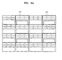
second electrode 222 is deposited on theorganic layer 223 by using themask 5, a pattern illustrated inFIG. 6A is obtained. - When the
mask 5 is shifted by one unit pixel horizontally and then metal is deposited, a pattern as illustrated inFIG. 6B is obtained. When themask 5 is shifted again by one unit pixel downward and then metal is deposited, a pattern as illustrated inFIG. 6C is obtained. Thereafter, when themask 5 is shifted again by one unit pixel horizontally and then metal is deposited, a pattern as illustrated inFIG. 6D is obtained. Thus, as illustrated inFIG. 6D , thesecond electrode 222 having thetransmission windows 224 in the pattern ofFIG. 3 is obtained. - The pattern of the
apertures 51 of themask 5 is not limited to the pattern illustrated inFIG. 5 . In other words, if anaperture 51 is formed at the center of the fouradjacent apertures 51 illustrated inFIG. 5 and theaperture 51 at the center is the same as each of the fouradjacent apertures 51, thesecond electrode 222 having the pattern illustrated inFIG. 6D may be obtained by shifting themask 5 horizontally only once. -
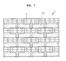
FIGS. 7 and8 illustratemasks 5 having other shapes than themask 5 ofFIG. 5 . - An
aperture 51 corresponding to afirst region 31 corresponding to three pixels is formed around a region corresponding to atransmission window 224. The pattern of theapertures 51 illustrated inFIG. 7 may allow thesecond electrode 222 having the pattern illustrated inFIG. 6D to be obtained by shifting themask 5 horizontally only once. In this case, since an interval betweenapertures 51 is sufficient, themask 5 is not destroyed by a tensile force but may be stable. -
FIG. 8 illustrates a modified example ofFIG. 7 . A center of anaperture 51 protrudes upward and downward, and thus when amask 5 ofFIG. 7 is shifted horizontally by one unit pixel and deposition is performed, deposition occurs redundantly on the upward and downward protrusions of theaperture 51. Thus, thesecond electrode 222 may be stably formed through the entire display unit without any discontinuity. - The above embodiment applies not only to a structure in which a circuit part including the thin film transistor TR is not overlapped by the
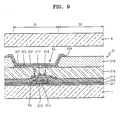
first electrode 221 as illustrated inFIG. 4 but also to a structure in which a circuit part including the thin film transistor TR is overlapped by thefirst electrode 221 as illustrated inFIG. 9 . - In the case of the structure illustrated in
FIG. 9 , when thefirst electrode 221 is formed as a reflection electrode, an effect where a conductive pattern of a circuit part is shielded by thefirst electrode 221 may be obtained. Thus, distortion of a penetrated image due to external light scattered by the conductive pattern of the circuit part may be suppressed. - Although a few embodiments of the present invention have been shown and described, it would be appreciated by those skilled in the art that changes may be made in this embodiment without departing from the principles of the invention, the scope of which is defined in the claims and their equivalents.
Claims (13)
- An organic light emitting display device comprising:a substrate;a plurality of pixels formed on the substrate, each pixel comprising a first region that emits light and a second region that transmits external light;a respective thin film transistor disposed in the first region of each pixel;a respective first electrode disposed in the first region of each pixel and electrically connected to the said thin film transistor disposed in that pixel;a second electrode formed opposite to the plurality of first electrodes and comprising a plurality of transmission windows, wherein each of the transmission windows corresponds in position to a respective one of the second regions; andan organic layer formed between the first electrodes and the second electrode.
- An organic light emitting display device according to claim 1, wherein the transmission windows for at least two adjacent pixels are separated from one another.
- An organic light emitting display device according to claim 1 or 2,
wherein the transmission windows in at least two adjacent pixels are connected to each other. - An organic light emitting display device according to any preceding claim, wherein the second electrode comprises a light-reflection material.
- An organic light emitting display device according to any preceding claim, wherein the plurality of first electrodes comprise a light-transmission material.
- An organic light emitting display device according to any preceding claim, wherein the plurality of first electrodes overlap the plurality of thin film transistors.
- An organic light emitting display device according to any preceding claim, wherein the first region of each pixel comprises an emission region and a circuit region, each thin film transistor is disposed in a respective said circuit region, and each first electrode is disposed in a respective said emission region.
- An organic light emitting display device according to claim 7, wherein the emission region and the circuit region of each pixel are adjacent to each other.
- An organic light emitting display device according to any preceding claim, wherein the first region of each pixel is adapted to display an image, and the second region of each pixel is adapted to transmit light.
- An organic light emitting display device according to any preceding claim, wherein the second region of each pixel does not include a thin film transistor, a capacitor and an organic light emitting device.
- A method of manufacturing an organic light emitting display device, the method comprising:defining a plurality of pixels on a substrate, each of the pixels comprising a first region that emits light and a second region that transmits external light;forming a respective thin film transistor in the first region of each pixel;forming a respective first electrode in the first region of each pixel, the said first electrode being electrically connected to the thin film transistor located in that pixel;forming an organic layer on the plurality of first electrodes; andforming a second electrode on the organic layer by using a mask having a pattern of apertures corresponding to the first regions, wherein the second electrode comprises a plurality of transmission windows that correspond in position to the location of the second regions.
- A method according to claim 11, wherein the apertures are separated from each other at regular intervals.
- A method according to claim 12, wherein the apertures are separated from each other at intervals smaller than or equal to a distance corresponding to at least one pixel.
Applications Claiming Priority (1)
| Application Number | Priority Date | Filing Date | Title |
|---|---|---|---|
| KR1020100021384A KR20110101980A (en) | 2010-03-10 | 2010-03-10 | OLED display and manufacturing method thereof |
Publications (2)
| Publication Number | Publication Date |
|---|---|
| EP2365557A2 true EP2365557A2 (en) | 2011-09-14 |
| EP2365557A3 EP2365557A3 (en) | 2014-05-14 |
Family
ID=44260774
Family Applications (1)
| Application Number | Title | Priority Date | Filing Date |
|---|---|---|---|
| EP11250277.8A Withdrawn EP2365557A3 (en) | 2010-03-10 | 2011-03-10 | Organic light emitting display device and method of manufacturing the same |
Country Status (6)
| Country | Link |
|---|---|
| US (4) | US9490311B2 (en) |
| EP (1) | EP2365557A3 (en) |
| JP (1) | JP5687865B2 (en) |
| KR (1) | KR20110101980A (en) |
| CN (1) | CN102194854B (en) |
| TW (1) | TWI545742B (en) |
Cited By (2)
| Publication number | Priority date | Publication date | Assignee | Title |
|---|---|---|---|---|
| EP2866262A1 (en) * | 2013-10-18 | 2015-04-29 | Samsung Display Co., Ltd. | Organic light emitting display device |
| EP2672541A3 (en) * | 2012-06-07 | 2016-09-14 | Samsung Display Co., Ltd. | Display apparatus capable of controlling light transmittance |
Families Citing this family (37)
| Publication number | Priority date | Publication date | Assignee | Title |
|---|---|---|---|---|
| JP6235475B2 (en) | 2011-10-28 | 2017-11-22 | コーニンクレッカ フィリップス エヌ ヴェKoninklijke Philips N.V. | Transparent OLED device with structured cathode and method for manufacturing such OLED device |
| KR101829890B1 (en) | 2011-12-23 | 2018-02-20 | 삼성디스플레이 주식회사 | Organic light emitting display apparatus and method of manufacturing the same |
| KR101275810B1 (en) | 2012-01-20 | 2013-06-18 | 삼성디스플레이 주식회사 | Organic light emitting display device |
| TWI478412B (en) * | 2012-09-06 | 2015-03-21 | Ultimate Image Corp | Organic light emitting device and power supply thereof |
| KR102237117B1 (en) | 2014-09-01 | 2021-04-08 | 삼성디스플레이 주식회사 | Organic light emitting display device |
| JP6522311B2 (en) * | 2014-10-17 | 2019-05-29 | パイオニア株式会社 | Light emitting device |
| CN111263483B (en) | 2015-02-25 | 2023-04-07 | 日本先锋公司 | Light emitting device, method for manufacturing light emitting device, and light emitting system |
| JP6457065B2 (en) | 2015-03-09 | 2019-01-23 | パイオニア株式会社 | Light emitting device |
| KR102453420B1 (en) * | 2015-04-30 | 2022-10-13 | 삼성디스플레이 주식회사 | Transparent organic light emitting display device and method of manufacturing organic light emitting display device |
| KR102515963B1 (en) * | 2016-03-04 | 2023-03-30 | 삼성디스플레이 주식회사 | Organic light emitting display panel |
| KR102694860B1 (en) | 2016-09-23 | 2024-08-13 | 삼성디스플레이 주식회사 | Display device and manufacturing method thereof |
| KR102722245B1 (en) * | 2016-10-14 | 2024-10-25 | 삼성디스플레이 주식회사 | Display device and manufacturing method thereof |
| CN108520891B (en) * | 2018-04-20 | 2020-08-04 | 京东方科技集团股份有限公司 | Inkjet printing method for array substrate, array substrate, and display device |
| KR102668689B1 (en) * | 2018-05-10 | 2024-05-24 | 삼성디스플레이 주식회사 | Display apparatus and Manufacturing method thereof |
| KR102573917B1 (en) * | 2018-06-14 | 2023-09-04 | 엘지디스플레이 주식회사 | Display Device and Manufacturing the Same |
| JP6837045B2 (en) * | 2018-12-19 | 2021-03-03 | パイオニア株式会社 | Light emitting device |
| KR102778472B1 (en) | 2019-02-08 | 2025-03-12 | 삼성디스플레이 주식회사 | Display apparatus and the manufacturing method thereof |
| KR102783287B1 (en) * | 2019-03-04 | 2025-03-20 | 삼성디스플레이 주식회사 | Organic light emitting display device |
| US11341878B2 (en) * | 2019-03-21 | 2022-05-24 | Samsung Display Co., Ltd. | Display panel and method of testing display panel |
| CN109962096B (en) * | 2019-04-15 | 2021-02-23 | 京东方科技集团股份有限公司 | Display back plate, manufacturing method thereof and display device |
| JP2019117958A (en) * | 2019-04-24 | 2019-07-18 | パイオニア株式会社 | Light-emitting device |
| KR102787861B1 (en) * | 2019-04-29 | 2025-04-01 | 삼성디스플레이 주식회사 | Display panel and display apparatus including the same |
| KR20200136549A (en) | 2019-05-27 | 2020-12-08 | 삼성디스플레이 주식회사 | Display apparatus and Method of manufacturing of the same |
| KR20200136551A (en) * | 2019-05-27 | 2020-12-08 | 삼성디스플레이 주식회사 | Display device |
| KR102914150B1 (en) * | 2019-06-26 | 2026-01-16 | 삼성디스플레이 주식회사 | Display device |
| KR102830962B1 (en) * | 2019-06-28 | 2025-07-08 | 삼성디스플레이 주식회사 | Display apparatus and Method of manufacturing of the same |
| KR20210009479A (en) | 2019-07-16 | 2021-01-27 | 삼성디스플레이 주식회사 | Display apparatus, apparatus and method for manufacturing the same |
| KR102932280B1 (en) * | 2019-07-25 | 2026-02-27 | 삼성디스플레이 주식회사 | Display apparatus, apparatus and method for manufacturing the same |
| WO2021018304A1 (en) | 2019-07-31 | 2021-02-04 | 京东方科技集团股份有限公司 | Display substrate and display device |
| CN112820763B (en) * | 2019-07-31 | 2024-06-28 | 京东方科技集团股份有限公司 | Electroluminescent display panel and display device |
| KR20210032599A (en) | 2019-09-16 | 2021-03-25 | 삼성디스플레이 주식회사 | Display apparatus |
| CN110649179B (en) * | 2019-09-29 | 2023-05-23 | 京东方科技集团股份有限公司 | A display substrate and its preparation method, a display device, and a mask |
| KR102884491B1 (en) * | 2019-11-29 | 2025-11-11 | 엘지디스플레이 주식회사 | Transparent display device and manufacturing method of the same |
| KR20210085902A (en) * | 2019-12-31 | 2021-07-08 | 엘지디스플레이 주식회사 | Display device |
| US11903252B2 (en) * | 2020-05-15 | 2024-02-13 | Hefei Boe Joint Technology Co., Ltd. | Display panel and electronic device |
| EP3933931A1 (en) | 2020-07-02 | 2022-01-05 | LG Display Co., Ltd. | Display panel and method of fabricating the same |
| KR102909632B1 (en) * | 2020-09-07 | 2026-01-07 | 엘지디스플레이 주식회사 | Display apparatus and method for manufacturing the same |
Family Cites Families (18)
| Publication number | Priority date | Publication date | Assignee | Title |
|---|---|---|---|---|
| JPS6155981A (en) * | 1984-08-27 | 1986-03-20 | Kokusai Denshin Denwa Co Ltd <Kdd> | Semiconductor light-emitting element |
| JP2002231449A (en) | 2001-02-05 | 2002-08-16 | Tohoku Pioneer Corp | Organic el display and method of manufacture |
| JP4887585B2 (en) | 2001-08-24 | 2012-02-29 | パナソニック株式会社 | Display panel and information display device using the same |
| KR100757574B1 (en) | 2001-09-14 | 2007-09-10 | 엘지전자 주식회사 | Organic Electroluminescent Device Mask |
| KR100490322B1 (en) * | 2003-04-07 | 2005-05-17 | 삼성전자주식회사 | Organic electro-luminescent display |
| JP4759511B2 (en) | 2004-04-19 | 2011-08-31 | 株式会社日立製作所 | Imaging function integrated display device |
| JP4752240B2 (en) * | 2004-10-27 | 2011-08-17 | セイコーエプソン株式会社 | Display device and electronic device |
| KR100600883B1 (en) * | 2004-11-11 | 2006-07-18 | 삼성에스디아이 주식회사 | Organic electroluminescent device and manufacturing method thereof |
| JP2007114257A (en) * | 2005-09-20 | 2007-05-10 | Epson Imaging Devices Corp | Liquid crystal display device and electronic apparatus |
| US20070069995A1 (en) * | 2005-09-28 | 2007-03-29 | Shin Hyun S | Flat panel display and a method of driving the same |
| JP2007103028A (en) * | 2005-09-30 | 2007-04-19 | Sanyo Electric Co Ltd | Organic electroluminescent display device |
| US7821613B2 (en) | 2005-12-28 | 2010-10-26 | Semiconductor Energy Laboratory Co., Ltd. | Display device and manufacturing method thereof |
| TW200732733A (en) * | 2006-02-17 | 2007-09-01 | Ind Tech Res Inst | Hybrid display |
| JP5106823B2 (en) | 2006-10-31 | 2012-12-26 | 京セラディスプレイ株式会社 | Light emitting device |
| KR100810641B1 (en) | 2007-03-07 | 2008-03-07 | 삼성에스디아이 주식회사 | Organic electroluminescent display |
| KR100846711B1 (en) * | 2007-03-13 | 2008-07-16 | 삼성에스디아이 주식회사 | OLED display and manufacturing method thereof |
| US20080278063A1 (en) * | 2007-05-07 | 2008-11-13 | Cok Ronald S | Electroluminescent device having improved power distribution |
| KR101378439B1 (en) * | 2008-08-20 | 2014-03-28 | 삼성디스플레이 주식회사 | Organic light emitting diode display and method for manufacturing the same |
-
2010
- 2010-03-10 KR KR1020100021384A patent/KR20110101980A/en not_active Ceased
- 2010-08-18 JP JP2010183437A patent/JP5687865B2/en active Active
-
2011
- 2011-03-02 US US13/038,836 patent/US9490311B2/en active Active
- 2011-03-08 TW TW100107650A patent/TWI545742B/en active
- 2011-03-09 CN CN201110059255.1A patent/CN102194854B/en active Active
- 2011-03-10 EP EP11250277.8A patent/EP2365557A3/en not_active Withdrawn
-
2016
- 2016-11-04 US US15/343,315 patent/US9847486B2/en not_active Ceased
-
2019
- 2019-12-18 US US16/719,751 patent/USRE49965E1/en active Active
-
2024
- 2024-04-29 US US18/649,415 patent/USRE50487E1/en active Active
Non-Patent Citations (1)
| Title |
|---|
| None |
Cited By (5)
| Publication number | Priority date | Publication date | Assignee | Title |
|---|---|---|---|---|
| EP2672541A3 (en) * | 2012-06-07 | 2016-09-14 | Samsung Display Co., Ltd. | Display apparatus capable of controlling light transmittance |
| EP2866262A1 (en) * | 2013-10-18 | 2015-04-29 | Samsung Display Co., Ltd. | Organic light emitting display device |
| EP2866261A1 (en) * | 2013-10-18 | 2015-04-29 | Samsung Display Co., Ltd. | Organic light emitting display device |
| US9679949B2 (en) | 2013-10-18 | 2017-06-13 | Samsung Display Co., Ltd. | Organic light emitting display device |
| US10418428B2 (en) | 2013-10-18 | 2019-09-17 | Samsung Display Co., Ltd. | Organic light emitting display device |
Also Published As
| Publication number | Publication date |
|---|---|
| KR20110101980A (en) | 2011-09-16 |
| JP2011187431A (en) | 2011-09-22 |
| US20110220899A1 (en) | 2011-09-15 |
| CN102194854B (en) | 2016-03-23 |
| EP2365557A3 (en) | 2014-05-14 |
| CN102194854A (en) | 2011-09-21 |
| US9490311B2 (en) | 2016-11-08 |
| USRE50487E1 (en) | 2025-07-08 |
| TW201138094A (en) | 2011-11-01 |
| USRE49965E1 (en) | 2024-05-07 |
| US20170077404A1 (en) | 2017-03-16 |
| TWI545742B (en) | 2016-08-11 |
| JP5687865B2 (en) | 2015-03-25 |
| US9847486B2 (en) | 2017-12-19 |
Similar Documents
| Publication | Publication Date | Title |
|---|---|---|
| USRE50487E1 (en) | Display device and manufacturing method thereof | |
| US8530910B2 (en) | Organic light emitting display device including transmitting regions between pixel regions | |
| US10840481B2 (en) | Organic light-emitting display apparatus and method of manufacturing the same | |
| KR101223727B1 (en) | Organic light emitting display device and manufacturing method thereof | |
| US8659218B2 (en) | Organic light emitting display device | |
| US8629463B2 (en) | Organic light-emitting display device | |
| US9905802B2 (en) | Organic light emitting display apparatus and method of manufacturing the same | |
| US8822998B2 (en) | Organic light emitting display device | |
| US9099674B2 (en) | Organic light-emitting display device | |
| US8598582B2 (en) | Organic light emitting display device | |
| US8274090B2 (en) | Organic light-emitting display device | |
| KR101146984B1 (en) | Organic light emitting display device | |
| US8872206B2 (en) | Organic light emitting display device and method of manufacturing the same | |
| US8797239B2 (en) | Organic light-emitting display device | |
| US8421342B2 (en) | Organic light-emitting display device | |
| US8461592B2 (en) | Organic light emitting display device | |
| US9634072B2 (en) | Organic light-emitting display device and method of manufacturing the same | |
| KR20160027609A (en) | Organic light emitting display apparatus |
Legal Events
| Date | Code | Title | Description |
|---|---|---|---|
| PUAI | Public reference made under article 153(3) epc to a published international application that has entered the european phase |
Free format text: ORIGINAL CODE: 0009012 |
|
| 17P | Request for examination filed |
Effective date: 20110331 |
|
| AK | Designated contracting states |
Kind code of ref document: A2 Designated state(s): AL AT BE BG CH CY CZ DE DK EE ES FI FR GB GR HR HU IE IS IT LI LT LU LV MC MK MT NL NO PL PT RO RS SE SI SK SM TR |
|
| AX | Request for extension of the european patent |
Extension state: BA ME |
|
| RAP1 | Party data changed (applicant data changed or rights of an application transferred) |
Owner name: SAMSUNG DISPLAY CO., LTD. |
|
| PUAL | Search report despatched |
Free format text: ORIGINAL CODE: 0009013 |
|
| RBV | Designated contracting states (corrected) |
Designated state(s): AL AT BE BG CH CY CZ DE DK EE ES FI FR GB GR HR HU IE IS IT LI LT LU LV MC MK MT NL NO PL PT RO RS SE SI SK SM TR |
|
| AK | Designated contracting states |
Kind code of ref document: A3 Designated state(s): AL AT BE BG CH CY CZ DE DK EE ES FI FR GB GR HR HU IE IS IT LI LT LU LV MC MK MT NL NO PL PT RO RS SE SI SK SM TR |
|
| AX | Request for extension of the european patent |
Extension state: BA ME |
|
| RIC1 | Information provided on ipc code assigned before grant |
Ipc: H01L 51/52 20060101AFI20140409BHEP Ipc: H01L 27/32 20060101ALI20140409BHEP |
|
| RAP1 | Party data changed (applicant data changed or rights of an application transferred) |
Owner name: SAMSUNG DISPLAY CO., LTD. |
|
| STAA | Information on the status of an ep patent application or granted ep patent |
Free format text: STATUS: THE APPLICATION IS DEEMED TO BE WITHDRAWN |
|
| 18D | Application deemed to be withdrawn |
Effective date: 20171003 |