EP2365498A1 - Switch and method for manufacturing the same, and relay - Google Patents
Switch and method for manufacturing the same, and relay Download PDFInfo
- Publication number
- EP2365498A1 EP2365498A1 EP11151193A EP11151193A EP2365498A1 EP 2365498 A1 EP2365498 A1 EP 2365498A1 EP 11151193 A EP11151193 A EP 11151193A EP 11151193 A EP11151193 A EP 11151193A EP 2365498 A1 EP2365498 A1 EP 2365498A1
- Authority
- EP
- European Patent Office
- Prior art keywords
- contact
- substrate
- conductive layer
- contacts
- switch
- Prior art date
- Legal status (The legal status is an assumption and is not a legal conclusion. Google has not performed a legal analysis and makes no representation as to the accuracy of the status listed.)
- Withdrawn
Links
- 238000000034 method Methods 0.000 title claims description 25
- 238000004519 manufacturing process Methods 0.000 title claims description 21
- 239000000758 substrate Substances 0.000 claims abstract description 86
- 238000009713 electroplating Methods 0.000 claims abstract description 13
- 238000007740 vapor deposition Methods 0.000 claims description 8
- 238000004544 sputter deposition Methods 0.000 claims description 7
- 238000000151 deposition Methods 0.000 claims description 4
- 239000000463 material Substances 0.000 claims description 4
- VYPSYNLAJGMNEJ-UHFFFAOYSA-N Silicium dioxide Chemical compound O=[Si]=O VYPSYNLAJGMNEJ-UHFFFAOYSA-N 0.000 description 12
- 238000007747 plating Methods 0.000 description 8
- 238000005530 etching Methods 0.000 description 7
- 238000005498 polishing Methods 0.000 description 7
- 229910052681 coesite Inorganic materials 0.000 description 6
- 229910052906 cristobalite Inorganic materials 0.000 description 6
- 239000000377 silicon dioxide Substances 0.000 description 6
- 229910052682 stishovite Inorganic materials 0.000 description 6
- 229910052905 tridymite Inorganic materials 0.000 description 6
- 239000002184 metal Substances 0.000 description 4
- 229910052751 metal Inorganic materials 0.000 description 4
- 229910052802 copper Inorganic materials 0.000 description 3
- 150000004767 nitrides Chemical class 0.000 description 3
- PNEYBMLMFCGWSK-UHFFFAOYSA-N aluminium oxide Inorganic materials [O-2].[O-2].[O-2].[Al+3].[Al+3] PNEYBMLMFCGWSK-UHFFFAOYSA-N 0.000 description 2
- 230000000694 effects Effects 0.000 description 2
- 230000002708 enhancing effect Effects 0.000 description 2
- 239000011521 glass Substances 0.000 description 2
- 239000007769 metal material Substances 0.000 description 2
- 239000002923 metal particle Substances 0.000 description 2
- 238000000059 patterning Methods 0.000 description 2
- 238000000206 photolithography Methods 0.000 description 2
- 229920002120 photoresistant polymer Polymers 0.000 description 2
- 239000002244 precipitate Substances 0.000 description 2
- 229910001020 Au alloy Inorganic materials 0.000 description 1
- 229910001260 Pt alloy Inorganic materials 0.000 description 1
- 238000005452 bending Methods 0.000 description 1
- 238000004140 cleaning Methods 0.000 description 1
- 239000004020 conductor Substances 0.000 description 1
- 229910052593 corundum Inorganic materials 0.000 description 1
- 230000005684 electric field Effects 0.000 description 1
- 229910052737 gold Inorganic materials 0.000 description 1
- 238000009499 grossing Methods 0.000 description 1
- 230000002401 inhibitory effect Effects 0.000 description 1
- 230000001788 irregular Effects 0.000 description 1
- 229910052763 palladium Inorganic materials 0.000 description 1
- 229910052697 platinum Inorganic materials 0.000 description 1
- 229910052702 rhenium Inorganic materials 0.000 description 1
- 229910052703 rhodium Inorganic materials 0.000 description 1
- 229910052707 ruthenium Inorganic materials 0.000 description 1
- 239000000126 substance Substances 0.000 description 1
- XLYOFNOQVPJJNP-UHFFFAOYSA-N water Substances O XLYOFNOQVPJJNP-UHFFFAOYSA-N 0.000 description 1
- 229910001845 yogo sapphire Inorganic materials 0.000 description 1
Images





Classifications
-
- H—ELECTRICITY
- H01—ELECTRIC ELEMENTS
- H01H—ELECTRIC SWITCHES; RELAYS; SELECTORS; EMERGENCY PROTECTIVE DEVICES
- H01H1/00—Contacts
- H01H1/0036—Switches making use of microelectromechanical systems [MEMS]
-
- H—ELECTRICITY
- H01—ELECTRIC ELEMENTS
- H01H—ELECTRIC SWITCHES; RELAYS; SELECTORS; EMERGENCY PROTECTIVE DEVICES
- H01H1/00—Contacts
- H01H1/02—Contacts characterised by the material thereof
- H01H1/021—Composite material
- H01H1/023—Composite material having a noble metal as the basic material
-
- H—ELECTRICITY
- H01—ELECTRIC ELEMENTS
- H01H—ELECTRIC SWITCHES; RELAYS; SELECTORS; EMERGENCY PROTECTIVE DEVICES
- H01H1/00—Contacts
- H01H1/06—Contacts characterised by the shape or structure of the contact-making surface, e.g. grooved
-
- H—ELECTRICITY
- H01—ELECTRIC ELEMENTS
- H01H—ELECTRIC SWITCHES; RELAYS; SELECTORS; EMERGENCY PROTECTIVE DEVICES
- H01H59/00—Electrostatic relays; Electro-adhesion relays
- H01H59/0009—Electrostatic relays; Electro-adhesion relays making use of micromechanics
-
- H—ELECTRICITY
- H01—ELECTRIC ELEMENTS
- H01H—ELECTRIC SWITCHES; RELAYS; SELECTORS; EMERGENCY PROTECTIVE DEVICES
- H01H1/00—Contacts
- H01H1/0036—Switches making use of microelectromechanical systems [MEMS]
- H01H2001/0052—Special contact materials used for MEMS
-
- H—ELECTRICITY
- H01—ELECTRIC ELEMENTS
- H01H—ELECTRIC SWITCHES; RELAYS; SELECTORS; EMERGENCY PROTECTIVE DEVICES
- H01H1/00—Contacts
- H01H1/0036—Switches making use of microelectromechanical systems [MEMS]
- H01H2001/0078—Switches making use of microelectromechanical systems [MEMS] with parallel movement of the movable contact relative to the substrate
Definitions
- the present invention relates to a switch and a method for manufacturing the same, and a relay. Specifically, the present invention relates to a switch using a metallic contact and a method for manufacturing the same, and also to a relay that uses the structure of the switch.
- a MEMS switch for bringing into contact with and separating from the metallic contact is, for example, disclosed in Japanese Unexamined Patent Publication No. 2006-526267 .
- a switch 11 in a switch 11, an insulating layer 13a is formed on an upper surface of a substrate 12a, a conductive layer 14a made of Al, Cu, or the like is formed thereon, and a plated layer 15a of Au or the like is grown from the upper surface to the end face of the conductive layer 14a to form a movable contact portion 17.
- an insulating layer 13b is formed on an upper surface of a substrate 12b, a conductive layer 14b made of Al, Cu, or the like is formed thereon, and a plated layer 15b of Au or the like is grown from the upper surface to the end face of the conductive layer 14b to form a fixed contact portion 18.
- a switching operation is carried out between the movable contact portion 17 and the fixed contact portion 18 by moving the movable contact portion 17 in the direction of the arrow, and bringing into contact with or separating from a movable contact 16a that is a projecting region of the plated layer 15a and a fixed contact 16b that is a projecting region of the plated layer 15b.
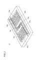
- An electrostatic relay is disclosed in Japanese Unexamined Patent Publication No. 9-251834 and the like.
- a lever 24a is elastically bent by applying voltage to a movable comb teeth like electrode 22a and a fixed comb teeth like electrode 23a
- a lever 24b is elastically bent by applying voltage to a movable comb teeth like electrode 22b and a fixed comb teeth like electrode 23b, so that a movable contact 25a formed at the distal end of the lever 24a and a movable contact 25b formed at the distal end of the lever 24b are in contact with each other thereby closing between the movable contacts 25a, 25b.
- the movable contacts 25a, 25b are opened and separated by releasing the application voltage between each comb teeth like electrode 22a and 23a and the movable comb teeth like electrode 22b and 23b.
- the movable contacts 25a, 25b are formed by forming a metal film on the distal ends of the levers 24a, 24b through vapor deposition, sputtering, and the like.
- the surfaces (surfaces of contacts) perpendicular to the growing direction of such contacts are considerably rough when viewed microscopically, and have irregular microscopic bumps.
- the contacting area of the contacts is thus small when seen microscopically, and the contact resistance in the case where the contacts are closed is large.
- the contact resistance between the contacts tends to become unnecessarily large since the parallelism of the surfaces of the opposing contacts is difficult to obtain.
- the growing speed of the contact is large since the electric field intensity is high at the end face of the conductive layer in the switch 11 as well as the end face of the lever in the electrostatic relay 21, and hence, the gap distance between the contacts is difficult to control. Thus, the distance between the contacts becomes difficult to narrow.
- a method of smoothing the surface of the contact by polishing and the like is known to resolve such drawbacks, but this increases the polishing step of the contact and becomes a factor in increase in cost of the switch and the relay.
- the present invention has been devised to solve the problems described above, and an object thereof is to provide a switch capable of smoothly forming a contacting surface of a contact without performing polishing, and the like and a method for manufacturing the same, as well as, a relay that uses the structure of the switch.
- a switch according to the present invention relates to a switch including a plurality of contacts that bring into contact with or separate from each other, wherein a surface parallel to a growing direction when forming a conductive layer for forming the contacts is a contacting surface of the contacts.
- the contacting surface of the contact can be formed smooth without performing polishing and the like of the contact since the contacting surfaces of the contacts are surfaces parallel to the growing direction of the conductive layer.
- the contact resistance in the case where the contacts come into contact with each other thus becomes small. If the contacting surfaces of the contacts are smooth, the contacts come into contact with each other evenly, and hence the contact contacting portion is less likely to break. As a result, the open/dose lifespan of the switch becomes longer, and the distance between the contacts can be narrowed.
- the contacting surface of the contact is a surface contacting a mold portion for defining a forming region of the conductive layer when growing the conductive layer.
- the contacting surface of the contact can be formed smooth since the contacting surface of the contact can be formed using the surface of the mold portion.
- a method for manufacturing a switch relates to a method for manufacturing a switch including a plurality of contacts that bring into contact with or separate from each other, the method comprising the steps of forming a mold portion of a predetermined pattern on an upper side of a substrate, growing a conductive layer in a thickness direction of the substrate in a plurality of regions excluding a region formed with the mold portion at the upper side of the substrate, removing the mold portion and having a surface contacting a side surface of the mold portion of the conductive layer as contacting surfaces of the contacts, and dividing the substrate into plurals in accordance with the plurality of regions formed with the conductive layer.
- the contacting surface of the contact can be formed smooth without performing the polishing and the like of the contact since the contacting surface of the contact can be molded by the side surface of the mold portion when forming the conductive layer.
- the contact resistance in the case where the contacts come into contact with each other thus becomes small.
- the contacting surfaces of the contacts become smooth, the contacting positions of the contacts are dispersed, and the contact contacting portion becomes less likely to break. As a result, the open/dose lifespan of the switch becomes longer, and the distance between the contacts can be narrowed.
- both side surfaces of the mold portion for forming the opposing contacts are formed parallel to each other.
- the contacting surfaces of the contacts can be made parallel to each other.
- the conductive layer may be grown on the upper side of the substrate through an electrolytic plating or a non-electrolytic plating, or may be grown on the upper side of the substrate through a deposition method such as vapor deposition and sputtering.
- a deposition method such as vapor deposition and sputtering.
- the material of the conductive layer deposited on the mold portion can be removed with the mold portion in the step of removing the mold portion.
- a relay according to the present invention includes the switch according to the present invention, and an actuator for moving one part of the contact in a direction perpendicular to the contacting surfaces of the contacts to bring into contact with or separate from the contactseach other.
- the contact resistance in the case where the contacts come into contacts with each other can be reduced since the contacting surfaces of the contacts can be formed smooth. If the contacting surfaces of the contacts are smooth, the contacts come into contact with each other evenly, and hence the contact contacting portion is less likely to break. As a result, the lifespan of the relay becomes longer.
- the means for solving the problems in the present invention have characteristics in which the configuring elements described above are appropriately combined, where the present invention includes a great number of variations obtained by combining the configuring elements.
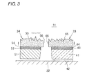
- Fig. 3 is a cross-sectional view showing a structure of a switch according to a first embodiment of the present invention.
- the switch 31 includes a fixed contact portion 33 and a movable contact portion 34.
- the fixed contact portion 33 is fixed to an upper surface of a base substrate 32 through an insulating film 42, and the movable contact portion 34 moves in a direction (direction indicated with outlined arrow) parallel to the upper surface of the base substrate 32 by a drive mechanism or an actuator.
- the switch of the present invention can be used in a MEMS switch having the structure dislosed in Japanese Unexamined Patent Publication No. 2006-526267 .
- the fixed contact portion 33 is obtained by forming an insulating 43 and a base layer 44 on the upper surface of a fixed contact substrate 41, and forming a conductive layer 45 thereon.
- the movable contact portion 34 is obtained by forming an insulating 53 and a base layer 54 on the upper surface of a movable contact substrate 51, and forming a conductive layer 55 thereon.
- the conductive layers 45, 55 are formed by growing a conductive material in the thickness direction (direction of arrow in Fig. 3 ) through electrolytic plating and non-electrolytic plating, vapor deposition, sputtering and the like, where the respective opposing side surfaces become a fixed contact 46 (electrical contacting surface) and a movable contact 56 (electrical contacting surfaces).
- the material of the conductive layers 45, 55 may be Pt, Au, Pd, lr, Ru, Rh, Re, Ta, Pt alloy, Au alloy and the like.
- the fixed contact 46 and the movable contact 56 are smoothly formed parallel to each other. Therefore, when the movable contact portion 34 is parallel moved so that the fixed contact 46 and the movable contact 56 bring into contact with each other to close the contacts 46, 56, the contacts 46, 56 are in contact with over substantially the entire surface.
- the opposing portions of the conductive layer 45 and the conductive layer 55 respectively project out from the end face of the fixed contact substrate 41 and the movable contact substrate 51, and the opposing surfaces of the fixed contact substrate 41 and the movable contact substrate 51 are both inclined to retreat toward the lower surface side. Therefore, when moving the movable contact portion 34 to bring contact the movable contact 56 into contact with the fixed contact 46, the fixed contact substrate 41 and the movable contact substrate 51 are not in contact with each other thereby inhibiting the contact of the movable contact 56 and the fixed contact 46.
- the switch 31 is formed using a MEMS (Micro Electrical-Mechanical Systems) technique.
- the manufacturing method shown in Fig. 4A to Fig. 4D forms the conducive layers 45, 55 by electrolytic plating.
- Fig. 4A shows that in which an insulating layer A3 such as SiO 2 and a plated base layer A4 are formed on a substrate A1 made of Si, and a mould portion A2 is formed on the plated base layer A4.
- the plated base layer A4 becomes a plated electrode and has two-layer structure including the lower layer Cr / upper layer Au, and has the function of enhancing the adhesiveness (stripping strength) of the insulating layer A3 and the conductive layer A5.
- the mold portion A2 uses a material that has resistance to plating solution and that is selectively etching removed without corroding the conductive layer A5 in the subsequent mold portion removing step.
- the mold portion A2 may be formed by exposing a photoresist applied on the upper surface of the plated base layer A4 through an exposure mask, and patterning by etching.
- the mold portion A2 may be obtained by forming an oxide film (SiO 2 ), a nitride film (SiN), an alumina film (Al 2 O 3 ), and a metal film of a type different from the conductive layers 45 and 55 on the upper surface of the plated base layer A4, and then patterning such films using the photolithography technique.
- the mold portion A2 is thus formed in the region other than the region to form the conductive layers 45, 55, and both side surfaces of the mold portion A2 patterned between the regions to form the conductive layers 45, 55 become parallel to each other and also smooth.
- the entire lower surface of the substrate A1 is fixed to the upper surface of the base substrate 32 including an Si substrate, a glass substrate, or the like through the insulating film 42 such as the SiO 2 .
- the substrate A1 is then immersed in a plating bath and electrolytic plating is carried out with the plated base layer A4 as the plating electrode, so that the plating metal particles such as Pt gradually precipitate on the surface of the plated base layer A4 and the conductive layer A5 grows in the thickness direction of the substrate A1, as shown in Fig. 4B .
- the plating metal particles do not precipitate at the region covered by the mold portion A2.
- the non-electrolytic plating (chemical plating) may be performed instead of the electrolytic plating.
- the mold portion A2 is removed by etching, so that a cavity A6 forms at the area where the mold portion A2 existed between the regions to form the conductive layers 45, 55, as shown in Fig. 4C .
- One conductive layer A5 separated by the cavity A6 becomes the conductive layer 55, and the side surface facing the cavity A6 becomes the movable contact 56.
- the other conductive layer A5 separated by the cavity A6 becomes the conductive layer 45, and the side surface facing the cavity A6 becomes the fixed contact 46.
- etchant is infiltrated from the cavity A6 to sequentially divide the plated base layer A4 and the insulating layer A3 into two. Furthermore, the substrate A1 is etched from the lower surface side or etched from the cavity A6 side to divide into two, where one becomes the base layer 54, the insulating layer, 53 and the movable contact substrate 51 and the other becomes the base layer 44, the insulating layer 43, and the fixed contact substrate 41.
- One of the blocks thus becomes the fixed contact portion 33 where the fixed contact substrate 41, the insulating layer 43, the base layer 44, and the conductive layer 45 are stacked.
- the fixed contact portion 33 is fixed to the upper surface of the base substrate 32 through the insulating film 42.
- the other block becomes the movable contact portion 34 where the movable contact substrate 51, the insulating layer 53, the base layer 54, and the conductive layer 55 are stacked.
- the movable contact portion 34 is separated from the base substrate 32 by lastly removing the insulating film at the lower surface through etching, whereby the switch 31 (MEMS switch) is formed.
- the switch 31 may be formed through steps shown in Figs. 5A to 5D .
- This manufacturing method forms the conducive layers 45, 55 by vapor deposition, sputtering, and the like.
- Fig. 5A is a step corresponding to Fig. 4A , but a adhesion layer A7 (e.g., two-layer structure of lower layer Cr / upper layer Au) for enhancing the adhesion strength (stripping strength) of the insulating layer A3 and the conductive layer A5 is formed in place of the plated base layer A4 on the insulating layer A3.
- the metal material such as Pt is deposited on the adhesion layer A7 through vapor deposition, sputtering, and the like.
- the conductive layer A5 is also deposited on the mold portion A2 as shown in Fig. 5B according to the deposition method through vapor deposition, sputtering, and the like, but the conductive layer A5 on the mold portion A2 is simultaneously removed when removing the mold portion A2 through etching if the mold portion A2 has sufficient height (lift off method).
- the cavity A6 forms after the mold portion A2 is removed as shown in Fig. 5C , and the conductive layer A5 is separated to the conductive layer 55 and the conductive layer 45, which is the same as the step of Fig. 4C . Furthermore, as shown in Fig. 5D , the etchant is infiltrated from the cavity A6 to sequentially divide the adhesion layer A7 and the insulating layer A3 into two, and furthermore, the substrate A1 is divided into two, where one becomes the base layer 54, the insulating layer, 53 and the movable contact substrate 51 and the other becomes the base layer 44, the insulating layer 43, and the fixed contact substrate 41, which is the same as the step of Fig. 4D .
- the contacting surface can be smoothly molded with the side surface of the mold portion without performing polishing and the like since the contacting surface of the fixed contact 46 and the contacting surface of the movable contact 56 are parallel in the growing direction of the conductive layer A5.
- the parallelism of the contacting surfaces of the contacts 46, 56 can be enhanced.
- the contact resistance in the case where the contacts 46, 56 are in contact with each other thus becomes small.
- the gap distance between the contacts 46, 56 can be enhanced while reducing variance, the gap distance between the contacts can be narrowed and the movement distance of the movable contact 56 by the actuator can be reduced. Furthermore, the contacting positions of the contacts are dispersed since the surfaces of the fixed contact 46 and the movable contact 56 are smooth, and hence the contact contacting portion is less likely to break and the open/close lifespan of the switch 31 becomes longer.
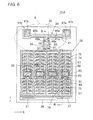
- Fig. 6 is a plan view showing the structure of the electrostatic relay 31A.
- Fig. 7 is a perspective view showing area A of Fig. 6 in an enlarged manner.
- Fig. 8 is a schematic cross-sectional view taken along line B-B of Fig. 6 .
- the electrostatic relay 31A has the fixed contact portion 33, the movable contact portion 34, a fixed electrode portion 35, a movable electrode portion 36 for supporting the movable contact portion 34, an elastic spring 37, and a supporting portion 38 for supporting the elastic spring 37 arranged on the upper surface of the base substrate 32 including the Si substrate, the glass substrate, or the like.
- the fixed contact portion 33 has the lower surface of the fixed contact substrate 41 made of Si fixed to the upper surface of the base substrate 32 by the insulating film 42 (SiO 2 ).
- the insulating layer 43 including an oxide film (SiO 2 ), a nitride film (SiN), or the like is formed on the upper surface of the fixed contact substrate 41, the base layer 44 including the lower layer Cr / upper layer Au is formed on the upper surface thereof, and the conductive layers 45a, 45b of Pt and the like are formed on the base layer 44.
- the fixed contact substrate 41 extends in the width direction (X direction) at the end on the upper surface of the base substrate 32, where a bulging-out portion 41a projecting out towards the movable contact portion 34 side is formed at the central part and pad supporting portions 41 b, 41 b are formed at both ends.
- the conductive layers 45a, 45b are wired along the upper surface of the fixed contact point substrate 41, where one of the ends of the conductive layers 45a, 45b are arranged parallel to each other on the upper surface of the bulging-out portion 41 a, and the distal end faces of the portion projecting out from the end face of the bulging-out portion 41a are positioned within the same plane to become the fixed contacts 46a, 46b (electrical contacting surface), respectively.
- the other ends of the conductive layers 45a, 45b have metal pad portions 47a, 47b formed on the upper surface of the pad supporting portions 41 b, 41 b.
- the movable contact portion 34 is arranged at a position facing the bulging-out portion 41a. As shown in Fig. 8 , the movable contact portion 34 has the insulating layer 53 including the oxide film (SiO 2 ), the nitride film (SiN), or the like formed on the upper surface of the movable contact substrate 51 made of Si, the base layer 54 including the lower layer Cr / upper layer Au formed on the upper surface thereof, and the conductive layer 55 of Pt and the like formed on the base layer 54.
- the end face of the conductive layer 55 facing the conductive layers 45a, 45b projects out from the front surface of the movable contact substrate 41 and is formed parallel to the fixed contact 46a, 46b, whereby the relevant end face becomes the movable contact 56 (electrical contacting surface).
- the movable contact 56 has a width substantially equal to the distance from the edge on the outer side of the fixed contact 46a to the edge on the outer side of the fixed contact 46b.
- the movable contact substrate 51 is supported in a cantilever manner by a supporting beam 57 projecting out from the movable electrode portion 36.
- the lower surfaces of the movable contact substrate 51 and the supporting beam 57 are floating from the upper surface of the base substrate 32, and can move parallel to the length direction (Y direction) of the base substrate 32 with the movable electrode portion 36.
- a main circuit (not shown) is connected to the metal pad portions 47a, 47b of the fixed contact portion 33, where the main circuit can be closed by bringing the movable contact 56 into contact with the fixed contacts 46a, 46b, and the main circuit can be opened by separating the movable contact 56 from the fixed contacts 46a, 46b.
- the opposing surfaces of the bulging-out portion 41a and the movable contact substrate 51 are inclined to retreat towards the lower side, and the fixed contacts 46a, 46b are projected out than the bulging-out portion 41 a and the movable contact 56 is also projected out from the movable contact substrate 51, and hence the bulging-out portion 41 a and the movable contact substrate 51 are not in contact when closing the contacts thereby preventing the movable contact 56 and the fixed contacts 46a, 46b from causing contact failure.
- the actuator for moving the movable contact portion 34 is configured by the fixed electrode portion 35, the movable electrode portion 36, the elastic spring 37, and the supporting portion 38.
- a plurality of fixed electrode portions 35 is arranged in parallel to each other on the upper surface of the base substrate 32.
- the fixed electrode portion 35 has a branch-like electrode part 67 of a branch-shape extending in the Y direction from both surfaces of a rectangular pad portion 66.
- the branch-like electrode part 67 has a branch portion 68 projecting out so as to be symmetrical to each other, the branch portion 68 is lined at a constant pitch in the Y-direction.
- the lower surface of the fixed electrode substrate 61 is fixed to the upper surface of the base substrate 32 by the insulating film 62 in the fixed electrode portion 35.
- the fixed electrode 63 is formed by Cu, Al, and the like on the upper surface of the fixed electrode substrate 61, and an electrode pad layer 65 is arranged above the fixed electrode 63.
- the movable electrode portion 36 is formed to surround each fixed electrode portion 35.
- the movable electrode portion 36 includes a comb teeth like electrode portion 74 formed so as to sandwich each fixed electrode portion 35 from both sides (branch-shape by a pair of comb teeth like electrode portions 74 between the fixed electrode portions 35).
- the comb teeth like electrode portion 74 is symmetric with each fixed electrode portion 35 as the center, where a comb teeth part 75 extends from each comb teeth like electrode portion 74 to a clearance between the branch portions 68.
- each comb teeth part 75 has the distance with the branch portion 68 positioned on the side close to the movable contact portion 34 adjacent to the comb teeth part 75 shorter than the distance with the branch portion 68 positioned on the side distant from the movable contact portion 34 adjacent to the comb teeth part 75.
- the movable electrode portion 36 includes a movable electrode substrate 71 of Si, where the lower surface of the movable electrode substrate 71 is floating from the upper surface of the base substrate 32.
- the supporting beam 57 is arranged in a projecting manner at the center of the end face on the movable contact side of the movable electrode portion 36, and the movable contact portion 34 is held at the distal end of the supporting beam 57.
- the supporting portion 38 is made of Si, and extends long in the X direction at the other end of the base substrate 32.
- the lower surface of the supporting portion 38 is fixed to the upper surface of the base substrate 32 by the insulating film 39.
- Both ends of the supporting portion 38 and the movable electrode portion 36 (movable electrode substrate 71) are connected by a pair of elastic springs 37 formed symmetrically by Si, where the movable electrode portion 36 is horizontally supported by the supporting portion 38 by way of the elastic spring 37.
- the movable electrode portion 36 is movable in the Y direction by elastically deforming the elastic spring 37.
- a DC voltage source is connected between the fixed electrode portion 35 and the movable electrode portion 36, and the DC voltage is turned ON and OFF by the control circuit and the like.
- the fixed electrode portion 35 one terminal of the DC voltage source is connected to the electrode pad layer 65.
- the other terminal of the DC voltage source is connected to the supporting portion 38.
- the supporting portion 38 and the elastic spring 37 have conductivity, and the supporting portion 38, the elastic spring 37, and the movable electrode substrate 71 are electrically conducted, and hence the voltage applied to the supporting portion 38 will be applied to the movable electrode substrate 71.
- each comb teeth part 75 is attracted to the movable contact portion side, and the movable electrode portion 36 moves in the Y direction while bending the elastic spring 37.
- the movable contact portion 34 moves to the fixed contact portion 33 side, and the movable contact 56 come into contact with the fixed contacts 46a, 46b thereby electrically closing the fixed contact 46a and the fixed contact 46b (main circuit).
- Such electrostatic relay 31A is formed through the following steps. First, the Si substrate (another Si wafer having conductivity) is joined to the upper surface of the base substrate 32 (Si wafer, SOl wafer, etc.) having the entire surface covered with the insulating film, and the metal material is vapor deposited on the upper surface of the Si substrate to form the electrode film. The electrode film is then patterned by the photolithography technique, and the fixed electrode 63 is formed on the upper surface of the fixed electrode substrate 61 at the pad portion 66 by the electrode film.
- the insulating layer, the base layer, and the conductive layer are stacked on the upper surface of the Si substrate from above the electrode film.
- the conductive layer is then patterned to form the conductive layers 45a, 45b of the fixed contact portion 33, the conductive layer 55 of the movable contact portion 34, and the electrode pad layer 65 of the fixed electrode portion 35.
- the conductive layers 45a, 45b and the conductive layer 55 are removed through etching leaving the base layer and the insulating layer at the lower surface, where the base layers 44, 54 are formed by the remaining base layer and the insulating layers 43, 53 are formed by the remaining insulating layer.
- the fixed electrode 63, the conductive layers 45a, 45b, and the conductive layer 55 may be simultaneously formed through procedures different from the above.
- a photoresist is applied on the conductive layer 45a, the conductive layer 55, the fixed electrode 63, and the like to form a resist mask, the Si substrate is etched through the resist mask, and the fixed contact substrate 41 of the fixed contact portion 33, the movable contact substrate 51 of the movable contact portion 34, the fixed electrode substrate 61 of the fixed electrode portion 35, the movable electrode substrate 71 of the movable electrode portion 36, the elastic spring 37, and the supporting portion 38 are formed from the Si substrate remaining in each region.
- the insulating film of the region exposed from the Si substrate and the insulating film at the lower surfaces of the movable contact portion 34 and the movable electrode portion 36 are removed through etching, and then cut to individual electrostatic relay 31A.
- the movable contact portion 34 and the fixed electrode portion 35 are formed through steps similar to the steps shown in Fig. 4 or Fig. 5 , and hence the fixed contacts 46a, 46b of the fixed contact portion 33 and the movable contact 56 of the movable contact portion 34 become side surfaces parallel to the growing direction of the conductive layer, and a contact having satisfactory smoothness and parallelism can be obtained without performing polishing and the like. Effects similar to the switch 31 of the first embodiment thus can be obtained in the electrostatic relay 31A as well.
Landscapes
- Chemical & Material Sciences (AREA)
- Engineering & Computer Science (AREA)
- Composite Materials (AREA)
- Materials Engineering (AREA)
- Physics & Mathematics (AREA)
- Electromagnetism (AREA)
- Contacts (AREA)
- Manufacture Of Switches (AREA)
Abstract
A switch (31) and a relay (31A) in which the contacting surface of a contact is smooth are provided. A side surface of a fixed contact portion (33) and a side surface of a movable contact portion (34) face each other. The fixed contact portion (33) has an insulating layer (43) and a base layer (44) stacked on a fixed contact substrate (41), and a conductive layer (45) formed thereon by electrolytic plating, and the like. The side surface of the conductive layer (45) that faces the movable contact portion (34) becomes the fixed contact (46) (contacting surface). The movable contact portion (34) has an insulating layer (53) and a base layer (54) stacked on the movable contact substrate (51), and a movable contact (56) formed thereon by electrolytic plating and the like. The side surface of the conductive layer (55) that faces the fixed contact portion (33) becomes the movable contact (56) (contacting surface). The fixed contact (46) and the movable contact (56) are surfaces being in contact with the side surfaces of the mold portion in the step of growing the conductive layer (45) and the conductive layer (55) by the electrolytic plating, and the like.
Description
- The present invention relates to a switch and a method for manufacturing the same, and a relay. Specifically, the present invention relates to a switch using a metallic contact and a method for manufacturing the same, and also to a relay that uses the structure of the switch.
- A MEMS switch for bringing into contact with and separating from the metallic contact is, for example, disclosed in Japanese Unexamined Patent Publication No.
2006-526267 Fig. 1 , in aswitch 11, aninsulating layer 13a is formed on an upper surface of asubstrate 12a, aconductive layer 14a made of Al, Cu, or the like is formed thereon, and aplated layer 15a of Au or the like is grown from the upper surface to the end face of theconductive layer 14a to form amovable contact portion 17. Similarly, aninsulating layer 13b is formed on an upper surface of asubstrate 12b, aconductive layer 14b made of Al, Cu, or the like is formed thereon, and aplated layer 15b of Au or the like is grown from the upper surface to the end face of theconductive layer 14b to form afixed contact portion 18. A switching operation is carried out between themovable contact portion 17 and thefixed contact portion 18 by moving themovable contact portion 17 in the direction of the arrow, and bringing into contact with or separating from amovable contact 16a that is a projecting region of theplated layer 15a and a fixedcontact 16b that is a projecting region of the platedlayer 15b. - An electrostatic relay is disclosed in Japanese Unexamined Patent Publication No.
9-251834 Fig. 2 , in theelectrostatic relay 21, alever 24a is elastically bent by applying voltage to a movable comb teeth likeelectrode 22a and a fixed comb teeth likeelectrode 23a, and at the same time, alever 24b is elastically bent by applying voltage to a movable comb teeth likeelectrode 22b and a fixed comb teeth likeelectrode 23b, so that amovable contact 25a formed at the distal end of thelever 24a and amovable contact 25b formed at the distal end of thelever 24b are in contact with each other thereby closing between themovable contacts movable contacts electrode electrode electrostatic relay 21, themovable contacts levers - In the
switch 11 of Japanese Unexamined Patent Publication No.2006-526267 movable contact 16a formed at the end face of theconductive layer 14a and the surface of the fixedcontact 16b formed at the end face of theconductive layer 14b is adopted. Therefore, themovable contact 16a and the fixedcontact 16b are in contact with each other at the surfaces (plated surfaces) perpendicular to the growing direction of the plated layer. - In the
electrostatic relay 21 of Japanese Unexamined Patent Publication No.9-251834 movable contacts levers electrostatic relay 21 as well, themovable contacts - However, the surfaces (surfaces of contacts) perpendicular to the growing direction of such contacts are considerably rough when viewed microscopically, and have irregular microscopic bumps. The contacting area of the contacts is thus small when seen microscopically, and the contact resistance in the case where the contacts are closed is large. Furthermore, the contact resistance between the contacts tends to become unnecessarily large since the parallelism of the surfaces of the opposing contacts is difficult to obtain.
- When performing a plating process, the growing speed of the contact is large since the electric field intensity is high at the end face of the conductive layer in the
switch 11 as well as the end face of the lever in theelectrostatic relay 21, and hence, the gap distance between the contacts is difficult to control. Thus, the distance between the contacts becomes difficult to narrow. - A method of smoothing the surface of the contact by polishing and the like is known to resolve such drawbacks, but this increases the polishing step of the contact and becomes a factor in increase in cost of the switch and the relay.
- The present invention has been devised to solve the problems described above, and an object thereof is to provide a switch capable of smoothly forming a contacting surface of a contact without performing polishing, and the like and a method for manufacturing the same, as well as, a relay that uses the structure of the switch.
- In accordance with one aspect of the present invention, a switch according to the present invention relates to a switch including a plurality of contacts that bring into contact with or separate from each other, wherein a surface parallel to a growing direction when forming a conductive layer for forming the contacts is a contacting surface of the contacts.
- In the present invention, the contacting surface of the contact can be formed smooth without performing polishing and the like of the contact since the contacting surfaces of the contacts are surfaces parallel to the growing direction of the conductive layer. The contact resistance in the case where the contacts come into contact with each other thus becomes small. If the contacting surfaces of the contacts are smooth, the contacts come into contact with each other evenly, and hence the contact contacting portion is less likely to break. As a result, the open/dose lifespan of the switch becomes longer, and the distance between the contacts can be narrowed.
- In the one aspect of the switch according to the present invention, the contacting surface of the contact is a surface contacting a mold portion for defining a forming region of the conductive layer when growing the conductive layer. According to such an aspect, the contacting surface of the contact can be formed smooth since the contacting surface of the contact can be formed using the surface of the mold portion.
- In accordance with another aspect of the present invention, a method for manufacturing a switch according to the present invention relates to a method for manufacturing a switch including a plurality of contacts that bring into contact with or separate from each other, the method comprising the steps of forming a mold portion of a predetermined pattern on an upper side of a substrate, growing a conductive layer in a thickness direction of the substrate in a plurality of regions excluding a region formed with the mold portion at the upper side of the substrate, removing the mold portion and having a surface contacting a side surface of the mold portion of the conductive layer as contacting surfaces of the contacts, and dividing the substrate into plurals in accordance with the plurality of regions formed with the conductive layer.
- According to the method for manufacturing the switch of the present invention, the contacting surface of the contact can be formed smooth without performing the polishing and the like of the contact since the contacting surface of the contact can be molded by the side surface of the mold portion when forming the conductive layer. The contact resistance in the case where the contacts come into contact with each other thus becomes small. As the contacting surfaces of the contacts become smooth, the contacting positions of the contacts are dispersed, and the contact contacting portion becomes less likely to break. As a result, the open/dose lifespan of the switch becomes longer, and the distance between the contacts can be narrowed.
- In one aspect of the method for manufacturing the switch according to the present invention, both side surfaces of the mold portion for forming the opposing contacts are formed parallel to each other. According to such an aspect, the contacting surfaces of the contacts can be made parallel to each other.
- In the method for manufacturing the switch according to the present invention, the conductive layer may be grown on the upper side of the substrate through an electrolytic plating or a non-electrolytic plating, or may be grown on the upper side of the substrate through a deposition method such as vapor deposition and sputtering. In the case of the deposition method, the material of the conductive layer deposited on the mold portion can be removed with the mold portion in the step of removing the mold portion.
- A relay according to the present invention includes the switch according to the present invention, and an actuator for moving one part of the contact in a direction perpendicular to the contacting surfaces of the contacts to bring into contact with or separate from the contactseach other. In the relay of the present invention, the contact resistance in the case where the contacts come into contacts with each other can be reduced since the contacting surfaces of the contacts can be formed smooth. If the contacting surfaces of the contacts are smooth, the contacts come into contact with each other evenly, and hence the contact contacting portion is less likely to break. As a result, the lifespan of the relay becomes longer.
- The means for solving the problems in the present invention have characteristics in which the configuring elements described above are appropriately combined, where the present invention includes a great number of variations obtained by combining the configuring elements.
-
-
Fig. 1 is an enlarged cross sectional view of a switch disclosed in Japanese Unexamined Patent Publication No.2006-526267 -
Fig. 2 is a perspective view of an electrostatic relay disclosed in Japanese Unexamined Patent Publication No.9-251834 -
Fig. 3 is a cross-sectional view showing a structure of a switch according to a first embodiment of the present invention; -
Figs. 4A to 4D are schematic cross-sectional views describing the method for manufacturing the switch of the first embodiment; -
Figs. 5A to 5D are schematic cross sectional views describing another method for manufacturing the switch of the first embodiment; -
Fig. 6 is a plan view showing an electrostatic relay according to a second embodiment of the present invention; -
Fig. 7 is a perspective view showing area A ofFig. 6 in an enlarged manner; and -
Fig. 8 is a schematic cross-sectional view taken along line B-B ofFig. 6 . - Hereinafter, preferred embodiments of the present invention will be described with reference to the drawings. The present invention is not limited to the following embodiments, and various design changes can be made within a scope not departing from the gist of the present invention.
-
Fig. 3 is a cross-sectional view showing a structure of a switch according to a first embodiment of the present invention. Theswitch 31 includes afixed contact portion 33 and amovable contact portion 34. Thefixed contact portion 33 is fixed to an upper surface of abase substrate 32 through aninsulating film 42, and themovable contact portion 34 moves in a direction (direction indicated with outlined arrow) parallel to the upper surface of thebase substrate 32 by a drive mechanism or an actuator. For instance, the switch of the present invention can be used in a MEMS switch having the structure dislosed in Japanese Unexamined Patent Publication No.2006-526267 - The fixed
contact portion 33 is obtained by forming an insulating 43 and abase layer 44 on the upper surface of a fixedcontact substrate 41, and forming aconductive layer 45 thereon. Themovable contact portion 34 is obtained by forming an insulating 53 and abase layer 54 on the upper surface of amovable contact substrate 51, and forming aconductive layer 55 thereon. Theconductive layers Fig. 3 ) through electrolytic plating and non-electrolytic plating, vapor deposition, sputtering and the like, where the respective opposing side surfaces become a fixed contact 46 (electrical contacting surface) and a movable contact 56 (electrical contacting surfaces). The material of theconductive layers contact 46 and themovable contact 56 are smoothly formed parallel to each other. Therefore, when themovable contact portion 34 is parallel moved so that the fixedcontact 46 and themovable contact 56 bring into contact with each other to close thecontacts contacts - The opposing portions of the
conductive layer 45 and theconductive layer 55 respectively project out from the end face of the fixedcontact substrate 41 and themovable contact substrate 51, and the opposing surfaces of the fixedcontact substrate 41 and themovable contact substrate 51 are both inclined to retreat toward the lower surface side. Therefore, when moving themovable contact portion 34 to bring contact themovable contact 56 into contact with the fixedcontact 46, the fixedcontact substrate 41 and themovable contact substrate 51 are not in contact with each other thereby inhibiting the contact of themovable contact 56 and the fixedcontact 46. - (First manufacturing method) The
switch 31 is formed using a MEMS (Micro Electrical-Mechanical Systems) technique. The manufacturing method shown inFig. 4A to Fig. 4D forms theconducive layers Fig. 4A shows that in which an insulating layer A3 such as SiO2 and a plated base layer A4 are formed on a substrate A1 made of Si, and a mould portion A2 is formed on the plated base layer A4. The plated base layer A4 becomes a plated electrode and has two-layer structure including the lower layer Cr / upper layer Au, and has the function of enhancing the adhesiveness (stripping strength) of the insulating layer A3 and the conductive layer A5. The mold portion A2 uses a material that has resistance to plating solution and that is selectively etching removed without corroding the conductive layer A5 in the subsequent mold portion removing step. For instance, the mold portion A2 may be formed by exposing a photoresist applied on the upper surface of the plated base layer A4 through an exposure mask, and patterning by etching. Alternatively, the mold portion A2 may be obtained by forming an oxide film (SiO2), a nitride film (SiN), an alumina film (Al2O3), and a metal film of a type different from theconductive layers conductive layers conductive layers Fig. 4A , the entire lower surface of the substrate A1 is fixed to the upper surface of thebase substrate 32 including an Si substrate, a glass substrate, or the like through the insulatingfilm 42 such as the SiO2. - The substrate A1 is then immersed in a plating bath and electrolytic plating is carried out with the plated base layer A4 as the plating electrode, so that the plating metal particles such as Pt gradually precipitate on the surface of the plated base layer A4 and the conductive layer A5 grows in the thickness direction of the substrate A1, as shown in
Fig. 4B . The plating metal particles do not precipitate at the region covered by the mold portion A2. The non-electrolytic plating (chemical plating) may be performed instead of the electrolytic plating. - After cleaning the substrate A1 taken out from the plating bath with water, the mold portion A2 is removed by etching, so that a cavity A6 forms at the area where the mold portion A2 existed between the regions to form the
conductive layers Fig. 4C . One conductive layer A5 separated by the cavity A6 becomes theconductive layer 55, and the side surface facing the cavity A6 becomes themovable contact 56. The other conductive layer A5 separated by the cavity A6 becomes theconductive layer 45, and the side surface facing the cavity A6 becomes the fixedcontact 46. - Then, as shown in
Fig. 4D , etchant is infiltrated from the cavity A6 to sequentially divide the plated base layer A4 and the insulating layer A3 into two. Furthermore, the substrate A1 is etched from the lower surface side or etched from the cavity A6 side to divide into two, where one becomes thebase layer 54, the insulating layer, 53 and themovable contact substrate 51 and the other becomes thebase layer 44, the insulatinglayer 43, and the fixedcontact substrate 41. - One of the blocks thus becomes the
fixed contact portion 33 where the fixedcontact substrate 41, the insulatinglayer 43, thebase layer 44, and theconductive layer 45 are stacked. The fixedcontact portion 33 is fixed to the upper surface of thebase substrate 32 through the insulatingfilm 42. The other block becomes themovable contact portion 34 where themovable contact substrate 51, the insulatinglayer 53, thebase layer 54, and theconductive layer 55 are stacked. Themovable contact portion 34 is separated from thebase substrate 32 by lastly removing the insulating film at the lower surface through etching, whereby the switch 31 (MEMS switch) is formed. - The
switch 31 may be formed through steps shown inFigs. 5A to 5D . This manufacturing method forms theconducive layers Fig. 5A is a step corresponding toFig. 4A , but a adhesion layer A7 (e.g., two-layer structure of lower layer Cr / upper layer Au) for enhancing the adhesion strength (stripping strength) of the insulating layer A3 and the conductive layer A5 is formed in place of the plated base layer A4 on the insulating layer A3. In the step ofFig. 5B , the metal material such as Pt is deposited on the adhesion layer A7 through vapor deposition, sputtering, and the like. The conductive layer A5 is also deposited on the mold portion A2 as shown inFig. 5B according to the deposition method through vapor deposition, sputtering, and the like, but the conductive layer A5 on the mold portion A2 is simultaneously removed when removing the mold portion A2 through etching if the mold portion A2 has sufficient height (lift off method). - The cavity A6 forms after the mold portion A2 is removed as shown in
Fig. 5C , and the conductive layer A5 is separated to theconductive layer 55 and theconductive layer 45, which is the same as the step ofFig. 4C . Furthermore, as shown inFig. 5D , the etchant is infiltrated from the cavity A6 to sequentially divide the adhesion layer A7 and the insulating layer A3 into two, and furthermore, the substrate A1 is divided into two, where one becomes thebase layer 54, the insulating layer, 53 and themovable contact substrate 51 and the other becomes thebase layer 44, the insulatinglayer 43, and the fixedcontact substrate 41, which is the same as the step ofFig. 4D . - In the
switch 31 of the present invention, the contacting surface can be smoothly molded with the side surface of the mold portion without performing polishing and the like since the contacting surface of the fixedcontact 46 and the contacting surface of themovable contact 56 are parallel in the growing direction of the conductive layer A5. The parallelism of the contacting surfaces of thecontacts contacts - Since the accuracy of the gap distance between the
contacts movable contact 56 by the actuator can be reduced. Furthermore, the contacting positions of the contacts are dispersed since the surfaces of the fixedcontact 46 and themovable contact 56 are smooth, and hence the contact contacting portion is less likely to break and the open/close lifespan of theswitch 31 becomes longer. - The structure of the
electrostatic relay 31A for high frequency according to a second embodiment of the present invention will now be described.Fig. 6 is a plan view showing the structure of theelectrostatic relay 31A.Fig. 7 is a perspective view showing area A ofFig. 6 in an enlarged manner.Fig. 8 is a schematic cross-sectional view taken along line B-B ofFig. 6 . - The
electrostatic relay 31A has the fixedcontact portion 33, themovable contact portion 34, a fixedelectrode portion 35, amovable electrode portion 36 for supporting themovable contact portion 34, anelastic spring 37, and a supportingportion 38 for supporting theelastic spring 37 arranged on the upper surface of thebase substrate 32 including the Si substrate, the glass substrate, or the like. - As shown in
Fig. 8 , the fixedcontact portion 33 has the lower surface of the fixedcontact substrate 41 made of Si fixed to the upper surface of thebase substrate 32 by the insulating film 42 (SiO2). The insulatinglayer 43 including an oxide film (SiO2), a nitride film (SiN), or the like is formed on the upper surface of the fixedcontact substrate 41, thebase layer 44 including the lower layer Cr / upper layer Au is formed on the upper surface thereof, and theconductive layers base layer 44. - As shown in
Fig. 6 andFig. 7 , the fixedcontact substrate 41 extends in the width direction (X direction) at the end on the upper surface of thebase substrate 32, where a bulging-out portion 41a projecting out towards themovable contact portion 34 side is formed at the central part and pad supportingportions conductive layers contact point substrate 41, where one of the ends of theconductive layers out portion 41 a, and the distal end faces of the portion projecting out from the end face of the bulging-out portion 41a are positioned within the same plane to become thefixed contacts conductive layers metal pad portions pad supporting portions - The
movable contact portion 34 is arranged at a position facing the bulging-out portion 41a. As shown inFig. 8 , themovable contact portion 34 has the insulatinglayer 53 including the oxide film (SiO2), the nitride film (SiN), or the like formed on the upper surface of themovable contact substrate 51 made of Si, thebase layer 54 including the lower layer Cr / upper layer Au formed on the upper surface thereof, and theconductive layer 55 of Pt and the like formed on thebase layer 54.
The end face of theconductive layer 55 facing theconductive layers movable contact substrate 41 and is formed parallel to the fixedcontact movable contact 56 has a width substantially equal to the distance from the edge on the outer side of the fixedcontact 46a to the edge on the outer side of the fixedcontact 46b. - The
movable contact substrate 51 is supported in a cantilever manner by a supportingbeam 57 projecting out from themovable electrode portion 36. The lower surfaces of themovable contact substrate 51 and the supportingbeam 57 are floating from the upper surface of thebase substrate 32, and can move parallel to the length direction (Y direction) of thebase substrate 32 with themovable electrode portion 36. - In the
electrostatic relay 31A, a main circuit (not shown) is connected to themetal pad portions contact portion 33, where the main circuit can be closed by bringing themovable contact 56 into contact with the fixedcontacts movable contact 56 from the fixedcontacts out portion 41a and themovable contact substrate 51 are inclined to retreat towards the lower side, and the fixedcontacts out portion 41 a and themovable contact 56 is also projected out from themovable contact substrate 51, and hence the bulging-out portion 41 a and themovable contact substrate 51 are not in contact when closing the contacts thereby preventing themovable contact 56 and the fixedcontacts - The actuator for moving the
movable contact portion 34 is configured by the fixedelectrode portion 35, themovable electrode portion 36, theelastic spring 37, and the supportingportion 38. - As shown in
Fig. 6 , a plurality of fixedelectrode portions 35 is arranged in parallel to each other on the upper surface of thebase substrate 32. In plan view, the fixedelectrode portion 35 has a branch-like electrode part 67 of a branch-shape extending in the Y direction from both surfaces of arectangular pad portion 66. The branch-like electrode part 67 has abranch portion 68 projecting out so as to be symmetrical to each other, thebranch portion 68 is lined at a constant pitch in the Y-direction. - As shown in
Fig. 8 , the lower surface of the fixedelectrode substrate 61 is fixed to the upper surface of thebase substrate 32 by the insulatingfilm 62 in the fixedelectrode portion 35. In thepad portion 66, the fixedelectrode 63 is formed by Cu, Al, and the like on the upper surface of the fixedelectrode substrate 61, and anelectrode pad layer 65 is arranged above the fixedelectrode 63. - As shown in
Fig. 6 , themovable electrode portion 36 is formed to surround each fixedelectrode portion 35. Themovable electrode portion 36 includes a comb teeth likeelectrode portion 74 formed so as to sandwich each fixedelectrode portion 35 from both sides (branch-shape by a pair of comb teeth likeelectrode portions 74 between the fixed electrode portions 35). The comb teeth likeelectrode portion 74 is symmetric with each fixedelectrode portion 35 as the center, where acomb teeth part 75 extends from each comb teeth likeelectrode portion 74 to a clearance between thebranch portions 68. Furthermore, eachcomb teeth part 75 has the distance with thebranch portion 68 positioned on the side close to themovable contact portion 34 adjacent to thecomb teeth part 75 shorter than the distance with thebranch portion 68 positioned on the side distant from themovable contact portion 34 adjacent to thecomb teeth part 75. - The
movable electrode portion 36 includes amovable electrode substrate 71 of Si, where the lower surface of themovable electrode substrate 71 is floating from the upper surface of thebase substrate 32. The supportingbeam 57 is arranged in a projecting manner at the center of the end face on the movable contact side of themovable electrode portion 36, and themovable contact portion 34 is held at the distal end of the supportingbeam 57. - The supporting
portion 38 is made of Si, and extends long in the X direction at the other end of thebase substrate 32. The lower surface of the supportingportion 38 is fixed to the upper surface of thebase substrate 32 by the insulatingfilm 39. Both ends of the supportingportion 38 and the movable electrode portion 36 (movable electrode substrate 71) are connected by a pair ofelastic springs 37 formed symmetrically by Si, where themovable electrode portion 36 is horizontally supported by the supportingportion 38 by way of theelastic spring 37. Themovable electrode portion 36 is movable in the Y direction by elastically deforming theelastic spring 37. - In the
electrostatic relay 31A having the above structure, a DC voltage source is connected between the fixedelectrode portion 35 and themovable electrode portion 36, and the DC voltage is turned ON and OFF by the control circuit and the like. In the fixedelectrode portion 35, one terminal of the DC voltage source is connected to theelectrode pad layer 65. The other terminal of the DC voltage source is connected to the supportingportion 38. The supportingportion 38 and theelastic spring 37 have conductivity, and the supportingportion 38, theelastic spring 37, and themovable electrode substrate 71 are electrically conducted, and hence the voltage applied to the supportingportion 38 will be applied to themovable electrode substrate 71. - When the DC voltage is applied between the fixed
electrode portion 35 and themovable electrode portion 36 by the DC voltage source, an electrostatic attractive force is generated between thebranch portion 68 of the branch likeelectrode part 67 and thecomb teeth part 75 of the comb teeth likeelectrode portion 74. However, the electrostatic attractive force in the X direction acting on themovable electrode portion 36 becomes balanced since the structure of the fixedelectrode portion 35 and themovable electrode portion 36 is formed symmetric with respect to the center line of each fixedelectrode portion 35, whereby themoveable electrode portion 36 does not move in the X direction. Since the distance with thebranch portion 68 positioned on the side close to themovable contact portion 34 adjacent to thecomb teeth part 75 is shorter than the distance with thebranch portion 68 positioned on the side distant from themovable contact portion 34 adjacent to thecomb teeth part 75, eachcomb teeth part 75 is attracted to the movable contact portion side, and themovable electrode portion 36 moves in the Y direction while bending theelastic spring 37. As a result, themovable contact portion 34 moves to the fixedcontact portion 33 side, and themovable contact 56 come into contact with the fixedcontacts fixed contact 46a and the fixedcontact 46b (main circuit). - When the DC voltage applied between the fixed
electrode portion 35 and themovable electrode portion 36 is released, the electrostatic attractive force between thebranch portion 68 and thecomb teeth part 35 disappears, whereby themovable electrode portion 36 moves backward in the Y direction by the elastic returning force of the elastic spring 47 thereby separating themovable contact 56 from the fixedcontacts contact 46a and the fixedcontact 46b (main circuit). - Such
electrostatic relay 31A is formed through the following steps. First, the Si substrate (another Si wafer having conductivity) is joined to the upper surface of the base substrate 32 (Si wafer, SOl wafer, etc.) having the entire surface covered with the insulating film, and the metal material is vapor deposited on the upper surface of the Si substrate to form the electrode film. The electrode film is then patterned by the photolithography technique, and the fixedelectrode 63 is formed on the upper surface of the fixedelectrode substrate 61 at thepad portion 66 by the electrode film. - Thereafter, the insulating layer, the base layer, and the conductive layer are stacked on the upper surface of the Si substrate from above the electrode film. The conductive layer is then patterned to form the
conductive layers contact portion 33, theconductive layer 55 of themovable contact portion 34, and theelectrode pad layer 65 of the fixedelectrode portion 35. Theconductive layers conductive layer 55 are removed through etching leaving the base layer and the insulating layer at the lower surface, where the base layers 44, 54 are formed by the remaining base layer and the insulatinglayers - The fixed
electrode 63, theconductive layers conductive layer 55 may be simultaneously formed through procedures different from the above. - Thereafter, a photoresist is applied on the
conductive layer 45a, theconductive layer 55, the fixedelectrode 63, and the like to form a resist mask, the Si substrate is etched through the resist mask, and the fixedcontact substrate 41 of the fixedcontact portion 33, themovable contact substrate 51 of themovable contact portion 34, the fixedelectrode substrate 61 of the fixedelectrode portion 35, themovable electrode substrate 71 of themovable electrode portion 36, theelastic spring 37, and the supportingportion 38 are formed from the Si substrate remaining in each region. - Lastly, the insulating film of the region exposed from the Si substrate and the insulating film at the lower surfaces of the
movable contact portion 34 and themovable electrode portion 36 are removed through etching, and then cut to individualelectrostatic relay 31A. - In the manufacturing step of the
electrostatic relay 31A, themovable contact portion 34 and the fixedelectrode portion 35 are formed through steps similar to the steps shown inFig. 4 orFig. 5 , and hence the fixedcontacts contact portion 33 and themovable contact 56 of themovable contact portion 34 become side surfaces parallel to the growing direction of the conductive layer, and a contact having satisfactory smoothness and parallelism can be obtained without performing polishing and the like. Effects similar to theswitch 31 of the first embodiment thus can be obtained in theelectrostatic relay 31A as well.
Claims (8)
- A switch (31) including a plurality of contacts that bring into contact with or separate from each other, characterized in that:a surface parallel to a growing direction when forming a conductive layer (45, 45a, 45b, 55) for forming the contacts is a contacting surface of the contacts.
- The switch (31) according to claim 1, characterized in that:the contacting surface of the contact is a surface contacting a mold portion for defining a forming region of the conductive layer (45, 45a, 45b, 55) when growing the conductive layer (45, 45a, 45b, 55)
- A method for manufacturing a switch including a plurality of contacts that bring into contact with or separate from each other,
the method being characterized by comprising the steps of:forming a mold portion of a predetermined pattern on an upper side of a substrate,growing a conductive layer (45, 45a, 45b, 55) in a thickness direction of the substrate in a plurality of regions excluding a region formed with the mold portion at the upper side of the substrate,removing the mold portion and having a surface contacting a side surface of the mold portion of the conductive layer (45, 45a, 45b, 55) as contacting surfaces of the contacts, anddividing the substrate into plurals in accordance with the plurality of regions formed with the conductive layer (45, 45a, 45b, 55). - The method for manufacturing the switch (31) according to claim 3, characterized in that:both side surfaces of the mold portion for forming the opposing contacts are formed parallel to each other.
- The method for manufacturing the switch (31) according to claim 3, characterized in that:the conductive layer (45, 45a, 45b, 55) is grown on the upper side of the substrate through an electrolytic plating or a non-electrolytic plating.
- The method for manufacturing the switch (31) according to claim 3, characterized in that:the conducive layer (45, 45a, 45b, 55) is grown on the upper side of the substrate through a deposition method such as vapor deposition and sputtering.
- The method for manufacturing the switch (31) according to claim 6, characterized in that:the material of the conductive layer (45, 45a, 45b, 55) deposited on the mold portion is removed with the mold portion in the step of removing the mold portion.
- A relay (31A) being characterized by comprising:the switch (31) according to claim 1, andan actuator for moving one part of the contact in a direction perpendicular to the contacting surfaces of the contacts to bring into contact with or separate from the contacts each other.
Applications Claiming Priority (1)
| Application Number | Priority Date | Filing Date | Title |
|---|---|---|---|
| JP2010043899A JP5187327B2 (en) | 2010-03-01 | 2010-03-01 | Switch, manufacturing method thereof, and relay |
Publications (1)
| Publication Number | Publication Date |
|---|---|
| EP2365498A1 true EP2365498A1 (en) | 2011-09-14 |
Family
ID=44070065
Family Applications (1)
| Application Number | Title | Priority Date | Filing Date |
|---|---|---|---|
| EP11151193A Withdrawn EP2365498A1 (en) | 2010-03-01 | 2011-01-18 | Switch and method for manufacturing the same, and relay |
Country Status (2)
| Country | Link |
|---|---|
| EP (1) | EP2365498A1 (en) |
| JP (1) | JP5187327B2 (en) |
Cited By (4)
| Publication number | Priority date | Publication date | Assignee | Title |
|---|---|---|---|---|
| FR3034567A1 (en) * | 2015-03-31 | 2016-10-07 | Stmicroelectronics Rousset | METALLIC DEVICE WITH IMPROVED MOBILE PIECE (S) LODGED IN A CAVITY OF THE INTERCONNECTION PART ("BEOL") OF AN INTEGRATED CIRCUIT |
| US9466452B1 (en) | 2015-03-31 | 2016-10-11 | Stmicroelectronics, Inc. | Integrated cantilever switch |
| CN107077999A (en) * | 2014-09-26 | 2017-08-18 | 索尼公司 | Switchgear and Electronics |
| DE102021203566A1 (en) | 2021-04-12 | 2022-10-13 | Robert Bosch Gesellschaft mit beschränkter Haftung | MEMS switch with embedded metal contact |
Families Citing this family (1)
| Publication number | Priority date | Publication date | Assignee | Title |
|---|---|---|---|---|
| EP3378080B1 (en) | 2015-11-16 | 2022-11-23 | Qorvo US, Inc. | Mems device and method for fabricating a mems device |
Citations (4)
| Publication number | Priority date | Publication date | Assignee | Title |
|---|---|---|---|---|
| JPH09251834A (en) | 1996-03-15 | 1997-09-22 | Omron Corp | Electrostatic relay |
| DE19935678A1 (en) * | 1999-07-29 | 2001-02-01 | Bosch Gmbh Robert | Relay has contacts, spring element, actuating element formed by mechanical microstructures electrically connected to upper side of bearer substrate and in plane parallel to substrate upper side |
| US20020184949A1 (en) * | 2001-06-04 | 2002-12-12 | Gianchandani Yogesh B. | Micromachined shock sensor |
| JP2006526267A (en) | 2003-04-29 | 2006-11-16 | メドトロニック・インコーポレーテッド | Multi-stable microelectromechanical switch switch and manufacturing method thereof |
Family Cites Families (1)
| Publication number | Priority date | Publication date | Assignee | Title |
|---|---|---|---|---|
| JPH08264090A (en) * | 1995-03-24 | 1996-10-11 | Nippon Telegr & Teleph Corp <Ntt> | Wiring breaker and manufacturing method |
-
2010
- 2010-03-01 JP JP2010043899A patent/JP5187327B2/en not_active Expired - Fee Related
-
2011
- 2011-01-18 EP EP11151193A patent/EP2365498A1/en not_active Withdrawn
Patent Citations (4)
| Publication number | Priority date | Publication date | Assignee | Title |
|---|---|---|---|---|
| JPH09251834A (en) | 1996-03-15 | 1997-09-22 | Omron Corp | Electrostatic relay |
| DE19935678A1 (en) * | 1999-07-29 | 2001-02-01 | Bosch Gmbh Robert | Relay has contacts, spring element, actuating element formed by mechanical microstructures electrically connected to upper side of bearer substrate and in plane parallel to substrate upper side |
| US20020184949A1 (en) * | 2001-06-04 | 2002-12-12 | Gianchandani Yogesh B. | Micromachined shock sensor |
| JP2006526267A (en) | 2003-04-29 | 2006-11-16 | メドトロニック・インコーポレーテッド | Multi-stable microelectromechanical switch switch and manufacturing method thereof |
Non-Patent Citations (2)
| Title |
|---|
| GUCKEL H: "High-Aspect-Ratio Micromachining Via Deep X-Ray Lithography", PROCEEDINGS OF THE IEEE, IEEE. NEW YORK, US, vol. 86, no. 8, 1 August 1998 (1998-08-01), pages 1586 - 1593, XP011044068, ISSN: 0018-9219, DOI: 10.1109/5.704264 * |
| ROY S ET AL: "DESIGN, FABRICATION, AND CHRACTERIZATION OF ELECTROSTATIC MICRORELAYS", PROCEEDINGS OF SPIE, S P I E - INTERNATIONAL SOCIETY FOR OPTICAL ENGINEERING, US, vol. 2642, 1 January 1995 (1995-01-01), pages 64 - 73, XP000783558, ISSN: 0277-786X, DOI: 10.1117/12.221184 * |
Cited By (10)
| Publication number | Priority date | Publication date | Assignee | Title |
|---|---|---|---|---|
| CN107077999A (en) * | 2014-09-26 | 2017-08-18 | 索尼公司 | Switchgear and Electronics |
| CN107077999B (en) * | 2014-09-26 | 2019-05-31 | 索尼公司 | Switchgear and Electronic Equipment |
| FR3034567A1 (en) * | 2015-03-31 | 2016-10-07 | Stmicroelectronics Rousset | METALLIC DEVICE WITH IMPROVED MOBILE PIECE (S) LODGED IN A CAVITY OF THE INTERCONNECTION PART ("BEOL") OF AN INTEGRATED CIRCUIT |
| US9466452B1 (en) | 2015-03-31 | 2016-10-11 | Stmicroelectronics, Inc. | Integrated cantilever switch |
| US9653392B2 (en) | 2015-03-31 | 2017-05-16 | Stmicroelectronics (Rousset) Sas | Metallic device having mobile element in a cavity of the BEOL of an integrated circuit |
| US9875870B2 (en) | 2015-03-31 | 2018-01-23 | Stmicroelectronics (Rousset) Sas | Metallic device having mobile element in a cavity of the BEOL of an integrated circuit |
| US9905706B2 (en) | 2015-03-31 | 2018-02-27 | Stmicroelectronics, Inc. | Integrated cantilever switch |
| US10861984B2 (en) | 2015-03-31 | 2020-12-08 | Stmicroelectronics, Inc. | Integrated cantilever switch |
| DE102021203566A1 (en) | 2021-04-12 | 2022-10-13 | Robert Bosch Gesellschaft mit beschränkter Haftung | MEMS switch with embedded metal contact |
| US12230457B2 (en) | 2021-04-12 | 2025-02-18 | Robert Bosch Gmbh | Method for manufacturing a MEMS switch having an embedded metal contact |
Also Published As
| Publication number | Publication date |
|---|---|
| JP2011181315A (en) | 2011-09-15 |
| JP5187327B2 (en) | 2013-04-24 |
Similar Documents
| Publication | Publication Date | Title |
|---|---|---|
| JP5131298B2 (en) | Switch, manufacturing method thereof, and electrostatic relay | |
| EP2365498A1 (en) | Switch and method for manufacturing the same, and relay | |
| EP2365509B1 (en) | Electrostatic relay | |
| US20140034465A1 (en) | Switch and method for manufacturing the same, and relay | |
| WO2008045230A9 (en) | Contact electrode for microdevices and etch method of manufacture | |
| US7464459B1 (en) | Method of forming a MEMS actuator and relay with vertical actuation | |
| US7902946B2 (en) | MEMS relay with a flux path that is decoupled from an electrical path through the switch and a suspension structure that is independent of the core structure and a method of forming the same | |
| JP2009009884A (en) | MEMS switch and manufacturing method thereof | |
| EP2365499A1 (en) | Switch and method for manufacturing the same, and relay | |
| US7965159B2 (en) | Micro-switching device and manufacturing method for the same | |
| WO2007060416A1 (en) | A micro-electromechanical device and method of making the same | |
| CN103858199B (en) | Electrical equipment with movable part and its manufacture method | |
| JP4292532B2 (en) | Mechanism device manufacturing method, mechanism device, and micro reed switch | |
| US7601554B1 (en) | Shaped MEMS contact | |
| KR100513716B1 (en) | Manufacturing method of Self alligning membrance | |
| JP2005504415A (en) | Micromechanical switch and method of manufacturing the same | |
| JPH0714483A (en) | Micro bimetal relay and manufacturing method thereof | |
| JP2003242850A (en) | Contact for electric switch, method for manufacturing the same, and electric switch | |
| CN102543522A (en) | Method for manufacturing a micro-contactor that can be actuated by a magnetic field | |
| JP2012038661A (en) | Mems switch and method of manufacturing mems switch | |
| JP2004261949A (en) | Method for forming microstructure, microstructure and optical switch | |
| JP2001210206A (en) | Thermo switch and method for manufacturing the same |
Legal Events
| Date | Code | Title | Description |
|---|---|---|---|
| PUAI | Public reference made under article 153(3) epc to a published international application that has entered the european phase |
Free format text: ORIGINAL CODE: 0009012 |
|
| AK | Designated contracting states |
Kind code of ref document: A1 Designated state(s): AL AT BE BG CH CY CZ DE DK EE ES FI FR GB GR HR HU IE IS IT LI LT LU LV MC MK MT NL NO PL PT RO RS SE SI SK SM TR |
|
| AX | Request for extension of the european patent |
Extension state: BA ME |
|
| 17P | Request for examination filed |
Effective date: 20120209 |
|
| 17Q | First examination report despatched |
Effective date: 20140821 |
|
| STAA | Information on the status of an ep patent application or granted ep patent |
Free format text: STATUS: THE APPLICATION IS DEEMED TO BE WITHDRAWN |
|
| 18D | Application deemed to be withdrawn |
Effective date: 20150102 |