EP2365385A1 - Liquid crystal display with improved bonding strength between the sealant and the substrate - Google Patents
Liquid crystal display with improved bonding strength between the sealant and the substrate Download PDFInfo
- Publication number
- EP2365385A1 EP2365385A1 EP11153624A EP11153624A EP2365385A1 EP 2365385 A1 EP2365385 A1 EP 2365385A1 EP 11153624 A EP11153624 A EP 11153624A EP 11153624 A EP11153624 A EP 11153624A EP 2365385 A1 EP2365385 A1 EP 2365385A1
- Authority
- EP
- European Patent Office
- Prior art keywords
- liquid crystal
- substrate
- crystal display
- sealant
- holes
- Prior art date
- Legal status (The legal status is an assumption and is not a legal conclusion. Google has not performed a legal analysis and makes no representation as to the accuracy of the status listed.)
- Withdrawn
Links
- 239000000758 substrate Substances 0.000 title claims abstract description 67
- 239000004973 liquid crystal related substance Substances 0.000 title claims abstract description 45
- 239000000565 sealant Substances 0.000 title claims abstract description 33
- 239000010409 thin film Substances 0.000 claims description 5
- 230000001788 irregular Effects 0.000 claims 1
- 238000007789 sealing Methods 0.000 abstract description 4
- 238000000034 method Methods 0.000 description 4
- 239000011248 coating agent Substances 0.000 description 2
- 238000000576 coating method Methods 0.000 description 2
- 230000007547 defect Effects 0.000 description 2
- 239000011159 matrix material Substances 0.000 description 2
- 239000012780 transparent material Substances 0.000 description 2
- 239000004593 Epoxy Substances 0.000 description 1
- ISWSIDIOOBJBQZ-UHFFFAOYSA-N Phenol Chemical compound OC1=CC=CC=C1 ISWSIDIOOBJBQZ-UHFFFAOYSA-N 0.000 description 1
- 239000000463 material Substances 0.000 description 1
- 238000000059 patterning Methods 0.000 description 1
- 239000011347 resin Substances 0.000 description 1
- 229920005989 resin Polymers 0.000 description 1
Images


Classifications
-
- G—PHYSICS
- G02—OPTICS
- G02F—OPTICAL DEVICES OR ARRANGEMENTS FOR THE CONTROL OF LIGHT BY MODIFICATION OF THE OPTICAL PROPERTIES OF THE MEDIA OF THE ELEMENTS INVOLVED THEREIN; NON-LINEAR OPTICS; FREQUENCY-CHANGING OF LIGHT; OPTICAL LOGIC ELEMENTS; OPTICAL ANALOGUE/DIGITAL CONVERTERS
- G02F1/00—Devices or arrangements for the control of the intensity, colour, phase, polarisation or direction of light arriving from an independent light source, e.g. switching, gating or modulating; Non-linear optics
- G02F1/01—Devices or arrangements for the control of the intensity, colour, phase, polarisation or direction of light arriving from an independent light source, e.g. switching, gating or modulating; Non-linear optics for the control of the intensity, phase, polarisation or colour
- G02F1/13—Devices or arrangements for the control of the intensity, colour, phase, polarisation or direction of light arriving from an independent light source, e.g. switching, gating or modulating; Non-linear optics for the control of the intensity, phase, polarisation or colour based on liquid crystals, e.g. single liquid crystal display cells
- G02F1/133—Constructional arrangements; Operation of liquid crystal cells; Circuit arrangements
- G02F1/1333—Constructional arrangements; Manufacturing methods
- G02F1/1339—Gaskets; Spacers; Sealing of cells
-
- G—PHYSICS
- G02—OPTICS
- G02F—OPTICAL DEVICES OR ARRANGEMENTS FOR THE CONTROL OF LIGHT BY MODIFICATION OF THE OPTICAL PROPERTIES OF THE MEDIA OF THE ELEMENTS INVOLVED THEREIN; NON-LINEAR OPTICS; FREQUENCY-CHANGING OF LIGHT; OPTICAL LOGIC ELEMENTS; OPTICAL ANALOGUE/DIGITAL CONVERTERS
- G02F1/00—Devices or arrangements for the control of the intensity, colour, phase, polarisation or direction of light arriving from an independent light source, e.g. switching, gating or modulating; Non-linear optics
- G02F1/01—Devices or arrangements for the control of the intensity, colour, phase, polarisation or direction of light arriving from an independent light source, e.g. switching, gating or modulating; Non-linear optics for the control of the intensity, phase, polarisation or colour
- G02F1/13—Devices or arrangements for the control of the intensity, colour, phase, polarisation or direction of light arriving from an independent light source, e.g. switching, gating or modulating; Non-linear optics for the control of the intensity, phase, polarisation or colour based on liquid crystals, e.g. single liquid crystal display cells
- G02F1/133—Constructional arrangements; Operation of liquid crystal cells; Circuit arrangements
- G02F1/1333—Constructional arrangements; Manufacturing methods
- G02F1/1337—Surface-induced orientation of the liquid crystal molecules, e.g. by alignment layers
- G02F1/13378—Surface-induced orientation of the liquid crystal molecules, e.g. by alignment layers by treatment of the surface, e.g. embossing, rubbing or light irradiation
- G02F1/133784—Surface-induced orientation of the liquid crystal molecules, e.g. by alignment layers by treatment of the surface, e.g. embossing, rubbing or light irradiation by rubbing
Definitions
- the present invention relates to a liquid crystal display device, particularly but not exclusively to a liquid crystal display device in which bonding force between a sealant and a substrate is improved.
- a liquid crystal display (LCD) using an electro-optic property of a liquid crystal to display an image or text is widely used in view of excellent colour reproduction, low power consumption, and because the LCD can be manufactured to be thin.
- the LCD includes a display panel displaying an image and text, a drive integrated circuit (IC) driving the display panel, and a backlight unit providing light to the display panel.
- IC drive integrated circuit
- the display panel includes a lower substrate on which a pixel electrode is formed, an upper substrate on which a common electrode is formed, a liquid crystal layer disposed between the pixel electrode and the common electrode.
- the liquid crystal layer is sealed by a sealant formed along an edge between the lower substrate and the upper substrate to seal a space between the pixel electrode and the common electrode.
- the sealant is formed in a non-pixel region around the pixel region.
- aspects of the present invention provide a liquid crystal display being minimized by reducing a size of a non-pixel region.
- aspects of the present invention provide a liquid crystal display for maintaining a stable sealing state with a small area by improving a bonding force between a sealant and a substrate.
- a liquid crystal display comprising a first substrate including a first electrode and a first orientation layer, a second substrate facing the first substrate and including a second electrode and a second orientation layer, a sealant formed along edges of the first substrate and the second substrate and a liquid crystal layer between the first electrode and the second electrode, wherein the sealant is in contact with one or both of the first and second substrates through holes in one or both of the first and second orientation layers.
- a liquid crystal display which includes a first substrate on which a first electrode and a first orientation layer are formed; a second substrate facing the first substrate and including a second electrode and a second orientation layer; a sealant formed along edges of the first substrate and the second substrate; and a liquid crystal layer between the first electrode and the second electrode; wherein holes are formed in the first and second orientation layers and the sealant is bonded to the first and second subatrates through both side holes.
- the orientation layer is disposed between the sealant and the substrate and the holes are formed in the first orientation layer and the second orientation layer between the sealant and the first substrate and the second substrate so that the sealant is bonded to the first substrate and the second substrate through the holes. Since a contact area between the sealant and the first substrate and the second substrate is increased and the bonding force is improved, a stable sealing state can be maintained with a small area. The size of the non-pixel region is effectively reduced so that a small liquid crystal display can be achieved.
- first element is said to be disposed or formed “on” or “in” or “connected to” a second element
- first element can directly contact the second element, or can be separated from the second element by one or more other elements located therebetween.
- an element is referred to as being disposed or formed "directly on” or “directly connected to” another element, there are no intervening elements present.
- FIG. 1 is a perspective view illustrating a liquid crystal display according to an embodiment of the present invention.
- FIG. 2 is a schematic perspective view illustrating a pixel region P of FIG. 1 .
- a liquid crystal display (LCD) 100 includes a lower substrate 110 and an upper substrate 120 that are disposed to face each other, and a liquid crystal layer 130 disposed between the lower substrate 110 and the upper substrate 120.
- the lower substrate 110 includes a pixel region P and a non-pixel region D around the pixel region P.
- a plurality of gate lines 111 and data lines 112 are arranged in the form of matrix on the lower substrate 110 in the pixel region P. Pixels are defined by the gate lines 111 and the data lines 112 intersecting each other.
- Thin film transistors 114 control signals supplied to the respective pixels and pixel electrodes 115 connected to the thin film transistors 114.
- the thin film transistors 114 are made of a transparent material and are formed at portions where the gate lines 111 intersect the data lines 112.
- a pad unit 150 receiving a signal from the outside and a drive IC 140 driving the liquid crystal are mounted on the lower substrate 110 in the non-pixel region D.
- the drive IC 140 processes an electric signal provided from the outside through the pad unit 150 and provides the processed signal to the gate lines 111 and the data lines 112.
- the lower substrate 110 and the upper substrate 120 are disposed to face each other and are bonded to each other by a sealant 160.
- a liquid crystal layer 130 is injected into a space sealed between the lower substrate 110 and the upper substrate 120.
- the liquid crystal layer 130 is disposed in the space between one of the pixel electrodes 115 and the common electrode 123 and is sealed by a sealant 160 along edges of the lower substrate 110 and the upper substrate 120.
- the sealant 160 is made of resin such as epoxy, phenol, and is formed in the non-pixel region to surround the pixel region P.
- the sealant 160 may be formed of other suitable materials.
- polarizers are installed at the rear sides of the lower substrate 110, the upper substrate 120 and a back light unit (not shown) as a light source is disposed at the rear side of the lower substrate 110. Therefore, light provided from the back light (not shown) enters the liquid crystal layer 130, is modulated by the liquid crystal oriented by voltages applied to the pixel electrode 115 and the common electrode 123, and is emitted to the outside through the upper substrate 120 to display text and an image.
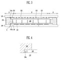
- FIG. 3 is a sectional view taken along the line I1-I2 of FIG. 1 .
- FIG. 4 is an enlarged sectional view of an "X" portion of FIG. 3 .
- the embodiments of the present invention will be described in detail with reference to FIGs. 3 and 4 .
- the liquid crystal layer 130 is disposed between an orientation layer 116 formed on the pixel electrode 115 and an orientation layer 124 formed on the common electrode 123.
- the orientation layers 116 and 124 are rubbed such that a pretilt angle and an orientation of liquid crystal molecules are adjusted after coating. Since the pretilt angle and the orientation of liquid crystal molecules are adjusted, defects, such as light leakage, occur in the orientation layers 116 and 124 when the orientation layers 116 and 124 are not formed in the pixel region P. Therefore, the orientation layers 116 and 124 are coated to be wider than the pixel region P. In other words, the orientation layers 116 and 125 are coated to include a whole of the pixel region P and some of the non-pixel region D by considering the process margin.
- the embodiments of the present invention coat and rub the orientation layers 116 and 124 and form holes 116a and 124a in the orientation layers 116 and 124 coated in the non-pixel region D. That, as illustrated in FIG. 4 , the sealant 160 contacts the substrates 110 and 120 through the holes 116a and 124a formed on the orientation layers 116 and 124 so that the contact area between the sealant 160 and the substrates 110 and 120 is increased and the bonding force can be improved.
- the size of the non-pixel region D is determined by a wire, an area occupied by the pad unit 150 and the drive IC 140, the process margin when coating the orientation layers 116 and 124, the contact area between the sealant 160 and the substrates 110 and 120, and a cutting margin separating a unit display panel are reduced and the size of the non-pixel region D can be effectively reduced.
- a stable sealing state can be maintained with a small area due to the improved bonding force between the sealant 160 and the substrates 110 and 120.
- FIGs. 5 and 6 are layout views illustrating the orientation layers 116 and 126 and the sealant 160.
- the holes 116a and 124a of the orientation layers 116 and 124 are rectangular or circular and are arranged alternately. However, aspects of the present invention are not limited thereto, and the holes 116a and 124a may have other suitable shapes and be arranged in other suitable manners.
- the size of the holes 116a and 124a is smaller than the size of a unit pixel and an area occupied by overall holes 116a and 124a is 20 to 50% of a contact area with the sealant 160.
- the orientation layers 116 and 124 are 700nm, defects may be prevented during the patterning when the holes 116a and 124a are a few micrometers to a few tens of micrometers.
- FIGs. 5 and 6 illustrate a regular arrangement of the holes 116a and 124a, the holes 116a and 124a may be arranged irregularly to prevent light leakage from concentrating on a specific pixel.
- FIG. 5 illustrates the orientation layers 116 and 124 formed in the whole of the pixel region P and some of the non-pixel region D.
- the sealant 160 contacts the substrates 110 and 120 through the holes 116a and 124a of orientation layers 116 and 124.
- FIG. 6 illustrates the holes 116a and 124a of the orientation layers 116 and 124 positioned in the pixel region P, rather than the non-pixel region D, due to a process error.
- the holes 116a and 124a are arranged alternately and are smaller than the size of a unit pixel, the orientation of the liquid crystal layer 130 is not affected. That is, since another hole is not disposed around one of the holes 116a and 124a, the liquid crystal molecules are oriented by the orientation layers 116 and 124 around the holes 116a and 124a.
Landscapes
- Physics & Mathematics (AREA)
- Nonlinear Science (AREA)
- Mathematical Physics (AREA)
- Chemical & Material Sciences (AREA)
- Crystallography & Structural Chemistry (AREA)
- General Physics & Mathematics (AREA)
- Optics & Photonics (AREA)
- Spectroscopy & Molecular Physics (AREA)
- Liquid Crystal (AREA)
Abstract
A liquid crystal display including: a first substrate (110) on which a first electrode (115) and a first orientation layer (116) are formed; a second substrate (120) facing the first substrate (110) and including a second electrode (123) and a second orientation layer (124); a sealant (160) formed along edges of the first substrate (110) and the second substrate (120); and a liquid crystal layer (130) between the first electrode (115) and the second electrode (123); wherein holes (116a,124a) are formed in the first and/or second orientation layers (116,124) and the sealant (160) is bonded to the first and/or second substrates (110,120) through the holes (116a,124a). Since a contact area between the sealant (160) and the substrates (110,120) is increased and a bonding force is improved, a stable sealing state can be maintained with a small area and a size of a non-pixel region (D) is reduced so that a small-sized liquid crystal display can be achieved.
Description
- The present invention relates to a liquid crystal display device, particularly but not exclusively to a liquid crystal display device in which bonding force between a sealant and a substrate is improved.
- A liquid crystal display (LCD) using an electro-optic property of a liquid crystal to display an image or text is widely used in view of excellent colour reproduction, low power consumption, and because the LCD can be manufactured to be thin. The LCD includes a display panel displaying an image and text, a drive integrated circuit (IC) driving the display panel, and a backlight unit providing light to the display panel.
- The display panel includes a lower substrate on which a pixel electrode is formed, an upper substrate on which a common electrode is formed, a liquid crystal layer disposed between the pixel electrode and the common electrode. The liquid crystal layer is sealed by a sealant formed along an edge between the lower substrate and the upper substrate to seal a space between the pixel electrode and the common electrode. The sealant is formed in a non-pixel region around the pixel region. Recently, displays have become smaller according to user requirements. However, there are problems when reducing a size of the pixel region, so, research on minimizing a size of the non-pixel region is conducted in order to reduce the display size.
- Aspects of the present invention provide a liquid crystal display being minimized by reducing a size of a non-pixel region.
- Aspects of the present invention provide a liquid crystal display for maintaining a stable sealing state with a small area by improving a bonding force between a sealant and a substrate.
- According to an aspect of the invention, there is provided a liquid crystal display comprising a first substrate including a first electrode and a first orientation layer, a second substrate facing the first substrate and including a second electrode and a second orientation layer, a sealant formed along edges of the first substrate and the second substrate and a liquid crystal layer between the first electrode and the second electrode, wherein the sealant is in contact with one or both of the first and second substrates through holes in one or both of the first and second orientation layers.
- According to a further aspect of the present invention, there is provided a liquid crystal display which includes a first substrate on which a first electrode and a first orientation layer are formed; a second substrate facing the first substrate and including a second electrode and a second orientation layer; a sealant formed along edges of the first substrate and the second substrate; and a liquid crystal layer between the first electrode and the second electrode; wherein holes are formed in the first and second orientation layers and the sealant is bonded to the first and second subatrates through both side holes.
- According to another aspect of the present invention, at least some of the orientation layer is disposed between the sealant and the substrate and the holes are formed in the first orientation layer and the second orientation layer between the sealant and the first substrate and the second substrate so that the sealant is bonded to the first substrate and the second substrate through the holes. Since a contact area between the sealant and the first substrate and the second substrate is increased and the bonding force is improved, a stable sealing state can be maintained with a small area. The size of the non-pixel region is effectively reduced so that a small liquid crystal display can be achieved.
- Additional aspects and/or advantages of the invention will be set forth in part in the description which follows and, in part, will be obvious from the description, or may be learned by practice of the invention.
- These and/or other aspects and advantages of the invention will become apparent and more readily appreciated from the following description of the embodiments, taken in conjunction with the accompanying drawings in which:
-
FIG. 1 is a perspective view illustrating a liquid crystal display according to an embodiment of the present invention; -
FIG. 2 is a schematic perspective view illustrating a pixel region P ofFIG. 1 ; -
FIG. 3 is a sectional view taken along the line I1-I2 ofFIG. 1 ; -
FIG. 4 is an enlarged sectional view of an "X" portion ofFIG. 3 ; and -
FIGs. 5 and 6 are layout views illustrating an orientation layer and a sealant ofFIG. 3 . - Reference will now be made in detail to the present embodiments of the present invention, examples of which are illustrated in the accompanying drawings, wherein like reference numerals refer to the like elements throughout. The embodiments are described below in order to explain the present invention by referring to the figures.
- It is to be understood that where it is stated herein that a first element is said to be disposed or formed "on" or "in" or "connected to" a second element, the first element can directly contact the second element, or can be separated from the second element by one or more other elements located therebetween. In contrast, when an element is referred to as being disposed or formed "directly on" or "directly connected to" another element, there are no intervening elements present.
-
FIG. 1 is a perspective view illustrating a liquid crystal display according to an embodiment of the present invention.FIG. 2 is a schematic perspective view illustrating a pixel region P ofFIG. 1 . Referring toFIGs. 1 and 2 , a liquid crystal display (LCD) 100 includes alower substrate 110 and anupper substrate 120 that are disposed to face each other, and aliquid crystal layer 130 disposed between thelower substrate 110 and theupper substrate 120. - The
lower substrate 110 includes a pixel region P and a non-pixel region D around the pixel region P. A plurality ofgate lines 111 anddata lines 112 are arranged in the form of matrix on thelower substrate 110 in the pixel region P. Pixels are defined by thegate lines 111 and thedata lines 112 intersecting each other.Thin film transistors 114 control signals supplied to the respective pixels andpixel electrodes 115 connected to thethin film transistors 114. Thethin film transistors 114 are made of a transparent material and are formed at portions where thegate lines 111 intersect thedata lines 112. Apad unit 150 receiving a signal from the outside and adrive IC 140 driving the liquid crystal are mounted on thelower substrate 110 in the non-pixel region D. Thedrive IC 140 processes an electric signal provided from the outside through thepad unit 150 and provides the processed signal to thegate lines 111 and thedata lines 112. Ablack matrix 121 preventing interference caused by light leakage and light of the respective pixels, acolor filter 122 whose red color R, green color G, and blue color B are repeated corresponding to the respective pixels, and acommon electrode 123 made of a transparent material, are formed on theupper substrate 120. - The
lower substrate 110 and theupper substrate 120 are disposed to face each other and are bonded to each other by asealant 160. Aliquid crystal layer 130 is injected into a space sealed between thelower substrate 110 and theupper substrate 120. Theliquid crystal layer 130 is disposed in the space between one of thepixel electrodes 115 and thecommon electrode 123 and is sealed by asealant 160 along edges of thelower substrate 110 and theupper substrate 120. Thesealant 160 is made of resin such as epoxy, phenol, and is formed in the non-pixel region to surround the pixel region P. However, aspects of the present invention are not limited thereto, and thesealant 160 may be formed of other suitable materials. - Although not illustrated in the drawings, polarizers (not shown) are installed at the rear sides of the
lower substrate 110, theupper substrate 120 and a back light unit (not shown) as a light source is disposed at the rear side of thelower substrate 110. Therefore, light provided from the back light (not shown) enters theliquid crystal layer 130, is modulated by the liquid crystal oriented by voltages applied to thepixel electrode 115 and thecommon electrode 123, and is emitted to the outside through theupper substrate 120 to display text and an image. -
FIG. 3 is a sectional view taken along the line I1-I2 ofFIG. 1 .FIG. 4 is an enlarged sectional view of an "X" portion ofFIG. 3 . The embodiments of the present invention will be described in detail with reference toFIGs. 3 and 4 . Theliquid crystal layer 130 is disposed between anorientation layer 116 formed on thepixel electrode 115 and anorientation layer 124 formed on thecommon electrode 123. - The
orientation layers orientation layers orientation layers orientation layers orientation layers 116 and 125 are coated to include a whole of the pixel region P and some of the non-pixel region D by considering the process margin. - However, since the
orientation layers sealant 160, a contact area between thesealant 160 and thesubstrates orientation layers holes orientation layers FIG. 4 , thesealant 160 contacts thesubstrates holes orientation layers sealant 160 and thesubstrates - Since the size of the non-pixel region D is determined by a wire, an area occupied by the
pad unit 150 and thedrive IC 140, the process margin when coating theorientation layers sealant 160 and thesubstrates sealant 160 and thesubstrates -
FIGs. 5 and 6 are layout views illustrating theorientation layers 116 and 126 and thesealant 160. Theholes orientation layers holes holes overall holes sealant 160. For example, when theorientation layers holes FIGs. 5 and 6 illustrate a regular arrangement of theholes holes -
FIG. 5 illustrates theorientation layers sealant 160 contacts thesubstrates holes orientation layers FIG. 6 illustrates theholes orientation layers holes liquid crystal layer 130 is not affected. That is, since another hole is not disposed around one of theholes orientation layers holes - Although a few embodiments of the present invention have been shown and described, it would be appreciated by those skilled in the art that changes may be made in these embodiments without departing from the principles of the invention, the scope of which is defined in the claims.
Claims (10)
- A liquid crystal display comprising:a first substrate (110) including a first electrode (115) and a first orientation layer (116);a second substrate (120) facing the first substrate and including a second electrode (123) and a second orientation layer (124);a sealant (160) formed along edges of the first substrate and the second substrate; anda liquid crystal layer (130) between the first electrode and the second electrode;wherein the sealant is in contact with one or both of the first and second substrates through holes (116a, 124a) in one or both of the first and second orientation layers (116, 124).
- The liquid crystal display as claimed in claim 1, wherein the holes are alternately arranged in adjacent lines.
- The liquid crystal display as claimed in claim 1, wherein the holes are arranged in an irregular pattern.
- The liquid crystal display as claimed in claim 1, 2 or 3, wherein the holes are rectangular or circular.
- The liquid crystal display as claimed in any one of the preceding claims, wherein the holes are smaller than a unit pixel of the liquid crystal display.
- The liquid crystal display as claimed in any one of the preceding claims, further comprising:a thin film transistor connected to the first electrode; anda first wire and a second wire connected to the thin film transistor and intersecting each other.
- The liquid crystal display as claimed in any one of the preceding claims, further comprising:black matrices formed on the second substrate; anda colour filter formed between the black matrices.
- The liquid crystal display as claimed in any one of the preceding claims, wherein the holes are disposed along the edges of the first substrate and the second substrate.
- The liquid crystal display as claimed in any one of the preceding claims, wherein the first orientation layer and second orientation layer are coated and rubbed to adjust a pre-tilt angle and orientation of liquid crystal molecules of the liquid crystal layer.
- The liquid crystal display as claimed in any one of the preceding claims, wherein the holes formed in the first orientation layer and the second orientation layer occupy 20% to 50% of a contact area between the sealant and the first substrate and the second substrate.
Applications Claiming Priority (1)
| Application Number | Priority Date | Filing Date | Title |
|---|---|---|---|
| KR1020100021262A KR20110101906A (en) | 2010-03-10 | 2010-03-10 | Liquid crystal display |
Publications (1)
| Publication Number | Publication Date |
|---|---|
| EP2365385A1 true EP2365385A1 (en) | 2011-09-14 |
Family
ID=43896647
Family Applications (1)
| Application Number | Title | Priority Date | Filing Date |
|---|---|---|---|
| EP11153624A Withdrawn EP2365385A1 (en) | 2010-03-10 | 2011-02-08 | Liquid crystal display with improved bonding strength between the sealant and the substrate |
Country Status (3)
| Country | Link |
|---|---|
| US (1) | US20110222015A1 (en) |
| EP (1) | EP2365385A1 (en) |
| KR (1) | KR20110101906A (en) |
Cited By (2)
| Publication number | Priority date | Publication date | Assignee | Title |
|---|---|---|---|---|
| CN104678656A (en) * | 2015-03-24 | 2015-06-03 | 京东方科技集团股份有限公司 | Substrate and array substrate |
| WO2018176704A1 (en) * | 2017-03-31 | 2018-10-04 | 惠科股份有限公司 | Preparation method for substrate, and display panel and preparation method therefor |
Families Citing this family (5)
| Publication number | Priority date | Publication date | Assignee | Title |
|---|---|---|---|---|
| KR102054233B1 (en) * | 2012-12-26 | 2019-12-10 | 엘지디스플레이 주식회사 | Liquid crystal display device and method for fabricating the same |
| KR102074422B1 (en) * | 2013-10-10 | 2020-02-07 | 삼성디스플레이 주식회사 | Liquid crystal display and manufacturing method thereof |
| KR102187783B1 (en) | 2013-12-18 | 2020-12-08 | 삼성디스플레이 주식회사 | Display device |
| KR102390451B1 (en) | 2015-05-19 | 2022-04-26 | 삼성디스플레이 주식회사 | Organic light-emitting display apparatus and manufacturing the same |
| CN105589261B (en) * | 2016-03-17 | 2019-06-25 | 京东方科技集团股份有限公司 | Display substrate, manufacturing method thereof, and liquid crystal display device |
Citations (2)
| Publication number | Priority date | Publication date | Assignee | Title |
|---|---|---|---|---|
| US20040246420A1 (en) * | 2003-06-04 | 2004-12-09 | Masateru Morimoto | Display device and manufacturing method thereof |
| US20060077334A1 (en) * | 2004-08-27 | 2006-04-13 | Seong-Ho Kim | Displaying apparatus |
Family Cites Families (3)
| Publication number | Priority date | Publication date | Assignee | Title |
|---|---|---|---|---|
| US7483112B2 (en) * | 2004-10-05 | 2009-01-27 | Sysview Technology, Inc. | Carbon nano tube technology in liquid crystal on silicon micro-display |
| TWI345652B (en) * | 2006-12-01 | 2011-07-21 | Chimei Innolux Corp | Liquid crystal panel and method of manufacturing the same |
| JP5379245B2 (en) * | 2010-01-14 | 2013-12-25 | シャープ株式会社 | Liquid crystal display |
-
2010
- 2010-03-10 KR KR1020100021262A patent/KR20110101906A/en not_active Ceased
-
2011
- 2011-01-12 US US13/005,224 patent/US20110222015A1/en not_active Abandoned
- 2011-02-08 EP EP11153624A patent/EP2365385A1/en not_active Withdrawn
Patent Citations (2)
| Publication number | Priority date | Publication date | Assignee | Title |
|---|---|---|---|---|
| US20040246420A1 (en) * | 2003-06-04 | 2004-12-09 | Masateru Morimoto | Display device and manufacturing method thereof |
| US20060077334A1 (en) * | 2004-08-27 | 2006-04-13 | Seong-Ho Kim | Displaying apparatus |
Cited By (4)
| Publication number | Priority date | Publication date | Assignee | Title |
|---|---|---|---|---|
| CN104678656A (en) * | 2015-03-24 | 2015-06-03 | 京东方科技集团股份有限公司 | Substrate and array substrate |
| WO2016150123A1 (en) * | 2015-03-24 | 2016-09-29 | 京东方科技集团股份有限公司 | Substrate and array substrate |
| US9823515B2 (en) | 2015-03-24 | 2017-11-21 | Boe Technology Group Co., Ltd. | Substrate and an array substrate |
| WO2018176704A1 (en) * | 2017-03-31 | 2018-10-04 | 惠科股份有限公司 | Preparation method for substrate, and display panel and preparation method therefor |
Also Published As
| Publication number | Publication date |
|---|---|
| US20110222015A1 (en) | 2011-09-15 |
| KR20110101906A (en) | 2011-09-16 |
Similar Documents
| Publication | Publication Date | Title |
|---|---|---|
| JP6542986B2 (en) | VA type COA liquid crystal display panel | |
| CN105785632B (en) | Display device | |
| US6906771B2 (en) | Liquid crystal display device | |
| US9360719B2 (en) | Display device | |
| EP2365385A1 (en) | Liquid crystal display with improved bonding strength between the sealant and the substrate | |
| US8547505B2 (en) | Liquid crystal display | |
| US8848123B2 (en) | Liquid crystal display device | |
| US20080291376A1 (en) | Liquid crystal panel having low-resistance common electrode layer | |
| KR102197826B1 (en) | Display device | |
| US8355100B2 (en) | Liquid crystal display panel | |
| WO2003032064A1 (en) | Liquid crystal display panel | |
| US8355087B2 (en) | Pixel array substrate, conductive structure and display panel | |
| CN106990590A (en) | Liquid crystal display device | |
| US20090033857A1 (en) | Liquid crystal display device | |
| US7564533B2 (en) | Line on glass type liquid crystal display device | |
| KR20140097774A (en) | Liquid crystal display device | |
| JP2008203448A (en) | Liquid crystal display device | |
| US9366915B2 (en) | LCD panel, electronic device, and method for producing LCD panel | |
| KR101394920B1 (en) | Chip on glass type liquid crystal display device | |
| US8773630B2 (en) | Display device | |
| US11022846B2 (en) | Substrate for display device and display device | |
| KR20020056704A (en) | Liquid crystal display | |
| US11226509B2 (en) | Display apparatus | |
| KR20190061328A (en) | Display device | |
| KR100841629B1 (en) | Transverse electric field mode liquid crystal display device |
Legal Events
| Date | Code | Title | Description |
|---|---|---|---|
| PUAI | Public reference made under article 153(3) epc to a published international application that has entered the european phase |
Free format text: ORIGINAL CODE: 0009012 |
|
| AK | Designated contracting states |
Kind code of ref document: A1 Designated state(s): AL AT BE BG CH CY CZ DE DK EE ES FI FR GB GR HR HU IE IS IT LI LT LU LV MC MK MT NL NO PL PT RO RS SE SI SK SM TR |
|
| AX | Request for extension of the european patent |
Extension state: BA ME |
|
| 17P | Request for examination filed |
Effective date: 20110921 |
|
| 17Q | First examination report despatched |
Effective date: 20111011 |
|
| STAA | Information on the status of an ep patent application or granted ep patent |
Free format text: STATUS: THE APPLICATION IS DEEMED TO BE WITHDRAWN |
|
| 18D | Application deemed to be withdrawn |
Effective date: 20120222 |