EP2365382A1 - Liquid crystal display device and method for driving liquid crystal display device - Google Patents
Liquid crystal display device and method for driving liquid crystal display device Download PDFInfo
- Publication number
- EP2365382A1 EP2365382A1 EP09827425A EP09827425A EP2365382A1 EP 2365382 A1 EP2365382 A1 EP 2365382A1 EP 09827425 A EP09827425 A EP 09827425A EP 09827425 A EP09827425 A EP 09827425A EP 2365382 A1 EP2365382 A1 EP 2365382A1
- Authority
- EP
- European Patent Office
- Prior art keywords
- liquid crystal
- crystal display
- gradation
- wavelength
- display device
- Prior art date
- Legal status (The legal status is an assumption and is not a legal conclusion. Google has not performed a legal analysis and makes no representation as to the accuracy of the status listed.)
- Withdrawn
Links
- 239000004973 liquid crystal related substance Substances 0.000 title claims abstract description 287
- 238000000034 method Methods 0.000 title claims description 37
- 238000006243 chemical reaction Methods 0.000 claims abstract description 53
- 239000003086 colorant Substances 0.000 claims abstract description 48
- 238000012545 processing Methods 0.000 claims description 134
- 239000000758 substrate Substances 0.000 claims description 20
- 238000002834 transmittance Methods 0.000 abstract description 184
- 230000000694 effects Effects 0.000 abstract description 4
- 230000000052 comparative effect Effects 0.000 description 33
- 239000000463 material Substances 0.000 description 10
- 238000005259 measurement Methods 0.000 description 9
- 230000010287 polarization Effects 0.000 description 9
- 238000004088 simulation Methods 0.000 description 9
- 239000000203 mixture Substances 0.000 description 7
- 238000011156 evaluation Methods 0.000 description 6
- 239000000428 dust Substances 0.000 description 4
- 239000011159 matrix material Substances 0.000 description 4
- 238000010586 diagram Methods 0.000 description 3
- 230000006866 deterioration Effects 0.000 description 2
- 238000004519 manufacturing process Methods 0.000 description 2
- 230000035945 sensitivity Effects 0.000 description 2
- 239000000126 substance Substances 0.000 description 2
- 238000013461 design Methods 0.000 description 1
- 230000005684 electric field Effects 0.000 description 1
- 230000003287 optical effect Effects 0.000 description 1
- 230000000737 periodic effect Effects 0.000 description 1
Images






Classifications
-
- G—PHYSICS
- G09—EDUCATION; CRYPTOGRAPHY; DISPLAY; ADVERTISING; SEALS
- G09G—ARRANGEMENTS OR CIRCUITS FOR CONTROL OF INDICATING DEVICES USING STATIC MEANS TO PRESENT VARIABLE INFORMATION
- G09G3/00—Control arrangements or circuits, of interest only in connection with visual indicators other than cathode-ray tubes
- G09G3/20—Control arrangements or circuits, of interest only in connection with visual indicators other than cathode-ray tubes for presentation of an assembly of a number of characters, e.g. a page, by composing the assembly by combination of individual elements arranged in a matrix no fixed position being assigned to or needed to be assigned to the individual characters or partial characters
- G09G3/34—Control arrangements or circuits, of interest only in connection with visual indicators other than cathode-ray tubes for presentation of an assembly of a number of characters, e.g. a page, by composing the assembly by combination of individual elements arranged in a matrix no fixed position being assigned to or needed to be assigned to the individual characters or partial characters by control of light from an independent source
- G09G3/36—Control arrangements or circuits, of interest only in connection with visual indicators other than cathode-ray tubes for presentation of an assembly of a number of characters, e.g. a page, by composing the assembly by combination of individual elements arranged in a matrix no fixed position being assigned to or needed to be assigned to the individual characters or partial characters by control of light from an independent source using liquid crystals
- G09G3/3607—Control arrangements or circuits, of interest only in connection with visual indicators other than cathode-ray tubes for presentation of an assembly of a number of characters, e.g. a page, by composing the assembly by combination of individual elements arranged in a matrix no fixed position being assigned to or needed to be assigned to the individual characters or partial characters by control of light from an independent source using liquid crystals for displaying colours or for displaying grey scales with a specific pixel layout, e.g. using sub-pixels
-
- G—PHYSICS
- G09—EDUCATION; CRYPTOGRAPHY; DISPLAY; ADVERTISING; SEALS
- G09G—ARRANGEMENTS OR CIRCUITS FOR CONTROL OF INDICATING DEVICES USING STATIC MEANS TO PRESENT VARIABLE INFORMATION
- G09G2320/00—Control of display operating conditions
- G09G2320/02—Improving the quality of display appearance
- G09G2320/0242—Compensation of deficiencies in the appearance of colours
-
- G—PHYSICS
- G09—EDUCATION; CRYPTOGRAPHY; DISPLAY; ADVERTISING; SEALS
- G09G—ARRANGEMENTS OR CIRCUITS FOR CONTROL OF INDICATING DEVICES USING STATIC MEANS TO PRESENT VARIABLE INFORMATION
- G09G2320/00—Control of display operating conditions
- G09G2320/02—Improving the quality of display appearance
- G09G2320/0271—Adjustment of the gradation levels within the range of the gradation scale, e.g. by redistribution or clipping
- G09G2320/0276—Adjustment of the gradation levels within the range of the gradation scale, e.g. by redistribution or clipping for the purpose of adaptation to the characteristics of a display device, i.e. gamma correction
Definitions
- the present invention relates to a liquid crystal display device which displays a color image with the use of color filters of plural colors and a method for driving the liquid crystal display device.
- Liquid crystal display devices are flat display devices which have excellent features such as high definition, low profile, light weight, and low power consumption.
- a market scale of liquid crystal display devices has been rapidly increasing due to improved display performance, increased production capacity, and improved price competitiveness against other display devices.
- a twisted nematic mode (TN mode) liquid crystal display device which is widely used today, long axes of liquid crystal molecules having positive dielectric anisotropy are aligned substantially parallel to a substrate surface, and the long axes of the liquid crystal molecules are twisted by substantially 90° between upper and lower substrates along a thickness direction of a liquid crystal layer.
- a voltage is applied to the liquid crystal layer, the liquid crystal molecules are aligned parallel to an electric field, and twist alignment is eliminated.
- light transmittance is controlled by utilizing a change in optical rotation caused by a change in alignment of liquid crystal molecules which occurs due to voltage application.
- the thickness (also referred to as cell thickness) of a liquid crystal layer of a liquid crystal display panel is determined based on the refractive index anisotropy ⁇ n which is determined based on the type of the liquid crystal material, the wavelength ⁇ of light used as a standard, and the retardation value u for obtaining the desired transmittance.
- a cell thickness of a liquid crystal panel is determined on the basis of retardation which is based on the wavelength of blue light, which has the shortest wavelength among the three colors (red (R), green (G), and blue (B)) of color filters (see Patent Literature 1, for example).
- Fig. 24 shows how transmittance of a liquid crystal display panel changes depending on a wavelength in a case where a cell thickness is determined in accordance with a current method for determining the cell thickness of a liquid crystal display panel such that a retardation value becomes optimum at the wavelength of blue which is the shortest wavelength.
- transmittance of blue pixels has an optimum value (1 in this case) since a cell thickness of a current liquid crystal display panel is designed so that retardation becomes optimum at the wavelength of blue. Meanwhile, transmittance of green and red pixels is lower than the optimum value.
- Patent Literature 1 discloses that in a case where refractive index anisotropy ⁇ n of a liquid crystal material is 0.18 and where a thickness (cell thickness) of a liquid crystal layer is 7mm, a blue pixel has transmittance of 100%, whereas a green pixel and a red pixel have reduced transmittance of 98% and 88%, respectively.
- the present invention was attained in view of the above problems, and an object of the present invention is to provide a color liquid crystal display device in which transmittance of pixels having colors whose wavelengths are not the shortest one is improved without changing a pixel structure depending on color.
- a liquid crystal display device includes a liquid crystal display panel which has pixels of different colors and which displays a color image with use of the pixels, the liquid crystal display panel including two substrates and a liquid crystal layer sandwiched between the two substrates, and the liquid crystal layer having a thickness that is determined on a basis of a retardation value which is based on light which has a wavelength larger than light having shortest wavelength among light of the different colors.
- a thickness (also referred to as cell thickness) is determined based on birefringence ⁇ n which is determined based on the type of a liquid crystal material, a wavelength ⁇ of light used as a standard, and a retardation value u for obtaining desired transmittance. That is, the cell thickness is determined on the basis of light having a specific wavelength so that desired transmittance can be obtained in a liquid crystal display device. In a conventional color liquid crystal display device which displays a color image with use of pixels of difference colors, a cell thickness is determined on the basis of light of a color having the shortest wavelength among the different colors so that optimum transmittance can be obtained in pixels of the color having the shortest wavelength.
- the cell thickness is determined on the basis of a retardation value which is based on a wavelength of blue light so that optimum transmittance can be obtained in blue pixels.
- a retardation value which is based on a wavelength of blue light so that optimum transmittance can be obtained in blue pixels.
- sufficient transmittance cannot be obtained in pixels (e.g., red pixels and green pixels) of colors having wavelengths other than the shortest wavelength.
- a cell thickness is determined on the basis of a retardation value which is based on light having a larger wavelength than light having the shortest wavelength among light having colors of pixels.
- transmittance can be improved in pixels of colors having wavelengths other than the shortest wavelength.
- a transmittance ratio among R, G, and B of a color filter (specifically, a luminance ratio among R, G, and B of the color filter illuminated by a white light source) is (1.3 to 2.0) : (3.0 to 7.0) : 1 in a case where blue is used as a standard. That is, green and red, each of which has a longer wavelength than blue, make higher contribution to transmittance obtained in a case where R, G, and B are mixed, as compared to blue.
- FIG. 23 shows a ratio of (i) transmittance obtained in a case where a cell thickness is determined on the basis of B (B optimum), (ii) transmittance obtained in a case where a cell thickness is determined on the basis of G (G optimum), and (iii) transmittance obtained in a case where a cell thickness is determined on the basis of R (R optimum).
- the transmittance obtained in a case where the cell thickness is determined on the basis of B (B optimum) is set to 100%.
- the upper table of Fig. 23 shows values obtained in a case where no digital y processing is carried out (i.e., case where only the process of changing a cell thickness is carried out)
- the lower table of Fig. 23 shows values obtained in a case where the digital ⁇ processing is carried out.
- transmittance of a displayed image can be improved, but there occurs a problem that grayscale inversion occurs in image data supplied to pixels of a color having a shorter wavelength than a wavelength based on which the cell thickness is determined.
- the grayscale inversion is a phenomenon by which transmittance of an image obtained by a low gradation value is made higher than transmittance of an image obtained by a high gradation value.
- the liquid crystal display device of the present invention is preferably arranged to further include a gradation conversion section that carries out gradation value shifting processing of shifting input gradation values to lower gradation values with respect to image data supplied to pixels having a color which has a shorter wavelength than the wavelength based on which the thickness of the liquid crystal layer is determined.
- the liquid crystal display device includes a gradation conversion section that carries out gradation value shifting processing of shifting input gradation values to lower gradation values with respect to image data supplied to pixels having a color which has a shorter wavelength than the wavelength based on which the thickness of the liquid crystal layer is determined. This makes it possible to prevent grayscale inversion in the pixels having the color which has the shorter wavelength, thereby allowing an improvement in quality of a displayed image.
- the gradation value shifting processing is processing for shifting the highest gradation value to a gradation value that is lower than the highest gradation value by 1 so that the gradation value at which grayscale inversion occurs is not used.
- the liquid crystal display device of the present invention is preferably arranged such that the gradation value shifting processing varies depending on the color of the pixels.
- the lowest gradation value in a high gradation region in which grayscale inversion occurs varies depending on a color of image data.
- the gradation value shifting processing varies depending on the color of the pixels, it is possible to carry out desirable gradation conversion processing with respect to each of the image data of different colors.
- Carrying out gradation value shifting processing which varies depending on the color of the pixels means that even if the image data of the different colors have the same target gradation (same input gradation), output gradation is caused to vary depending on the color so that a gradation voltage which varies depending on the color is supplied to a pixel electrode. Further, in a case where the gradation value shifting processing is carried out with reference to look-up tables, carrying out gradation value shifting processing which varies depending on the color of the pixels means that the gradation value shifting processing is carried out with reference to look-up tables which are different from one color to another.
- the liquid crystal display device of the present invention is preferably arranged to further include a pseudo multi-gradation section which carries out pseudo multi-gradation processing with respect to the image data that has been subjected to the gradation value shifting processing in the gradation conversion section.
- the liquid crystal display device of the present invention is preferably arranged such that the gradation conversion section has a look-up table in which input gradation values are associated with output gradation values.
- the gradation conversion processing can be carried out with reference to the look-up table. This makes it possible to more easily carry out the conversion processing and to simplify configurations of circuits etc. necessary for the data conversion processing.
- the liquid crystal display device of the present invention may be arranged such that the liquid crystal display panel is constituted by pixels of blue, green, and red, and the thickness of the liquid crystal layer is determined on a basis of a retardation value which is based on a wavelength of green light or red light.
- a cell thickness is determined on the basis of a retardation value which is based on the wavelength of green or red each of which has a longer wavelength than blue among the three colors of the pixels. Accordingly, the cell thickness can be determined so that transmittance becomes optimum for image data having the selected color.
- the liquid crystal display device may be arranged such that the liquid crystal display panel is constituted by pixels of blue, green, and red, and the thickness of the liquid crystal layer is determined on a basis of a retardation value which is based on a wavelength of green light.
- the thickness of the liquid crystal layer is determined so that transmittance becomes optimum in the green pixels. Accordingly, it is possible to display an image which allows human eyes to feel higher brightness.
- the liquid crystal display device of the present invention may be arranged such that the liquid crystal display panel is constituted by pixels of blue, green, and red, and the thickness of the liquid crystal layer is determined on a basis of a retardation value which is based on a wavelength of red light or a wavelength that is longer than the wavelength of the red light.
- the cell thickness can be made larger as compared with the case where the cell thickness is determined on the basis of blue or green light.
- the cell thickness can be made as large as 4.0 ⁇ m to 4.5 ⁇ m, which is larger as compared with the case where the cell thickness is determined on the basis of blue light. Accordingly, it is possible to suppress deterioration in panel quality caused by mixing in of dust etc.
- a method for driving a liquid crystal display device including a liquid crystal display panel which has pixels of different colors and which displays a color image with use of the pixels, the liquid crystal display panel including two substrates and a liquid crystal layer sandwiched between the two substrates, includes the steps of: (a) determining a thickness of the liquid crystal layer on a basis of a retardation value which is based on light which has a wavelength larger than light having shortest wavelength among light of the different colors; and (b) carrying out gradation value shifting processing of shifting input gradation values to lower gradation values with respect to image data supplied to pixels having a color which has a shorter wavelength than the wavelength based on which the thickness of the liquid crystal layer is determined.
- the cell thickness is determined on a basis of a retardation value which is based on a wavelength of light which has a larger wavelength than light having shortest wavelength among light of the different colors. Accordingly, transmittance can be improved in pixels of colors having wavelengths other than the shortest wavelength.
- gradation value shifting processing of shifting input gradation values to lower gradation values is carried out with respect to image data supplied to pixels having a color which has a shorter wavelength than the wavelength based on which the cell thickness is determined. This makes it possible to prevent grayscale inversion in the pixels having the color which has the shorter wavelength, thereby allowing an improvement in quality of a displayed image.
- the gradation value shifting processing carried out in the step (b) varies depending on the color of the pixels.
- the lowest gradation value in a high gradation region in which grayscale inversion occurs varies depending on a color of image data.
- the method in which the gradation value shifting processing varies depending on the color of the pixels, it is possible to carry out desirable gradation conversion processing with respect to each of the image data of different colors.
- the method of the present invention preferably includes the step of (c) carrying out pseudo multi-gradation processing with respect to the image data that has been subjected to the gradation value shifting processing.
- the method by carrying out the pseudo multi-gradation processing with respect to the image data that has been subjected to the gradation value shifting processing, it is possible to suppress a reduction in gradation expressing capability caused by a reduction in the number of available gradations.
- the gradation value shifting processing is carried out with reference to a look-up table in which the input gradation values are associated with output gradation values.
- the gradation conversion processing can be carried out with reference to the look-up table. This makes it possible to more easily carry out the conversion processing and to simplify configurations of circuits etc. necessary for the data conversion processing.
- the liquid crystal display device includes two substrates and a liquid crystal layer sandwiched between the two substrates, and the thickness of the liquid crystal layer is determined on the basis of a retardation value which is based on light having a wavelength larger than light having the shortest wavelength among light of the different colors.
- transmittance can be improved in pixels of colors having wavelengths other than the shortest wavelength.
- the method for driving a liquid crystal display device includes the steps of: (a) determining a thickness of the liquid crystal layer on a basis of a retardation value which is based on light which has a wavelength larger than light having shortest wavelength among light of the different colors; and (b) carrying out gradation value shifting processing of shifting input gradation values to lower gradation values with respect to image data supplied to pixels having a color which has a shorter wavelength than the wavelength based on which the thickness of the liquid crystal layer is determined.
- the cell thickness is determined on a basis of a retardation value which is based on light which has a wavelength larger than light having shortest wavelength among light of the different colors. Accordingly, transmittance can be improved in pixels of colors having wavelengths other than the shortest wavelength.
- the method it is possible to prevent grayscale inversion in the pixels having the color which has the shorter wavelength than the wavelength based on which the cell thickness is determined, thereby allowing an improvement in quality of a displayed image.
- Embodiment 1 of the present invention is described below with reference to Figs. 1 through 7 . Note that the present invention is not limited to this.
- the present embodiment deals with, as an example, a liquid crystal display device which includes a TN mode liquid crystal display panel and in which polarization plates are disposed so that normally white mode can be realized.
- the liquid crystal display device of the present embodiment has a liquid crystal display panel constituted by pixels of three colors, i.e., red (R), green (G), and blue (B) so that a color image can be displayed.
- a pixel (pixel electrode) that corresponds to 1 color of a color filter is defined as 1 pixel.
- Fig. 2 illustrates a configuration of a liquid crystal display device 10 of the present embodiment.
- the liquid crystal display device 10 mainly includes: a liquid crystal display panel (LCD panel) 11, a gate driving circuit 12, a source driving circuit 13, a timing controller 14, and a display control circuit 15 (gradation conversion section).
- LCD panel liquid crystal display panel
- gate driving circuit 12 a gate driving circuit 12
- source driving circuit 13 a source driving circuit 13
- timing controller 14 a display control circuit 15 (gradation conversion section).
- the liquid crystal display panel 11 includes: an active matrix substrate, a counter substrate, and a liquid crystal layer sandwiched between the active matrix substrate and the counter substrate although these are not illustrated in Fig. 2 .
- the liquid crystal display panel 11 of the present embodiment is a TN mode liquid crystal display panel. Further, the liquid crystal display panel 11 includes two polarization plates ( ⁇ /2 plates), one being disposed outside the active matrix substrate and the other being disposed outside the counter substrate. The liquid crystal display panel 11 is driven so that a normally white mode can be realized.
- the gate driving circuit 12 is a circuit for supplying scanning signals to scanning signal lines provided on the liquid crystal display panel 11.
- the source driving circuit 13 is a circuit for supplying data signals to data signal lines provided on the liquid crystal display panel 11.
- the timing controller 14 determines timing at which the signals are supplied to the scanning signal lines and the data signal lines provided on the liquid crystal display panel.
- the signals supplied from the timing controller 14 are delivered to the scanning signal lines and the data signal lines of the liquid crystal display panel 11 via the gate driving circuit 12 and the source driving circuit 13.
- the display control circuit 15 carries out data processing with respect to inputted video signals of respective colors (R, G, and B), and supplies gradation data to pixels of the colors in the liquid crystal display panel 11.
- the gradation data that has been subjected to the data processing in the display control circuit 15 is supplied to the pixels in the liquid crystal display panel 11 via the timing controller 14 and the source driving circuit 13.
- an image based on the inputted video signals is displayed.
- the display control circuit 15 includes display data switching circuits 21, 22, and 23 (gradation conversion sections) and look-up tables (LUTs) 24, 25, and 26.
- the display data switching circuits 21, 22, and 23 are circuits which generate, from inputted video signals, image data for displaying a desired image.
- gradation conversion processing ⁇ conversion processing etc. is carried out so that an image can be displayed at desired luminance. This gradation conversion processing is carried out with reference to the look-up tables.
- the look-up tables are tables in which input gradation values are associated one-to-one with output gradation values.
- the display data switching circuits 21, 22, and 23 and LUTs 24, 25, and 26 are provided so as to be associated with different video signals.
- the display data switching circuit 21 and the LUT 24 are associated with a red video signal
- the display data switching circuit 22 and the LUT 25 are associated with a green video signal
- the display data switching circuit 23 and the LUT 26 are associated with a blue video signal. This makes it possible to carry out different gradation conversion processing with respect to video signals of different colors.
- the display control circuit 15 includes a pseudo multi-gradation circuit 27 (pseudo multi-gradation section) for carrying out pseudo multi-gradation processing with respect to image data.
- the pseudo multi-gradation circuit 27 is provided in the series of processing circuits for the blue image data since pseudo multi-gradation processing is carried out only with respect to image data subjected to gradation value shifting processing.
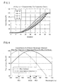
- Fig. 1 schematically shows a flow of the display driving carried out in the liquid crystal display device 10.
- Fig. 1 schematically shows a flow of the display driving carried out in a conventional liquid crystal display device 500 for comparison.
- a cell thickness is determined so that pixels of blue, which has the shortest wavelength among R, G, and B, have optimum transmittance.
- a cell thickness is determined so that pixels of green, which has a longer wavelength than blue, have optimum transmittance.
- the following describes how a cell thickness is determined in designing a liquid crystal display panel.
- a liquid crystal display panel is designed so that as high transmittance as possible can be obtained.
- transmittance is determined by the retardation value u of light.
- the retardation value u is determined by birefringence of a liquid crystal material, a cell thickness, and a transmitting wavelength. Accordingly, in a case where the liquid crystal material has been already determined, a specific transmitting wavelength is used as a standard, and a cell thickness is selected so that a desired retardation value is obtained at the transmitting wavelength used as a standard.
- transmittance obtained from the equation (1) is transmittance of a liquid crystal layer.
- light emitted from a backlight transmits not only a liquid crystal layer, but also other components such as polarization plates.
- transmittance of a liquid crystal display device is calculated based on not only the transmittance obtained from the equation (i), but also transmittance of polarization plates, transmittance of a color filter, an aperture ratio of a liquid crystal panel, light focusing power of a backlight, etc.
- a cell thickness is determined on the basis of a retardation value which is based on a wavelength of blue light which has the shortest wavelength among R, G, and B as described above. This is because in a case where a cell thickness is determined on the basis of a retardation value which is based on a wavelength longer than the wavelength of blue, there arises a problem that, in a high gradation region, grayscale inversion occurs in pixels having a color whose wavelength is shorter than the wavelength based on which the retardation value is determined.
- the grayscale inversion is a phenomenon by which transmittance of an image obtained by a low gradation value is made higher than transmittance of an image obtained by a high gradation value. This can cause a reduction in display quality.
- Fig. 3 shows an example in which grayscale inversion occurs.
- Fig. 3 shows gradation-transmittance characteristics (y characteristics) for respective colors that are obtained in a case where a cell thickness is set to 3.8 ⁇ m and where gradation characteristics are determined on the basis of white (mixture of R, G, and B) light.
- grayscale inversion occurs for blue which has the shortest wavelength.
- a cell thickness is determined on the basis of a retardation value which is based on the wavelength of blue light which has the shortest wavelength among R, G, and B.
- a cell thickness is determined on the basis of a wavelength of a color whose wavelength is longer than blue so that transmittance is improved in green and red pixels.
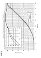
- Fig. 4 shows how transmittance changes depending on a wavelength in the liquid crystal display device 10 in which a cell thickness is determined on the basis of the wavelength of green (see the solid line).
- Fig. 4 also shows how transmittance changes depending on a wavelength in the liquid crystal display device 500 in which a cell thickness is determined on the basis of the wavelength of blue (see the broken line).
- transmittance reaches a maximum in the vicinity of blue (in the vicinity of 450 nm), and transmittance becomes smaller as the wavelength becomes larger from the vicinity of green (vicinity of 550 nm) to the vicinity of red (vicinity of 620 nm).
- transmittance reaches a maximum in the vicinity of green (in the vicinity of 550 nm), and transmittance becomes smaller as the distance from this wavelength becomes larger.
- a degree of reduction in transmittance in the vicinity of red (in the vicinity of 620 nm) is smaller as compared to the conventional liquid crystal display device 500. Accordingly, the liquid crystal display device 10 can achieve brighter display on the whole as compared to the conventional liquid crystal display device 500.
- a cell thickness d is, for example, 3.8 ⁇ min a case where birefringence ⁇ n of a liquid crystal material is 0.130, for example.
- the R, G, and B video signals are subjected to different gradation value conversion (y conversion) in the display control circuit 15 (see Fig. 1 ). This is described below with reference to Figs. 2 and 5 .
- the display data switching circuit 23 carries out gradation value shifting processing for shifting input gradation values to lower gradation values. This gradation conversion is carried out with reference to the look-up table 26.
- gradation conversion processing similar to a conventional one is carried out. Also in this case, the gradation conversion is carried out with reference to the look-up tables 24 and 25 that correspond to the display data switching circuits 21 and 22, respectively.
- Fig. 5 shows a relationship between a gradation value of the blue image data and transmittance in the liquid crystal display device 10 which relationship is obtained after the gradation value shifting processing is carried out.
- a gradation-transmittance characteristic of the blue image data of the present embodiment is indicated by the solid line (without white circles), and a gradation-transmittance characteristic of blue image data that has not been subjected to the gradation shifting processing is indicated as a comparative example by the line with white circles.
- An upper left corner of the graph of Fig. 5 shows an enlarged view of a high gradation side (gradation values 54 through 63) in which grayscale inversion can occur.
- the gradation value 58 at which transmittance is highest is used as the gradation value 63. That is, in a case where an input gradation value is 63, the display data switching circuit 23 shifts the gradation value 63 to the lower gradation value 58. In this way, the display data switching circuit 23 shifts input gradation values to lower gradation values so that output gradation values become smaller than the input gradation values in every gradation region.
- the pseudo multi-gradation circuit 27 carries out interpolation of gradation values in order to prevent a tone jump caused by a reduction in the number of available gradations that occurs as a result of the gradation value shifting processing.
- the pseudo multi-gradation circuit 27 carries out pseudo multi-gradation processing with respect to image data by using a known multi-gradation technique.
- the pseudo multi-gradation processing is processing which causes a human eye to believe that the number of gradations that can be expressed has increased although the number of gradations that can be expressed is limited in fact. This utilizes nature of the human eye (i.e., the human eye perceives, as luminance, time- and space-averaged luminance).
- the pseudo multi-gradation processing is classified into various types (e.g. FRC) depending on a size of a pixel region which serves as a unit or design of a noise pattern (i.e., noise pattern in each frame, the number of periodic frames etc.).
- Patent Literature 2 Japanese Patent Application Publication, Tokukai, No. 2005-10520A (Publication Date: January 13, 2005 ) discloses a specific method of the pseudo multi-gradation processing. This method is applicable also to the present invention.
- the pseudo multi-gradation processing makes it possible to achieve gradation expressing capability equivalent to that of general image display using gradation values 0 to 63 even though the number of available gradations is reduced by the gradation value shifting processing.
- Fig. 5 shows an example in which 6-bit (gradation values 0 to 63) gradation data is used, but the present invention is not limited to this.
- Fig. 6 is a graph showing a relationship between a wavelength of light and a luminosity factor in the liquid crystal display device 10 of the present embodiment.
- a luminosity factor in the liquid crystal display panel of the present embodiment is indicated by the solid line, and a luminosity factor obtained in a case where a cell thickness is determined on the basis of blue is indicated by the broken line for comparison.
- the luminosity factor is improved on the whole especially around the wavelength of green light (in the vicinity of 550 nm), as compared to the conventional example indicated by the broken line.
- Human eyes have high sensitivity to green light, and therefore tend to feel higher brightness as transmittance of green pixels becomes higher.
- Fig. 7 shows a result of evaluation of panel properties in the liquid crystal display device 10.
- a liquid crystal display panel in which a cell thickness is determined based on blue light is shown as a conventional art
- a liquid crystal display panel in which a cell thickness is determined based on green light but in which the gradation value shifting processing is not carried out is shown as a comparative example.
- a cell thickness is 3.1 ⁇ m which is determined based on the blue light.
- a cell thickness is determined based on green light, and is therefore larger than the panel of the conventional art.
- the cell thickness of each of the panels of the comparative example and the present Embodiment 1 is 3.8 ⁇ m.
- Fig. 7 also shows transmittance ratios in the blue, green, and red display (indicated by "Blue”, “Green”, and “Red” in Fig. 7 ).
- the bottom of the table of Fig. 7 shows presence or absence of grayscale inversion (presence of grayscale inversion is indicated by “x (OCCUR)", and absence of grayscale inversion is indicated by “o (NOT OCCUR)”).
- x OCCUR
- o NOT OCCUR
- Fig. 7 in the panel of the comparative example, grayscale inversion occurs in a blue image, whereas no grayscale inversion occurs in the panel of Embodiment 1 in which the gradation value shifting processing is carried out with respect to the blue image data. It can be hypothesized that this is reflected in the transmittance ratio of blue display, transmittance ratio of white display, and actual measurement values of transmittance.
- Fig. 23 shows simulation values of luminance ratios among R, G, and B of a color filter and transmittance ratios of the liquid crystal display device that are obtained in a case where a cell thickness is determined based on B, G, and R, respectively.
- the upper table of Fig. 23 shows values obtained in a case where no digital ⁇ processing is carried out (i.e., case where only the process of changing a cell thickness is carried out)
- the lower table of Fig. 23 shows values obtained in a case where the digital y processing is carried out.
- the "G optimum" row of the lower table of Fig. 23 shows simulation values for the liquid crystal display device of the present embodiment. Note that, in an actual liquid crystal display device, light focusing power of a backlight and polarization plates affect these simulation values.
- a cell thickness is determined on the basis of a retardation value which is based not on the wavelength of blue light which has the shortest wavelength among R, G, and B, but on the wavelength of green light. This allows not only an improvement in transmittance of green pixels, but also an improvement in transmittance of red pixels, thereby improving overall transmittance of an image displayed by a combination of R, G, and B.
- a cell thickness is determined so that transmittance in green pixels having a high luminosity factor becomes optimum, it is possible to display an image which allows a person to feel higher brightness.
- the present embodiment has dealt with an example in which a TN mode liquid crystal display panel is used.
- the present invention is not limited to this, and can be also applied to liquid crystal display panels of other modes such as IPS mode and VA mode.
- the present embodiment has dealt with an example in which a normally white mode liquid crystal display panel is used.
- the present invention is not limited to this, and can be also applied to a normally black mode liquid crystal display panel.
- Embodiment 2 of the present invention is described below with reference to Figs. 8 through 14 .
- the present embodiment mainly discusses differences from Embodiment 1, and in a case where configuration and driving method similar to those of Embodiment 1 can be applied, explanation of such configuration and driving method are omitted.
- the present embodiment also deals with, as an example, a liquid crystal display device which includes a TN mode liquid crystal display panel and in which polarization plates are disposed so that normally white mode can be realized, as in Embodiment 1.
- Fig. 8 illustrates a configuration of a liquid crystal display device 110 of the present embodiment.
- the liquid crystal display device 110 mainly includes: a liquid crystal display panel (LCD panel) 11, a gate driving circuit 12, a source driving circuit 13, a timing controller 14, and a display control circuit 115 (gradation conversion section).
- LCD panel liquid crystal display panel
- gate driving circuit 12 a gate driving circuit 12
- source driving circuit 13 a source driving circuit 13
- timing controller 14 a display control circuit 115 (gradation conversion section).
- the liquid crystal display panel (LCD panel) 11, gate driving circuit 12, source driving circuit 13, and timing controller 14 have similar arrangements to those of the liquid crystal display device 10 of Embodiment 1, and therefore are not explained repeatedly.
- the display control circuit 115 carries out data processing with respect to inputted video signals of respective colors (R, G, and B) and supplies gradation data to R, G, and B pixels within the liquid crystal display panel 11.
- the gradation data that has been subjected to the data processing in the display control circuit 115 is supplied to the pixels within the liquid crystal display panel 11 via the timing controller 14 and the source driving circuit 13. Thus, an image based on the inputted video signals is displayed.
- the display control circuit 115 includes display data switching circuits 121, 122, and 123 (gradation conversion sections) and look-up tables (LUTs) 124, 125, and 126.
- the display data switching circuits 121, 122, and 123 are circuits which generate, from inputted video signals, image data for performing desired image display.
- gradation conversion processing y conversion processing
- the look-up tables are tables in which input gradation values are associated one-to-one with output gradation values.
- the display data switching circuits and LUTs are associated with different video signals. Specifically, the display data switching circuit 121 and the LUT 124 are associated with a red video signal, the display data switching circuit 122 and the LUT 125 are associated with a green video signal, and the display data switching circuit 123 and the LUT 126 are associated with a blue video signal. This makes it possible to carry out different gradation conversion processing with respect to video signals of different colors.
- the display control circuit 115 includes pseudo multi-gradation circuits 127 and 128 (pseudo multi-gradation sections) for carrying out pseudo multi-gradation processing with respect to image data.
- the pseudo multi-gradation circuits 127 and 128 are provided in the series of processing circuits for the blue image data and in the series of processing circuits for the green image data, respectively, since pseudo multi-gradation processing is carried out only with respect to image data subjected to gradation value shifting processing.
- the following description deals with display driving carried out in the liquid crystal display device 110.
- a cell thickness is determined so that pixels of blue which has the shortest wavelength among R, G, and B have optimum transmittance (see (b) of Fig. 1 ).
- a cell thickness is determined on the basis of a wavelength of a color whose wavelength is longer than that of blue so that transmittance in green and red pixels is improved, as in Embodiment 1.
- a cell thickness is determined so that pixels of red which has a longer wavelength than blue and green have optimum transmittance.
- the cell thickness determining method described in Embodiment 1 can be applied also to the present embodiment. However, since, in the present embodiment, a cell thickness is determined so that red pixels have optimum transmittance, the transmitting wavelength ⁇ used as a standard in the equation 2 is set to 620 nm which is the wavelength of red, and a cell thickness is selected so that a desired retardation value can be obtained at this transmitting wavelength.
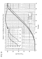
- Fig. 10 shows how transmittance changes depending on a wavelength in the liquid crystal display device 110 in which a cell thickness is determined on the basis of the wavelength of red (see the solid line).
- Fig. 10 also shows how transmittance changes depending on a wavelength in the conventional liquid crystal display device 500 in which a cell thickness is determined on the basis of the wavelength of blue (see the broken line).
- transmittance reaches a maximum in the vicinity of blue (in the vicinity of 450 nm), and transmittance becomes smaller as the wavelength becomes larger from the vicinity of green (vicinity of 550 nm) to the vicinity of red (vicinity of 620 nm).
- transmittance reaches a maximum in the vicinity of red (in the vicinity of 620 nm), and transmittance becomes smaller as the distance from this wavelength becomes larger.
- transmittance at the wavelength in the vicinity of green (in the vicinity of 550 nm), which has the highest luminosity factor among R, G, and B, is higher than that of the conventional liquid crystal display device 500. Accordingly, the liquid crystal display device 110 can achieve brighter display on the whole as compared to the conventional liquid crystal display device 500.
- a cell thickness d is, for example, 4.2 ⁇ m in a case where birefringence ⁇ n of a liquid crystal material is 0.130, for example.
- Fig. 9 shows gradation-transmittance characteristics (y characteristics) for respective colors that are obtained in a case where a cell thickness is set to 4.2 ⁇ m on the basis of red and where gradation characteristics are determined on the basis of white (mixture of R, G, and B) light.
- y characteristics gradation-transmittance characteristics
- the display control circuit 115 carries out different gradation value conversion (y conversion) with respect to R, G, and B video signals (see (a) of Fig. 1 ). This is described below with reference to Figs. 8 , 11 , and 12 .
- gradation value shifting processing for shifting input gradation values to lower gradation values is carried out in the display data switching circuits 122 and 123. This gradation conversion is carried out with reference to the look-up tables 125 and 126.
- gradation conversion processing similar to the conventional one is carried out. Also in this case, the gradation conversion is carried out with reference to the look-up table 124 that corresponds to the display data switching circuit 121.
- Fig. 11 shows a relationship between a gradation value of the blue image data and transmittance in the liquid crystal display device 110 which relationship is obtained after the gradation value shifting processing is carried out.
- a gradation-transmittance characteristic of the blue image data of the present embodiment is indicated by the solid line (without white circles), and a gradation-transmittance characteristic of blue image data that has not been subjected to the gradation shifting processing is indicated as a comparative example by the line with white circles.
- An upper left portion of the graph of Fig. 11 shows an enlarged view of a higher gradation side (gradation values 54 through 63) in which grayscale inversion can occur.
- the gradation value 57 at which transmittance is highest is used as the gradation value 63. That is, in a case where an input gradation value is 63, the display data switching circuit 123 shifts the gradation value to a lower gradation value 57. In this way, the display data switching circuit 123 shifts input gradation values to lower gradation values so that output gradation values become smaller than the input gradation values in every gradation region.
- Fig. 12 shows a relationship between a gradation value of the green image data and transmittance in the liquid crystal display device 110 which relationship is obtained after the gradation value shifting processing is carried out.
- a gradation-transmittance characteristic of the green image data of the present embodiment is indicated by the solid line (without white circles), and a gradation-transmittance characteristic of green image data that has not been subjected to the gradation shifting processing is indicated as a comparative example by the line with white circles.
- An upper left portion of the graph of Fig. 12 shows an enlarged view of a higher gradation side (gradation values 54 through 63) in which grayscale inversion can occur.
- the display data switching circuit 122 shifts the gradation value to a lower gradation value 60. In this way, the display data switching circuit 122 shifts input gradation values to lower gradation values so that output gradation values become smaller than the input gradation values in every gradation region.
- the pseudo multi-gradation circuits 127 and 128 carry out interpolation of gradation values in order to prevent a tone jump caused by reduction in the number of available gradations that occurs due to the gradation value shifting process.
- the pseudo multi-gradation processing carried out in the pseudo multi-gradation circuits 127 and 128 is similar to that described in Embodiment 1, and therefore is not explained repeatedly.
- the pseudo multi-gradation processing makes it possible to achieve gradation expressing capability equivalent to that of general image display using gradation values 0 to 63 even though the number of available gradations is reduced by the gradation value shifting processing.
- Figs. 11 and 12 show an example in which 6-bit (gradation values 0 to 63) gradation data is used, but the present invention is not limited to this.
- Fig. 13 is a graph showing a relationship between a wavelength of light and a luminosity factor in the liquid crystal display device 110 of the present embodiment.
- a luminosity factor in the liquid crystal display panel of the present embodiment is indicated by the solid line, and a luminosity factor obtained in a case where a cell thickness is determined on the basis of blue is indicated by the broken line for comparison.
- the luminosity factor is improved on the whole especially around the wavelength of red light (in the vicinity of 620 nm), as compared to the conventional example indicated by the broken line.
- Fig. 14 shows a result of evaluation of panel properties in the liquid crystal display device 110.
- a liquid crystal display panel in which a cell thickness is determined based on blue light is shown as a conventional art, and a liquid crystal display panel in which a cell thickness is determined based on red light but in which the gradation value shifting processing is not carried out is shown as a comparative example.
- a cell thickness is 3.1 ⁇ m which is determined based on the blue light.
- a cell thickness is determined based on red light, and is therefore larger than that of the conventional art.
- the cell thickness of each of the panels of the comparative example and the present Embodiment 2 is 4.2 ⁇ m
- Fig. 14 also shows transmittance ratios in the blue, green, and red display (indicated by "Blue”, “Green”, and “Red” in Fig. 14 ).
- the bottom of the table of Fig. 14 shows presence or absence of grayscale inversion (presence of grayscale inversion is indicated by “x (OCCUR)", and absence of grayscale inversion is indicated by “o (NOT OCCUR)”).
- x OCCUR
- o NOT OCCUR
- Fig. 14 in the panel of the comparative example, grayscale inversion occurs in blue and green images, whereas no grayscale inversion occurs in the panel of Embodiment 2 in which the gradation value shifting processing is carried out with respect to the blue and green image data. It can be hypothesized that this is reflected in the transmittance ratios of blue display and green display, transmittance ratio of white display, and actual measurement values of transmittance.
- Fig. 23 shows simulation values of luminance ratios among R, G, and B of a color filter and transmittance ratios of the liquid crystal display device that are obtained in a case where a cell thickness is determined based on B, G, and R, respectively.
- the upper table of Fig. 23 shows values obtained in a case where no digital y processing is carried out (i.e., case where only the process of changing a cell thickness is carried out)
- the lower table of Fig. 23 shows values obtained in a case where the digital y processing is carried out.
- the "R optimum" row of the lower table of Fig. 23 shows simulation values for the liquid crystal display device of the present embodiment. Note that, in an actual liquid crystal display device, light focusing power of a backlight and polarization plates affect these simulation values.
- a cell thickness is determined on the basis of a retardation value which is based not on the wavelength of blue light which has the shortest wavelength among R, G, and B, but on the wavelength of red light. This allows not only an improvement in transmittance of red pixels, but also an improvement in transmittance of green pixels, thereby improving overall transmittance of an image displayed by a combination of R, G, and B.
- the cell thickness can be made larger as compared with a case where the cell thickness is determined on the basis of blue or green. This produces an effect of improvement in durability of a liquid crystal display panel against mixing in of a foreign substance such as dust.
- Embodiment 3 of the present invention is described below with reference to Figs. 15 through 22 .
- the present embodiment mainly discusses differences from Embodiment 1, and in a case where configuration and driving method similar to those of Embodiment 1 can be applied, explanation of such configuration and driving method are omitted.
- the present embodiment also deals with, as an example, a liquid crystal display device which includes a TN mode liquid crystal display panel and in which polarization plates are disposed so that normally white mode can be realized, as in Embodiment 1.
- Fig. 15 illustrates a configuration of a liquid crystal display device 210 of the present embodiment.
- the liquid crystal display device 210 mainly includes: a liquid crystal display panel (LCD panel) 11, a gate driving circuit 12, a source driving circuit 13, a timing controller 14, and a display control circuit 215 (gradation conversion section).
- LCD panel liquid crystal display panel
- gate driving circuit 12 a gate driving circuit 12
- source driving circuit 13 a source driving circuit 13
- timing controller 14 a display control circuit 215 (gradation conversion section).
- the liquid crystal display panel (LCD panel) 11, gate driving circuit 12, source driving circuit 13, and timing controller 14 have similar arrangements to those of the liquid crystal display device 10 of Embodiment 1, and therefore are not explained repeatedly.
- the display control circuit 215 carries out data processing with respect to inputted video signals of respective colors (R, G, and B) and supplies gradation data to R, G, and B pixels within the liquid crystal display panel 11.
- the gradation data that has been subjected to the data processing in the display control circuit 215 is supplied to the pixels within the liquid crystal display panel 11 via the timing controller 14 and the source driving circuit 13. Thus, an image based on the inputted video signals is displayed.
- the display control circuit 215 includes display data switching circuits 221, 222, and 223 (gradation conversion sections) and look-up tables (LUTs) 224, 225, and 226.
- the display data switching circuits 221, 222, and 223 are circuits which generate, from inputted video signals, image data for performing desired image display.
- gradation conversion processing y conversion processing
- the look-up tables are tables in which input gradation values are associated one-to-one with output gradation values.
- the display data switching circuits and LUTs are associated with different video signals. Specifically, the display data switching circuit 221 and the LUT 224 are associated with a red video signal, the display data switching circuit 222 and the LUT 225 are associated with a green video signal, and the display data switching circuit 223 and the LUT 226 are associated with a blue video signal. This makes it possible to carry out different gradation conversion processing with respect to video signals of different colors.
- the display control circuit 215 includes pseudo multi-gradation circuits 227, 228, and 229 (pseudo multi-gradation sections) for carrying out pseudo multi-gradation processing with respect to image data.
- the pseudo multi-gradation processing is carried out with respect to image data subjected to gradation value shifting processing. Since, in the present embodiment, the gradation value shifting processing is carried out with respect to all of the R, G, and B image data, the pseudo multi-gradation circuits 227, 228, and 229 are provided in the series of processing circuits for blue image data, the series of processing circuits for green image data, and the series of processing circuits for red image data, respectively.
- the following description deals with display driving carried out in the liquid crystal display device 210.
- a cell thickness is determined so that pixels of blue which has the shortest wavelength among R, G, and B have optimum transmittance (see (b) of Fig. 1 ).
- a cell thickness is determined on the basis of a wavelength of a color whose wavelength is longer than that of blue so that transmittance in green and red pixels is improved, as in Embodiment 1.
- a cell thickness is determined so that transmittance becomes optimum at a wavelength (wavelength 670 nm) longer than the wavelength of red light.
- the cell thickness determining method described in Embodiment 1 can be applied also to the present embodiment. However, since, in the present embodiment, a cell thickness is determined so that transmittance of light having the wavelength 670 nm becomes optimum, the transmitting wavelength ⁇ used as a standard in the equation 2 is set to 670 nm, and a cell thickness is selected so that a desired retardation value can be obtained at this transmitting wavelength.
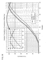
- Fig. 17 shows how transmittance changes depending on a wavelength in the liquid crystal display device 210 in which a cell thickness is determined on the basis of the wavelength 670 nm (see the solid line). Fig. 17 also shows how transmittance changes depending on a wavelength in the conventional liquid crystal display device 500 in which a cell thickness is determined on the basis of the wavelength of blue (see the broken line).
- transmittance reaches a maximum in the vicinity of blue (in the vicinity of 450 nm), and transmittance becomes smaller as the wavelength becomes larger from the vicinity of green (vicinity of 550 nm) to the vicinity of red (vicinity of 620 nm).
- transmittance reaches a maximum at the wavelength (in the vicinity of 670 nm) longer than the wavelength of red light, and transmittance becomes smaller as the distance from this wavelength becomes larger.
- a cell thickness d is, for example, 4.4 ⁇ m in a case where birefringence ⁇ n of a liquid crystal material is 0.130, for example.
- Fig. 16 shows gradation-transmittance characteristics (y characteristics) for respective colors that are obtained in a case where a cell thickness is set to 4.4 ⁇ m on the basis of the wavelength (specifically the wavelength 670 nm) longer than the wavelength of red and where gradation characteristics are determined on the basis of white (mixture of R, G, and B) light.
- y characteristics gradation-transmittance characteristics
- the display control circuit 215 carries out different gradation value conversion ( ⁇ conversion) with respect to R, G, and B video signals (see (a) of Fig. 1 ). This is described below with reference to Figs. 15 , 18 , 19 , and 20 .
- gradation value shifting processing for shifting input gradation values to lower gradation values is carried out in the display data switching circuits 221, 222, and 123. This gradation conversion is carried out with reference to the look-up tables 224, 225, and 226.
- Fig. 18 shows a relationship between a gradation value of the blue image data and transmittance in the liquid crystal display device 210 which relationship is obtained after the gradation value shifting processing is carried out.
- a gradation-transmittance characteristic of the blue image data of the present embodiment is indicated by the solid line (without white circles), and a gradation-transmittance characteristic of blue image data that has not been subjected to the gradation shifting processing is indicated as a comparative example by the line with white circles.
- An upper left portion of the graph of Fig. 18 shows an enlarged view of a higher gradation side (gradation values 54 through 63) in which grayscale inversion can occur.
- the gradation value 58 at which transmittance is highest is used as the gradation value 63. That is, in a case where an input gradation value is 63, the display data switching circuit 223 shifts the gradation value to a lower gradation value 58. In this way, the display data switching circuit 223 shifts input gradation values to lower gradation values so that output gradation values become smaller than the input gradation values in every gradation region.
- Fig. 19 shows a relationship between a gradation value of the green image data and transmittance in the liquid crystal display device 210 which relationship is obtained after the gradation value shifting processing is carried out.
- a gradation-transmittance characteristic of the green image data of the present embodiment is indicated by the solid line (without white circles), and a gradation-transmittance characteristic of green image data that has not been subjected to the gradation shifting processing is indicated as a comparative example by the line with white circles.
- An upper left portion of the graph of Fig. 19 shows an enlarged view of a higher gradation side (gradation values 54 through 63) in which grayscale inversion can occur.
- the display data switching circuit 222 shifts the gradation value to a lower gradation value 60. In this way, the display data switching circuit 222 shifts input gradation values to lower gradation values so that output gradation values become smaller than the input gradation values in every gradation region.
- Fig. 20 shows a relationship between a gradation value of the red image data and transmittance in the liquid crystal display device 210 which relationship is obtained after the gradation value shifting processing is carried out.
- a gradation-transmittance characteristic of the red image data of the present embodiment is indicated by the solid line (without white circles), and a gradation-transmittance characteristic of red image data that has not been subjected to the gradation shifting processing is indicated as a comparative example by the line with white circles.
- An upper left portion of the graph of Fig. 20 shows an enlarged view of a higher gradation side (gradation values 57 through 63) in which grayscale inversion can occur.
- grayscale inversion occurs at the highest gradation value 63.
- the gradation value 62 at which transmittance is highest is used as the gradation value 63. That is, in a case where an input gradation value is 63, the display data switching circuit 221 shifts the gradation value to a lower gradation value 62. In this way, the display data switching circuit 221 shifts input gradation values to lower gradation values so that output gradation values become smaller than the input gradation values in every gradation region.
- the pseudo multi-gradation circuits 227, 228, and 229 carry out interpolation of gradation values in order to prevent a tone jump caused by reduction in the number of available gradations that occurs due to the gradation value shifting process.
- the pseudo multi-gradation processing carried out in the pseudo multi-gradation circuits 227, 228, and 229 is similar to that described in Embodiment 1, and therefore is not explained repeatedly.
- the pseudo multi-gradation processing makes it possible to achieve gradation expressing capability equivalent to that of general image display using gradation values 0 to 63 even though the number of available gradations is reduced by the gradation value shifting processing.
- Figs. 18 , 19 , and 20 show an example in which 6-bit (gradation values 0 to 63) gradation data is used, but the present invention is not limited to this.
- Fig. 21 is a graph showing a relationship between a wavelength of light and a luminosity factor in the liquid crystal display device 210 of the present embodiment.
- a luminosity factor in the liquid crystal display panel of the present embodiment is indicated by the solid line, and a luminosity factor obtained in a case where a cell thickness is determined on the basis of blue is indicated by the broken line for comparison.
- the luminosity factor is improved on the whole, as compared to the conventional example indicated by the broken line. This is because transmittance of green and red light can be improved as shown in Fig. 23 since a cell thickness is determined on the basis of the wavelength 670 nm.
- Fig. 22 shows a result of evaluation of panel properties in the liquid crystal display device 210.
- a liquid crystal display panel in which a cell thickness is determined based on blue light is shown as a conventional art
- a liquid crystal display panel in which a cell thickness is determined based on the wavelength (specifically the wavelength 670 nm) longer than the wavelength of red but in which the gradation value shifting processing is not carried out is shown as a comparative example.
- a cell thickness is 3.1 ⁇ m which is determined based on the blue light.
- a cell thickness is determined based on light of 670 nm, and is therefore larger than that of the conventional art.
- the cell thickness of each of the panels of the comparative example and the present Embodiment 3 is 4.4 ⁇ m
- Fig. 22 also shows transmittance ratios in the blue, green, and red display (indicated by "Blue”, “Green”, and “Red” in Fig. 22 ).
- the bottom of the table of Fig. 22 shows presence or absence of grayscale inversion (presence of grayscale inversion is indicated by “x (OCCUR)", and absence of grayscale inversion is indicated by “o (NOT OCCUR)”).
- x OCCUR
- o NOT OCCUR
- Fig. 22 in the panel of the comparative example, grayscale inversion occurs in blue, green, and red images, whereas no grayscale inversion occurs in the panel of Embodiment 3 in which the gradation value shifting processing is carried out. It can be hypothesized that this is reflected in the transmittance ratios of blue, green, and red display, transmittance ratio of white display, and actual measurement values of transmittance.
- Fig. 23 shows simulation values of luminance ratios among R, G, and B of a color filter and transmittance ratios of the liquid crystal display device that are obtained in a case where a cell thickness is determined based on B, G, and R, respectively.
- the upper table of Fig. 23 shows values obtained in a case where no digital y processing is carried out (i.e., case where only the process of changing a cell thickness is carried out)
- the lower table of Fig. 23 shows values obtained in a case where the digital ⁇ processing is carried out.
- a cell thickness is determined on the basis of a retardation value which is based not on blue light which has the shortest wavelength among R, G, and B, but on light having the wavelength longer than the wavelength of red light. This allows not only an improvement in transmittance of pixels of red which has a wavelength close to this wavelength, but also an improvement in overall transmittance of an image displayed by a combination of R, G, and B.
- the cell thickness can be made larger as compared with a case where the cell thickness is determined on the basis of blue or green. This produces an effect of improvement in durability of a liquid crystal display panel against mixing in of a foreign substance such as dust.
- liquid crystal display device of the present invention allows an improvement in transmittance of a displayed image.
- the liquid crystal display device of the present invention is applicable to a color liquid crystal display device.
Landscapes
- Engineering & Computer Science (AREA)
- Chemical & Material Sciences (AREA)
- Crystallography & Structural Chemistry (AREA)
- Physics & Mathematics (AREA)
- Computer Hardware Design (AREA)
- General Physics & Mathematics (AREA)
- Theoretical Computer Science (AREA)
- Control Of Indicators Other Than Cathode Ray Tubes (AREA)
- Liquid Crystal Display Device Control (AREA)
- Liquid Crystal (AREA)
Abstract
Description
- The present invention relates to a liquid crystal display device which displays a color image with the use of color filters of plural colors and a method for driving the liquid crystal display device.
- Liquid crystal display devices are flat display devices which have excellent features such as high definition, low profile, light weight, and low power consumption. In recent years, a market scale of liquid crystal display devices has been rapidly increasing due to improved display performance, increased production capacity, and improved price competitiveness against other display devices.
- In a twisted nematic mode (TN mode) liquid crystal display device which is widely used today, long axes of liquid crystal molecules having positive dielectric anisotropy are aligned substantially parallel to a substrate surface, and the long axes of the liquid crystal molecules are twisted by substantially 90° between upper and lower substrates along a thickness direction of a liquid crystal layer. When a voltage is applied to the liquid crystal layer, the liquid crystal molecules are aligned parallel to an electric field, and twist alignment is eliminated. In a TN mode liquid crystal display device, light transmittance is controlled by utilizing a change in optical rotation caused by a change in alignment of liquid crystal molecules which occurs due to voltage application.
- In designing a panel of such a liquid crystal display device, it is necessary that retardation of light be a desired value in order to realize as high transmittance as possible.
- Here, a retardation value u is determined by the following equation:

where Δn is refractive index anisotropy (birefringence) of a liquid crystal material, d is a cell thickness, and λis a wavelength of light. According to the equation, the thickness (also referred to as cell thickness) of a liquid crystal layer of a liquid crystal display panel is determined based on the refractive index anisotropy Δn which is determined based on the type of the liquid crystal material, the wavelength λof light used as a standard, and the retardation value u for obtaining the desired transmittance. - Generally, in a TN mode liquid crystal display device which displays a color image of mixed colors of R, G, and B, a cell thickness of a liquid crystal panel is determined on the basis of retardation which is based on the wavelength of blue light, which has the shortest wavelength among the three colors (red (R), green (G), and blue (B)) of color filters (see
Patent Literature 1, for example). -
- Japanese Patent Application Publication, Tokukaisho, No.
61-98330 A (Publication Date: May 16, 1986 - However, in a case where a cell thickness is determined on the basis of the wavelength of blue light which is the shortest wavelength as above, there occurs a problem that sufficient transmittance cannot be obtained in pixels of green and red which have longer wavelength than blue light.
-
Fig. 24 shows how transmittance of a liquid crystal display panel changes depending on a wavelength in a case where a cell thickness is determined in accordance with a current method for determining the cell thickness of a liquid crystal display panel such that a retardation value becomes optimum at the wavelength of blue which is the shortest wavelength. As shown inFig. 24 , transmittance of blue pixels has an optimum value (1 in this case) since a cell thickness of a current liquid crystal display panel is designed so that retardation becomes optimum at the wavelength of blue. Meanwhile, transmittance of green and red pixels is lower than the optimum value. - For example,
Patent Literature 1 discloses that in a case where refractive index anisotropy Δn of a liquid crystal material is 0.18 and where a thickness (cell thickness) of a liquid crystal layer is 7mm, a blue pixel has transmittance of 100%, whereas a green pixel and a red pixel have reduced transmittance of 98% and 88%, respectively. - In the multi-color liquid crystal display device disclosed in
Patent Literature 1, transmittance of pixels having colors other than blue is improved by causing a liquid crystal layer to have different thicknesses above blue, green, and red pixels. However, the technique disclosed inPatent Literature 1 of changing a cell thickness depending on a pixel color complicates a panel manufacturing process. Moreover, there is a problem that even a slight misalignment between an active matrix substrate and a counter substrate causes cell thicknesses for the respective colors to be different from optimum values. - The present invention was attained in view of the above problems, and an object of the present invention is to provide a color liquid crystal display device in which transmittance of pixels having colors whose wavelengths are not the shortest one is improved without changing a pixel structure depending on color.
- In order to attain the above object, a liquid crystal display device includes a liquid crystal display panel which has pixels of different colors and which displays a color image with use of the pixels, the liquid crystal display panel including two substrates and a liquid crystal layer sandwiched between the two substrates, and the liquid crystal layer having a thickness that is determined on a basis of a retardation value which is based on light which has a wavelength larger than light having shortest wavelength among light of the different colors.
- In general, a thickness (also referred to as cell thickness) is determined based on birefringence Δn which is determined based on the type of a liquid crystal material, a wavelength λof light used as a standard, and a retardation value u for obtaining desired transmittance. That is, the cell thickness is determined on the basis of light having a specific wavelength so that desired transmittance can be obtained in a liquid crystal display device. In a conventional color liquid crystal display device which displays a color image with use of pixels of difference colors, a cell thickness is determined on the basis of light of a color having the shortest wavelength among the different colors so that optimum transmittance can be obtained in pixels of the color having the shortest wavelength. For example, in a case where the liquid crystal display device has pixels of red, green, and blue, the cell thickness is determined on the basis of a retardation value which is based on a wavelength of blue light so that optimum transmittance can be obtained in blue pixels. However, according to this cell thickness determining method, sufficient transmittance cannot be obtained in pixels (e.g., red pixels and green pixels) of colors having wavelengths other than the shortest wavelength.
- In view of this, in the present invention, a cell thickness is determined on the basis of a retardation value which is based on light having a larger wavelength than light having the shortest wavelength among light having colors of pixels.
- According to the arrangement, transmittance can be improved in pixels of colors having wavelengths other than the shortest wavelength.
- For example, in a liquid crystal display device which displays a multi-color image in a mixture color of red (R), green (G), and blue (B), a transmittance ratio among R, G, and B of a color filter (specifically, a luminance ratio among R, G, and B of the color filter illuminated by a white light source) is (1.3 to 2.0) : (3.0 to 7.0) : 1 in a case where blue is used as a standard. That is, green and red, each of which has a longer wavelength than blue, make higher contribution to transmittance obtained in a case where R, G, and B are mixed, as compared to blue.
- Overall transmittance obtained by multiplying transmittance of R, G, and B can be made higher in a case where a cell thickness is determined on the basis of green or red each of which has a longer wavelength than blue, as compared with a case where a cell thickness is determined on the basis of blue having the shortest wavelength. A right end column of
Fig. 23 shows a ratio of (i) transmittance obtained in a case where a cell thickness is determined on the basis of B (B optimum), (ii) transmittance obtained in a case where a cell thickness is determined on the basis of G (G optimum), and (iii) transmittance obtained in a case where a cell thickness is determined on the basis of R (R optimum). InFig. 23 , the transmittance obtained in a case where the cell thickness is determined on the basis of B (B optimum) is set to 100%. Note that the upper table ofFig. 23 shows values obtained in a case where no digital y processing is carried out (i.e., case where only the process of changing a cell thickness is carried out), and the lower table ofFig. 23 shows values obtained in a case where the digital γ processing is carried out. - According to the arrangement, transmittance of a displayed image can be improved, but there occurs a problem that grayscale inversion occurs in image data supplied to pixels of a color having a shorter wavelength than a wavelength based on which the cell thickness is determined. The grayscale inversion is a phenomenon by which transmittance of an image obtained by a low gradation value is made higher than transmittance of an image obtained by a high gradation value.
- In view of this, the liquid crystal display device of the present invention is preferably arranged to further include a gradation conversion section that carries out gradation value shifting processing of shifting input gradation values to lower gradation values with respect to image data supplied to pixels having a color which has a shorter wavelength than the wavelength based on which the thickness of the liquid crystal layer is determined.
- According to the arrangement, the liquid crystal display device includes a gradation conversion section that carries out gradation value shifting processing of shifting input gradation values to lower gradation values with respect to image data supplied to pixels having a color which has a shorter wavelength than the wavelength based on which the thickness of the liquid crystal layer is determined. This makes it possible to prevent grayscale inversion in the pixels having the color which has the shorter wavelength, thereby allowing an improvement in quality of a displayed image.
- It is preferable that the gradation value shifting processing is processing for shifting the highest gradation value to a gradation value that is lower than the highest gradation value by 1 so that the gradation value at which grayscale inversion occurs is not used.
- The liquid crystal display device of the present invention is preferably arranged such that the gradation value shifting processing varies depending on the color of the pixels.
- In a case where the grayscale inversion occurs, the lowest gradation value in a high gradation region in which grayscale inversion occurs varies depending on a color of image data.
- According to the arrangement, in which the gradation value shifting processing varies depending on the color of the pixels, it is possible to carry out desirable gradation conversion processing with respect to each of the image data of different colors.
- Carrying out gradation value shifting processing which varies depending on the color of the pixels means that even if the image data of the different colors have the same target gradation (same input gradation), output gradation is caused to vary depending on the color so that a gradation voltage which varies depending on the color is supplied to a pixel electrode. Further, in a case where the gradation value shifting processing is carried out with reference to look-up tables, carrying out gradation value shifting processing which varies depending on the color of the pixels means that the gradation value shifting processing is carried out with reference to look-up tables which are different from one color to another.
- The liquid crystal display device of the present invention is preferably arranged to further include a pseudo multi-gradation section which carries out pseudo multi-gradation processing with respect to the image data that has been subjected to the gradation value shifting processing in the gradation conversion section.
- According to the arrangement, by carrying out the pseudo multi-gradation processing with respect to the image data that has been subjected to the gradation value shifting processing, it is possible to suppress a reduction in gradation expressing capability caused by a reduction in the number of available gradations.
- The liquid crystal display device of the present invention is preferably arranged such that the gradation conversion section has a look-up table in which input gradation values are associated with output gradation values.
- According to the arrangement, the gradation conversion processing can be carried out with reference to the look-up table. This makes it possible to more easily carry out the conversion processing and to simplify configurations of circuits etc. necessary for the data conversion processing.
- The liquid crystal display device of the present invention may be arranged such that the liquid crystal display panel is constituted by pixels of blue, green, and red, and the thickness of the liquid crystal layer is determined on a basis of a retardation value which is based on a wavelength of green light or red light.
- According to the arrangement, a cell thickness is determined on the basis of a retardation value which is based on the wavelength of green or red each of which has a longer wavelength than blue among the three colors of the pixels. Accordingly, the cell thickness can be determined so that transmittance becomes optimum for image data having the selected color.
- The liquid crystal display device may be arranged such that the liquid crystal display panel is constituted by pixels of blue, green, and red, and the thickness of the liquid crystal layer is determined on a basis of a retardation value which is based on a wavelength of green light.
- Human eyes have high sensitivity to green light, and therefore tend to feel higher brightness as transmittance of green pixels becomes higher.
- According to the arrangement, the thickness of the liquid crystal layer is determined so that transmittance becomes optimum in the green pixels. Accordingly, it is possible to display an image which allows human eyes to feel higher brightness.
- The liquid crystal display device of the present invention may be arranged such that the liquid crystal display panel is constituted by pixels of blue, green, and red, and the thickness of the liquid crystal layer is determined on a basis of a retardation value which is based on a wavelength of red light or a wavelength that is longer than the wavelength of the red light.
- According to the arrangement, the cell thickness can be made larger as compared with the case where the cell thickness is determined on the basis of blue or green light. The thinner the cell thickness becomes, the more remarkable deterioration in quality caused by mixing in of dust etc. becomes. In a case where the cell thickness is determined on a basis of a wavelength of red light or a wavelength that is longer than the wavelength of the red light, the cell thickness can be made as large as 4.0 µm to 4.5 µm, which is larger as compared with the case where the cell thickness is determined on the basis of blue light. Accordingly, it is possible to suppress deterioration in panel quality caused by mixing in of dust etc.
- In order to attain the above object, a method for driving a liquid crystal display device including a liquid crystal display panel which has pixels of different colors and which displays a color image with use of the pixels, the liquid crystal display panel including two substrates and a liquid crystal layer sandwiched between the two substrates, includes the steps of: (a) determining a thickness of the liquid crystal layer on a basis of a retardation value which is based on light which has a wavelength larger than light having shortest wavelength among light of the different colors; and (b) carrying out gradation value shifting processing of shifting input gradation values to lower gradation values with respect to image data supplied to pixels having a color which has a shorter wavelength than the wavelength based on which the thickness of the liquid crystal layer is determined.
- According to the method, the cell thickness is determined on a basis of a retardation value which is based on a wavelength of light which has a larger wavelength than light having shortest wavelength among light of the different colors. Accordingly, transmittance can be improved in pixels of colors having wavelengths other than the shortest wavelength.
- According to the method, gradation value shifting processing of shifting input gradation values to lower gradation values is carried out with respect to image data supplied to pixels having a color which has a shorter wavelength than the wavelength based on which the cell thickness is determined. This makes it possible to prevent grayscale inversion in the pixels having the color which has the shorter wavelength, thereby allowing an improvement in quality of a displayed image.
- In the method of the present invention, it is preferable that the gradation value shifting processing carried out in the step (b) varies depending on the color of the pixels.
- In a case where the grayscale inversion occurs, the lowest gradation value in a high gradation region in which grayscale inversion occurs varies depending on a color of image data.
- According to the method, in which the gradation value shifting processing varies depending on the color of the pixels, it is possible to carry out desirable gradation conversion processing with respect to each of the image data of different colors.
- The method of the present invention preferably includes the step of (c) carrying out pseudo multi-gradation processing with respect to the image data that has been subjected to the gradation value shifting processing.
- According to the method, by carrying out the pseudo multi-gradation processing with respect to the image data that has been subjected to the gradation value shifting processing, it is possible to suppress a reduction in gradation expressing capability caused by a reduction in the number of available gradations.
- In the method of the present invention, it is preferable that in the step (b), the gradation value shifting processing is carried out with reference to a look-up table in which the input gradation values are associated with output gradation values.
- According to the method, the gradation conversion processing can be carried out with reference to the look-up table. This makes it possible to more easily carry out the conversion processing and to simplify configurations of circuits etc. necessary for the data conversion processing.
- According to the liquid crystal display device of the present invention, the liquid crystal display device includes two substrates and a liquid crystal layer sandwiched between the two substrates, and the thickness of the liquid crystal layer is determined on the basis of a retardation value which is based on light having a wavelength larger than light having the shortest wavelength among light of the different colors.
- According to the arrangement, transmittance can be improved in pixels of colors having wavelengths other than the shortest wavelength.
- The method for driving a liquid crystal display device includes the steps of: (a) determining a thickness of the liquid crystal layer on a basis of a retardation value which is based on light which has a wavelength larger than light having shortest wavelength among light of the different colors; and (b) carrying out gradation value shifting processing of shifting input gradation values to lower gradation values with respect to image data supplied to pixels having a color which has a shorter wavelength than the wavelength based on which the thickness of the liquid crystal layer is determined.
- According to the method, the cell thickness is determined on a basis of a retardation value which is based on light which has a wavelength larger than light having shortest wavelength among light of the different colors. Accordingly, transmittance can be improved in pixels of colors having wavelengths other than the shortest wavelength.
- Further, according to the method, it is possible to prevent grayscale inversion in the pixels having the color which has the shorter wavelength than the wavelength based on which the cell thickness is determined, thereby allowing an improvement in quality of a displayed image.
-
-
Fig. 1
(a) ofFig. 1 is a schematic view explaining display driving carried out in a liquid crystal display device ofEmbodiment 1 of the present invention, and (b) ofFig. 1 is a schematic view explaining display driving carried out in a conventional liquid crystal display device. -
Fig. 2
Fig. 2 is a block diagram illustrating a configuration of the liquid crystal display device ofEmbodiment 1 of the present invention. -
Fig. 3
Fig. 3 is a graph showing y characteristics of pixels of respective colors that are obtained in a case where grayscale inversion occurs. -
Fig. 4
Fig. 4 is a graph showing how transmittance changes depending on' a wavelength in the liquid crystal display device ofEmbodiment 1 of the present invention. The graph also shows, for comparison, how transmittance changes depending on a wavelength in a conventional liquid crystal display panel (the broken line). -
Fig. 5
Fig. 5 is a graph showing a relationship between a gradation value of blue image data and transmittance (gradation-transmittance characteristics) in the liquid crystal display device ofEmbodiment 1 of the present invention. -
Fig. 6
Fig. 6 is a graph showing relationships between a wavelength of light and a luminosity factor in a liquid crystal display panel ofEmbodiment 1 of the present invention and in a conventional liquid crystal display panel. -
Fig. 7
Fig. 7 is a table showing a result of evaluation of panel properties in the liquid crystal display device ofEmbodiment 1 of the present invention and in a conventional liquid crystal display device. -
Fig. 8
Fig. 8 is a block diagram illustrating a configuration of a liquid crystal display device ofEmbodiment 2 of the present invention. -
Fig. 9
Fig. 9 is a graph showing y characteristics of pixels of respective colors that are obtained in a case where grayscale inversion occurs. -
Fig. 10
Fig. 10 is a graph showing how transmittance changes depending on a wavelength in the liquid crystal display device ofEmbodiment 2 of the present invention. The graph also shows, for comparison, how transmittance changes depending on a wavelength in a conventional liquid crystal display panel (the broken line). -
Fig. 11
Fig. 11 is a graph showing a relationship between a gradation value of blue image data and transmittance (gradation-transmittance characteristics) in the liquid crystal display device ofEmbodiment 2 of the present invention. -
Fig. 12
Fig. 12 is a graph showing a relationship between a gradation value of green image data and transmittance (gradation-transmittance characteristics) in the liquid crystal display device ofEmbodiment 2 of the present invention. -
Fig. 13
Fig. 13 is a graph showing relationships between a wavelength of light and a luminosity factor in a liquid crystal display panel ofEmbodiment 2 of the present invention and in a conventional liquid crystal display panel. -
Fig. 14
Fig. 14 is a table showing a result of evaluation of panel properties in the liquid crystal display device ofEmbodiment 2 of the present invention and in a conventional liquid crystal display device. -
Fig. 15
Fig. 15 is a block diagram illustrating a configuration of a liquid crystal display device ofEmbodiment 3 of the present invention. -
Fig. 16
Fig. 16 is a graph showing y characteristics of pixels of respective colors that are obtained in a case where grayscale inversion occurs. -
Fig. 17
Fig. 17 is a graph showing how transmittance changes depending on a wavelength in the liquid crystal display device ofEmbodiment 3 of the present invention. The graph also shows, for comparison, how transmittance changes depending on a wavelength in a conventional liquid crystal display panel (the broken line). -
Fig. 18
Fig. 18 is a graph showing a relationship between a gradation value of blue image data and transmittance (gradation-transmittance characteristics) in the liquid crystal display device ofEmbodiment 3 of the present invention. -
Fig. 19
Fig. 19 is a graph showing a relationship between a gradation value of green image data and transmittance (gradation-transmittance characteristics) in the liquid crystal display device ofEmbodiment 3 of the present invention. -
Fig. 20
Fig. 20 is a graph showing a relationship between a gradation value of red image data and transmittance (gradation-transmittance characteristics) in the liquid crystal display device ofEmbodiment 3 of the present invention. -
Fig. 21
Fig. 21 is a graph showing relationships between a wavelength of light and a luminosity factor in a liquid crystal display panel ofEmbodiment 3 of the present invention and in a conventional liquid crystal display panel. -
Fig. 22
Fig. 22 is a table showing a result of evaluation of panel properties in the liquid crystal display device ofEmbodiment 3 of the present invention and in a conventional liquid crystal display device. -
Fig. 23
Fig. 23 is a table showing a luminance ratio of colors of color filters and transmittance for respective optimum retardation. InFig. 23 , an upper table shows values obtained in a case where no digital y,processing is carried out, and a lower table shows values obtained in a case where digital y processing is carried out. -
Fig. 24
Fig. 24 is a graph showing how transmittance changes depending on a wavelength in a conventional liquid crystal display panel. -
Embodiment 1 of the present invention is described below with reference toFigs. 1 through 7 . Note that the present invention is not limited to this. - The present embodiment deals with, as an example, a liquid crystal display device which includes a TN mode liquid crystal display panel and in which polarization plates are disposed so that normally white mode can be realized. The liquid crystal display device of the present embodiment has a liquid crystal display panel constituted by pixels of three colors, i.e., red (R), green (G), and blue (B) so that a color image can be displayed. In the present specification, a pixel (pixel electrode) that corresponds to 1 color of a color filter is defined as 1 pixel.
-
Fig. 2 illustrates a configuration of a liquidcrystal display device 10 of the present embodiment. - As illustrated in
Fig. 2 , the liquidcrystal display device 10 mainly includes: a liquid crystal display panel (LCD panel) 11, agate driving circuit 12, asource driving circuit 13, atiming controller 14, and a display control circuit 15 (gradation conversion section). - The liquid
crystal display panel 11 includes: an active matrix substrate, a counter substrate, and a liquid crystal layer sandwiched between the active matrix substrate and the counter substrate although these are not illustrated inFig. 2 . The liquidcrystal display panel 11 of the present embodiment is a TN mode liquid crystal display panel. Further, the liquidcrystal display panel 11 includes two polarization plates (λ/2 plates), one being disposed outside the active matrix substrate and the other being disposed outside the counter substrate. The liquidcrystal display panel 11 is driven so that a normally white mode can be realized. - The
gate driving circuit 12 is a circuit for supplying scanning signals to scanning signal lines provided on the liquidcrystal display panel 11. - The
source driving circuit 13 is a circuit for supplying data signals to data signal lines provided on the liquidcrystal display panel 11. - The
timing controller 14 determines timing at which the signals are supplied to the scanning signal lines and the data signal lines provided on the liquid crystal display panel. The signals supplied from thetiming controller 14 are delivered to the scanning signal lines and the data signal lines of the liquidcrystal display panel 11 via thegate driving circuit 12 and thesource driving circuit 13. - The
display control circuit 15 carries out data processing with respect to inputted video signals of respective colors (R, G, and B), and supplies gradation data to pixels of the colors in the liquidcrystal display panel 11. - According to the arrangement, the gradation data that has been subjected to the data processing in the
display control circuit 15 is supplied to the pixels in the liquidcrystal display panel 11 via thetiming controller 14 and thesource driving circuit 13. Thus, an image based on the inputted video signals is displayed. - Further, the
display control circuit 15 includes displaydata switching circuits data switching circuits - In the present embodiment, the display
data switching circuits LUTs data switching circuit 21 and theLUT 24 are associated with a red video signal, the displaydata switching circuit 22 and theLUT 25 are associated with a green video signal, and the displaydata switching circuit 23 and theLUT 26 are associated with a blue video signal. This makes it possible to carry out different gradation conversion processing with respect to video signals of different colors. - Further, in addition to the above arrangement, the
display control circuit 15 includes a pseudo multi-gradation circuit 27 (pseudo multi-gradation section) for carrying out pseudo multi-gradation processing with respect to image data. In the present embodiment, thepseudo multi-gradation circuit 27 is provided in the series of processing circuits for the blue image data since pseudo multi-gradation processing is carried out only with respect to image data subjected to gradation value shifting processing. - The following description deals with display driving carried out in the liquid
crystal display device 10.
(a) ofFig. 1 schematically shows a flow of the display driving carried out in the liquidcrystal display device 10. (b) ofFig. 1 schematically shows a flow of the display driving carried out in a conventional liquidcrystal display device 500 for comparison. - As shown in (a) and (b) of
Fig. 1 , in the conventional liquidcrystal display device 500, a cell thickness is determined so that pixels of blue, which has the shortest wavelength among R, G, and B, have optimum transmittance. Meanwhile, in the liquidcrystal display device 10 of the present embodiment, a cell thickness is determined so that pixels of green, which has a longer wavelength than blue, have optimum transmittance. - The following describes how a cell thickness is determined in designing a liquid crystal display panel.
- A liquid crystal display panel is designed so that as high transmittance as possible can be obtained. As for a normally white mode liquid crystal display panel using λ/2 plates as upper and lower plates of the panel like the liquid crystal display panel of the present embodiment, transmittance is calculated from the following equation:

where T is transmittance and u is a retardation value. - As is clear from the equation (1), transmittance is determined by the retardation value u of light. The retardation value u is calculated from the following equation (2):

where Δn is birefringence of a liquid crystal material, d is a cell thickness, and λ is a transmitting wavelength. As is clear from the equation (2), the retardation value u is determined by birefringence of a liquid crystal material, a cell thickness, and a transmitting wavelength. Accordingly, in a case where the liquid crystal material has been already determined, a specific transmitting wavelength is used as a standard, and a cell thickness is selected so that a desired retardation value is obtained at the transmitting wavelength used as a standard. - Note that transmittance obtained from the equation (1) is transmittance of a liquid crystal layer. In an actual liquid crystal display device, light emitted from a backlight transmits not only a liquid crystal layer, but also other components such as polarization plates. Accordingly, transmittance of a liquid crystal display device is calculated based on not only the transmittance obtained from the equation (i), but also transmittance of polarization plates, transmittance of a color filter, an aperture ratio of a liquid crystal panel, light focusing power of a backlight, etc.
- In the conventional liquid
crystal display device 500, a cell thickness is determined on the basis of a retardation value which is based on a wavelength of blue light which has the shortest wavelength among R, G, and B as described above. This is because in a case where a cell thickness is determined on the basis of a retardation value which is based on a wavelength longer than the wavelength of blue, there arises a problem that, in a high gradation region, grayscale inversion occurs in pixels having a color whose wavelength is shorter than the wavelength based on which the retardation value is determined. - The grayscale inversion is a phenomenon by which transmittance of an image obtained by a low gradation value is made higher than transmittance of an image obtained by a high gradation value. This can cause a reduction in display quality.
Fig. 3 shows an example in which grayscale inversion occurs.Fig. 3 shows gradation-transmittance characteristics (y characteristics) for respective colors that are obtained in a case where a cell thickness is set to 3.8 µm and where gradation characteristics are determined on the basis of white (mixture of R, G, and B) light. As shown inFig. 3 , grayscale inversion occurs for blue which has the shortest wavelength. - In view of this, in the conventional liquid
crystal display device 500, a cell thickness is determined on the basis of a retardation value which is based on the wavelength of blue light which has the shortest wavelength among R, G, and B. - However, in a case where a cell thickness is determined on the basis of a retardation value which is based on the shortest wavelength as in the liquid
crystal display device 500, sufficient transmittance cannot be obtained in green and red pixels as shown inFig. 24 . - In view of this, in the liquid
crystal display device 10 of the present embodiment, a cell thickness is determined on the basis of a wavelength of a color whose wavelength is longer than blue so that transmittance is improved in green and red pixels. -
Fig. 4 shows how transmittance changes depending on a wavelength in the liquidcrystal display device 10 in which a cell thickness is determined on the basis of the wavelength of green (see the solid line).Fig. 4 also shows how transmittance changes depending on a wavelength in the liquidcrystal display device 500 in which a cell thickness is determined on the basis of the wavelength of blue (see the broken line). - As shown in
Fig. 4 , in the conventional liquidcrystal display device 500, transmittance reaches a maximum in the vicinity of blue (in the vicinity of 450 nm), and transmittance becomes smaller as the wavelength becomes larger from the vicinity of green (vicinity of 550 nm) to the vicinity of red (vicinity of 620 nm). In contrast to this, in the Liquidcrystal display device 10 of the present embodiment, transmittance reaches a maximum in the vicinity of green (in the vicinity of 550 nm), and transmittance becomes smaller as the distance from this wavelength becomes larger. However, a degree of reduction in transmittance in the vicinity of red (in the vicinity of 620 nm) is smaller as compared to the conventional liquidcrystal display device 500. Accordingly, the liquidcrystal display device 10 can achieve brighter display on the whole as compared to the conventional liquidcrystal display device 500. - In the present embodiment, a cell thickness d is, for example, 3.8 µmin a case where birefringence Δn of a liquid crystal material is 0.130, for example.
- In a case where the cell thickness is determined based on the wavelength of green, grayscale inversion undesirably occurs in pixels of blue whose wavelength is shorter than green as described above. In view of this, in the liquid
crystal display device 10 of the present embodiment, the R, G, and B video signals are subjected to different gradation value conversion (y conversion) in the display control circuit 15 (seeFig. 1 ). This is described below with reference toFigs. 2 and5 . - In the liquid
crystal display device 10 of the present embodiment, since blue image data has a problem of grayscale inversion, the displaydata switching circuit 23 carries out gradation value shifting processing for shifting input gradation values to lower gradation values. This gradation conversion is carried out with reference to the look-up table 26. - As for red and green image data in which no grayscale inversion occurs, gradation conversion processing similar to a conventional one is carried out. Also in this case, the gradation conversion is carried out with reference to the look-up tables 24 and 25 that correspond to the display
data switching circuits -
Fig. 5 shows a relationship between a gradation value of the blue image data and transmittance in the liquidcrystal display device 10 which relationship is obtained after the gradation value shifting processing is carried out. InFig. 5 , a gradation-transmittance characteristic of the blue image data of the present embodiment is indicated by the solid line (without white circles), and a gradation-transmittance characteristic of blue image data that has not been subjected to the gradation shifting processing is indicated as a comparative example by the line with white circles. An upper left corner of the graph ofFig. 5 shows an enlarged view of a high gradation side (gradation values 54 through 63) in which grayscale inversion can occur. - As shown in
Fig. 5 , in the comparative example in which no gradation shifting processing is carried out, grayscale inversion occurs in a high gradation region (gradation values of 59 and higher). Meanwhile, in the liquidcrystal display device 10, thegradation value 58 at which transmittance is highest is used as thegradation value 63. That is, in a case where an input gradation value is 63, the displaydata switching circuit 23 shifts thegradation value 63 to thelower gradation value 58. In this way, the displaydata switching circuit 23 shifts input gradation values to lower gradation values so that output gradation values become smaller than the input gradation values in every gradation region. - In the liquid
crystal display device 10 of the present embodiment, thepseudo multi-gradation circuit 27 carries out interpolation of gradation values in order to prevent a tone jump caused by a reduction in the number of available gradations that occurs as a result of the gradation value shifting processing. - The
pseudo multi-gradation circuit 27 carries out pseudo multi-gradation processing with respect to image data by using a known multi-gradation technique. The pseudo multi-gradation processing is processing which causes a human eye to believe that the number of gradations that can be expressed has increased although the number of gradations that can be expressed is limited in fact. This utilizes nature of the human eye (i.e., the human eye perceives, as luminance, time- and space-averaged luminance). The pseudo multi-gradation processing is classified into various types (e.g. FRC) depending on a size of a pixel region which serves as a unit or design of a noise pattern (i.e., noise pattern in each frame, the number of periodic frames etc.). - For example, Patent Literature 2 (Japanese Patent Application Publication, Tokukai, No.
2005-10520A (Publication Date: January 13, 2005 - The pseudo multi-gradation processing makes it possible to achieve gradation expressing capability equivalent to that of general image display using
gradation values 0 to 63 even though the number of available gradations is reduced by the gradation value shifting processing. - As a result of the above processing, blue image data having the gradation-transmittance characteristic as shown in
Fig. 5 can be obtained.Fig. 5 shows an example in which 6-bit (gradation values 0 to 63) gradation data is used, but the present invention is not limited to this. -
Fig. 6 is a graph showing a relationship between a wavelength of light and a luminosity factor in the liquidcrystal display device 10 of the present embodiment. InFig. 6 , a luminosity factor in the liquid crystal display panel of the present embodiment is indicated by the solid line, and a luminosity factor obtained in a case where a cell thickness is determined on the basis of blue is indicated by the broken line for comparison. - As shown in
Fig. 6 , in the liquidcrystal display device 10 of the present embodiment, the luminosity factor is improved on the whole especially around the wavelength of green light (in the vicinity of 550 nm), as compared to the conventional example indicated by the broken line. Human eyes have high sensitivity to green light, and therefore tend to feel higher brightness as transmittance of green pixels becomes higher. - Accordingly, in a case where a cell thickness is determined so that transmittance of green pixels becomes optimum as in the present embodiment, it is possible to display an image which allows human eyes to feel higher brightness.
-
Fig. 7 shows a result of evaluation of panel properties in the liquidcrystal display device 10. In the table ofFig. 7 , a liquid crystal display panel in which a cell thickness is determined based on blue light is shown as a conventional art, and a liquid crystal display panel in which a cell thickness is determined based on green light but in which the gradation value shifting processing is not carried out is shown as a comparative example. - As shown in
Fig. 7 , in the conventional art, a cell thickness is 3.1 µm which is determined based on the blue light. Meanwhile, in each of the panels of the comparative example and thepresent Embodiment 1, a cell thickness is determined based on green light, and is therefore larger than the panel of the conventional art. Specifically, the cell thickness of each of the panels of the comparative example and thepresent Embodiment 1 is 3.8 µm. - An actual measurement value of transmittance of white display of the panel of the conventional art is 4.43%, whereas actual measurement values of transmittance of white display of the panels of the comparative example and
Embodiment 1 are 4.92% and 5.01%, respectively. This reveals that the panels of the comparative example andEmbodiment 1 have improved transmittance as compared to the panel of the conventional art. Further, in a case where transmittance of white display (indicated by "White" inFig. 7 ) in the panel of the conventional art is set to 1 (reference value), a transmittance ratio among the conventional art, the comparative example, andEmbodiment 1 is 1 : 1.11 : 1.13. This reveals that transmittance of the liquid crystal display device of the present embodiment is improved by 13% as compared with the conventional liquid crystal display device. - Note that the white display is mixture of red, green, and blue display.
Fig. 7 also shows transmittance ratios in the blue, green, and red display (indicated by "Blue", "Green", and "Red" inFig. 7 ). - The bottom of the table of
Fig. 7 shows presence or absence of grayscale inversion (presence of grayscale inversion is indicated by "x (OCCUR)", and absence of grayscale inversion is indicated by "o (NOT OCCUR)"). As shown inFig. 7 , in the panel of the comparative example, grayscale inversion occurs in a blue image, whereas no grayscale inversion occurs in the panel ofEmbodiment 1 in which the gradation value shifting processing is carried out with respect to the blue image data. It can be hypothesized that this is reflected in the transmittance ratio of blue display, transmittance ratio of white display, and actual measurement values of transmittance. -
Fig. 23 shows simulation values of luminance ratios among R, G, and B of a color filter and transmittance ratios of the liquid crystal display device that are obtained in a case where a cell thickness is determined based on B, G, and R, respectively. Note that the upper table ofFig. 23 shows values obtained in a case where no digital γ processing is carried out (i.e., case where only the process of changing a cell thickness is carried out), and the lower table ofFig. 23 shows values obtained in a case where the digital y processing is carried out. The "G optimum" row of the lower table ofFig. 23 shows simulation values for the liquid crystal display device of the present embodiment. Note that, in an actual liquid crystal display device, light focusing power of a backlight and polarization plates affect these simulation values. - As is clear from
Fig. 23 , in the liquid crystal display device of the present embodiment (G optimum), luminance of W (white) obtained by mixing R, G, and B and transmittance are improved as compared to the conventional example (B optimum). That is, it has been confirmed that an overall transmittance can be made higher in a case where a cell thickness is determined on the basis of green which has a longer wavelength than blue, as compared to a case where a cell thickness is determined on the basis of blue which has the shortest wavelength. - As described above, in the liquid crystal display device of the present embodiment, a cell thickness is determined on the basis of a retardation value which is based not on the wavelength of blue light which has the shortest wavelength among R, G, and B, but on the wavelength of green light. This allows not only an improvement in transmittance of green pixels, but also an improvement in transmittance of red pixels, thereby improving overall transmittance of an image displayed by a combination of R, G, and B.
- In the present embodiment, a cell thickness is determined so that transmittance in green pixels having a high luminosity factor becomes optimum, it is possible to display an image which allows a person to feel higher brightness.
- Further, it is possible to prevent occurrence of grayscale inversion in blue pixels by carrying out gradation value shifting processing of shifting input gradation values into lower gradation values with respect to image data supplied to the pixels of blue which has shorter wavelength than green based on which a cell thickness is determined. This allows an improvement in quality of a displayed image.
- The present embodiment has dealt with an example in which a TN mode liquid crystal display panel is used. However, the present invention is not limited to this, and can be also applied to liquid crystal display panels of other modes such as IPS mode and VA mode.
- The present embodiment has dealt with an example in which a normally white mode liquid crystal display panel is used. However, the present invention is not limited to this, and can be also applied to a normally black mode liquid crystal display panel.
- Next,
Embodiment 2 of the present invention is described below with reference toFigs. 8 through 14 . The present embodiment mainly discusses differences fromEmbodiment 1, and in a case where configuration and driving method similar to those ofEmbodiment 1 can be applied, explanation of such configuration and driving method are omitted. - The present embodiment also deals with, as an example, a liquid crystal display device which includes a TN mode liquid crystal display panel and in which polarization plates are disposed so that normally white mode can be realized, as in
Embodiment 1.
Fig. 8 illustrates a configuration of a liquidcrystal display device 110 of the present embodiment. - As illustrated in
Fig. 8 , the liquidcrystal display device 110 mainly includes: a liquid crystal display panel (LCD panel) 11, agate driving circuit 12, asource driving circuit 13, atiming controller 14, and a display control circuit 115 (gradation conversion section). - The liquid crystal display panel (LCD panel) 11,
gate driving circuit 12,source driving circuit 13, andtiming controller 14 have similar arrangements to those of the liquidcrystal display device 10 ofEmbodiment 1, and therefore are not explained repeatedly. - The
display control circuit 115 carries out data processing with respect to inputted video signals of respective colors (R, G, and B) and supplies gradation data to R, G, and B pixels within the liquidcrystal display panel 11. The gradation data that has been subjected to the data processing in thedisplay control circuit 115 is supplied to the pixels within the liquidcrystal display panel 11 via thetiming controller 14 and thesource driving circuit 13. Thus, an image based on the inputted video signals is displayed. - Further, the
display control circuit 115 includes displaydata switching circuits data switching circuits - In the present embodiment, the display data switching circuits and LUTs are associated with different video signals. Specifically, the display
data switching circuit 121 and theLUT 124 are associated with a red video signal, the displaydata switching circuit 122 and theLUT 125 are associated with a green video signal, and the displaydata switching circuit 123 and theLUT 126 are associated with a blue video signal. This makes it possible to carry out different gradation conversion processing with respect to video signals of different colors. - Further, in addition to the above arrangement, the
display control circuit 115 includes pseudomulti-gradation circuits 127 and 128 (pseudo multi-gradation sections) for carrying out pseudo multi-gradation processing with respect to image data. In the present embodiment, the pseudomulti-gradation circuits - The following description deals with display driving carried out in the liquid
crystal display device 110. - In the conventional liquid
crystal display device 500, a cell thickness is determined so that pixels of blue which has the shortest wavelength among R, G, and B have optimum transmittance (see (b) ofFig. 1 ). Meanwhile, in the liquidcrystal display device 110 of the present embodiment, a cell thickness is determined on the basis of a wavelength of a color whose wavelength is longer than that of blue so that transmittance in green and red pixels is improved, as inEmbodiment 1. Specifically, in the present embodiment, a cell thickness is determined so that pixels of red which has a longer wavelength than blue and green have optimum transmittance. - The cell thickness determining method described in
Embodiment 1 can be applied also to the present embodiment. However, since, in the present embodiment, a cell thickness is determined so that red pixels have optimum transmittance, the transmitting wavelength λ used as a standard in theequation 2 is set to 620 nm which is the wavelength of red, and a cell thickness is selected so that a desired retardation value can be obtained at this transmitting wavelength. -
Fig. 10 shows how transmittance changes depending on a wavelength in the liquidcrystal display device 110 in which a cell thickness is determined on the basis of the wavelength of red (see the solid line).Fig. 10 also shows how transmittance changes depending on a wavelength in the conventional liquidcrystal display device 500 in which a cell thickness is determined on the basis of the wavelength of blue (see the broken line). - As shown in
Fig. 10 , in the conventional liquidcrystal display device 500, transmittance reaches a maximum in the vicinity of blue (in the vicinity of 450 nm), and transmittance becomes smaller as the wavelength becomes larger from the vicinity of green (vicinity of 550 nm) to the vicinity of red (vicinity of 620 nm). In contrast to this, in the liquidcrystal display device 110 of the present embodiment, transmittance reaches a maximum in the vicinity of red (in the vicinity of 620 nm), and transmittance becomes smaller as the distance from this wavelength becomes larger. However, transmittance at the wavelength in the vicinity of green (in the vicinity of 550 nm), which has the highest luminosity factor among R, G, and B, is higher than that of the conventional liquidcrystal display device 500. Accordingly, the liquidcrystal display device 110 can achieve brighter display on the whole as compared to the conventional liquidcrystal display device 500. - In the present embodiment, a cell thickness d is, for example, 4.2 µm in a case where birefringence Δn of a liquid crystal material is 0.130, for example.
- As described in
Embodiment 1, in a case where a cell thickness is determined on the basis of the wavelength of red, there arises a problem that grayscale inversion occurs in pixels of blue and green which have shorter wavelength than red.Fig. 9 shows gradation-transmittance characteristics (y characteristics) for respective colors that are obtained in a case where a cell thickness is set to 4.2 µm on the basis of red and where gradation characteristics are determined on the basis of white (mixture of R, G, and B) light. As shown inFig. 9 , grayscale inversion occurs in image data of blue and green which have shorter wavelength than red. - In view of this, in the liquid
crystal display device 110 of the present embodiment, thedisplay control circuit 115 carries out different gradation value conversion (y conversion) with respect to R, G, and B video signals (see (a) ofFig. 1 ). This is described below with reference toFigs. 8 ,11 , and12 . - In the liquid
crystal display device 110 of the present embodiment, there occurs a problem of grayscale inversion in blue image data and green image data. In view of this, gradation value shifting processing for shifting input gradation values to lower gradation values is carried out in the displaydata switching circuits - As for red image data in which no grayscale inversion occurs, gradation conversion processing similar to the conventional one is carried out. Also in this case, the gradation conversion is carried out with reference to the look-up table 124 that corresponds to the display
data switching circuit 121. -
Fig. 11 shows a relationship between a gradation value of the blue image data and transmittance in the liquidcrystal display device 110 which relationship is obtained after the gradation value shifting processing is carried out. InFig. 11 , a gradation-transmittance characteristic of the blue image data of the present embodiment is indicated by the solid line (without white circles), and a gradation-transmittance characteristic of blue image data that has not been subjected to the gradation shifting processing is indicated as a comparative example by the line with white circles. An upper left portion of the graph ofFig. 11 shows an enlarged view of a higher gradation side (gradation values 54 through 63) in which grayscale inversion can occur. - As shown in
Fig. 11 , in the comparative example in which no gradation shifting processing is carried out, grayscale inversion occurs in a high gradation region (gradation values of 58 and larger). Meanwhile, in the liquidcrystal display device 110, thegradation value 57 at which transmittance is highest is used as thegradation value 63. That is, in a case where an input gradation value is 63, the displaydata switching circuit 123 shifts the gradation value to alower gradation value 57. In this way, the displaydata switching circuit 123 shifts input gradation values to lower gradation values so that output gradation values become smaller than the input gradation values in every gradation region. -
Fig. 12 shows a relationship between a gradation value of the green image data and transmittance in the liquidcrystal display device 110 which relationship is obtained after the gradation value shifting processing is carried out. InFig. 12 , a gradation-transmittance characteristic of the green image data of the present embodiment is indicated by the solid line (without white circles), and a gradation-transmittance characteristic of green image data that has not been subjected to the gradation shifting processing is indicated as a comparative example by the line with white circles. An upper left portion of the graph ofFig. 12 shows an enlarged view of a higher gradation side (gradation values 54 through 63) in which grayscale inversion can occur. - As shown in
Fig. 12 , in the comparative example in which no gradation shifting processing is carried out, grayscale inversion occurs in a high gradation region (gradation values of 61 and larger). Meanwhile, in the liquidcrystal display device 110, thegradation value 60 at which transmittance is highest is used as thegradation value 63. That is, in a case where an input gradation value is 63, the displaydata switching circuit 122 shifts the gradation value to alower gradation value 60. In this way, the displaydata switching circuit 122 shifts input gradation values to lower gradation values so that output gradation values become smaller than the input gradation values in every gradation region. - In the liquid
crystal display device 110 of the present embodiment, the pseudomulti-gradation circuits - The pseudo multi-gradation processing carried out in the pseudo
multi-gradation circuits Embodiment 1, and therefore is not explained repeatedly. - The pseudo multi-gradation processing makes it possible to achieve gradation expressing capability equivalent to that of general image display using
gradation values 0 to 63 even though the number of available gradations is reduced by the gradation value shifting processing. - As a result of the above processing, blue image data having the gradation-transmittance characteristic as shown in
Fig. 11 can be obtained, and green image data having the gradation-transmittance characteristic as shown inFig. 12 can be obtained.Figs. 11 and12 show an example in which 6-bit (gradation values 0 to 63) gradation data is used, but the present invention is not limited to this. -
Fig. 13 is a graph showing a relationship between a wavelength of light and a luminosity factor in the liquidcrystal display device 110 of the present embodiment. InFig. 13 , a luminosity factor in the liquid crystal display panel of the present embodiment is indicated by the solid line, and a luminosity factor obtained in a case where a cell thickness is determined on the basis of blue is indicated by the broken line for comparison. - As shown in
Fig. 13 , in the liquidcrystal display device 110 of the present embodiment, the luminosity factor is improved on the whole especially around the wavelength of red light (in the vicinity of 620 nm), as compared to the conventional example indicated by the broken line. -
Fig. 14 shows a result of evaluation of panel properties in the liquidcrystal display device 110. In the table ofFig. 14 , a liquid crystal display panel in which a cell thickness is determined based on blue light is shown as a conventional art, and a liquid crystal display panel in which a cell thickness is determined based on red light but in which the gradation value shifting processing is not carried out is shown as a comparative example. - As shown in
Fig. 14 , in the conventional art, a cell thickness is 3.1 µm which is determined based on the blue light. Meanwhile, in each of the panels of the comparative example and thepresent Embodiment 2, a cell thickness is determined based on red light, and is therefore larger than that of the conventional art. Specifically, the cell thickness of each of the panels of the comparative example and thepresent Embodiment 2 is 4.2 µm - An actual measurement value of transmittance of white display of the panel of the conventional art is 4.43%, whereas actual measurement values of transmittance of white display of the panels of the comparative example and
Embodiment 2 are 4.74% and 4.83%, respectively. This reveals that the panels of the comparative example andEmbodiment 2 have improved transmittance as compared to the panel of the conventional art. Further, in a case where transmittance of white display (indicated by "White" inFig. 14 ) in the panel of the conventional art is set to 1 (reference value), a transmittance ratio among the conventional art, the comparative example, andEmbodiment 2 is 1 : 1.07 : 1.09. This reveals that transmittance of the liquid crystal display device of the present embodiment is improved by 9% as compared with the conventional liquid crystal display device. - Note that the white display is mixture of red, green, and blue display.
Fig. 14 also shows transmittance ratios in the blue, green, and red display (indicated by "Blue", "Green", and "Red" inFig. 14 ). - The bottom of the table of
Fig. 14 shows presence or absence of grayscale inversion (presence of grayscale inversion is indicated by "x (OCCUR)", and absence of grayscale inversion is indicated by "o (NOT OCCUR)"). As shown inFig. 14 , in the panel of the comparative example, grayscale inversion occurs in blue and green images, whereas no grayscale inversion occurs in the panel ofEmbodiment 2 in which the gradation value shifting processing is carried out with respect to the blue and green image data. It can be hypothesized that this is reflected in the transmittance ratios of blue display and green display, transmittance ratio of white display, and actual measurement values of transmittance. -
Fig. 23 shows simulation values of luminance ratios among R, G, and B of a color filter and transmittance ratios of the liquid crystal display device that are obtained in a case where a cell thickness is determined based on B, G, and R, respectively. Note that the upper table ofFig. 23 shows values obtained in a case where no digital y processing is carried out (i.e., case where only the process of changing a cell thickness is carried out), and the lower table ofFig. 23 shows values obtained in a case where the digital y processing is carried out. The "R optimum" row of the lower table ofFig. 23 shows simulation values for the liquid crystal display device of the present embodiment. Note that, in an actual liquid crystal display device, light focusing power of a backlight and polarization plates affect these simulation values. - As is clear from
Fig. 23 , in the liquid crystal display device of the present embodiment (R optimum), luminance of W (white) obtained by mixing R, G, and B and transmittance are improved as compared to the conventional example (B optimum). That is, it has been confirmed that an overall transmittance can be made higher in a case where a cell thickness is determined on the basis of red which has a longer wavelength than blue, as compared to a case where a cell thickness is determined on the basis of blue which has the shortest wavelength. - As described above, in the liquid crystal display device of the present embodiment, a cell thickness is determined on the basis of a retardation value which is based not on the wavelength of blue light which has the shortest wavelength among R, G, and B, but on the wavelength of red light. This allows not only an improvement in transmittance of red pixels, but also an improvement in transmittance of green pixels, thereby improving overall transmittance of an image displayed by a combination of R, G, and B.
- Further, in a case where a cell thickness is determined on the basis of red, the cell thickness can be made larger as compared with a case where the cell thickness is determined on the basis of blue or green. This produces an effect of improvement in durability of a liquid crystal display panel against mixing in of a foreign substance such as dust.
- Further, it is possible to prevent occurrence of grayscale inversion in blue and green pixels by carrying out gradation value shifting processing of shifting input gradation values into lower gradation values with respect to image data supplied to the pixels of blue and green each of which has shorter wavelength than red based on which a cell thickness is determined. This allows an improvement in quality of a displayed image.
- Next,
Embodiment 3 of the present invention is described below with reference toFigs. 15 through 22 . The present embodiment mainly discusses differences fromEmbodiment 1, and in a case where configuration and driving method similar to those ofEmbodiment 1 can be applied, explanation of such configuration and driving method are omitted. - The present embodiment also deals with, as an example, a liquid crystal display device which includes a TN mode liquid crystal display panel and in which polarization plates are disposed so that normally white mode can be realized, as in
Embodiment 1. -
Fig. 15 illustrates a configuration of a liquidcrystal display device 210 of the present embodiment. - As illustrated in
Fig. 15 , the liquidcrystal display device 210 mainly includes: a liquid crystal display panel (LCD panel) 11, agate driving circuit 12, asource driving circuit 13, atiming controller 14, and a display control circuit 215 (gradation conversion section). - The liquid crystal display panel (LCD panel) 11,
gate driving circuit 12,source driving circuit 13, andtiming controller 14 have similar arrangements to those of the liquidcrystal display device 10 ofEmbodiment 1, and therefore are not explained repeatedly. - The
display control circuit 215 carries out data processing with respect to inputted video signals of respective colors (R, G, and B) and supplies gradation data to R, G, and B pixels within the liquidcrystal display panel 11. The gradation data that has been subjected to the data processing in thedisplay control circuit 215 is supplied to the pixels within the liquidcrystal display panel 11 via thetiming controller 14 and thesource driving circuit 13. Thus, an image based on the inputted video signals is displayed. - Further, the
display control circuit 215 includes displaydata switching circuits data switching circuits - In the present embodiment, the display data switching circuits and LUTs are associated with different video signals. Specifically, the display
data switching circuit 221 and theLUT 224 are associated with a red video signal, the displaydata switching circuit 222 and theLUT 225 are associated with a green video signal, and the displaydata switching circuit 223 and theLUT 226 are associated with a blue video signal. This makes it possible to carry out different gradation conversion processing with respect to video signals of different colors. - Further, in addition to the above arrangement, the
display control circuit 215 includes pseudomulti-gradation circuits multi-gradation circuits - The following description deals with display driving carried out in the liquid
crystal display device 210. - In the conventional liquid
crystal display device 500, a cell thickness is determined so that pixels of blue which has the shortest wavelength among R, G, and B have optimum transmittance (see (b) ofFig. 1 ). Meanwhile, in the liquidcrystal display device 210 of the present embodiment, a cell thickness is determined on the basis of a wavelength of a color whose wavelength is longer than that of blue so that transmittance in green and red pixels is improved, as inEmbodiment 1. Specifically, in the present embodiment, a cell thickness is determined so that transmittance becomes optimum at a wavelength (wavelength 670 nm) longer than the wavelength of red light. - The cell thickness determining method described in
Embodiment 1 can be applied also to the present embodiment. However, since, in the present embodiment, a cell thickness is determined so that transmittance of light having the wavelength 670 nm becomes optimum, the transmitting wavelength λ used as a standard in theequation 2 is set to 670 nm, and a cell thickness is selected so that a desired retardation value can be obtained at this transmitting wavelength. -
Fig. 17 shows how transmittance changes depending on a wavelength in the liquidcrystal display device 210 in which a cell thickness is determined on the basis of the wavelength 670 nm (see the solid line).Fig. 17 also shows how transmittance changes depending on a wavelength in the conventional liquidcrystal display device 500 in which a cell thickness is determined on the basis of the wavelength of blue (see the broken line). - As shown in
Fig. 17 , in the conventional liquidcrystal display device 500, transmittance reaches a maximum in the vicinity of blue (in the vicinity of 450 nm), and transmittance becomes smaller as the wavelength becomes larger from the vicinity of green (vicinity of 550 nm) to the vicinity of red (vicinity of 620 nm). In contrast to this, in the liquidcrystal display device 210 of the present embodiment, transmittance reaches a maximum at the wavelength (in the vicinity of 670 nm) longer than the wavelength of red light, and transmittance becomes smaller as the distance from this wavelength becomes larger. - In the present embodiment, a cell thickness d is, for example, 4.4 µm in a case where birefringence Δn of a liquid crystal material is 0.130, for example.
- As described in
Embodiment 1, in a case where a cell thickness is determined on the basis of the wavelength 670 nm, there arises a problem that grayscale inversion occurs in pixels of R, G, and B each of which has a shorter wavelength than this wavelength.Fig. 16 shows gradation-transmittance characteristics (y characteristics) for respective colors that are obtained in a case where a cell thickness is set to 4.4 µm on the basis of the wavelength (specifically the wavelength 670 nm) longer than the wavelength of red and where gradation characteristics are determined on the basis of white (mixture of R, G, and B) light. As shown inFig. 16 , grayscale inversion occurs in image data of blue, green, and red each of which has a shorter wavelength than 670 nm. - In view of this, in the liquid
crystal display device 210 of the present embodiment, thedisplay control circuit 215 carries out different gradation value conversion (γ conversion) with respect to R, G, and B video signals (see (a) ofFig. 1 ). This is described below with reference toFigs. 15 ,18 ,19 , and20 . - In the liquid
crystal display device 210 of the present embodiment, there occurs a problem of grayscale inversion in blue, green, and red image data. In view of this, gradation value shifting processing for shifting input gradation values to lower gradation values is carried out in the displaydata switching circuits -
Fig. 18 shows a relationship between a gradation value of the blue image data and transmittance in the liquidcrystal display device 210 which relationship is obtained after the gradation value shifting processing is carried out. InFig. 18 , a gradation-transmittance characteristic of the blue image data of the present embodiment is indicated by the solid line (without white circles), and a gradation-transmittance characteristic of blue image data that has not been subjected to the gradation shifting processing is indicated as a comparative example by the line with white circles. An upper left portion of the graph ofFig. 18 shows an enlarged view of a higher gradation side (gradation values 54 through 63) in which grayscale inversion can occur. - As shown in
Fig. 18 , in the comparative example in which no gradation shifting processing is carried out, grayscale inversion occurs in a high gradation region (gradation values of 59 and larger). Meanwhile, in the liquidcrystal display device 210, thegradation value 58 at which transmittance is highest is used as thegradation value 63. That is, in a case where an input gradation value is 63, the displaydata switching circuit 223 shifts the gradation value to alower gradation value 58. In this way, the displaydata switching circuit 223 shifts input gradation values to lower gradation values so that output gradation values become smaller than the input gradation values in every gradation region. -
Fig. 19 shows a relationship between a gradation value of the green image data and transmittance in the liquidcrystal display device 210 which relationship is obtained after the gradation value shifting processing is carried out. InFig. 19 , a gradation-transmittance characteristic of the green image data of the present embodiment is indicated by the solid line (without white circles), and a gradation-transmittance characteristic of green image data that has not been subjected to the gradation shifting processing is indicated as a comparative example by the line with white circles. An upper left portion of the graph ofFig. 19 shows an enlarged view of a higher gradation side (gradation values 54 through 63) in which grayscale inversion can occur. - As shown in
Fig. 19 , in the comparative example in which no gradation shifting processing is carried out, grayscale inversion occurs in a high gradation region (gradation values of 61 and larger). Meanwhile, in the liquidcrystal display device 210, thegradation value 60 at which transmittance is highest is used as thegradation value 63. That is, in a case where an input gradation value is 63, the displaydata switching circuit 222 shifts the gradation value to alower gradation value 60. In this way, the displaydata switching circuit 222 shifts input gradation values to lower gradation values so that output gradation values become smaller than the input gradation values in every gradation region. -
Fig. 20 shows a relationship between a gradation value of the red image data and transmittance in the liquidcrystal display device 210 which relationship is obtained after the gradation value shifting processing is carried out. InFig. 20 , a gradation-transmittance characteristic of the red image data of the present embodiment is indicated by the solid line (without white circles), and a gradation-transmittance characteristic of red image data that has not been subjected to the gradation shifting processing is indicated as a comparative example by the line with white circles. An upper left portion of the graph ofFig. 20 shows an enlarged view of a higher gradation side (gradation values 57 through 63) in which grayscale inversion can occur. - As shown in
Fig. 20 , in the comparative example in which no gradation shifting processing is carried out, grayscale inversion occurs at thehighest gradation value 63. Meanwhile, in the liquidcrystal display device 210, thegradation value 62 at which transmittance is highest is used as thegradation value 63. That is, in a case where an input gradation value is 63, the displaydata switching circuit 221 shifts the gradation value to alower gradation value 62. In this way, the displaydata switching circuit 221 shifts input gradation values to lower gradation values so that output gradation values become smaller than the input gradation values in every gradation region. - In the liquid
crystal display device 210 of the present embodiment, the pseudomulti-gradation circuits - The pseudo multi-gradation processing carried out in the pseudo
multi-gradation circuits Embodiment 1, and therefore is not explained repeatedly. - The pseudo multi-gradation processing makes it possible to achieve gradation expressing capability equivalent to that of general image display using
gradation values 0 to 63 even though the number of available gradations is reduced by the gradation value shifting processing. - As a result of the above processing, blue image data having the gradation-transmittance characteristic as shown in
Fig. 18 can be obtained, green image data having the gradation-transmittance characteristic as shown inFig. 19 , and red image data having the gradation-transmittance characteristic as shown inFig. 20 can be obtained.Figs. 18 ,19 , and20 show an example in which 6-bit (gradation values 0 to 63) gradation data is used, but the present invention is not limited to this. -
Fig. 21 is a graph showing a relationship between a wavelength of light and a luminosity factor in the liquidcrystal display device 210 of the present embodiment. InFig. 21 , a luminosity factor in the liquid crystal display panel of the present embodiment is indicated by the solid line, and a luminosity factor obtained in a case where a cell thickness is determined on the basis of blue is indicated by the broken line for comparison. - As shown in
Fig. 21 , in the liquidcrystal display device 210 of the present embodiment, the luminosity factor is improved on the whole, as compared to the conventional example indicated by the broken line. This is because transmittance of green and red light can be improved as shown inFig. 23 since a cell thickness is determined on the basis of the wavelength 670 nm. -
Fig. 22 shows a result of evaluation of panel properties in the liquidcrystal display device 210. In the table ofFig. 22 , a liquid crystal display panel in which a cell thickness is determined based on blue light is shown as a conventional art, and a liquid crystal display panel in which a cell thickness is determined based on the wavelength (specifically the wavelength 670 nm) longer than the wavelength of red but in which the gradation value shifting processing is not carried out is shown as a comparative example. - As shown in
Fig. 22 , in the conventional art, a cell thickness is 3.1 µm which is determined based on the blue light. Meanwhile, in each of the panels of the comparative example and thepresent Embodiment 3, a cell thickness is determined based on light of 670 nm, and is therefore larger than that of the conventional art. Specifically, the cell thickness of each of the panels of the comparative example and thepresent Embodiment 3 is 4.4 µm - An actual measurement value of transmittance of white display of the panel of the conventional art is 4.43%, whereas actual measurement values of transmittance of white display of the panels of the comparative example and
Embodiment 3 are 4.62% and 4.66%, respectively. This reveals that the panels of the comparative example andEmbodiment 3 have improved transmittance as compared to the panel of the conventional art. Further, in a case where transmittance of white display (indicated by "White" inFig. 22 ) in the panel of the conventional art is set to 1 (reference value), a transmittance ratio among the conventional art, the comparative example, andEmbodiment 3 is 1 : 1.04 : 1.05. This reveals that transmittance of the liquid crystal display device of the present embodiment is improved by 5% as compared with the conventional liquid crystal display device. - Note that the white display is mixture of red, green, and blue display.
Fig. 22 also shows transmittance ratios in the blue, green, and red display (indicated by "Blue", "Green", and "Red" inFig. 22 ). - The bottom of the table of
Fig. 22 shows presence or absence of grayscale inversion (presence of grayscale inversion is indicated by "x (OCCUR)", and absence of grayscale inversion is indicated by "o (NOT OCCUR)"). As shown inFig. 22 , in the panel of the comparative example, grayscale inversion occurs in blue, green, and red images, whereas no grayscale inversion occurs in the panel ofEmbodiment 3 in which the gradation value shifting processing is carried out. It can be hypothesized that this is reflected in the transmittance ratios of blue, green, and red display, transmittance ratio of white display, and actual measurement values of transmittance. -
Fig. 23 shows simulation values of luminance ratios among R, G, and B of a color filter and transmittance ratios of the liquid crystal display device that are obtained in a case where a cell thickness is determined based on B, G, and R, respectively. Note that the upper table ofFig. 23 shows values obtained in a case where no digital y processing is carried out (i.e., case where only the process of changing a cell thickness is carried out), and the lower table ofFig. 23 shows values obtained in a case where the digital γ processing is carried out. The "λ=670nm optimum" row of the lower table ofFig. 23 shows simulation values for the liquid crystal display device of the present embodiment. Note that, in an actual liquid crystal display device, light focusing power of a backlight and polarization plates affect these simulation values. - As is clear from
Fig. 23 , in the liquid crystal display device of the present embodiment (λ=670nm optimum), luminance of W (white) obtained by mixing R, G, and B and transmittance are improved as compared to the conventional example (B optimum). That is, it has been confirmed that an overall transmittance can be made higher in a case where a cell thickness is determined on the basis of the wavelength 670 nm which is longer than the wavelength of blue, as compared to a case where a cell thickness is determined on the basis of blue which has the shortest wavelength. - As described above, in the liquid crystal display device of the present embodiment, a cell thickness is determined on the basis of a retardation value which is based not on blue light which has the shortest wavelength among R, G, and B, but on light having the wavelength longer than the wavelength of red light. This allows not only an improvement in transmittance of pixels of red which has a wavelength close to this wavelength, but also an improvement in overall transmittance of an image displayed by a combination of R, G, and B.
- Further, in a case where a cell thickness is determined on the basis of light having the wavelength longer than the wavelength of red, the cell thickness can be made larger as compared with a case where the cell thickness is determined on the basis of blue or green. This produces an effect of improvement in durability of a liquid crystal display panel against mixing in of a foreign substance such as dust.
- Further, it is possible to prevent occurrence of grayscale inversion in blue and green pixels by carrying out gradation value shifting processing of shifting input gradation values into lower gradation values with respect to image data supplied to the pixels of R, G, and B each of which has shorter wavelength than the wavelength based on which a cell thickness is determined. This allows an improvement in quality of a displayed image.
- The present invention is not limited to the description of the embodiments above, but may be altered by a skilled person within the scope of the claims. An embodiment based on a proper combination of technical means disclosed in different embodiments is encompassed in the technical scope of the present invention.
- Use of the liquid crystal display device of the present invention allows an improvement in transmittance of a displayed image. The liquid crystal display device of the present invention is applicable to a color liquid crystal display device.
-
- 10: Liquid crystal display device
- 11: Liquid crystal display panel
- 12: Gate driving circuit
- 13: Source driving circuit
- 14: Timing controller
- 15: Display control circuit (gradation conversion section)
- 21, 22, 23: Display data switching circuit (gradation conversion section)
- 24, 25, 26: Look-up table (LUT)
- 27: Pseudo multi-gradation circuit (pseudo multi-gradation section)
- 110: Liquid crystal display device
- 115: Display control circuit (gradation conversion section)
- 121, 122, 123: Display data switching circuit (gradation conversion section)
- 124, 125, 126: Look-up table (LUT)
- 127, 128: Pseudo multi-gradation circuit (pseudo multi-gradation section)
- 210: Liquid crystal display device
- 215: Display control circuit (gradation conversion section)
- 221, 222, 223: Display data switching circuit (gradation conversion section)
- 224, 225, 226: Look-up table (LUT)
- 227, 228, 229: Pseudo multi-gradation circuit (pseudo multi-gradation section)
- d: Cell thickness (thickness of liquid crystal layer)
- u: Retardation value
Claims (12)
- A liquid crystal display device comprising
a liquid crystal display panel which has pixels of different colors and which displays a color image with use of the pixels,
the liquid crystal display panel including two substrates and a liquid crystal layer sandwiched between the two substrates, and
the liquid crystal layer having a thickness that is determined on a basis of a retardation value which is based on light which has a wavelength larger than light having shortest wavelength among light of the different colors. - The liquid crystal display device according to claim 1, further comprising a gradation conversion section that carries out gradation value shifting processing of shifting input gradation values to lower gradation values with respect to image data supplied to pixels having a color which has a shorter wavelength than the wavelength based on which the thickness of the liquid crystal layer is determined.
- The liquid crystal display device according to claim 2, wherein the gradation value shifting processing varies depending on the color of the pixels.
- The liquid crystal display device according to claim 2 or 3, further comprising a pseudo multi-gradation section which carries out pseudo multi-gradation processing with respect to the image data that has been subjected to the gradation value shifting processing in the gradation conversion section.
- The liquid crystal display device according to any one of claims 2 through 4, wherein the gradation conversion section has a look-up table in which input gradation values are associated with output gradation values.
- The liquid crystal display device according to any one of claims 1 through 5, wherein:the liquid crystal display panel is constituted by pixels of blue, green, and red, andthe thickness of the liquid crystal layer is determined on a basis of a retardation value which is based on a wavelength of green light or red light.
- The liquid crystal display device according to any one of claims 1 through 5, wherein:the liquid crystal display panel is constituted by pixels of blue, green, and red, andthe thickness of the liquid crystal layer is determined on a basis of a retardation value which is based on a wavelength of green light.
- The liquid crystal display device according to any one of claims 1 through 5, wherein:the liquid crystal display panel is constituted by pixels of blue, green, and red, andthe thickness of the liquid crystal layer is determined on a basis of a retardation value which is based on a wavelength of red light or a wavelength that is longer than the wavelength of the red light.
- A method for driving a liquid crystal display device including a liquid crystal display panel which has pixels of different colors and which displays a color image with use of the pixels, the liquid crystal display panel including two substrates and a liquid crystal layer sandwiched between the two substrates, the method comprising the steps of:(a) determining a thickness of the liquid crystal layer on a basis of a retardation value which is based on light which has a wavelength larger than light having shortest wavelength among light of the different colors; and(b) carrying out gradation value shifting processing of shifting input gradation values to lower gradation values with respect to image data supplied to pixels having a color which has a shorter wavelength than the wavelength based on which the thickness of the liquid crystal layer is determined.
- The method according to claim 9, wherein
the gradation value shifting processing carried out in the step (b) varies depending on the color of the pixels. - The method according to claim 9 or 10, further comprising the step of(c) carrying out pseudo multi-gradation processing with respect to the image data that has been subjected to the gradation value shifting processing.
- The method according to any one of claims 9 through 11, wherein
in the step (b), the gradation value shifting processing is carried out with reference to a look-up table in which the input gradation values are associated with output gradation values.
Applications Claiming Priority (2)
| Application Number | Priority Date | Filing Date | Title |
|---|---|---|---|
| JP2008295720 | 2008-11-19 | ||
| PCT/JP2009/064988 WO2010058644A1 (en) | 2008-11-19 | 2009-08-27 | Liquid crystal display device and method for driving liquid crystal display device |
Publications (2)
| Publication Number | Publication Date |
|---|---|
| EP2365382A1 true EP2365382A1 (en) | 2011-09-14 |
| EP2365382A4 EP2365382A4 (en) | 2013-01-02 |
Family
ID=42198083
Family Applications (1)
| Application Number | Title | Priority Date | Filing Date |
|---|---|---|---|
| EP09827425A Withdrawn EP2365382A4 (en) | 2008-11-19 | 2009-08-27 | Liquid crystal display device and method for driving liquid crystal display device |
Country Status (7)
| Country | Link |
|---|---|
| US (1) | US8605020B2 (en) |
| EP (1) | EP2365382A4 (en) |
| JP (1) | JPWO2010058644A1 (en) |
| CN (1) | CN102216835B (en) |
| BR (1) | BRPI0921574A2 (en) |
| RU (1) | RU2011124247A (en) |
| WO (1) | WO2010058644A1 (en) |
Families Citing this family (5)
| Publication number | Priority date | Publication date | Assignee | Title |
|---|---|---|---|---|
| KR101324552B1 (en) * | 2010-10-26 | 2013-11-01 | 엘지디스플레이 주식회사 | liquid crystal display device and method of driving the same |
| US8847864B2 (en) | 2011-11-24 | 2014-09-30 | Shenzhen China Star Optoelectronics Technology Co., Ltd. | Color flat display panel and corresponding color flat display device having gamma reference voltages for red, green and blue colors |
| CN102411914B (en) * | 2011-11-24 | 2013-07-10 | 深圳市华星光电技术有限公司 | Colored planar display panel and corresponding colored planar display device |
| US9384689B2 (en) * | 2012-07-30 | 2016-07-05 | Sharp Kabushiki Kaisha | Viewing angle characteristic improving method in liquid crystal display device, and liquid crystal display device |
| US9940864B2 (en) * | 2014-06-25 | 2018-04-10 | Sharp Kabushiki Kaisha | Display device and method for driving same |
Family Cites Families (12)
| Publication number | Priority date | Publication date | Assignee | Title |
|---|---|---|---|---|
| JPS6198330A (en) | 1984-10-19 | 1986-05-16 | Seiko Epson Corp | Multicolor liquid crystal display |
| US5499126A (en) | 1993-12-02 | 1996-03-12 | Ois Optical Imaging Systems, Inc. | Liquid crystal display with patterned retardation films |
| JP3732242B2 (en) | 1994-02-18 | 2006-01-05 | シャープ株式会社 | Liquid crystal display |
| JP3654317B2 (en) | 1995-12-11 | 2005-06-02 | 富士通ディスプレイテクノロジーズ株式会社 | Color LCD panel |
| JP3277121B2 (en) | 1996-05-22 | 2002-04-22 | インターナショナル・ビジネス・マシーンズ・コーポレーション | Intermediate display drive method for liquid crystal display |
| JP2001281619A (en) | 2000-03-28 | 2001-10-10 | Sanyo Electric Co Ltd | Color liquid crystal display device |
| JP3796499B2 (en) * | 2002-11-06 | 2006-07-12 | キヤノン株式会社 | Color display element, color display element driving method, and color display device |
| JP4390483B2 (en) | 2003-06-19 | 2009-12-24 | シャープ株式会社 | Liquid crystal halftone display method and liquid crystal display device using the method |
| KR100608814B1 (en) * | 2004-07-16 | 2006-08-08 | 엘지전자 주식회사 | How to display input image of LCD device |
| JP2007033864A (en) * | 2005-07-27 | 2007-02-08 | Mitsubishi Electric Corp | Image processing circuit and image processing method |
| JP2007279276A (en) | 2006-04-05 | 2007-10-25 | Epson Imaging Devices Corp | Liquid crystal device and electronic equipment |
| CN101192382B (en) * | 2006-11-29 | 2010-11-10 | 群康科技(深圳)有限公司 | LCD device |
-
2009
- 2009-08-27 EP EP09827425A patent/EP2365382A4/en not_active Withdrawn
- 2009-08-27 JP JP2010539180A patent/JPWO2010058644A1/en active Pending
- 2009-08-27 WO PCT/JP2009/064988 patent/WO2010058644A1/en not_active Ceased
- 2009-08-27 US US12/998,665 patent/US8605020B2/en not_active Expired - Fee Related
- 2009-08-27 CN CN200980145490.1A patent/CN102216835B/en not_active Expired - Fee Related
- 2009-08-27 RU RU2011124247/28A patent/RU2011124247A/en not_active Application Discontinuation
- 2009-08-27 BR BRPI0921574A patent/BRPI0921574A2/en not_active IP Right Cessation
Also Published As
| Publication number | Publication date |
|---|---|
| CN102216835B (en) | 2014-03-26 |
| US8605020B2 (en) | 2013-12-10 |
| WO2010058644A1 (en) | 2010-05-27 |
| EP2365382A4 (en) | 2013-01-02 |
| JPWO2010058644A1 (en) | 2012-04-19 |
| BRPI0921574A2 (en) | 2019-09-24 |
| US20110221786A1 (en) | 2011-09-15 |
| CN102216835A (en) | 2011-10-12 |
| RU2011124247A (en) | 2012-12-20 |
Similar Documents
| Publication | Publication Date | Title |
|---|---|---|
| US7629955B2 (en) | Color display device | |
| US8749599B2 (en) | 4-primary color display and pixel data rendering method thereof | |
| US8063862B2 (en) | Liquid crystal display device | |
| CN107256699B (en) | Pixel driving method and display device | |
| US7605891B2 (en) | Transreflective liquid crystal display | |
| JPH04355790A (en) | Liquid crystal display device and method and apparatus for driving display device | |
| US8698719B2 (en) | Displaying method for field sequential color displays using two color fields | |
| US8704860B2 (en) | Liquid crystal display apparatus, liquid crystal display apparatus driving method, and television receiver | |
| US8605020B2 (en) | Liquid crystal display device and method for driving same | |
| KR20200095571A (en) | Display driving method and device | |
| KR100699166B1 (en) | Color liquid crystal display device and color liquid crystal display device | |
| KR100742039B1 (en) | Color liquid crystal display device | |
| EP2161614B1 (en) | Liquid crystal display | |
| KR19990035822A (en) | Reflective color liquid crystal device and its driving method | |
| EP2151708A1 (en) | Liquid crystal display | |
| TWI401496B (en) | Transflective display with white tuning | |
| US20080291375A1 (en) | Color display apparatus | |
| CN115881048B (en) | See-through display | |
| US12147141B2 (en) | Cholesteric display with video rate and gray-scale image | |
| JP4133564B2 (en) | Liquid crystal display device and method for driving liquid crystal display element | |
| JP2006189813A (en) | Color liquid crystal display element and color liquid crystal display device | |
| JP2004191428A (en) | Picture display device | |
| US20110169880A1 (en) | Liquid crystal display device and method for driving liquid crystal display device |
Legal Events
| Date | Code | Title | Description |
|---|---|---|---|
| PUAI | Public reference made under article 153(3) epc to a published international application that has entered the european phase |
Free format text: ORIGINAL CODE: 0009012 |
|
| 17P | Request for examination filed |
Effective date: 20110601 |
|
| AK | Designated contracting states |
Kind code of ref document: A1 Designated state(s): AT BE BG CH CY CZ DE DK EE ES FI FR GB GR HR HU IE IS IT LI LT LU LV MC MK MT NL NO PL PT RO SE SI SK SM TR |
|
| DAX | Request for extension of the european patent (deleted) | ||
| A4 | Supplementary search report drawn up and despatched |
Effective date: 20121129 |
|
| RIC1 | Information provided on ipc code assigned before grant |
Ipc: G09G 3/20 20060101ALI20121123BHEP Ipc: G09G 3/36 20060101ALI20121123BHEP Ipc: G02F 1/133 20060101AFI20121123BHEP |
|
| STAA | Information on the status of an ep patent application or granted ep patent |
Free format text: STATUS: THE APPLICATION HAS BEEN WITHDRAWN |
|
| 18W | Application withdrawn |
Effective date: 20130328 |