WO2010058644A1 - Liquid crystal display device and method for driving liquid crystal display device - Google Patents
Liquid crystal display device and method for driving liquid crystal display device Download PDFInfo
- Publication number
- WO2010058644A1 WO2010058644A1 PCT/JP2009/064988 JP2009064988W WO2010058644A1 WO 2010058644 A1 WO2010058644 A1 WO 2010058644A1 JP 2009064988 W JP2009064988 W JP 2009064988W WO 2010058644 A1 WO2010058644 A1 WO 2010058644A1
- Authority
- WO
- WIPO (PCT)
- Prior art keywords
- liquid crystal
- gradation
- crystal display
- display device
- wavelength
- Prior art date
Links
Images


Classifications
-
- G—PHYSICS
- G09—EDUCATION; CRYPTOGRAPHY; DISPLAY; ADVERTISING; SEALS
- G09G—ARRANGEMENTS OR CIRCUITS FOR CONTROL OF INDICATING DEVICES USING STATIC MEANS TO PRESENT VARIABLE INFORMATION
- G09G3/00—Control arrangements or circuits, of interest only in connection with visual indicators other than cathode-ray tubes
- G09G3/20—Control arrangements or circuits, of interest only in connection with visual indicators other than cathode-ray tubes for presentation of an assembly of a number of characters, e.g. a page, by composing the assembly by combination of individual elements arranged in a matrix no fixed position being assigned to or needed to be assigned to the individual characters or partial characters
- G09G3/34—Control arrangements or circuits, of interest only in connection with visual indicators other than cathode-ray tubes for presentation of an assembly of a number of characters, e.g. a page, by composing the assembly by combination of individual elements arranged in a matrix no fixed position being assigned to or needed to be assigned to the individual characters or partial characters by control of light from an independent source
- G09G3/36—Control arrangements or circuits, of interest only in connection with visual indicators other than cathode-ray tubes for presentation of an assembly of a number of characters, e.g. a page, by composing the assembly by combination of individual elements arranged in a matrix no fixed position being assigned to or needed to be assigned to the individual characters or partial characters by control of light from an independent source using liquid crystals
- G09G3/3607—Control arrangements or circuits, of interest only in connection with visual indicators other than cathode-ray tubes for presentation of an assembly of a number of characters, e.g. a page, by composing the assembly by combination of individual elements arranged in a matrix no fixed position being assigned to or needed to be assigned to the individual characters or partial characters by control of light from an independent source using liquid crystals for displaying colours or for displaying grey scales with a specific pixel layout, e.g. using sub-pixels
-
- G—PHYSICS
- G09—EDUCATION; CRYPTOGRAPHY; DISPLAY; ADVERTISING; SEALS
- G09G—ARRANGEMENTS OR CIRCUITS FOR CONTROL OF INDICATING DEVICES USING STATIC MEANS TO PRESENT VARIABLE INFORMATION
- G09G2320/00—Control of display operating conditions
- G09G2320/02—Improving the quality of display appearance
- G09G2320/0242—Compensation of deficiencies in the appearance of colours
-
- G—PHYSICS
- G09—EDUCATION; CRYPTOGRAPHY; DISPLAY; ADVERTISING; SEALS
- G09G—ARRANGEMENTS OR CIRCUITS FOR CONTROL OF INDICATING DEVICES USING STATIC MEANS TO PRESENT VARIABLE INFORMATION
- G09G2320/00—Control of display operating conditions
- G09G2320/02—Improving the quality of display appearance
- G09G2320/0271—Adjustment of the gradation levels within the range of the gradation scale, e.g. by redistribution or clipping
- G09G2320/0276—Adjustment of the gradation levels within the range of the gradation scale, e.g. by redistribution or clipping for the purpose of adaptation to the characteristics of a display device, i.e. gamma correction
Definitions
- the present invention relates to a liquid crystal display device that performs color image display using a plurality of color filters, and a driving method thereof.
- the liquid crystal display device is a flat display device having excellent features such as high definition, thinness, light weight and low power consumption.
- the display performance has been improved, the production capacity has been improved, and the price competitiveness with respect to other display devices has been improved. As a result, the market scale is expanding rapidly.
- a twisted nematic mode (TN mode) liquid crystal display device that is currently widely used has a long axis of liquid crystal molecules having positive dielectric anisotropy aligned substantially parallel to the substrate surface, and The alignment treatment is performed so that the major axis of the liquid crystal molecules is twisted approximately 90 degrees between the upper and lower substrates along the thickness direction of the liquid crystal layer.
- the TN mode liquid crystal display device controls the amount of transmitted light by utilizing a change in optical rotation accompanying a change in the orientation of liquid crystal molecules due to a voltage.
- the retardation value u is determined by the following equation.
- the thickness of the liquid crystal layer of the liquid crystal display panel (also referred to as cell thickness) is the refractive index anisotropy ⁇ n determined by the type of liquid crystal material, the wavelength of the reference light It is determined from ⁇ and the retardation value u for obtaining the desired transmittance.
- the cell thickness of the liquid crystal display panel is three kinds of color filter colors of red (R), green (G), and blue (B). Among these, it is performed based on the retardation based on the wavelength of blue light having the shortest wavelength (see, for example, Patent Document 1).
- the cell thickness is set based on the wavelength of blue light, which is the shortest wavelength as described above, sufficient transmittance cannot be obtained in green and red pixels having a wavelength longer than that of blue light. Problems arise.
- FIG. 24 shows the transmission of the liquid crystal display panel by wavelength when the cell thickness is determined so as to optimize the retardation value at the blue wavelength, which is the shortest wavelength, according to the current method for determining the cell thickness of the liquid crystal display panel. Indicates the rate.
- the cell thickness is designed so as to be optimal in the blue color, so that the transmittance is the optimum value (here, 1) in the blue pixel.
- the transmittance is lower than the optimum value in the green pixel and the red pixel.
- Patent Document 1 when the refractive index anisotropy ⁇ n of the liquid crystal material is 0.18 and the thickness of the liquid crystal layer (cell thickness) is 7 mm, the transmittance of a blue pixel is 100%. It is described that the transmittance of the green pixel is 98%, the transmittance of the red pixel is 88%, and the transmittance is reduced in the green and red pixels.
- the transmittance of pixels other than blue is improved by varying the thickness of the liquid crystal layer on each pixel of blue, green, and red. I am trying.
- the technique disclosed in Patent Document 1 in which the cell thickness is changed for each pixel of each color causes the panel manufacturing process to be complicated, and if the alignment between the active matrix substrate and the counter substrate is slightly shifted, each color is changed. This causes a problem that the cell thickness is deviated from the optimum value.
- the present invention has been made in view of the above problems, and in a color liquid crystal display device, the transmittance of a pixel having a color other than the shortest wavelength is improved without changing the pixel structure for each color. Objective.
- a liquid crystal display device is a liquid crystal display device including a liquid crystal display panel having a plurality of types of pixels having different colors and thereby performing color image display.
- the liquid crystal display panel is configured by sandwiching a liquid crystal layer between two substrates, and the thickness of the liquid crystal layer is the light having the shortest wavelength among the wavelengths of the light of the plurality of colors. It is characterized in that it is determined on the basis of the retardation value based on light having a larger wavelength.
- the thickness of the liquid crystal layer (also referred to as cell thickness) is determined by the refractive index anisotropy ⁇ n determined by the type of the liquid crystal material, the wavelength ⁇ of the reference light, and the retardation value u for obtaining the desired transmittance. To be determined. That is, the cell thickness is determined so as to obtain a desired transmittance in the liquid crystal display device with reference to light of a specific wavelength.
- the cell thickness is determined so as to obtain a desired transmittance in the liquid crystal display device with reference to light of a specific wavelength.
- the light having the shortest wavelength among a plurality of types of pixels having different colors is used as a reference. This is done so that an optimum transmittance can be obtained in the pixel of the wavelength color.
- the cell thickness is based on the retardation value obtained based on the blue wavelength so that the optimum transmittance can be obtained in the blue pixel. Has been determined.
- the transmittance is not sufficient in pixels having colors other than the shortest wavelength (for example, red pixels and green pixels).
- the cell thickness is determined based on the retardation value based on light having a wavelength larger than the light having the shortest wavelength among the light wavelengths of the plurality of types of colors that the pixel has. Yes.
- the transmittance of a color pixel having a wavelength other than the shortest wavelength can be improved.
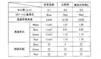
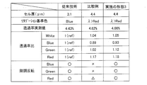
- the transmittance ratio of each color filter (specifically, each color from a certain white light source)
- the rightmost column of the table shown in FIG. 23 shows the transmittance ratio when the cell thickness is set based on B, G, and R.
- the transmittance ratio for the G reference (G optimum) and the R reference (R optimum) is shown with the transmittance in the case of the B reference (B optimum) being 100%.
- numerical values when digital ⁇ processing is not performed are shown in the upper table, and numerical values when digital ⁇ processing is performed are shown in the lower table. ing.
- the transmittance of the display image can be improved, in the case of image data supplied to light-colored pixels having a wavelength shorter than the reference wavelength when determining the cell thickness, the gradation is The problem is that reversal occurs.
- This gradation inversion is a phenomenon in which the transmittance of an image obtained with a low gradation value is higher than the transmittance of an image obtained with a high gradation value.
- the liquid crystal display device of the present invention is adapted to input image data for image data supplied to pixels having a light color shorter than the reference wavelength when the thickness of the liquid crystal layer is determined. It is preferable to have a gradation conversion unit that shifts the gradation value to a gradation value lower than the gradation value.
- the input gradation value is shifted to a lower gradation value than that value.
- gradation inversion occurs for the gradation value on the highest gradation side so that a gradation value equal to or higher than the gradation value that causes gradation inversion is not used. It is preferable to perform a gradation conversion process in which the gradation value is shifted to a gradation value lower than the gradation value and output.
- the gradation conversion unit performs a gradation value transition process that varies depending on the color type of the pixel.
- the transition processing of gradation values that differ depending on the type of pixel color means that, for example, even if the target gradation is the same (even if the input gradation is the same), the output gradation Is different for each color, and different gradation voltages for each color are supplied to the pixel electrodes. Further, when the gradation conversion process is performed using the lookup table, the gradation conversion process is performed using a different lookup table for each color.
- the liquid crystal display device includes a pseudo multi-gradation unit that performs a pseudo multi-gradation process on the image data that has been subjected to the gradation conversion process to the lower gradation value by the gradation conversion unit. It is preferable to have.
- the pseudo multi-gradation processing is performed on the image data on which the gradation value transition processing has been performed, thereby suppressing a decrease in gradation expression due to a decrease in the number of gradations to be used. be able to.
- the gradation conversion unit has a lookup table in which an input gradation value and an output gradation value are associated with each other.
- the gradation conversion process can be performed using the lookup table, the conversion process can be performed more easily. This simplifies the configuration of circuits and the like necessary for data conversion processing.
- the liquid crystal display panel includes pixels of three kinds of colors of blue, green, and red, and the thickness of the liquid crystal layer is based on the wavelength of green light or red light. It may be determined based on the retardation value.
- the cell thickness is determined based on the retardation value based on the wavelength of green or red having a wavelength larger than that of blue among the colors of the three types of pixels.
- the cell thickness can be set so that the transmittance is optimal with respect to the data.
- the liquid crystal display panel is composed of pixels of three kinds of colors, blue, green, and red, and the thickness of the liquid crystal layer has a retardation value based on the wavelength of green light. It may be determined on the basis.
- the human viewing angle is sensitive to green light and tends to feel brighter in terms of viewing angle when the transmittance of the green pixel increases.
- the thickness of the liquid crystal layer is determined so that the transmittance is optimal in the green pixel, it is possible to display an image that a person feels brighter.
- the liquid crystal display panel is composed of pixels of three kinds of colors of blue, green, and red, and the thickness of the liquid crystal layer is the wavelength of red light or the red light. It may be determined based on a retardation value based on a longer wavelength than the wavelength.
- the cell thickness can be made thicker than when the cell thickness is determined based on blue or green light. As the cell thickness decreases, the quality degradation due to contamination of dust becomes more significant. However, if the cell thickness is determined based on red light or light having a longer wavelength, the thickness decreases from 4.0 to It can be about 4.5 ⁇ m, and the cell thickness can be increased compared to the case where the cell thickness is set with reference to blue light, so that the deterioration of the panel quality due to contamination of dust etc. can be suppressed. it can.
- a driving method of a liquid crystal display device includes a liquid crystal display panel that includes a plurality of types of pixels having different colors and thereby performs color image display.
- the liquid crystal display panel is configured by sandwiching a liquid crystal layer between two substrates, and the thickness of the liquid crystal layer is the most among the wavelengths of light of the plurality of colors. It is determined on the basis of the retardation value based on light having a wavelength larger than that of light having a short wavelength, and the color of light having a wavelength shorter than that used as a reference when determining the thickness of the liquid crystal layer. It is characterized in that gradation conversion is performed on the supplied image data to shift the input gradation value to a gradation value lower than that value.
- the cell thickness is determined based on the retardation value based on light having a wavelength larger than the light having the shortest wavelength among the light wavelengths of the plurality of types of colors that the pixel has.
- the gradation value is shifted to the lower side for the image data supplied to the light-colored pixel having a wavelength shorter than the reference wavelength when determining the cell thickness. Yes.
- tone reversal can be prevented in pixels having a light wavelength shorter than the reference wavelength, and the quality of the display image can be improved.
- the driving method of the liquid crystal display device of the present invention it is preferable that in the step of performing the gradation conversion, a transition process of gradation values different depending on the color type of the pixel is performed.
- the driving method of the liquid crystal display device according to the present invention is a pseudo multi-gradation in which pseudo multi-gradation processing is performed on image data that has been subjected to gradation conversion processing to a lower gradation value by the above-described gradation conversion. It is preferable to include a conversion step.
- the gradation value is determined using a lookup table in which the input gradation value and the output gradation value are associated with each other. It is preferable to perform a migration process.
- the conversion process can be performed more easily. This simplifies the configuration of circuits and the like necessary for data conversion processing.
- the liquid crystal display panel is configured by sandwiching a liquid crystal layer between two substrates, and the thickness of the liquid crystal layer is the wavelength of each light of the plurality of colors.
- the retardation value is determined based on the retardation value based on light having a wavelength longer than the light having the shortest wavelength.
- the liquid crystal display device driving method is based on a retardation value based on light having a wavelength larger than the light having the shortest wavelength among the wavelengths of the light of the plurality of colors. For the image data supplied to the pixel of the light color having a shorter wavelength than the reference wavelength when the thickness of the liquid crystal layer is determined. Thus, gradation conversion is performed to shift the input gradation value to a gradation value lower than that value.
- the cell thickness is determined based on the retardation value based on light having a wavelength larger than the light having the shortest wavelength among the light wavelengths of the plurality of types of colors that the pixel has.
- (A) is a schematic diagram for demonstrating the display drive performed in the liquid crystal display device concerning the 1st Embodiment of this invention.
- (B) is a schematic diagram for demonstrating the display drive performed in the conventional liquid crystal display device. It is a block diagram which shows the structure of the liquid crystal display device concerning the 1st Embodiment of this invention. It is a graph which shows the (gamma) characteristic of the pixel of each color in case gradation reversal occurs. It is a graph which shows the transmittance
- FIG. 4 is a graph showing a relationship (tone transmission characteristic) between a gray level value and transmittance of blue image data in the liquid crystal display device according to the first embodiment of the present invention. It is a graph which shows the relationship between the light of each wavelength and the visibility in the liquid crystal display panel in the 1st Embodiment of this invention, and the conventional liquid crystal display panel.
- 5 is a table showing the results of evaluation of panel characteristics in the liquid crystal display device of the first embodiment of the present invention and the conventional liquid crystal display device.
- It is a block diagram which shows the structure of the liquid crystal display device concerning the 2nd Embodiment of this invention. It is a graph which shows the (gamma) characteristic of the pixel of each color in case gradation reversal occurs.
- the transmittance for each wavelength in the conventional liquid crystal display panel is indicated by a broken line.
- 6 is a table showing results of evaluating panel characteristics in a liquid crystal display device according to a second embodiment of the present invention and a conventional liquid crystal display device.
- It is a block diagram which shows the structure of the liquid crystal display device concerning the 3rd Embodiment of this invention.
- the transmittance for each wavelength in the conventional liquid crystal display panel is indicated by a broken line. It is a graph which shows the relationship (gradation transmittance
- the table shown at the top shows numerical values when digital ⁇ processing is not performed, and the table shown at the bottom shows numerical values when digital ⁇ processing is performed. It is a graph which shows the transmittance
- a liquid crystal display device provided with a TN mode liquid crystal display panel and provided with a polarizing plate so as to be normally white will be described as an example.
- the liquid crystal display device of this embodiment has a liquid crystal display panel composed of pixels of three kinds of colors of red (R), green (G), and blue (B), thereby displaying a color image. Is what you do.
- a pixel (pixel electrode) corresponding to a color filter of one color is defined as one pixel.
- FIG. 2 shows a configuration of the liquid crystal display device 10 of the present embodiment.
- the liquid crystal display device 10 includes, as main components, a liquid crystal display panel (LCD panel) 11, a gate driving circuit 12, a source driving circuit 13, a timing controller 14, and a display control circuit 15 (gradation conversion). Part).
- the liquid crystal display panel 11 has a configuration in which a liquid crystal layer is provided between an active matrix substrate and a counter substrate.
- the liquid crystal display panel 11 of the present embodiment is a TN mode.
- the liquid crystal display panel 11 is provided with one polarizing plate ( ⁇ / 2 plate) on the outside of the active matrix substrate and the counter substrate, and is driven to display normally white.
- the gate drive circuit 12 is a circuit for supplying a scanning signal to a scanning signal line provided on the liquid crystal display panel 11.
- the source drive circuit 13 is a circuit for supplying a data signal to a data signal line provided on the liquid crystal display panel 11.
- the timing controller 14 determines the input timing of each signal supplied to the scanning signal line and the data signal line provided in the liquid crystal display panel. Various signals output from the timing controller 14 are supplied to the scanning signal lines and the data signal lines of the liquid crystal display panel 11 through the gate driving circuit 12 and the source driving circuit 13.
- the display control circuit 15 performs data processing on the input video signals of each color (R, G, B) and supplies gradation data to the pixels of each color in the liquid crystal display panel 11.
- the gradation data processed in the display control circuit 15 is supplied to each pixel in the liquid crystal display panel 11 through the timing controller 14 and the source drive circuit 13. As a result, an image is displayed based on the input video signal.
- display data switching circuits 21, 22, and 23 are circuits that generate image data for performing a desired image display based on an input video signal.
- gradation conversion processing ⁇ conversion processing
- a lookup table is used when performing this gradation conversion processing.
- the look-up table is a table in which input gradation values and output gradation values are associated one-to-one.
- the display data switching circuit 21 and LUT 24 for the red video signal, the display data switching circuit 22 and LUT 25 for the green video signal, and the display data switching for the blue video signal are separately provided for each color video signal. Thereby, a different gradation conversion process can be performed for each color video signal.
- the display control circuit 15 is provided with a pseudo multi-gradation circuit 27 (pseudo multi-gradation unit) that performs pseudo multi-gradation processing on image data. Since the pseudo multi-gradation processing is performed only on the image data on which the gradation value shift processing is performed, in the present embodiment, the pseudo multi-gradation circuit 27 performs a series of processing on the blue image data. It is provided in the circuit.
- FIG. 1A schematically shows a flow of display driving performed in the liquid crystal display device 10.
- FIG. 1B schematically shows the flow of display driving performed in the conventional liquid crystal display device 500 for comparison.
- the cell thickness is determined so that the transmittance is optimal in the blue pixel having the shortest wavelength of RGB.
- the cell thickness is determined so that the transmittance is optimal in a green pixel having a wavelength longer than that of blue.
- the liquid crystal display panel is designed to obtain as high a transmittance as possible.
- the transmittance calculation formula of a normally white liquid crystal display panel using ⁇ / 2 plates on the upper and lower sides of the panel is as follows.
- the transmittance is determined by the light retardation value u.
- the retardation value u is calculated by the following equation 2.
- Equation 2 the retardation value u is determined by the birefringence of the liquid crystal material, the cell thickness, and the transmission wavelength. Therefore, when the liquid crystal material is determined, the cell thickness is selected such that a desired retardation value can be obtained at the reference transmission wavelength with a specific transmission wavelength as a reference.
- the transmittance calculation formula shown in (Formula 1) is a calculation formula for the liquid crystal layer.
- the transmittance of the liquid crystal display device depends on the transmittance obtained by (Equation 1) above, the transmittance of the polarizing plate, the transmittance of the color filter, the aperture ratio of the liquid crystal panel, and the concentration of the backlight. Calculated by multiplying the effects.
- the cell thickness is determined based on the retardation value based on the wavelength of blue light having the shortest wavelength among RGB. . This is because if the cell thickness is set based on a retardation value based on a wavelength longer than that of blue, in a pixel of a light color having a wavelength shorter than the reference wavelength, This is because gradation inversion is a problem.
- This gradation inversion is a phenomenon in which the transmittance of an image obtained with a low gradation value becomes higher than the transmittance of an image obtained with a high gradation value, which causes a reduction in display quality.
- FIG. 3 shows an example in which gradation inversion occurs.
- FIG. 3 shows gradation transmittance characteristics ( ⁇ characteristics) for each color when the cell thickness is designed to be 3.8 ⁇ m and the gradation characteristics are set based on white (RGB mixed color) light. As shown in FIG. 3, gradation inversion occurs in blue with the shortest wavelength.
- the cell thickness is determined based on the retardation value based on the wavelength of blue light having the shortest wavelength among RGB.
- the cell thickness is designed on the basis of the retardation value based on the shortest wavelength as in the liquid crystal display device 500, the green pixel and the red pixel are sufficient as shown in FIG. Therefore, it is impossible to obtain a sufficient transmittance.
- the cell thickness is set based on the wavelength of a color having a wavelength longer than that of blue so that the transmittance of green and red pixels is improved.
- the transmittance for each wavelength in the liquid crystal display device 10 in which the cell thickness is set based on the green wavelength is indicated by a solid line.
- the transmittance for each wavelength in the conventional liquid crystal display device 500 in which the cell thickness is set based on the blue wavelength is indicated by a broken line.
- the transmittance is maximum at a wavelength near blue (near 450 nm), and a wavelength near green (near 550 nm) to a wavelength near red (near 620 nm). As the wavelength increases, the transmittance decreases. In contrast, in the liquid crystal display device 10 of the present embodiment, the transmittance is maximum at a wavelength near green (near 550 nm), and the transmittance decreases as the distance from the wavelength increases. However, the degree of decrease in transmittance at a wavelength near red (near 620 nm) is smaller than that of the conventional liquid crystal display device 500. Therefore, the liquid crystal display device 10 can brighten the display as a whole as compared with the conventional liquid crystal display device 500.
- the cell thickness in the present embodiment for example, when the birefringence ⁇ n of the liquid crystal material is 0.130, the cell thickness d is 3.8 ⁇ m.
- the display control circuit 15 performs independent gradation value conversion ( ⁇ conversion) on the RGB video signals (see FIG. 1). ). This point will be described below with reference to FIGS.
- the gradation inversion phenomenon in the blue image data becomes a problem. Therefore, in the display data switching circuit 23, the input gradation value is lower than the value. A gradation value transition process for shifting to a gradation value is performed. The gradation conversion here is performed using the lookup table 26.
- red and green image data that does not undergo tone reversal is subjected to conversion processing similar to the conventional tone conversion processing. Also in this case, gradation conversion is performed using the lookup tables 24 and 25 provided corresponding to the display data switching circuits 21 and 22, respectively.
- FIG. 5 shows a relationship between the gradation value of the blue image data and the transmittance after the above-described gradation value transition processing in the liquid crystal display device 10.
- the gradation transmittance characteristic of the blue image data in the present embodiment is indicated by a solid line (no white circles), and the gradation transmittance characteristic of the blue image data when the gradation shift processing is not performed is a comparative example. As shown by a line with white circles.
- the high gradation side (gradation values 54 to 63) where gradation inversion can occur is shown in an enlarged manner.
- the liquid crystal display device 10 uses 58 gradations having the highest transmittance as 63 gradations. That is, in the display data switching circuit 23, when the input gradation value is 63 gradations, the gradation value is shifted to 58 gradations which are lower gradation values and output. It is carried out. In this way, the display data switching circuit 23 performs gradation value transition processing to the lower side such that the output gradation value is smaller than the input gradation value in all gradation regions.
- a pseudo multi-gradation circuit is provided in order to prevent gradation jump due to a decrease in the number of usable gradations by performing the gradation value transition process.
- 27 is used to interpolate gradation values.
- the image data is pseudo multi-gradation using a well-known multi-gradation technique.
- Pseudo multi-gradation processing uses the property that the human eye recognizes luminance by averaging time and space, so that the number of gradations that can be expressed to the human eye with a limited number of gradations. This is a process that seems to have increased.
- how large is the pixel area as a unit, or how the noise pattern is designed (that is, the noise pattern in each frame, the number of periodic frames, etc.) ), There are various methods such as FRC.
- Patent Document 2 Japanese Patent Laid-Open No. 2005-10520 (published on January 13, 2005) is also applied to the present invention. Can do.
- blue image data having gradation transmittance characteristics as shown in FIG. 5 can be obtained.
- the case of 6-bit (0 to 63 gradation) gradation data is shown, but this is an example, and the present invention is not limited to this.
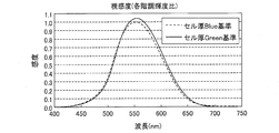
- FIG. 6 is a graph showing the relationship between light of each wavelength and visibility in the liquid crystal display device 10 of the present embodiment.
- the visibility in the liquid crystal display panel of the present embodiment is indicated by a solid line
- the cell thickness set on the basis of Blue is indicated by a broken line for comparison.
- the liquid crystal display device 10 has improved visibility as a whole centering on the wavelength of green light (near 550 nm) as compared with the conventional example indicated by the broken line. Yes.
- the human viewing angle has a high sensitivity to green light, and when the transmittance of the green pixel increases, the viewing angle tends to feel brighter.
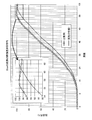
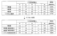
- FIG. 7 shows the result of evaluating the panel characteristics in the liquid crystal display device 10.
- a liquid crystal display panel in which the cell thickness is set with reference to blue light is shown as a prior art, and the cell thickness is set with reference to green light.
- a liquid crystal display panel that has not been subjected to the transition process is shown as a comparative example.
- the cell thickness is set based on blue light, and the thickness is 3.1 ⁇ m.
- the cell thickness is set based on the green light, so that it is thicker than the conventional panel and is 3.8 ⁇ m.
- the measured value of the white display transmittance of each panel is 4.43% in the conventional technique, whereas it is 4.92% in the comparative example and 5.01% in the first embodiment. It can be seen that the transmission is improved compared to the technical panel. Further, the transmittance ratio of each panel when the transmittance of white display (the portion indicated as “White” in FIG. 7) in the prior art panel is 1 (reference value) is 1.11 in the comparative example. It is 1.13 in Form 1. Thus, it can be seen that the transmittance of the liquid crystal display device of this embodiment is improved by 13% compared to the conventional liquid crystal display device.
- FIG. 7 also shows the transmittance ratio of each color display (shown as “Blue”, “Green”, and “Red” in FIG. 7).
- the lower part of the table shown in FIG. 7 indicates the presence or absence of gradation inversion (“ ⁇ ” indicates the presence of gradation inversion and “ ⁇ ” indicates the absence of gradation inversion).
- ⁇ indicates the presence of gradation inversion
- ⁇ indicates the absence of gradation inversion
- FIG. 23 shows simulation values of the luminance ratio for each color of the color filter and the transmittance ratio of the liquid crystal display device when the cell thickness is determined based on each of B, G, and R.
- numerical values when digital ⁇ processing is not performed are shown in the upper table, and numerical values when digital ⁇ processing is performed are shown in the lower table.
- the “G optimum” row in the lower table in FIG. 23 corresponds to the simulation value of the liquid crystal display device of the present embodiment. In an actual liquid crystal display device, this simulation value is combined with the influence of the backlight concentration and the polarizing plate.
- both the luminance (W) and the transmittance of W (white) obtained by mixing R, G, and B are both conventional (B optimum). It can be seen that this is an improvement compared to). As described above, it was confirmed that a higher transmittance can be obtained as a whole device by determining the cell thickness based on the longer wavelength green than the cell thickness determined based on the blue having the shortest wavelength.
- the cell thickness is set based on the retardation value based on the light of the green wavelength, not the blue of the shortest wavelength among the light wavelengths of RGB. Has been decided.
- the transmittance of the green pixel can be improved, but also the transmittance of the red pixel can be improved, and the transmittance of the entire image displayed by combining each color can also be improved.
- the cell thickness is determined so that the transmittance is optimal in the green pixel having high visibility, it is possible to display an image that makes a person feel brighter.
- the gradation value transition is such that the input gradation value is shifted to a gradation value lower than that value.
- a TN mode liquid crystal display panel has been described as an example.
- the present invention is not limited to this, and the present invention is applied to liquid crystal display panels of other modes such as an IPS mode and a VA mode. You can also.
- a normally white liquid crystal display panel has been described as an example.
- the present invention is not limited to this, and can be applied to a normally black liquid crystal display panel.
- Embodiment 2 Next, a second embodiment of the present invention will be described with reference to FIGS. Here, differences from Embodiment 1 described above will be mainly described, and description thereof will be omitted as appropriate when the same configuration and driving method can be applied.
- a liquid crystal display device including a TN mode liquid crystal display panel and having a polarizing plate disposed so as to be normally white will be described as an example.
- FIG. 8 shows a configuration of the liquid crystal display device 110 of the present embodiment.
- the liquid crystal display device 110 includes, as main components, a liquid crystal display panel (LCD panel) 11, a gate drive circuit 12, a source drive circuit 13, a timing controller 14, and a display control circuit 115 (tone conversion). Part).
- the liquid crystal display panel (LCD panel) 11, the gate drive circuit 12, the source drive circuit 13, and the timing controller 14 have the same configuration as the liquid crystal display device 10 of the first embodiment, the description thereof is omitted.
- the display control circuit 115 performs data processing on the input video signals of each color (R, G, B) and supplies gradation data to the pixels of each color in the liquid crystal display panel 11.
- the gradation data processed by the display control circuit 115 is supplied to each pixel in the liquid crystal display panel 11 via the timing controller 14 and the source driving circuit 13. As a result, an image is displayed based on the input video signal.
- display data switching circuits 121, 122, and 123 (gradation conversion units) and look-up tables (LUTs) 124, 125, and 126 are provided.
- the display data switching circuits 121, 122, and 123 are circuits that generate image data for performing a desired image display based on an input video signal.
- gradation conversion processing ⁇ conversion processing
- a lookup table is used when performing this gradation conversion processing.
- the look-up table is a table in which input gradation values and output gradation values are associated one-to-one.
- the display data switching circuit 121 and LUT 124 for the red video signal, the display data switching circuit 122 and LUT 125 for the green video signal, and the display data switching for the blue video signal are separately provided for each color video signal. Thereby, a different gradation conversion process can be performed for each color video signal.
- the display control circuit 115 is provided with pseudo multi-gradation circuits 127 and 128 (pseudo multi-gradation units) that perform pseudo multi-gradation processing on image data. Yes. Since the pseudo multi-gradation processing is performed only on the image data on which the gradation value shift processing is performed, in the present embodiment, the pseudo multi-gradation circuits 127 and 128 are configured so that the blue image data and green Are provided in a series of processing circuits for the image data.
- the cell thickness is determined so that the transmittance is optimal in the blue pixel having the shortest wavelength of RGB (see FIG. 1B).
- the wavelength of a color having a wavelength longer than that of blue is used as a reference so that the transmittance is improved in the green and red pixels.
- the cell thickness is set. Specifically, in this embodiment, the cell thickness is determined so that the transmittance is optimal in a red pixel having a longer wavelength than blue and green.
- the method described in the first embodiment can be similarly applied to the present embodiment.
- the red wavelength 620 nm is set as the reference transmission wavelength ⁇ .
- the cell thickness is selected so that the desired retardation value is obtained at the transmission wavelength.
- the transmittance for each wavelength in the liquid crystal display device 110 in which the cell thickness is set based on the red wavelength is indicated by a solid line.
- the transmittance for each wavelength in the conventional liquid crystal display device 500 in which the cell thickness is set based on the blue wavelength is indicated by a broken line.
- the transmittance is maximum at a wavelength near blue (near 450 nm), and a wavelength near green (near 550 nm) to a wavelength near red (near 620 nm). As the wavelength increases, the transmittance decreases.
- the transmittance is maximum at a wavelength near red (near 620 nm), and the transmittance decreases as the distance from the wavelength increases.
- the transmittance at a wavelength near green (approximately 550 nm) having the highest visibility among RGB is higher than that of the conventional liquid crystal display device 500. Therefore, the liquid crystal display device 110 can brighten the display as a whole as compared with the conventional liquid crystal display device 500.
- the cell thickness in the present embodiment for example, when the birefringence ⁇ n of the liquid crystal material is 0.130, the cell thickness d is 4.2 ⁇ m.
- the cell thickness is determined based on the red wavelength, as described in the first embodiment, there is a problem that gradation inversion occurs in blue and green pixels having wavelengths shorter than red.
- the cell thickness is set based on the Red standard, the cell thickness is designed to be 4.2 ⁇ m, and the grayscale transmittance for each color when the grayscale characteristics are set based on white (RGB mixed color) light. Characteristics ( ⁇ characteristics) are shown. As shown in FIG. 9, gradation inversion occurs in blue and green, which have shorter wavelengths than red.
- the display control circuit 115 performs independent gradation value conversion ( ⁇ conversion) for the RGB color video signals (FIG. 1 ( a)). This will be described below with reference to FIGS. 8, 11, and 12.
- FIG. 1 ( a) This will be described below with reference to FIGS. 8, 11, and 12.
- the gradation inversion phenomenon in the blue image data and the green image data becomes a problem, and therefore, the display data switching circuit 122 and the display data switching circuit 123 have the input floors.
- Gradation value transition processing is performed to shift the gradation value to a gradation value lower than that value.
- the gradation conversion here is performed using the lookup tables 125 and 126, respectively.
- gradation conversion is performed using the lookup table 124 provided corresponding to the display data switching circuit 121.
- FIG. 11 shows the relationship between the tone value of the blue image data and the transmittance after the tone value transition processing in the liquid crystal display device 110.
- the gradation transmittance characteristic of the blue image data in the present embodiment is indicated by a solid line (no white circle), and the gradation transmittance characteristic of the blue image data when the gradation shift process is not performed is a comparative example. As shown by a line with white circles.
- the upper left side of the graph shown in FIG. 11 is an enlarged view of the high gradation side (gradation values 54 to 63) where gradation inversion can occur.
- the liquid crystal display device 110 uses 57 gradations having the highest transmittance as 63 gradations. That is, in the display data switching circuit 123, when the input gradation value is 63 gradations, the gradation value is shifted to 57 gradations that are lower gradation values and output. It is carried out. As described above, the display data switching circuit 123 performs the gradation value transition processing to the lower side so that the output gradation value is smaller than the gradation value input in all gradation regions.
- FIG. 12 shows the relationship between the gradation value and the transmittance of the green image data after the gradation value transition process in the liquid crystal display device 110.
- the gradation transmittance characteristics of the green image data in the present embodiment are indicated by solid lines (no white circles), and the gradation transmittance characteristics of the green image data when the gradation shift processing is not performed are comparative examples. As shown by a line with white circles.
- the high gradation side (gradation values 54 to 63) where gradation inversion can occur is shown in an enlarged manner.
- gradation inversion occurs in a high gradation region of 61 gradations or more.
- 60 gradations having the highest transmittance are used as 63 gradations. That is, in the display data switching circuit 122, when the input gradation value is 63 gradations, the gradation value is shifted to 60 gradations that are lower gradation values and output. It is carried out. As described above, the display data switching circuit 122 performs gradation value transition processing to the lower side such that the output gradation value is smaller than the gradation value input in all gradation regions.
- the pseudo multi-gradation circuit is used to prevent the gradation jump due to the decrease in the number of usable gradations by performing the gradation value transition process.
- the gradation values are interpolated by 127 and 128.
- pseudo multi-gradation processing performed in the pseudo multi-gradation circuits 127 and 128 can be applied in the same manner as the method described in the first embodiment, the description thereof is omitted.
- blue image data having gradation transmittance characteristics as shown in FIG. 11 can be obtained, and a green image having gradation transmittance characteristics as shown in FIG. 12 can be obtained.
- Data can be obtained.
- FIGS. 11 and 12 the case of 6-bit (0 to 63 gradation) gradation data is shown, but this is an example, and the present invention is not limited to this.
- FIG. 13 is a graph showing the relationship between light of each wavelength and visibility in the liquid crystal display device 110 of the present embodiment.
- the visibility in the liquid crystal display panel of this embodiment is indicated by a solid line
- the cell thickness set on the basis of Blue is indicated by a broken line for comparison.
- the liquid crystal display device 110 has improved visibility as a whole, centering on the wavelength of red light (near 620 nm), as compared with the conventional example indicated by the broken line. Yes.
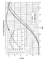
- FIG. 14 shows the result of evaluating the panel characteristics in the liquid crystal display device 110.
- a liquid crystal display panel in which the cell thickness is set with reference to blue light is shown as a prior art, and the cell thickness is set with reference to red light.
- a liquid crystal display panel that has not been subjected to the transition process is shown as a comparative example.
- the cell thickness is set based on blue light, and the thickness is 3.1 ⁇ m.
- the cell thickness is set based on the red light, so that it is thicker than the panel of the prior art and is 4.2 ⁇ m.
- the measured value of the transmittance of white display of each panel is 4.43% in the comparative example and 4.83% in the second embodiment compared to 4.43% in the conventional technique. It can be seen that the transmission is improved compared to the technical panel. Further, the transmittance ratio of each panel when the transmittance of white display (the portion indicated as “White” in FIG. 14) in the prior art panel is 1 (reference value) is 1.07 in the comparative example. It is 1.09 in Form 2. Thus, it can be seen that the transmittance of the liquid crystal display device of the present embodiment is improved by 9% compared to the conventional liquid crystal display device.
- FIG. 14 also shows the transmittance ratio of each color display (shown as “Blue”, “Green”, and “Red” in FIG. 14).
- the lower part of the table shown in FIG. 14 indicates the presence or absence of gradation inversion (“ ⁇ ” indicates that there is gradation inversion, and “ ⁇ ” indicates that there is no gradation inversion).
- ⁇ indicates that there is gradation inversion
- ⁇ indicates that there is no gradation inversion
- the gradation inversion occurs in the blue and green images, whereas the gradation value transition processing is performed on the blue and green image data.
- gradation inversion does not occur. This is considered to be reflected in the transmittance ratio of blue display and green display, the transmittance ratio of white display, and the measured value of transmittance.
- FIG. 23 shows simulation values of the luminance ratio for each color of the color filter and the transmittance ratio of the liquid crystal display device when the cell thickness is determined based on each of B, G, and R.
- numerical values when digital ⁇ processing is not performed are shown in the upper table, and numerical values when digital ⁇ processing is performed are shown in the lower table.
- the “R optimum” row in the lower table in FIG. 23 corresponds to the simulation value of the liquid crystal display device of the present embodiment. In an actual liquid crystal display device, this simulation value is combined with the influence of the backlight concentration and the polarizing plate.
- both the luminance (W) and the transmittance of W (white) obtained by mixing R, G, and B are conventional (B optimal) It can be seen that this is an improvement compared to). As described above, it was confirmed that a higher transmittance can be obtained as a whole device by determining the cell thickness based on the longer wavelength red than the cell thickness determined based on the shortest blue wavelength.
- the cell thickness is set based on the retardation value based on the light of the red wavelength, not the blue of the shortest wavelength among the light wavelengths of the RGB colors. Has been decided. Thereby, not only the transmittance of the red pixel can be improved, but also the transmittance of the green pixel can be improved, and the transmittance of the entire image displayed by combining each color can also be improved.
- the cell thickness when the cell thickness is set based on red, the cell thickness can be increased compared to the case where the cell thickness is set based on blue or green. Therefore, the effect that the durability of the liquid crystal display panel against the entry of foreign matters such as dust can be improved is obtained.
- the gradation value that shifts the input gradation value to a gradation value lower than that value By performing this transition process, it is possible to prevent gradation inversion in the blue and green pixels. Thereby, the quality of a display image can be improved.
- Embodiment 3 Next, a third embodiment of the present invention will be described with reference to FIGS. Here, differences from Embodiment 1 described above will be mainly described, and description thereof will be omitted as appropriate when the same configuration and driving method can be applied.
- a liquid crystal display device including a TN mode liquid crystal display panel and having a polarizing plate disposed so as to be normally white will be described as an example.
- FIG. 15 shows a configuration of the liquid crystal display device 210 of the present embodiment.
- the liquid crystal display device 210 includes, as main components, a liquid crystal display panel (LCD panel) 11, a gate drive circuit 12, a source drive circuit 13, a timing controller 14, a display control circuit 215 (gradation conversion). Part).
- the liquid crystal display panel (LCD panel) 11, the gate drive circuit 12, the source drive circuit 13, and the timing controller 14 have the same configuration as the liquid crystal display device 10 of the first embodiment, the description thereof is omitted.
- the display control circuit 215 performs data processing on the input video signals of each color (R, G, B) and supplies gradation data to each color pixel in the liquid crystal display panel 11.
- the gradation data processed by the display control circuit 215 is supplied to each pixel in the liquid crystal display panel 11 through the timing controller 14 and the source drive circuit 13. As a result, an image is displayed based on the input video signal.
- display data switching circuits 221, 222, and 223 (gradation conversion units) and look-up tables (LUT) 224, 225, and 226 are provided.
- the display data switching circuits 221, 222, and 223 are circuits that generate image data for performing a desired image display based on the input video signal.
- gradation conversion processing ⁇ conversion processing
- a lookup table is used when performing this gradation conversion processing.
- the look-up table is a table in which input gradation values and output gradation values are associated one-to-one.
- the display data switching circuit 221 and LUT 224 for the red video signal, the display data switching circuit 222 and LUT 225 for the green video signal, and the display data switching for the blue video signal are provided separately for each color video signal. Thereby, a different gradation conversion process can be performed for each color video signal.
- the display control circuit 215 includes pseudo multi-gradation circuits 227, 228, and 229 (pseudo multi-gradation units) that perform pseudo multi-gradation processing on image data. It has been.
- the pseudo multi-gradation processing is performed on the image data on which the gradation value transition processing is performed. In the present embodiment, this transition processing is performed on the image data of all the RGB colors.
- the multi-gradation circuits 227, 228, and 229 are provided in a series of processing circuits for blue image data, green image data, and red image data, respectively.
- the cell thickness is determined so that the transmittance is optimal in the blue pixel having the shortest wavelength of RGB (see FIG. 1B).
- the wavelength of a color having a wavelength longer than that of blue is used as a reference so that the transmittance is improved in green and red pixels.
- the cell thickness is set. Specifically, in this embodiment, the cell thickness is determined so that the transmittance is optimal for light having a longer wavelength than red light (light having a wavelength of 670 nm).
- the method described in the first embodiment can be similarly applied to the present embodiment.
- 670 nm is set as a reference transmission wavelength ⁇ , and this reference transmission wavelength is set.
- the cell thickness is selected so that the desired retardation value can be obtained.
- the transmittance for each wavelength in the liquid crystal display device 210 in which the cell thickness is set based on the wavelength of 670 nm is indicated by a solid line. Further, in FIG. 17, the transmittance for each wavelength in the conventional liquid crystal display device 500 in which the cell thickness is set with reference to the blue wavelength is indicated by a broken line.
- the transmittance is maximum at a wavelength near blue (near 450 nm), and a wavelength near green (near 550 nm) to a wavelength near red (near 620 nm). As the wavelength increases, the transmittance decreases. On the other hand, in the liquid crystal display device 210 of the present embodiment, the transmittance is maximum at a wavelength longer than the red light (near 670 nm), and the transmittance decreases with increasing distance from this wavelength. ing.
- the cell thickness in the present embodiment for example, when the birefringence ⁇ n of the liquid crystal material is 0.130, the cell thickness d is 4.4 ⁇ m.
- the cell thickness is determined based on the wavelength of 670 nm, as described in the first embodiment, there is a problem that gradation inversion occurs in pixels of each RGB color shorter than this wavelength.
- the cell thickness is set with reference to a wavelength longer than Red (specifically, a wavelength of 670 nm), the cell thickness is designed to be 4.4 ⁇ m, and white (RGB mixed color) light is emitted.
- the gradation transmittance characteristic ( ⁇ characteristic) for each color when the gradation characteristic is set as a reference is shown. As shown in FIG. 16, gradation inversion occurs in blue, green, and red image data having wavelengths shorter than 670 nm.
- the display control circuit 215 performs independent gradation value conversion ( ⁇ conversion) for the RGB video signals (FIG. 1 (FIG. 1 (FIG. 1)). a)). This point will be described below with reference to FIGS. 15, 18, 19, and 20.
- FIG. 1 gradation value conversion
- the gradation inversion phenomenon in each of the blue, green, and red image data becomes a problem. Therefore, the display data switching circuits 221, 222, and 223 for the video signals of the respective colors are input. Gradation value transition processing is performed in which the gradation value thus transferred is shifted to a gradation value lower than that value. The gradation conversion here is performed using the look-up tables 224, 225, and 226, respectively.
- FIG. 18 shows the relationship between the tone value of the blue image data and the transmittance after the above-described tone value transition processing in the liquid crystal display device 210.
- the gradation transmittance characteristic of the blue image data in the present embodiment is indicated by a solid line (no white circles), and the gradation transmittance characteristic of the blue image data when the gradation shift processing is not performed is a comparative example. As shown by a line with white circles.
- the high gradation side (gradation values 54 to 63) where gradation inversion can occur is shown in an enlarged manner.
- the liquid crystal display device 210 uses 58 gradations having the highest transmittance as 63 gradations. That is, in the display data switching circuit 223, when the input gradation value is 63 gradations, the gradation value is shifted to 58 gradations which are lower gradation values and output. It is carried out. As described above, the display data switching circuit 223 performs gradation value transition processing to the lower side such that the output gradation value is smaller than the gradation value input in all gradation regions.
- FIG. 19 shows the relationship between the gradation value of the green image data and the transmittance after the above-described gradation value transition processing in the liquid crystal display device 210.
- the gradation transmittance characteristic of the green image data in the present embodiment is indicated by a solid line (no white circles), and the gradation transmittance characteristic of the green image data in the case where the gradation shift process is not performed is a comparative example. As shown by a line with white circles.
- the high gradation side (gradation values 54 to 63) where gradation inversion can occur is shown in an enlarged manner.
- gradation inversion occurs in a high gradation region of 61 gradations or more.
- 60 gradations having the highest transmittance are used as 63 gradations. That is, in the display data switching circuit 222, when the input gradation value is 63 gradations, the gradation value is shifted to 60 gradations that are lower gradation values and output. It is carried out. As described above, the display data switching circuit 222 performs gradation value transition processing to the lower side such that the output gradation value is smaller than the gradation value input in all gradation regions.
- FIG. 20 shows the relationship between the tone value and the transmittance of the red image data after the above tone value transition processing in the liquid crystal display device 210.
- the gradation transmittance characteristic of the red image data in the present embodiment is indicated by a solid line (no white circles), and the gradation transmittance characteristic of the red image data when the gradation shift processing is not performed is a comparative example. As shown by a line with white circles.
- the high gradation side (gradation values 57 to 63) where gradation inversion can occur is shown in an enlarged manner.
- gradation inversion occurs at 63 gradations having the highest gradation value.
- 62 gradations having the highest transmittance are used as 63 gradations. That is, in the display data switching circuit 221, when the input gradation value is 63 gradations, the gradation value is shifted to 62 gradations that are lower gradation values and output. It is carried out. As described above, the display data switching circuit 221 performs gradation value transition processing to the lower side such that the output gradation value is smaller than the gradation value input in all gradation regions.
- a pseudo multi-gradation circuit is provided in order to prevent gradation skip due to a decrease in the number of usable gradations by performing the above-described gradation value transition processing.
- the gradation values are interpolated by 227, 228, and 229.
- the pseudo multi-gradation processing performed in the pseudo multi-gradation circuits 227, 228, and 229 can be applied in the same manner as the method described in the first embodiment, and thus the description thereof is omitted.
- gradation transmittance characteristics as shown in FIGS. 18, 19, and 20 can be obtained for each of the blue, green, and red image data.
- the examples shown in FIGS. 18, 19, and 20 show the case of 6-bit (0 to 63 gradation) gradation data, but this is an example, and the present invention is not limited to this. .
- FIG. 21 is a graph showing the relationship between the light of each wavelength and the visibility in the liquid crystal display device 210 of the present embodiment.
- the visibility in the liquid crystal display panel of the present embodiment is shown by a solid line
- the cell thickness set on the basis of Blue is shown by a broken line for comparison.
- the liquid crystal display device 210 of the present embodiment has improved overall visibility compared to the conventional example indicated by the broken line. This is because, as shown in FIG. 23, the transmittance of green and red can be improved by using the wavelength of 670 nm as a reference for determining the cell thickness.
- FIG. 22 shows the result of evaluating the panel characteristics in the liquid crystal display device 210.
- a liquid crystal display panel in which the cell thickness is set with reference to blue light is shown as a conventional technique, and light with a wavelength longer than red (specifically, 670 nm) is used as a reference.
- a liquid crystal display panel in which the cell thickness is set but the gradation value transition process is not performed is shown as a comparative example.
- the cell thickness is set based on blue light, and the thickness is 3.1 ⁇ m.
- the cell thickness is set based on the light of 670 nm, so that it is thicker than the panel of the prior art and is 4.4 ⁇ m.
- the measured value of the white display transmittance of each panel is 4.43% in the comparative example, while it is 4.62% in the comparative example and 4.66% in the third embodiment. It can be seen that the transmission is improved compared to the technical panel. Further, the transmittance ratio of each panel when the transmittance of white display in the prior art panel (location shown as “White” in FIG. 22) is 1 (reference value) is 1.04 in the comparative example. It is 1.05 in Form 3. Thus, it can be seen that the transmittance of the liquid crystal display device of the present embodiment is improved by 5% compared to the conventional liquid crystal display device.
- FIG. 22 also shows the transmittance ratio of each color display (shown as “Blue”, “Green”, and “Red” in FIG. 22).
- the lower part of the table shown in FIG. 22 indicates the presence or absence of gradation inversion (“ ⁇ ” indicates that there is gradation inversion and “ ⁇ ” indicates that there is no gradation inversion).
- ⁇ indicates that there is gradation inversion
- ⁇ indicates that there is no gradation inversion
- the gradation inversion occurs in the image of three colors of blue, green, and red, whereas the transition of the gradation value is performed in the panel of the third embodiment. Then, gradation inversion has not occurred. This is considered to be reflected in the transmittance ratio of each color display, the transmittance ratio of white display, and the measured value of the transmittance.
- FIG. 23 shows simulation values of the luminance ratio for each color of the color filter and the transmittance ratio of the liquid crystal display device when the cell thickness is determined based on each of B, G, and R.
- numerical values when digital ⁇ processing is not performed are shown in the upper table, and numerical values when digital ⁇ processing is performed are shown in the lower table.
- both the luminance (W) and the transmittance of W (white) obtained by mixing R, G, and B are conventional examples ( It can be seen that it is improved as compared with (B optimum). In this way, it is confirmed that it is possible to obtain a higher transmittance as a whole device by determining the cell thickness based on the longer wavelength of 670 nm rather than determining the cell thickness based on the shortest blue wavelength. It was.
- the retardation value based on light having a wavelength longer than red is used as a reference, instead of blue having the shortest wavelength among the wavelengths of light of RGB colors.
- the cell thickness is determined.
- the cell thickness when the cell thickness is set based on light having a wavelength longer than red, the cell thickness may be increased compared to the case where the cell thickness is set based on blue or green. it can. Therefore, the effect that the durability of the liquid crystal display panel against the entry of foreign matters such as dust can be improved is obtained.
- the input gradation value is shifted to a lower gradation value than that value.
- the transmittance of the display image can be improved.
- the liquid crystal display device of the present invention can be applied to a color liquid crystal display device.
Abstract
Description
上記の式において、Δn:液晶材料の屈折率異方性(複屈折)
d:セル厚
λ:光の波長
上記の式より、液晶表示パネルの液晶層の厚さ(セル厚とも呼ぶ)は、液晶材料の種類によって決まる屈折率異方性Δn、基準とする光の波長λ、および目的とする透過率を得るためのリタデーション値uから決定される。 u = 2 · Δnd / λ
In the above formula, Δn: refractive index anisotropy (birefringence) of the liquid crystal material
d: cell thickness λ: wavelength of light From the above formula, the thickness of the liquid crystal layer of the liquid crystal display panel (also referred to as cell thickness) is the refractive index anisotropy Δn determined by the type of liquid crystal material, the wavelength of the reference light It is determined from λ and the retardation value u for obtaining the desired transmittance.
本発明の第1の実施形態について図1~図7に基づいて説明すると以下の通りである。なお、本発明はこれに限定されるものではない。 [Embodiment 1]
A first embodiment of the present invention will be described below with reference to FIGS. Note that the present invention is not limited to this.
図2に示すように、液晶表示装置10は、主な構成部材として、液晶表示パネル(LCDパネル)11、ゲート駆動回路12、ソース駆動回路13、タイミングコントローラ14、表示制御回路15(階調変換部)などを備えている。 FIG. 2 shows a configuration of the liquid
As shown in FIG. 2, the liquid

ここで、Δn:液晶材料の複屈折
d:セル厚
λ:透過波長
上記の式2に示すように、リタデーション値uは、液晶材料の複屈折、セル厚、および、透過波長によって決定される。そのため、液晶材料が決まっている場合には、ある特定の透過波長を基準とし、この基準となる透過波長において所望とするリタデーション値が得られるようなセル厚が選択されることになる。 u = 2Δnd / λ (Formula 2)
Here, Δn: birefringence of the liquid crystal material d: cell thickness λ: transmission wavelength As shown in Equation 2 above, the retardation value u is determined by the birefringence of the liquid crystal material, the cell thickness, and the transmission wavelength. Therefore, when the liquid crystal material is determined, the cell thickness is selected such that a desired retardation value can be obtained at the reference transmission wavelength with a specific transmission wavelength as a reference.
次に、本発明の第2の実施形態について図8~図14に基づいて説明する。ここでは、主に上述した実施の形態1とは異なる点について説明し、同様の構成および駆動方法が適用できる場合には、その説明を適宜省略する。 [Embodiment 2]
Next, a second embodiment of the present invention will be described with reference to FIGS. Here, differences from
図8に示すように、液晶表示装置110は、主な構成部材として、液晶表示パネル(LCDパネル)11、ゲート駆動回路12、ソース駆動回路13、タイミングコントローラ14、表示制御回路115(階調変換部)などを備えている。 FIG. 8 shows a configuration of the liquid
As shown in FIG. 8, the liquid
次に、本発明の第3の実施形態について図15~図22に基づいて説明する。ここでは、主に上述した実施の形態1とは異なる点について説明し、同様の構成および駆動方法が適用できる場合には、その説明を適宜省略する。 [Embodiment 3]
Next, a third embodiment of the present invention will be described with reference to FIGS. Here, differences from
図15に示すように、液晶表示装置210は、主な構成部材として、液晶表示パネル(LCDパネル)11、ゲート駆動回路12、ソース駆動回路13、タイミングコントローラ14、表示制御回路215(階調変換部)などを備えている。 FIG. 15 shows a configuration of the liquid crystal display device 210 of the present embodiment.
As shown in FIG. 15, the liquid crystal display device 210 includes, as main components, a liquid crystal display panel (LCD panel) 11, a
11 液晶表示パネル
12 ゲート駆動回路
13 ソース駆動回路
14 タイミングコントローラ
15 表示制御回路(階調変換部)
21・22・23 表示データ切替え回路(階調変換部)
24・25・26 ルックアップテーブル(LUT)
27 擬似多階調化回路(擬似多階調化部)
110 液晶表示装置
115 表示制御回路(階調変換部)
121・122・123 表示データ切替え回路(階調変換部)
124・125・126 ルックアップテーブル(LUT)
127・128 擬似多階調化回路(擬似多階調化部)
210 液晶表示装置
215 表示制御回路(階調変換部)
221・222・223 表示データ切替え回路(階調変換部)
224・225・226 ルックアップテーブル(LUT)
227・228・229 擬似多階調化回路(擬似多階調化部)
d セル厚(液晶層の厚さ)
u リタデーション値 DESCRIPTION OF
21, 22, 23 Display data switching circuit (gradation converter)
24 ・ 25 ・ 26 Lookup Table (LUT)
27 Pseudo multi-gradation circuit (pseudo multi-gradation part)
110 Liquid
121, 122, 123 Display data switching circuit (gradation converter)
124, 125, 126 Look-up table (LUT)
127/128 Pseudo multi-gradation circuit (pseudo multi-gradation part)
210 Liquid crystal display device 215 Display control circuit (gradation converter)
221/222/223 Display data switching circuit (gradation converter)
224/225/226 Look-up table (LUT)
227/228/229 Pseudo multi-gradation circuit (pseudo multi-gradation unit)
d Cell thickness (thickness of liquid crystal layer)
u Retardation value
Claims (12)
- 互いに色の異なる複数種類の画素を有し、これによってカラー画像表示を行う液晶表示パネルを備えている液晶表示装置であって、
上記液晶表示パネルは、2枚の基板の間に液晶層を挟んで構成されており、
上記液晶層の厚さは、上記複数種類の色の各光の波長のうちで最も短い波長の光よりも大きな波長の光に基づくリタデーション値を基準にして決定されていることを特徴とする液晶表示装置。 A liquid crystal display device having a plurality of types of pixels having different colors and having a liquid crystal display panel for performing color image display,
The liquid crystal display panel is configured by sandwiching a liquid crystal layer between two substrates,
The thickness of the liquid crystal layer is determined based on a retardation value based on light having a wavelength larger than the light having the shortest wavelength among the light wavelengths of the plurality of types of colors. Display device. - 上記液晶層の厚さの決定をするときに基準とした波長よりも短波長の光の色の画素に供給される画像データに対して、入力された階調値をその値よりも下位側の階調値へ移行させる階調変換部を有していることを特徴とする請求項1に記載の液晶表示装置。 For the image data supplied to the pixel of the light color having a shorter wavelength than the reference wavelength when determining the thickness of the liquid crystal layer, the input gradation value is lower than that value. The liquid crystal display device according to claim 1, further comprising a gradation conversion unit that shifts to a gradation value.
- 上記階調変換部は、上記画素の色の種類によって異なる階調値の移行処理を行うことを特徴とする請求項2に記載の液晶表示装置。 3. The liquid crystal display device according to claim 2, wherein the gradation conversion unit performs a gradation value transition process depending on a color type of the pixel.
- 上記階調変換部によって下位側の階調値への階調変換処理を行った画像データに対して、擬似多階調化処理を行う擬似多階調化部を有していることを特徴とする請求項2または3に記載の液晶表示装置。 The image processing apparatus has a pseudo multi-gradation unit that performs pseudo multi-gradation processing on image data that has been subjected to gradation conversion processing to a lower gradation value by the gradation conversion unit. The liquid crystal display device according to claim 2.
- 上記階調変換部は、入力される階調値と出力される階調値とをそれぞれ対応付けたルックアップテーブルを有していることを特徴とする請求項2~4の何れか1項に記載の液晶表示装置。 5. The gradation conversion unit according to claim 2, wherein the gradation conversion unit includes a look-up table in which input gradation values and output gradation values are associated with each other. The liquid crystal display device described.
- 上記液晶表示パネルは、青色、緑色、および赤色の3種類の色の画素で構成されており、
上記液晶層の厚さは、緑色光または赤色光の波長に基づくリタデーション値を基準にして決定されていることを特徴とする請求項1~5の何れか1項に記載の液晶表示装置。 The liquid crystal display panel is composed of pixels of three kinds of colors, blue, green and red,
6. The liquid crystal display device according to claim 1, wherein the thickness of the liquid crystal layer is determined based on a retardation value based on a wavelength of green light or red light. - 上記液晶表示パネルは、青色、緑色、および赤色の3種類の色の画素で構成されており、
上記液晶層の厚さは、緑色光の波長に基づくリタデーション値を基準にして決定されていることを特徴とする請求項1~5の何れか1項に記載の液晶表示装置。 The liquid crystal display panel is composed of pixels of three kinds of colors, blue, green and red,
6. The liquid crystal display device according to claim 1, wherein the thickness of the liquid crystal layer is determined based on a retardation value based on a wavelength of green light. - 上記液晶表示パネルは、青色、緑色、および赤色の3種類の色の画素で構成されており、
上記液晶層の厚さは、赤色光の波長または該赤色光の波長よりも長波長に基づくリタデーション値を基準にして決定されていることを特徴とする請求項1~5の何れか1項に記載の液晶表示装置。 The liquid crystal display panel is composed of pixels of three kinds of colors, blue, green and red,
6. The liquid crystal layer according to claim 1, wherein the thickness of the liquid crystal layer is determined based on a retardation value based on a wavelength of red light or a wavelength longer than the wavelength of red light. The liquid crystal display device described. - 互いに色の異なる複数種類の画素を有し、これによってカラー画像表示を行う液晶表示パネルを備えている液晶表示装置の駆動方法であって、
上記液晶表示パネルは、2枚の基板の間に液晶層を挟んで構成され、
上記液晶層の厚さは、上記複数種類の色の各光の波長のうちで最も短い波長の光よりも大きな波長の光に基づくリタデーション値を基準にして決定されており、
上記液晶層の厚さの決定をするときに基準とした波長よりも短波長の光の色の画素に供給される画像データに対して、入力された階調値をその値よりも下位側の階調値へ移行させる階調変換を行うことを特徴とする駆動方法。 A method for driving a liquid crystal display device having a liquid crystal display panel having a plurality of types of pixels of different colors and thereby performing color image display,
The liquid crystal display panel is configured by sandwiching a liquid crystal layer between two substrates,
The thickness of the liquid crystal layer is determined based on a retardation value based on light having a wavelength larger than the light having the shortest wavelength among the light wavelengths of the plurality of colors.
For the image data supplied to the pixel of the light color having a shorter wavelength than the reference wavelength when determining the thickness of the liquid crystal layer, the input gradation value is lower than that value. A driving method characterized by performing gradation conversion for shifting to a gradation value. - 上記の階調変換を行う工程では、上記画素の色の種類によって異なる階調値の移行処理を行うことを特徴とする請求項9に記載の駆動方法。 10. The driving method according to claim 9, wherein in the step of performing the gradation conversion, a transition process of a gradation value that varies depending on a color type of the pixel is performed.
- 上記の階調変換によって下位側の階調値への階調変換処理を行った画像データに対して、擬似多階調化処理を行う擬似多階調化工程を含むことを特徴とする請求項9または10に記載の駆動方法。 5. A pseudo multi-gradation process for performing a pseudo multi-gradation process on image data that has been subjected to a gradation conversion process to a lower gradation value by the gradation conversion described above. The driving method according to 9 or 10.
- 上記の階調変換を行う工程では、入力される階調値と出力される階調値とをそれぞれ対応付けたルックアップテーブルを用いて階調値の移行処理を行うことを特徴とする請求項9~11の何れか1項に記載の駆動方法。 The gradation value transfer process is performed using a lookup table in which an input gradation value and an output gradation value are associated with each other in the gradation conversion step. The driving method according to any one of 9 to 11.
Priority Applications (6)
| Application Number | Priority Date | Filing Date | Title |
|---|---|---|---|
| BRPI0921574A BRPI0921574A2 (en) | 2008-11-19 | 2009-08-27 | liquid crystal display device and method to trigger the same |
| JP2010539180A JPWO2010058644A1 (en) | 2008-11-19 | 2009-08-27 | Liquid crystal display device and driving method of liquid crystal display device |
| EP09827425A EP2365382A4 (en) | 2008-11-19 | 2009-08-27 | Liquid crystal display device and method for driving liquid crystal display device |
| CN200980145490.1A CN102216835B (en) | 2008-11-19 | 2009-08-27 | Liquid crystal display device and method for driving liquid crystal display device |
| US12/998,665 US8605020B2 (en) | 2008-11-19 | 2009-08-27 | Liquid crystal display device and method for driving same |
| RU2011124247/28A RU2011124247A (en) | 2008-11-19 | 2009-08-27 | LIQUID CRYSTAL DISPLAY DEVICE AND METHOD OF ITS EXCITATION |
Applications Claiming Priority (2)
| Application Number | Priority Date | Filing Date | Title |
|---|---|---|---|
| JP2008-295720 | 2008-11-19 | ||
| JP2008295720 | 2008-11-19 |
Publications (1)
| Publication Number | Publication Date |
|---|---|
| WO2010058644A1 true WO2010058644A1 (en) | 2010-05-27 |
Family
ID=42198083
Family Applications (1)
| Application Number | Title | Priority Date | Filing Date |
|---|---|---|---|
| PCT/JP2009/064988 WO2010058644A1 (en) | 2008-11-19 | 2009-08-27 | Liquid crystal display device and method for driving liquid crystal display device |
Country Status (7)
| Country | Link |
|---|---|
| US (1) | US8605020B2 (en) |
| EP (1) | EP2365382A4 (en) |
| JP (1) | JPWO2010058644A1 (en) |
| CN (1) | CN102216835B (en) |
| BR (1) | BRPI0921574A2 (en) |
| RU (1) | RU2011124247A (en) |
| WO (1) | WO2010058644A1 (en) |
Cited By (1)
| Publication number | Priority date | Publication date | Assignee | Title |
|---|---|---|---|---|
| CN102456335A (en) * | 2010-10-26 | 2012-05-16 | 乐金显示有限公司 | Liquid crystal display device and driving method of the same |
Families Citing this family (4)
| Publication number | Priority date | Publication date | Assignee | Title |
|---|---|---|---|---|
| US8847864B2 (en) | 2011-11-24 | 2014-09-30 | Shenzhen China Star Optoelectronics Technology Co., Ltd. | Color flat display panel and corresponding color flat display device having gamma reference voltages for red, green and blue colors |
| CN102411914B (en) * | 2011-11-24 | 2013-07-10 | 深圳市华星光电技术有限公司 | Colored planar display panel and corresponding colored planar display device |
| US9384689B2 (en) * | 2012-07-30 | 2016-07-05 | Sharp Kabushiki Kaisha | Viewing angle characteristic improving method in liquid crystal display device, and liquid crystal display device |
| US9940864B2 (en) * | 2014-06-25 | 2018-04-10 | Sharp Kabushiki Kaisha | Display device and method for driving same |
Citations (6)
| Publication number | Priority date | Publication date | Assignee | Title |
|---|---|---|---|---|
| JPS6198330A (en) | 1984-10-19 | 1986-05-16 | Seiko Epson Corp | Multicolor liquid crystal display device |
| JPH07199173A (en) * | 1993-12-02 | 1995-08-04 | Ois Opt Imaging Syst Inc | Liquid crystal display, picture element and manufacture thereof |
| JPH07281176A (en) * | 1994-02-18 | 1995-10-27 | Fujitsu Ltd | Liquid crystal display panel |
| JPH09160019A (en) * | 1995-12-11 | 1997-06-20 | Fujitsu Ltd | Color liquid crystal display panel |
| JP2005010520A (en) | 2003-06-19 | 2005-01-13 | Sharp Corp | Liquid crystal halftone display method and liquid crystal display device using same method |
| JP2007279276A (en) * | 2006-04-05 | 2007-10-25 | Epson Imaging Devices Corp | Liquid crystal device and electronic equipment |
Family Cites Families (6)
| Publication number | Priority date | Publication date | Assignee | Title |
|---|---|---|---|---|
| JP3277121B2 (en) | 1996-05-22 | 2002-04-22 | インターナショナル・ビジネス・マシーンズ・コーポレーション | Intermediate display drive method for liquid crystal display |
| JP2001281619A (en) | 2000-03-28 | 2001-10-10 | Sanyo Electric Co Ltd | Color liquid crystal display device |
| JP3796499B2 (en) * | 2002-11-06 | 2006-07-12 | キヤノン株式会社 | Color display element, color display element driving method, and color display device |
| KR100608814B1 (en) * | 2004-07-16 | 2006-08-08 | 엘지전자 주식회사 | Method for displaying image data in lcd |
| JP2007033864A (en) * | 2005-07-27 | 2007-02-08 | Mitsubishi Electric Corp | Image processing circuit and image processing method |
| CN101192382B (en) * | 2006-11-29 | 2010-11-10 | 群康科技(深圳)有限公司 | LCD device |
-
2009
- 2009-08-27 BR BRPI0921574A patent/BRPI0921574A2/en not_active IP Right Cessation
- 2009-08-27 CN CN200980145490.1A patent/CN102216835B/en not_active Expired - Fee Related
- 2009-08-27 JP JP2010539180A patent/JPWO2010058644A1/en active Pending
- 2009-08-27 RU RU2011124247/28A patent/RU2011124247A/en not_active Application Discontinuation
- 2009-08-27 US US12/998,665 patent/US8605020B2/en not_active Expired - Fee Related
- 2009-08-27 EP EP09827425A patent/EP2365382A4/en not_active Withdrawn
- 2009-08-27 WO PCT/JP2009/064988 patent/WO2010058644A1/en active Application Filing
Patent Citations (6)
| Publication number | Priority date | Publication date | Assignee | Title |
|---|---|---|---|---|
| JPS6198330A (en) | 1984-10-19 | 1986-05-16 | Seiko Epson Corp | Multicolor liquid crystal display device |
| JPH07199173A (en) * | 1993-12-02 | 1995-08-04 | Ois Opt Imaging Syst Inc | Liquid crystal display, picture element and manufacture thereof |
| JPH07281176A (en) * | 1994-02-18 | 1995-10-27 | Fujitsu Ltd | Liquid crystal display panel |
| JPH09160019A (en) * | 1995-12-11 | 1997-06-20 | Fujitsu Ltd | Color liquid crystal display panel |
| JP2005010520A (en) | 2003-06-19 | 2005-01-13 | Sharp Corp | Liquid crystal halftone display method and liquid crystal display device using same method |
| JP2007279276A (en) * | 2006-04-05 | 2007-10-25 | Epson Imaging Devices Corp | Liquid crystal device and electronic equipment |
Non-Patent Citations (1)
| Title |
|---|
| See also references of EP2365382A4 * |
Cited By (2)
| Publication number | Priority date | Publication date | Assignee | Title |
|---|---|---|---|---|
| CN102456335A (en) * | 2010-10-26 | 2012-05-16 | 乐金显示有限公司 | Liquid crystal display device and driving method of the same |
| JP2012093762A (en) * | 2010-10-26 | 2012-05-17 | Lg Display Co Ltd | Liquid crystal display device and driving method of the same |
Also Published As
| Publication number | Publication date |
|---|---|
| US20110221786A1 (en) | 2011-09-15 |
| RU2011124247A (en) | 2012-12-20 |
| US8605020B2 (en) | 2013-12-10 |
| JPWO2010058644A1 (en) | 2012-04-19 |
| BRPI0921574A2 (en) | 2019-09-24 |
| CN102216835B (en) | 2014-03-26 |
| CN102216835A (en) | 2011-10-12 |
| EP2365382A1 (en) | 2011-09-14 |
| EP2365382A4 (en) | 2013-01-02 |
Similar Documents
| Publication | Publication Date | Title |
|---|---|---|
| US7629955B2 (en) | Color display device | |
| JP4871526B2 (en) | Color display element and driving method of color display element | |
| JP3999081B2 (en) | Liquid crystal display | |
| US8072403B2 (en) | Liquid crystal displays having wide viewing angles | |
| KR101072375B1 (en) | Liquid Crystal Display Device Automatically Adjusting Aperture Ratio In Each Pixel | |
| JP5560962B2 (en) | Liquid crystal display | |
| WO2011061966A1 (en) | Liquid crystal display device and control method therefor | |
| WO2011004538A1 (en) | Liquid crystal driving circuit and liquid crystal display device | |
| JPH04355790A (en) | Liquid crystal display device and method and apparatus for driving display device | |
| WO2019127669A1 (en) | Display driving method and apparatus | |
| WO2010058644A1 (en) | Liquid crystal display device and method for driving liquid crystal display device | |
| US8704860B2 (en) | Liquid crystal display apparatus, liquid crystal display apparatus driving method, and television receiver | |
| JP4283101B2 (en) | Liquid crystal display device and method for improving color reproduction ratio thereof | |
| JP2006189813A (en) | Color liquid crystal display element and color liquid crystal display device | |
| US20080291375A1 (en) | Color display apparatus | |
| TWI433098B (en) | Driver of a liquid crystal display panel and method thereof | |
| JP4133564B2 (en) | Liquid crystal display device and method for driving liquid crystal display element | |
| JP5621182B2 (en) | Driving method of display element | |
| JP5029266B2 (en) | Driving method of liquid crystal display element | |
| WO2010032524A1 (en) | Liquid crystal display device and method for driving liquid crystal display device | |
| TWI399733B (en) | Liquid crystal display panel, driving method of liquid crystal display panel and liquid crystal display apparatus | |
| JP2010204674A (en) | Liquid crystal display device | |
| JP2023033120A (en) | See-through window display and liquid crystal display | |
| JP2012208255A (en) | Image data generation device, liquid crystal display device, and display driving method | |
| JP2011170048A (en) | Image data generating device, liquid crystal display device, and display driving method |
Legal Events
| Date | Code | Title | Description |
|---|---|---|---|
| WWE | Wipo information: entry into national phase |
Ref document number: 200980145490.1 Country of ref document: CN |
|
| 121 | Ep: the epo has been informed by wipo that ep was designated in this application |
Ref document number: 09827425 Country of ref document: EP Kind code of ref document: A1 |
|
| ENP | Entry into the national phase |
Ref document number: 2010539180 Country of ref document: JP Kind code of ref document: A |
|
| WWE | Wipo information: entry into national phase |
Ref document number: 12998665 Country of ref document: US |
|
| NENP | Non-entry into the national phase |
Ref country code: DE |
|
| WWE | Wipo information: entry into national phase |
Ref document number: 3752/CHENP/2011 Country of ref document: IN Ref document number: 2009827425 Country of ref document: EP |
|
| WWE | Wipo information: entry into national phase |
Ref document number: 2011124247 Country of ref document: RU |
|
| ENP | Entry into the national phase |
Ref document number: PI0921574 Country of ref document: BR Kind code of ref document: A2 Effective date: 20110518 |