EP2362550B1 - Circuit frontal numérique et son procédé d'utilisation - Google Patents
Circuit frontal numérique et son procédé d'utilisation Download PDFInfo
- Publication number
- EP2362550B1 EP2362550B1 EP20100153967 EP10153967A EP2362550B1 EP 2362550 B1 EP2362550 B1 EP 2362550B1 EP 20100153967 EP20100153967 EP 20100153967 EP 10153967 A EP10153967 A EP 10153967A EP 2362550 B1 EP2362550 B1 EP 2362550B1
- Authority
- EP
- European Patent Office
- Prior art keywords
- digital front
- circuit
- frequency band
- data
- end circuit
- Prior art date
- Legal status (The legal status is an assumption and is not a legal conclusion. Google has not performed a legal analysis and makes no representation as to the accuracy of the status listed.)
- Not-in-force
Links
Images


Classifications
-
- H—ELECTRICITY
- H04—ELECTRIC COMMUNICATION TECHNIQUE
- H04B—TRANSMISSION
- H04B1/00—Details of transmission systems, not covered by a single one of groups H04B3/00 - H04B13/00; Details of transmission systems not characterised by the medium used for transmission
- H04B1/0003—Software-defined radio [SDR] systems, i.e. systems wherein components typically implemented in hardware, e.g. filters or modulators/demodulators, are implented using software, e.g. by involving an AD or DA conversion stage such that at least part of the signal processing is performed in the digital domain
Definitions
- the present invention generally relates to the field of digital receiver front-ends and of digital receivers comprising such a front-end.
- SDR Software-defined radio
- SDR is a collection of hardware and software technologies that enable reconfigurable system architectures for wireless networks and user terminals.
- SDR provides an efficient and comparatively inexpensive solution to the problem of building multi-mode, multi-band, multi-functional wireless devices that can be adapted, updated or enhanced by using software upgrades.
- SDR can be considered an enabling technology that is applicable across a wide range of areas within the wireless community.
- a software-defined radio platform can be seen as a step towards a cognitive radio system, a fully reconfigurable wireless black box that automatically changes its communication variables in response to network and user demands.
- Cognitive radio is a paradigm for wireless communication in which either a network or a wireless node changes its transmission or reception parameters to communicate efficiently avoiding interference with licensed or unlicensed users. This alteration of parameters is based on the active monitoring of several factors in the external and internal radio environment, such as radio frequency spectrum, user behaviour and network state.
- SDR software defined radio
- Wireless LAN to cellular handover is an appealing application scenario for SDRs, since it would allow seamless and opportunistic roaming between both types of networks, in order to obtain a predetermined performance in terms of power consumption and flexibility. Huge benefits in terms of performance and energy consumption are typically expected, but a main driver is of course the price per bit that could be significantly reduced.
- the IEEE 802.21 standard supports cooperative use of information at the mobile node and within the network infrastructure. This means that both the mobile node and the network can make decisions about connectivity based on measurement reports supplied by the link layer. These measurement reports can be signal qualities, network loads or packet error rates.
- a digital front-end circuit able to provide some basic measurement reports, e.g. signal qualities, for e.g. WLAN and Long Term Evolution (LTE). In addition it should be able to perform a coarse time synchronization for both standards.
- some basic measurement reports e.g. signal qualities, for e.g. WLAN and Long Term Evolution (LTE).
- LTE Long Term Evolution
- sensing most of the existing experimental platforms and measurements have been based either on expensive laboratory equipment, such as vector spectrum analyzers, with high sensitivity or very low-cost narrowband, limited sensitivity off-the-shelf demonstrators. Most of the existing sensing engine implementations have followed the FCC and focused specifically on the detection of TV-signals (good examples were early FCC demonstrator systems, e.g. from Microsoft and Philips, and work by several IEEE802.22 based projects). A sensing engine, with embedded feature detection algorithms, is currently unavailable in the civilian domain. The current state-of-the-art in spectrum sensing does not address practical concerns of building scalable, reliable, low-power sensing engines that fulfill stringent requirements.
- the paper " A cognitive radio approach to realize coexistence optimized wireless automation systems” (K.Ahmad et al., IEEE Conference on Emerging Technologies & Factory Automation, 22 September 2009, pp.1-8 ) is basically concerned with coexistence of multiple radio systems.
- the use of software defined radio is proposed to allow multi-mode, multi-band and multi-functional wireless radios that can be modified by software upgrades.
- a set-up with a master transceiver and slave transceiver is used.
- the described flow is completely in software.
- Demodulation and sensing are performed in parallel in the receive path, but the paper is not at all concerned with the power efficiency of the proposed architecture.
- a receive platform is shown with in parallel a spectrum analyser. When power is detected in the 2.4 GHz band, the transmitter is switched to another band.
- the present invention aims to provide a reconfigurable digital front-end circuit arranged for performing synchronisation and spectrum sensing of various standards in a power-efficient way.
- the invention also aims to provide a method for simultaneously performing synchronisation and spectrum sensing on received data.
- the present invention relates to a digital front-end circuit comprising :
- the above digital front-end circuit indeed meets the requirements for such circuit.
- the first filter branch is a low-power filter branch that is limited in functionality: it performs a preset filtering operation. This branch is also strongly optimized in area. It can be used for filtering a band with centre frequency and bandwidth as supported by the reconfigurable analogue front end.
- the second filter branch in parallel with the first filter branch, is for filtering the received data in a selected second frequency band, which is different from the first frequency band.
- the second filter branch is programmable so that a frequency band can be selected for filtering. This is a useful feature for performing spectrum sensing. Apart from band selection and downconversion to bring the received signal to baseband, the flexible second frequency branch also supports non-integer fraction resampling.
- the setup according to this invention allows simultaneous sensing/reception of a wide band and a narrow band, i.e. using the first and the second filter branch in parallel.
- Another essential element to achieve this goal is the circuit for performing synchronisation and spectrum sensing on the received data.
- This circuit is in connection with the output of the filtering means.
- the circuit comprises a correlator for correlating the data input from the filtering means.
- the correlation is an essential step in the synchronisation.
- Data output by the correlator are vectorised, i.e. serial-to-parallel converted.
- the correlator can be put in a pass-through mode. In this case the data received from the filtering means are immediately vectorised without performing any correlation.
- the vectorised data are applied to a processor.
- the processor comprises a scalar slot for exchanging control instructions with the vectorisation means and instructions to determine the control flow of the processor.
- the vector portion of the processor takes care of processing the vectorised data.
- the processor is also capable of detecting signal presence in the frequency band selected in the second branch.
- a controller block is provided for controlling the filtering means and the circuit for performing synchronisation and spectrum sensing.
- the digital front-end circuit comprises rotation accelerator means for allowing in the sensing algorithms operations requiring rotation of vectorised data. This leads to improved sensing.
- the digital front-end circuit also comprises an FFT accelerator for detecting signal presence.
- the FFT block is used for detecting power in frequency bins of the received signal. This functionality is advantageously used in certain sensing algorithms.
- the digital front-end of the present invention further comprises compensation means for compensating impaired received data.
- Impairments to be compensated can for example be a DC offset and/or an I/Q imbalance.
- the digital front-end receiver comprises a receive buffer.
- data to be output can be stored before the data is sent over the host data interface.
- the processor means is provided with a clock arranged for operation at the speed of the received samples.
- the vector portion of the processor enables performing a computation on multiple samples in a single clock cycle.
- the vector slot width is determined so that all required operations for synchronisation and/or sensing can be performed on a vector before a new vector is available.
- the vector slot allows clocking the processor at the incoming sample speed. This way, use of a PLL and a higher clock frequency is avoided, which yields an important advantage in terms of power consumption.
- the processor means comprises detection means for detecting signal presence in the selected frequency band.
- the invention also relates to a digital front-end structure comprising a digital front-end receiver circuit as previously described and at least one further digital front-end receiver circuit.
- the at least one further digital front-end circuit comprises :
- the further filtering means comprises a fourth filter branch in parallel with said third filter branch and being programmable.
- the sensing functionality can be provided in the at least one further tile.
- the fourth filter branch can filter a selected fourth frequency band for sensing.
- the invention relates to a digital receiver comprising a digital front-end circuit or a digital front-end structure as previously described.
- the digital receiver further comprising a reconfigurable analogue front-end circuit.
- the invention in another aspect relates to a method for simultaneously performing synchronisation and spectrum sensing on data received in a digital front-end circuit, comprising the steps of
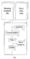
- Fig. 1 illustrates a block scheme of an embodiment of the digital front-end circuit according to the invention.
- Fig. 2 represents an embodiment of the synchronisation and sensing engine comprised in the digital front-end circuit.
- Fig. 3 illustrates the interaction between correlator and processor.
- Fig. 4 illustrates an embodiment of a digital front-end structure comprising a digital front-end circuit as in Fig.1 and 2 , and a number of tiles with only 'sync' functionality.
- the present invention discloses in a first aspect a digital front-end circuit capable of receiving and sensing data encoded according to one of a variety of possible wireless communication standards in a power efficient way.
- the digital front-end circuit of the invention constitutes an interface between the analogue frontend and the baseband (front-end data and control interfaces).
- independent units can be foreseen corresponding to the different antenna paths. These units are also referred to as tiles.
- Each unit can be configured and used independently or in a collaborative way (e.g., for multi-antenna transmission or reception). In particular, for the receive path, an important function is to enable very low power operation of the software defined radio platform through a gradual wakeup of the platform.
- the digital front-end circuit is arranged for performing the signal acquisition and coarse time synchronisation on incoming bursts for the different standards in scope.
- WLAN and LTE are considered as main standards for driving the specifications of the digital front-end circuit according to this invention.
- the proposed solution allows reliable synchronisation on various standards (e.g., WLAN, LTE) and supports spectrum sensing (e.g., WLAN, LTE, DVB-T).
- WLAN, LTE, DVB-T spectrum sensing
- the circuit of the invention is equipped for performing flexible resampling and band selection.
- An interpolator-based approach is envisaged, leading to very flexible rate-support for both integer and fractional rate conversion.
- the digital front-end circuit is capable of performing spectrum sensing to improve coexistence and handover and allow the use of white spaces (i.e. unused spectrum). Specifically, support is added for :
- Fig.1 represents a high-level overview of a circuit architecture according to an embodiment of this invention. Following the datapath from input to host interface the circuit (100) contains the following blocks :
- the AGRAC AGc and Resource Activity Controller (20) can be implemented as a power-optimized microcontroller core that takes care of AGC (Automatic Gain Control) and that controls the activation of other parts of the DIFFS.
- This block is basically the main controller of digital front-end circuit (100) and runs at the incoming sample speed.
- the AGRAC controller is always 'listening' for incoming signal power, while all the other modules are 'sleeping'. If an incoming data packet is detected the other modules are started as required.
- the filtering means (1) comprises a flexible branch (3) with programmable features and a second branch (2) which is strongly power-optimized and (consequently) much less flexible or even fixed and limited in functionality.
- the flexible filter branch supports band selection and resampling and allows for reception and sensing of any subband of the received signal band.
- the flexible filter chain allows coupling advanced receiver front-ends.
- the second filter branch can be used for reception and sensing of a band with center frequency and bandwidth as supported by the reconfigurable analogue front-end.
- the filtering means allows for simultaneous sensing/reception of a wide-band and a narrow-band, i.e., using the fixed and flexible filter branches in parallel.
- the fixed downsample and filter branch (2) contains power-optimized fixed filters/downsamplers that allow low-pass filtering and downsampling, e.g. by factor 2 or 4.
- the fixed filter branch is preferably used in combination with a reconfigurable analogue front-end to allow low-power reception of the supported standards.
- the requirements for those filters depend on the standard to be implemented.
- the adjacent channel suppression can be set to 50 dB. Suppression of the 3 rd adjacent channel is taken care of by the analogue anti-aliasing filters before the ADC in the reconfigurable analogue front-end.
- the flexible filter branch (3) allows reception and processing (band selection) of very wideband signals, as generated e.g. by a bandpass sigma/delta ADC. Also, the functionality of this block enables various sensing strategies to be implemented. Additionally, this filter branch enables coupling the digital front-end to frontends that provide oversampling rates that are not 2 or 4.
- the flexible filter branch is equipped with a resampler enabling non-integer downsampling of the received samples.
- This resampler can e.g. be a Langrange type resampler.
- the flexible filter branch comprises a mixer, a CIC (cascaded integrator-comb) filter, a finite impulse response (FIR) filter and resampler.
- the filters are programmable to provide maximum flexibility.
- the synchronisation and sensing engine is a circuit (4) for performing coarse time synchronisation and advanced spectrum sensing algorithms on the received data.
- the circuit comprises a correlator core (5) to correlate data of the serial stream output by the filter section (1).
- the correlator core offloads the relatively simple, but computationally complex, correlation operations from the processing means (8).
- the output data of the correlator is fed to a vectoriser (7) that transforms the data into vector data.
- power measurement functionality can be provided.
- the correlator can operate in several modes. Auto- or crosscorrelation operations can be applied. In one mode it just acts as a pass-through. In this case the received data are directly applied to the vectorisation means. Additionally the resampler can calculate the power of the received samples.
- processor (8) which can e.g. be a SIMD (Single Instruction Multiple Data) processor.
- the processor also contains a scalar cluster (6) used for control/branch instructions and a vector cluster (10) (in Fig.2 a 32-slot vector cluster) for number crunching.
- the vector cluster is fed with the vectorised data from the vectorisation means.
- the scalar slot (6) supports instructions required to take decisions based on the results of the SIMD. This includes branch instructions (goto, call, return, bneg, bnz), arithmetic instructions (add, sub,%), logic instructions (and, or, xor,%) and instructions to extract results from the vector slot (rgrep, rmax,). No additional data memory is provided for the scalar slot, as no data-intensive algorithms are mapped to this slot. To cover cases where lookup tables would need to be implemented, a special instruction is added to the instruction set that allows mapping lookup tables to functions in program memory (return with immediate value in specific register).
- the vector slot (10) supports all standard arithmetic operations on complex operands (add, sub, mul), logic operations (and, or, xor,%), possibly some masking-specific instructions and finally instructions required to interface with the hardware accelerator cores. Furthermore, the SIMD datapath contains logic for saturation, to avoid problems with overflow. This slot has a limited (e.g. 8) number of vector registers (limited, because they are very costly for the hardware implementation) and some data memory for storing intermediate results, FFT windows and vector masks.
- additional accelerator cores can be provided : a full FFT core (30) and a vector rotator (31).
- An architecture with parallel accelerator cores and a vector processor is advantageous because it enables both synchronization and sensing to be mapped on a solution that reuses the common logic for both synchronisation and sensing.
- the vector slot allows clocking the processor at the incoming sample speed. This way, using a PLL and a higher clock frequency (important for power consumption) is avoided.
- a handshake mechanism is available between the accelerators and the processor. However, it is in software which enables flexible synchronization between the accelerators and the processor. The state of each of the different components (accelerator and processor) is maintained separately by each of these components to enable an asynchronous behaviour as well.
- the FFT accelerator core enables the synchronisation and sensing engine to perform spectral analysis of the input samples.
- the base size of the FFT unit is 128 samples. Both smaller and bigger FFT sizes can be supported. Bigger FFT sizes are implemented through the decimation in time algorithm. This means there is a limit to the FFT size that can be run in real time. Smaller FFT sizes supported by this accelerator core are 16 and 64 samples.
- Some sensing algorithms require operations implementing rotations of vectors. This functionality is mapped on a vector rotation accelerator, which accepts two vectors and supports full-flexible shift/rotations on that data.
- Input samples are fed into the auto/cross correlation unit. They can originate from either of the outputs of the various filter branches present in the digital front-end circuit. This auto/cross correlation unit produces one new complex output sample every clock cycle. These samples are parallelized into a vector of 32 complex samples.
- the SIMD is notified when a new input vector is available. The SIMD supports the usual arithmetic operations on the input samples (add, subtract, multiply, thresholding) and prepares the data for the FFT accelerator core. This includes applying a window to the input samples of the FFT. Once the FFT result is available, it is fed back into the SIMD, where it can be processed (threshold, combination of results for bigger FFT sizes). When processing is done, the sync/sense engine will communicate the result through the host control interface. Specific instructions for the SIMD slot may be added.
- the processor core can put itself to sleep when the computation on the incoming data is done and when new data has not arrived yet. This is shown in Fig.3 .
- stall_request is asserted and the processor will be stalled until new data is available from the correlator.
- various optimizations have been applied to the data path of the processor.
- the selected algorithms for sensing advanced wireless standards typically contain arithmetical operations applied to the received signal power, or on the signal power in certain frequency bins of the received signal.
- the sync/sense engine is built as a SIMD with a complex data path. This SIMD has been constrained to 32 complex 12-bit slots because of the implications of the data path width on chip area and power consumption.
- the digital front-end circuit of the invention comprises one or more receive buffers (22).
- the receive buffers are implemented as asynchronous FIFOs. They both buffer the data before it is sent over the host data interface and take care of the clock domain conversion between the front-end clock and the host clock.
- the received data are applied to a circuit for compensating for impairments that the received data may have undergone.
- These compensation means (21) are provided before the received data enter the filter block.
- Impairments that can be compensated for comprise a DC offset, I/Q imbalance, ...
- An estimation of the DC offset can be performed in the controller block.
- the I/Q imbalance has to be programmed. Compensating the I/Q imbalance is required for proper functioning of the sensing algorithms.
- the digital front-end circuit is implemented as a stand-alone chip with a set of suitable interfaces. External interfaces are advantageously provided for example for a front-end interface and a host interface.
- the front-end interface comprises a clock input, a data receive interface (I/Q inputs) and a front-end control interface (for passing AGC settings).
- the front-end interface is clocked at the clock provided by the front-end.
- the host interface is somewhat more complex, as it contains the combination of a data interface, a control interface and various single-bit control signals required for low-latency interaction with the host system.
- the data interface is a straightforward FIFO interface.
- the control interface is a data/address bus, and is used for programming the various program memories of the core of the digital front-end circuit of this invention, for setting working parameters of specific subblocks of the digital front-end circuit (e.g. filters, AGC settings), and for communication of the results of computations performed by the sync/sense engine of the digital front-end circuit.
- the digital front-end circuit as described above is in an advantageous embodiment of the invention part of a digital front-end structure that comprises at least one further digital front-end circuit. This is illustrated in Fig.4 .
- the one or more further digital front-end circuits are independent units (so called 'tiles') corresponding to the different antenna paths.
- the at least one further digital front-end circuit comprises further filtering means (41) having a third filter branch for filtering the received data either in the first frequency band (used in the digital front-end circuit as previously described), in which case there is multiple input multiple output (MIMO) reception, or in a third frequency band different from said first frequency band, in which case a signal according to another standard can be handled.
- MIMO multiple input multiple output
- the further digital front-end circuit also contains a further circuit (42) for performing synchronisation and spectrum sensing, whereby the further circuit is in connection with the output of the further filtering means, said circuit comprising further correlator means for correlating data output by the further filtering means and further processing means. Also a further controller block (43) for controlling the further filtering means and the further circuit for performing synchronisation and spectrum sensing is provided.
- the further circuit is hence of less complexity. This may be due to the presence of only one filter branch, similar to the first filter branch in the filtering means of the digital front-end circuit as earlier described. Also the further correlator means and/or the further processor means can be reduced in complexity as compared to their counterparts in the front-end circuit of the first tile.
- the further front-end circuit is arranged for performing synchronisation only. This results in a digital front-end structure wherein only one tile performs both sensing and synchronisation and wherein one or more other tiles are provided for performing synchronisation only. Due to the separate filter branches it is possible to handle several frequency bands simultaneously. In the embodiment shown in Fig.4 also compensation means (44) and a receive buffer (45) are shown.
- the further filtering means comprises a fourth filter branch in parallel with said third filter branch and being programmable, so that also the sensing functionality is provided in the further tile.
- the fourth filter branch can filter a selected fourth frequency band for sensing.
- the digital front-end circuit of this invention offers various benefits. It allows power-efficient synchronization and reception of multiple wireless standards. It supports multiple reconfigurable analogue front-end types and advanced sensing algorithms to be able to take advantage of unused spectrum. Further it takes advantage of combined sensing and reception to improve the performance and power-consumption and to support handover.
- the circuit is also built on a future-proof architecture that can support a wide variety of standards (WLAN, LTE, DVB, ). The support comes from a double filter data path, one fixed and low power for reception, one flexible for sensing. Both filter branches feed data into a single sync/sense processor that can perform sync and sensing concurrently.
- Various power savings are embedded in the architecture, both in the chip top level, as in the processor itself.
- top, bottom, over, under, and the like are introduced for descriptive purposes and not necessarily to denote relative positions. It is to be understood that the terms so used are interchangeable under appropriate circumstances and embodiments of the invention are capable of operating according to the present invention in other sequences, or in orientations different from the one(s) described or illustrated above.
Landscapes
- Engineering & Computer Science (AREA)
- Computer Networks & Wireless Communication (AREA)
- Signal Processing (AREA)
- Mobile Radio Communication Systems (AREA)
- Digital Transmission Methods That Use Modulated Carrier Waves (AREA)
- Circuits Of Receivers In General (AREA)
Claims (13)
- Un circuit numérique frontal comprenant :- un moyen de filtrage (1) destiné au filtrage de données reçues, ledit moyen de filtrage comprenant une première branche de filtre (2) destinée au filtrage desdites données reçues dans une première bande de fréquence et une deuxième branche de filtre (3) destinée au filtrage desdites données reçues dans une deuxième bande de fréquence sélectionnée, ladite deuxième bande de fréquence étant différente de ladite première bande de fréquence, ladite deuxième branche de filtre étant parallèle à ladite première branche de filtre, étant programmable et comprenant un moyen de rééchantillonnage destiné au rééchantillonnage desdites données reçues,- un circuit (4) destiné à exécuter une synchronisation et une détection de spectre sur lesdites données reçues, ledit circuit étant en connexion avec la sortie dudit moyen de filtrage (1), ledit circuit (4) comprenanto un moyen de corrélation (5) destiné à corréler une sortie de données par ledit moyen de filtrage,o un moyen (7) de vectorisation de ladite sortie de données par ledit moyen de corrélation ou une autre sortie de données par ledit moyen de filtrage,o un moyen de traitement (8) raccordé audit moyen de vectorisation de données, ledit moyen de traitement comprenant une partie scalaire (6) et une partie vectorielle (10), ladite partie scalaire étant agencée de façon à échanger des instructions de commande avec ledit moyen (7) de vectorisation de données et ladite partie vectorielle, ladite partie vectorielle (10) étant agencée de façon à traiter lesdites données vectorisées, ledit moyen de traitement étant agencé en outre de façon à détecter une présence de signal dans ladite deuxième bande de fréquence sélectionnée,- un bloc de système de commande (20) destiné à commander ledit moyen de filtrage (1 ) et ledit circuit (4) de façon à exécuter une synchronisation et une détection de spectre.
- Un circuit numérique frontal selon la Revendication 1, comprenant un moyen accélérateur de rotation (31) pour une détection améliorée.
- Un circuit numérique frontal selon la Revendication 1 ou 2, comprenant en outre un accélérateur FFT destiné à détecter une présence de signal.
- Un circuit numérique frontal selon l'une quelconque des Revendications 1 à 3, comprenant en outre un moyen de compensation (21) destiné à compenser des données reçues détériorées.
- Un circuit numérique frontal selon la Revendication 4, où ledit moyen de compensation est agencé de façon à compenser un décalage DC et/ou un déséquilibre I/Q.
- Un circuit numérique frontal selon l'une quelconque des Revendications 1 à 5, comprenant en outre une mémoire tampon de réception (22).
- Un circuit numérique frontal selon l'une quelconque des Revendications précédentes, où ledit moyen de traitement est muni d'une horloge agencée de façon à fonctionner à la vitesse desdites données reçues.
- Un circuit numérique frontal selon l'une quelconque des Revendications précédentes, où ledit moyen de traitement comprend un moyen de détection destiné à détecter ladite présence de signal dans ladite deuxième bande de fréquence sélectionnée.
- Une structure numérique frontale comprenant un circuit numérique frontal selon l'une quelconque des Revendications précédentes et au moins un autre circuit numérique frontal, ledit au moins un autre circuit numérique frontal comprenant- un autre moyen de filtrage (41) comprenant une troisième branche de filtre destinée au filtrage desdites données reçues dans ladite première bande de fréquence ou dans une troisième bande de fréquence différente de ladite première bande de fréquence,- un autre circuit (42) destiné à exécuter une synchronisation et une détection de spectre, ledit autre circuit étant en connexion avec la sortie dudit autre moyen de filtrage, ledit autre circuit (42) comprenanto un autre moyen de corrélation destiné à corréler une sortie de données par ledit autre moyen de filtrage,o un autre moyen de traitement,- un autre bloc de système de commande (43) destiné à commander ledit autre moyen de filtrage et ledit autre circuit de façon à exécuter une synchronisation et une détection de spectre.
- Une structure numérique frontale selon la Revendication 9, grâce à laquelle ledit autre moyen de filtrage comprend une quatrième branche de filtre programmable parallèle à ladite troisième branche de filtre.
- Un récepteur numérique comprenant un circuit numérique frontal ou une structure numérique frontale selon l'une quelconque des Revendications précédentes.
- Un récepteur numérique selon la Revendication 11, comprenant en outre un circuit frontal analogique reconfigurable.
- Un procédé d'exécution simultanée d'une synchronisation et d'une détection de spectre sur des données reçues dans un circuit numérique frontal, comprenant les opérations suivantes :- le filtrage desdites données reçues dans une première bande de fréquence par l'intermédiaire d'une première branche de filtre et le filtrage desdites données reçues dans une deuxième bande de fréquence sélectionnée par l'intermédiaire d'une deuxième branche de filtre parallèle à ladite première branche de filtre, ladite deuxième bande de fréquence étant différente de ladite première bande de fréquence,- l'exécution d'une opération de synchronisation sur lesdites données reçues filtrées dans ladite première bande de fréquence avec un circuit destiné à exécuter une synchronisation et une détection de spectre contenu dans ledit circuit numérique frontal,- l'envoi de données synchronisées à une sortie de données dudit circuit numérique frontal,- l'exécution d'une opération de détection sur lesdites données reçues filtrées dans ladite deuxième bande de fréquence sélectionnée avec ledit circuit destiné à exécuter une synchronisation et une détection de spectre contenu dans ledit circuit numérique frontal,- la production d'informations relatives aux données détectées.
Priority Applications (4)
| Application Number | Priority Date | Filing Date | Title |
|---|---|---|---|
| EP20100153967 EP2362550B1 (fr) | 2010-02-18 | 2010-02-18 | Circuit frontal numérique et son procédé d'utilisation |
| PCT/EP2011/051357 WO2011101233A1 (fr) | 2010-02-18 | 2011-02-01 | Circuit numérique frontal et son procédé d'utilisation |
| JP2012553251A JP2013520117A (ja) | 2010-02-18 | 2011-02-01 | デジタルフロントエンド回路及びデジタルフロントエンド回路を使用するための方法 |
| US13/563,243 US8861656B2 (en) | 2010-02-18 | 2012-07-31 | Digital front-end circuit and method for using the same |
Applications Claiming Priority (1)
| Application Number | Priority Date | Filing Date | Title |
|---|---|---|---|
| EP20100153967 EP2362550B1 (fr) | 2010-02-18 | 2010-02-18 | Circuit frontal numérique et son procédé d'utilisation |
Publications (2)
| Publication Number | Publication Date |
|---|---|
| EP2362550A1 EP2362550A1 (fr) | 2011-08-31 |
| EP2362550B1 true EP2362550B1 (fr) | 2012-08-29 |
Family
ID=42110140
Family Applications (1)
| Application Number | Title | Priority Date | Filing Date |
|---|---|---|---|
| EP20100153967 Not-in-force EP2362550B1 (fr) | 2010-02-18 | 2010-02-18 | Circuit frontal numérique et son procédé d'utilisation |
Country Status (4)
| Country | Link |
|---|---|
| US (1) | US8861656B2 (fr) |
| EP (1) | EP2362550B1 (fr) |
| JP (1) | JP2013520117A (fr) |
| WO (1) | WO2011101233A1 (fr) |
Families Citing this family (7)
| Publication number | Priority date | Publication date | Assignee | Title |
|---|---|---|---|---|
| US9363068B2 (en) | 2010-08-03 | 2016-06-07 | Intel Corporation | Vector processor having instruction set with sliding window non-linear convolutional function |
| RU2012102842A (ru) | 2012-01-27 | 2013-08-10 | ЭлЭсАй Корпорейшн | Инкрементное обнаружение преамбулы |
| KR20140084294A (ko) * | 2011-10-27 | 2014-07-04 | 엘에스아이 코포레이션 | 복소 지수 비선형 함수와 함께 명령어를 갖는 디지털 처리 |
| US9612816B2 (en) * | 2012-04-12 | 2017-04-04 | Industry-University Cooperation Foundation Hanyang University | Method for operating software defined radio application |
| US9088521B2 (en) * | 2013-02-21 | 2015-07-21 | Litepoint Corporation | System and method for testing multiple data packet signal transceivers concurrently |
| US9923595B2 (en) | 2013-04-17 | 2018-03-20 | Intel Corporation | Digital predistortion for dual-band power amplifiers |
| EP2813344B1 (fr) * | 2013-06-10 | 2016-11-16 | Discma AG | Appareil et procédé de fabrication des récipients |
Family Cites Families (15)
| Publication number | Priority date | Publication date | Assignee | Title |
|---|---|---|---|---|
| US7346134B2 (en) * | 2001-05-15 | 2008-03-18 | Finesse Wireless, Inc. | Radio receiver |
| WO2005122414A1 (fr) * | 2004-06-14 | 2005-12-22 | Matsushita Electric Industrial Co., Ltd. | Dispositif de communication radio |
| DE102004047683B4 (de) * | 2004-09-30 | 2007-05-10 | Advanced Micro Devices, Inc., Sunnyvale | Niedrig-IF-Mehrfachmodus-Sender-Front-End und entsprechendes Verfahren |
| WO2007132016A1 (fr) | 2006-05-16 | 2007-11-22 | Interuniversitair Microelektronica Centrum (Imec) | Récepteur numérique permettant l'utilisation de radio logicielle |
| US8687563B2 (en) * | 2007-01-09 | 2014-04-01 | Stmicroelectronics, Inc. | Simultaneous sensing and data transmission |
| US8437314B2 (en) * | 2007-02-22 | 2013-05-07 | Stmicroelectronics, Inc. | Radio frequency architecture for spectrum access networks |
| JP2010522455A (ja) * | 2007-03-19 | 2010-07-01 | コーニンクレッカ フィリップス エレクトロニクス エヌ ヴィ | 既存の信号のfftに基づくパイロット検知 |
| JP2008252490A (ja) * | 2007-03-30 | 2008-10-16 | Toyota Infotechnology Center Co Ltd | 無線機 |
| US8582694B2 (en) * | 2007-04-30 | 2013-11-12 | Scott R. Velazquez | Adaptive digital receiver |
| US20080279290A1 (en) * | 2007-05-09 | 2008-11-13 | At&T Knowledge Ventures, Lp | Technique for Operating a Communication System at a Higher Spectral Utilization for Wireless Broadband Applications |
| US8036240B2 (en) * | 2007-12-14 | 2011-10-11 | Microsoft Corporation | Software defined cognitive radio |
| US8081722B1 (en) * | 2008-04-04 | 2011-12-20 | Harris Corporation | Communications system and device using simultaneous wideband and in-band narrowband operation and related method |
| JP2010056978A (ja) * | 2008-08-29 | 2010-03-11 | Renesas Technology Corp | 半導体集積回路およびその動作方法 |
| US8299947B2 (en) * | 2009-06-26 | 2012-10-30 | Syntropy Systems, Llc | Sampling/quantization converters |
| JP5370889B2 (ja) * | 2009-07-24 | 2013-12-18 | 独立行政法人情報通信研究機構 | コグニティブ無線通信用スペクトラムセンサー及びコグニティブ無線通信方法 |
-
2010
- 2010-02-18 EP EP20100153967 patent/EP2362550B1/fr not_active Not-in-force
-
2011
- 2011-02-01 JP JP2012553251A patent/JP2013520117A/ja active Pending
- 2011-02-01 WO PCT/EP2011/051357 patent/WO2011101233A1/fr active Application Filing
-
2012
- 2012-07-31 US US13/563,243 patent/US8861656B2/en not_active Expired - Fee Related
Also Published As
| Publication number | Publication date |
|---|---|
| US20130022157A1 (en) | 2013-01-24 |
| US8861656B2 (en) | 2014-10-14 |
| WO2011101233A1 (fr) | 2011-08-25 |
| EP2362550A1 (fr) | 2011-08-31 |
| JP2013520117A (ja) | 2013-05-30 |
Similar Documents
| Publication | Publication Date | Title |
|---|---|---|
| US8861656B2 (en) | Digital front-end circuit and method for using the same | |
| JP4276677B2 (ja) | 無線通信装置 | |
| US8718559B2 (en) | Method, apparatus and computer program for sensing spectrum in a cognitive radio environment | |
| US20090274202A1 (en) | System partitioning for multi-mobile devices | |
| CN103781085A (zh) | 一种多频段tetra数字集群检测方法和装置 | |
| CN101174840B (zh) | 多组频带的可程控直接射频数字化接收器及其方法 | |
| US8498602B2 (en) | Architecture of future open wireless architecture (OWA) radio system | |
| CN101116272A (zh) | 通信装置 | |
| EP2754246B1 (fr) | Systèmes et procédés de démodulation et de modulation sur des radios définies par logiciel | |
| EP3195645A1 (fr) | Procédé et agencement pour communication multibande | |
| US9497799B2 (en) | Method for controlling RF signal processing components and communications apparatus utilizing the same | |
| Dejonghe et al. | Versatile spectrum sensing on mobile devices? | |
| Tachwali et al. | Adaptability and configurability in cognitive radio design on small form factor software radio platform | |
| Lu et al. | A single FPGA embedded framework for secondary user in cognitive network | |
| Kocks et al. | A cognitive radio realization based on a petri net approach | |
| US20170177542A1 (en) | Operating a VLIW Processor in a Wireless Sensor Device | |
| CN109600148B (zh) | 多模扫频仪及扫频控制方法 | |
| Rakhshanfar et al. | Implementation of software radio based on PC and FPGA | |
| EP1914900A1 (fr) | Récepteur numérique pour implémentation radio définie via logiciel | |
| Chiumento et al. | Diffs: a low power, multi-mode, multi-standard flexible digital front-end for sensing in future cognitive radios | |
| Immonen et al. | A reconfigurable multi-standard radio platform | |
| Diaz et al. | Nex generation digital front-end for multi-standard concurrent reception | |
| WO2023121489A1 (fr) | Accès à la commande et à la mémoire à l'aide d'une diffusion audio en continu | |
| CA2847969C (fr) | Systemes et procedes de demodulation et de modulation sur des radios definies par logiciel | |
| KR100759454B1 (ko) | 무선 랜에서 다중 동일 네트워크 인터페이스 시스템 |
Legal Events
| Date | Code | Title | Description |
|---|---|---|---|
| PUAI | Public reference made under article 153(3) epc to a published international application that has entered the european phase |
Free format text: ORIGINAL CODE: 0009012 |
|
| AK | Designated contracting states |
Kind code of ref document: A1 Designated state(s): AT BE BG CH CY CZ DE DK EE ES FI FR GB GR HR HU IE IS IT LI LT LU LV MC MK MT NL NO PL PT RO SE SI SK SM TR |
|
| 17P | Request for examination filed |
Effective date: 20120228 |
|
| GRAP | Despatch of communication of intention to grant a patent |
Free format text: ORIGINAL CODE: EPIDOSNIGR1 |
|
| GRAS | Grant fee paid |
Free format text: ORIGINAL CODE: EPIDOSNIGR3 |
|
| GRAA | (expected) grant |
Free format text: ORIGINAL CODE: 0009210 |
|
| AK | Designated contracting states |
Kind code of ref document: B1 Designated state(s): AT BE BG CH CY CZ DE DK EE ES FI FR GB GR HR HU IE IS IT LI LT LU LV MC MK MT NL NO PL PT RO SE SI SK SM TR |
|
| REG | Reference to a national code |
Ref country code: GB Ref legal event code: FG4D |
|
| REG | Reference to a national code |
Ref country code: CH Ref legal event code: EP |
|
| REG | Reference to a national code |
Ref country code: AT Ref legal event code: REF Ref document number: 573517 Country of ref document: AT Kind code of ref document: T Effective date: 20120915 |
|
| REG | Reference to a national code |
Ref country code: IE Ref legal event code: FG4D |
|
| REG | Reference to a national code |
Ref country code: DE Ref legal event code: R096 Ref document number: 602010002579 Country of ref document: DE Effective date: 20121025 |
|
| REG | Reference to a national code |
Ref country code: AT Ref legal event code: MK05 Ref document number: 573517 Country of ref document: AT Kind code of ref document: T Effective date: 20120829 |
|
| REG | Reference to a national code |
Ref country code: NL Ref legal event code: VDEP Effective date: 20120829 |
|
| REG | Reference to a national code |
Ref country code: LT Ref legal event code: MG4D Effective date: 20120829 |
|
| PG25 | Lapsed in a contracting state [announced via postgrant information from national office to epo] |
Ref country code: HR Free format text: LAPSE BECAUSE OF FAILURE TO SUBMIT A TRANSLATION OF THE DESCRIPTION OR TO PAY THE FEE WITHIN THE PRESCRIBED TIME-LIMIT Effective date: 20120829 Ref country code: LT Free format text: LAPSE BECAUSE OF FAILURE TO SUBMIT A TRANSLATION OF THE DESCRIPTION OR TO PAY THE FEE WITHIN THE PRESCRIBED TIME-LIMIT Effective date: 20120829 Ref country code: AT Free format text: LAPSE BECAUSE OF FAILURE TO SUBMIT A TRANSLATION OF THE DESCRIPTION OR TO PAY THE FEE WITHIN THE PRESCRIBED TIME-LIMIT Effective date: 20120829 Ref country code: IS Free format text: LAPSE BECAUSE OF FAILURE TO SUBMIT A TRANSLATION OF THE DESCRIPTION OR TO PAY THE FEE WITHIN THE PRESCRIBED TIME-LIMIT Effective date: 20121229 Ref country code: NO Free format text: LAPSE BECAUSE OF FAILURE TO SUBMIT A TRANSLATION OF THE DESCRIPTION OR TO PAY THE FEE WITHIN THE PRESCRIBED TIME-LIMIT Effective date: 20121129 Ref country code: FI Free format text: LAPSE BECAUSE OF FAILURE TO SUBMIT A TRANSLATION OF THE DESCRIPTION OR TO PAY THE FEE WITHIN THE PRESCRIBED TIME-LIMIT Effective date: 20120829 |
|
| PG25 | Lapsed in a contracting state [announced via postgrant information from national office to epo] |
Ref country code: GR Free format text: LAPSE BECAUSE OF FAILURE TO SUBMIT A TRANSLATION OF THE DESCRIPTION OR TO PAY THE FEE WITHIN THE PRESCRIBED TIME-LIMIT Effective date: 20121130 Ref country code: SE Free format text: LAPSE BECAUSE OF FAILURE TO SUBMIT A TRANSLATION OF THE DESCRIPTION OR TO PAY THE FEE WITHIN THE PRESCRIBED TIME-LIMIT Effective date: 20120829 Ref country code: BE Free format text: LAPSE BECAUSE OF FAILURE TO SUBMIT A TRANSLATION OF THE DESCRIPTION OR TO PAY THE FEE WITHIN THE PRESCRIBED TIME-LIMIT Effective date: 20120829 Ref country code: PT Free format text: LAPSE BECAUSE OF FAILURE TO SUBMIT A TRANSLATION OF THE DESCRIPTION OR TO PAY THE FEE WITHIN THE PRESCRIBED TIME-LIMIT Effective date: 20121231 Ref country code: LV Free format text: LAPSE BECAUSE OF FAILURE TO SUBMIT A TRANSLATION OF THE DESCRIPTION OR TO PAY THE FEE WITHIN THE PRESCRIBED TIME-LIMIT Effective date: 20120829 Ref country code: SI Free format text: LAPSE BECAUSE OF FAILURE TO SUBMIT A TRANSLATION OF THE DESCRIPTION OR TO PAY THE FEE WITHIN THE PRESCRIBED TIME-LIMIT Effective date: 20120829 |
|
| PG25 | Lapsed in a contracting state [announced via postgrant information from national office to epo] |
Ref country code: CZ Free format text: LAPSE BECAUSE OF FAILURE TO SUBMIT A TRANSLATION OF THE DESCRIPTION OR TO PAY THE FEE WITHIN THE PRESCRIBED TIME-LIMIT Effective date: 20120829 Ref country code: NL Free format text: LAPSE BECAUSE OF FAILURE TO SUBMIT A TRANSLATION OF THE DESCRIPTION OR TO PAY THE FEE WITHIN THE PRESCRIBED TIME-LIMIT Effective date: 20120829 Ref country code: RO Free format text: LAPSE BECAUSE OF FAILURE TO SUBMIT A TRANSLATION OF THE DESCRIPTION OR TO PAY THE FEE WITHIN THE PRESCRIBED TIME-LIMIT Effective date: 20120829 Ref country code: EE Free format text: LAPSE BECAUSE OF FAILURE TO SUBMIT A TRANSLATION OF THE DESCRIPTION OR TO PAY THE FEE WITHIN THE PRESCRIBED TIME-LIMIT Effective date: 20120829 Ref country code: DK Free format text: LAPSE BECAUSE OF FAILURE TO SUBMIT A TRANSLATION OF THE DESCRIPTION OR TO PAY THE FEE WITHIN THE PRESCRIBED TIME-LIMIT Effective date: 20120829 |
|
| PG25 | Lapsed in a contracting state [announced via postgrant information from national office to epo] |
Ref country code: SK Free format text: LAPSE BECAUSE OF FAILURE TO SUBMIT A TRANSLATION OF THE DESCRIPTION OR TO PAY THE FEE WITHIN THE PRESCRIBED TIME-LIMIT Effective date: 20120829 Ref country code: PL Free format text: LAPSE BECAUSE OF FAILURE TO SUBMIT A TRANSLATION OF THE DESCRIPTION OR TO PAY THE FEE WITHIN THE PRESCRIBED TIME-LIMIT Effective date: 20120829 Ref country code: IT Free format text: LAPSE BECAUSE OF FAILURE TO SUBMIT A TRANSLATION OF THE DESCRIPTION OR TO PAY THE FEE WITHIN THE PRESCRIBED TIME-LIMIT Effective date: 20120829 |
|
| PLBE | No opposition filed within time limit |
Free format text: ORIGINAL CODE: 0009261 |
|
| STAA | Information on the status of an ep patent application or granted ep patent |
Free format text: STATUS: NO OPPOSITION FILED WITHIN TIME LIMIT |
|
| PG25 | Lapsed in a contracting state [announced via postgrant information from national office to epo] |
Ref country code: BG Free format text: LAPSE BECAUSE OF FAILURE TO SUBMIT A TRANSLATION OF THE DESCRIPTION OR TO PAY THE FEE WITHIN THE PRESCRIBED TIME-LIMIT Effective date: 20121129 |
|
| 26N | No opposition filed |
Effective date: 20130530 |
|
| REG | Reference to a national code |
Ref country code: DE Ref legal event code: R097 Ref document number: 602010002579 Country of ref document: DE Effective date: 20130530 |
|
| PG25 | Lapsed in a contracting state [announced via postgrant information from national office to epo] |
Ref country code: MC Free format text: LAPSE BECAUSE OF NON-PAYMENT OF DUE FEES Effective date: 20130228 |
|
| PG25 | Lapsed in a contracting state [announced via postgrant information from national office to epo] |
Ref country code: ES Free format text: LAPSE BECAUSE OF FAILURE TO SUBMIT A TRANSLATION OF THE DESCRIPTION OR TO PAY THE FEE WITHIN THE PRESCRIBED TIME-LIMIT Effective date: 20121210 |
|
| PG25 | Lapsed in a contracting state [announced via postgrant information from national office to epo] |
Ref country code: CY Free format text: LAPSE BECAUSE OF FAILURE TO SUBMIT A TRANSLATION OF THE DESCRIPTION OR TO PAY THE FEE WITHIN THE PRESCRIBED TIME-LIMIT Effective date: 20120829 |
|
| REG | Reference to a national code |
Ref country code: IE Ref legal event code: MM4A |
|
| PG25 | Lapsed in a contracting state [announced via postgrant information from national office to epo] |
Ref country code: IE Free format text: LAPSE BECAUSE OF NON-PAYMENT OF DUE FEES Effective date: 20130218 |
|
| PG25 | Lapsed in a contracting state [announced via postgrant information from national office to epo] |
Ref country code: MT Free format text: LAPSE BECAUSE OF FAILURE TO SUBMIT A TRANSLATION OF THE DESCRIPTION OR TO PAY THE FEE WITHIN THE PRESCRIBED TIME-LIMIT Effective date: 20120829 |
|
| REG | Reference to a national code |
Ref country code: CH Ref legal event code: PL |
|
| PG25 | Lapsed in a contracting state [announced via postgrant information from national office to epo] |
Ref country code: LI Free format text: LAPSE BECAUSE OF NON-PAYMENT OF DUE FEES Effective date: 20140228 Ref country code: CH Free format text: LAPSE BECAUSE OF NON-PAYMENT OF DUE FEES Effective date: 20140228 |
|
| PG25 | Lapsed in a contracting state [announced via postgrant information from national office to epo] |
Ref country code: SM Free format text: LAPSE BECAUSE OF FAILURE TO SUBMIT A TRANSLATION OF THE DESCRIPTION OR TO PAY THE FEE WITHIN THE PRESCRIBED TIME-LIMIT Effective date: 20120829 |
|
| PG25 | Lapsed in a contracting state [announced via postgrant information from national office to epo] |
Ref country code: TR Free format text: LAPSE BECAUSE OF FAILURE TO SUBMIT A TRANSLATION OF THE DESCRIPTION OR TO PAY THE FEE WITHIN THE PRESCRIBED TIME-LIMIT Effective date: 20120829 |
|
| PG25 | Lapsed in a contracting state [announced via postgrant information from national office to epo] |
Ref country code: LU Free format text: LAPSE BECAUSE OF NON-PAYMENT OF DUE FEES Effective date: 20130218 Ref country code: HU Free format text: LAPSE BECAUSE OF FAILURE TO SUBMIT A TRANSLATION OF THE DESCRIPTION OR TO PAY THE FEE WITHIN THE PRESCRIBED TIME-LIMIT; INVALID AB INITIO Effective date: 20100218 Ref country code: MK Free format text: LAPSE BECAUSE OF FAILURE TO SUBMIT A TRANSLATION OF THE DESCRIPTION OR TO PAY THE FEE WITHIN THE PRESCRIBED TIME-LIMIT Effective date: 20120829 |
|
| REG | Reference to a national code |
Ref country code: FR Ref legal event code: PLFP Year of fee payment: 7 |
|
| REG | Reference to a national code |
Ref country code: FR Ref legal event code: PLFP Year of fee payment: 8 |
|
| REG | Reference to a national code |
Ref country code: FR Ref legal event code: PLFP Year of fee payment: 9 |
|
| PGFP | Annual fee paid to national office [announced via postgrant information from national office to epo] |
Ref country code: FR Payment date: 20210120 Year of fee payment: 12 |
|
| PGFP | Annual fee paid to national office [announced via postgrant information from national office to epo] |
Ref country code: GB Payment date: 20210120 Year of fee payment: 12 Ref country code: DE Payment date: 20210120 Year of fee payment: 12 |
|
| REG | Reference to a national code |
Ref country code: DE Ref legal event code: R119 Ref document number: 602010002579 Country of ref document: DE |
|
| GBPC | Gb: european patent ceased through non-payment of renewal fee |
Effective date: 20220218 |
|
| PG25 | Lapsed in a contracting state [announced via postgrant information from national office to epo] |
Ref country code: FR Free format text: LAPSE BECAUSE OF NON-PAYMENT OF DUE FEES Effective date: 20220228 |
|
| PG25 | Lapsed in a contracting state [announced via postgrant information from national office to epo] |
Ref country code: GB Free format text: LAPSE BECAUSE OF NON-PAYMENT OF DUE FEES Effective date: 20220218 Ref country code: DE Free format text: LAPSE BECAUSE OF NON-PAYMENT OF DUE FEES Effective date: 20220901 |