EP2362417A2 - A semiconductor device having a suspended isolating interconnect - Google Patents
A semiconductor device having a suspended isolating interconnect Download PDFInfo
- Publication number
- EP2362417A2 EP2362417A2 EP11004204A EP11004204A EP2362417A2 EP 2362417 A2 EP2362417 A2 EP 2362417A2 EP 11004204 A EP11004204 A EP 11004204A EP 11004204 A EP11004204 A EP 11004204A EP 2362417 A2 EP2362417 A2 EP 2362417A2
- Authority
- EP
- European Patent Office
- Prior art keywords
- wires
- interconnect
- semiconductor device
- wire
- semiconductor die
- Prior art date
- Legal status (The legal status is an assumption and is not a legal conclusion. Google has not performed a legal analysis and makes no representation as to the accuracy of the status listed.)
- Granted
Links
Images

Classifications
-
- H—ELECTRICITY
- H01—ELECTRIC ELEMENTS
- H01F—MAGNETS; INDUCTANCES; TRANSFORMERS; SELECTION OF MATERIALS FOR THEIR MAGNETIC PROPERTIES
- H01F19/00—Fixed transformers or mutual inductances of the signal type
- H01F19/04—Transformers or mutual inductances suitable for handling frequencies considerably beyond the audio range
- H01F19/08—Transformers having magnetic bias, e.g. for handling pulses
-
- H—ELECTRICITY
- H10—SEMICONDUCTOR DEVICES; ELECTRIC SOLID-STATE DEVICES NOT OTHERWISE PROVIDED FOR
- H10W—GENERIC PACKAGES, INTERCONNECTIONS, CONNECTORS OR OTHER CONSTRUCTIONAL DETAILS OF DEVICES COVERED BY CLASS H10
- H10W44/00—Electrical arrangements for controlling or matching impedance
- H10W44/501—Inductive arrangements
-
- H—ELECTRICITY
- H10—SEMICONDUCTOR DEVICES; ELECTRIC SOLID-STATE DEVICES NOT OTHERWISE PROVIDED FOR
- H10W—GENERIC PACKAGES, INTERCONNECTIONS, CONNECTORS OR OTHER CONSTRUCTIONAL DETAILS OF DEVICES COVERED BY CLASS H10
- H10W44/00—Electrical arrangements for controlling or matching impedance
- H10W44/601—Capacitive arrangements
-
- H—ELECTRICITY
- H10—SEMICONDUCTOR DEVICES; ELECTRIC SOLID-STATE DEVICES NOT OTHERWISE PROVIDED FOR
- H10W—GENERIC PACKAGES, INTERCONNECTIONS, CONNECTORS OR OTHER CONSTRUCTIONAL DETAILS OF DEVICES COVERED BY CLASS H10
- H10W70/00—Package substrates; Interposers; Redistribution layers [RDL]
- H10W70/40—Leadframes
- H10W70/464—Additional interconnections in combination with leadframes
- H10W70/465—Bumps or wires
-
- H—ELECTRICITY
- H10—SEMICONDUCTOR DEVICES; ELECTRIC SOLID-STATE DEVICES NOT OTHERWISE PROVIDED FOR
- H10W—GENERIC PACKAGES, INTERCONNECTIONS, CONNECTORS OR OTHER CONSTRUCTIONAL DETAILS OF DEVICES COVERED BY CLASS H10
- H10W72/00—Interconnections or connectors in packages
-
- H—ELECTRICITY
- H10—SEMICONDUCTOR DEVICES; ELECTRIC SOLID-STATE DEVICES NOT OTHERWISE PROVIDED FOR
- H10W—GENERIC PACKAGES, INTERCONNECTIONS, CONNECTORS OR OTHER CONSTRUCTIONAL DETAILS OF DEVICES COVERED BY CLASS H10
- H10W72/00—Interconnections or connectors in packages
- H10W72/90—Bond pads, in general
-
- H—ELECTRICITY
- H10—SEMICONDUCTOR DEVICES; ELECTRIC SOLID-STATE DEVICES NOT OTHERWISE PROVIDED FOR
- H10W—GENERIC PACKAGES, INTERCONNECTIONS, CONNECTORS OR OTHER CONSTRUCTIONAL DETAILS OF DEVICES COVERED BY CLASS H10
- H10W90/00—Package configurations
- H10W90/20—Configurations of stacked chips
- H10W90/293—Configurations of stacked chips characterised by non-galvanic coupling between the chips, e.g. capacitive coupling
-
- H—ELECTRICITY
- H01—ELECTRIC ELEMENTS
- H01F—MAGNETS; INDUCTANCES; TRANSFORMERS; SELECTION OF MATERIALS FOR THEIR MAGNETIC PROPERTIES
- H01F19/00—Fixed transformers or mutual inductances of the signal type
- H01F19/04—Transformers or mutual inductances suitable for handling frequencies considerably beyond the audio range
- H01F19/08—Transformers having magnetic bias, e.g. for handling pulses
- H01F2019/085—Transformer for galvanic isolation
-
- H—ELECTRICITY
- H01—ELECTRIC ELEMENTS
- H01F—MAGNETS; INDUCTANCES; TRANSFORMERS; SELECTION OF MATERIALS FOR THEIR MAGNETIC PROPERTIES
- H01F27/00—Details of transformers or inductances, in general
- H01F27/28—Coils; Windings; Conductive connections
- H01F27/2804—Printed windings
- H01F2027/2814—Printed windings with only part of the coil or of the winding in the printed circuit board, e.g. the remaining coil or winding sections can be made of wires or sheets
-
- H—ELECTRICITY
- H01—ELECTRIC ELEMENTS
- H01F—MAGNETS; INDUCTANCES; TRANSFORMERS; SELECTION OF MATERIALS FOR THEIR MAGNETIC PROPERTIES
- H01F38/00—Adaptations of transformers or inductances for specific applications or functions
- H01F38/14—Inductive couplings
-
- H—ELECTRICITY
- H10—SEMICONDUCTOR DEVICES; ELECTRIC SOLID-STATE DEVICES NOT OTHERWISE PROVIDED FOR
- H10W—GENERIC PACKAGES, INTERCONNECTIONS, CONNECTORS OR OTHER CONSTRUCTIONAL DETAILS OF DEVICES COVERED BY CLASS H10
- H10W44/00—Electrical arrangements for controlling or matching impedance
- H10W44/20—Electrical arrangements for controlling or matching impedance at high-frequency [HF] or radio frequency [RF]
- H10W44/203—Electrical connections
- H10W44/206—Wires
-
- H—ELECTRICITY
- H10—SEMICONDUCTOR DEVICES; ELECTRIC SOLID-STATE DEVICES NOT OTHERWISE PROVIDED FOR
- H10W—GENERIC PACKAGES, INTERCONNECTIONS, CONNECTORS OR OTHER CONSTRUCTIONAL DETAILS OF DEVICES COVERED BY CLASS H10
- H10W70/00—Package substrates; Interposers; Redistribution layers [RDL]
- H10W70/60—Insulating or insulated package substrates; Interposers; Redistribution layers
-
- H—ELECTRICITY
- H10—SEMICONDUCTOR DEVICES; ELECTRIC SOLID-STATE DEVICES NOT OTHERWISE PROVIDED FOR
- H10W—GENERIC PACKAGES, INTERCONNECTIONS, CONNECTORS OR OTHER CONSTRUCTIONAL DETAILS OF DEVICES COVERED BY CLASS H10
- H10W72/00—Interconnections or connectors in packages
- H10W72/071—Connecting or disconnecting
- H10W72/075—Connecting or disconnecting of bond wires
-
- H—ELECTRICITY
- H10—SEMICONDUCTOR DEVICES; ELECTRIC SOLID-STATE DEVICES NOT OTHERWISE PROVIDED FOR
- H10W—GENERIC PACKAGES, INTERCONNECTIONS, CONNECTORS OR OTHER CONSTRUCTIONAL DETAILS OF DEVICES COVERED BY CLASS H10
- H10W72/00—Interconnections or connectors in packages
- H10W72/071—Connecting or disconnecting
- H10W72/075—Connecting or disconnecting of bond wires
- H10W72/07551—Connecting or disconnecting of bond wires characterised by changes in properties of the bond wires during the connecting
- H10W72/07553—Connecting or disconnecting of bond wires characterised by changes in properties of the bond wires during the connecting changes in shapes
-
- H—ELECTRICITY
- H10—SEMICONDUCTOR DEVICES; ELECTRIC SOLID-STATE DEVICES NOT OTHERWISE PROVIDED FOR
- H10W—GENERIC PACKAGES, INTERCONNECTIONS, CONNECTORS OR OTHER CONSTRUCTIONAL DETAILS OF DEVICES COVERED BY CLASS H10
- H10W72/00—Interconnections or connectors in packages
- H10W72/071—Connecting or disconnecting
- H10W72/075—Connecting or disconnecting of bond wires
- H10W72/07551—Connecting or disconnecting of bond wires characterised by changes in properties of the bond wires during the connecting
- H10W72/07554—Connecting or disconnecting of bond wires characterised by changes in properties of the bond wires during the connecting changes in dispositions
-
- H—ELECTRICITY
- H10—SEMICONDUCTOR DEVICES; ELECTRIC SOLID-STATE DEVICES NOT OTHERWISE PROVIDED FOR
- H10W—GENERIC PACKAGES, INTERCONNECTIONS, CONNECTORS OR OTHER CONSTRUCTIONAL DETAILS OF DEVICES COVERED BY CLASS H10
- H10W72/00—Interconnections or connectors in packages
- H10W72/50—Bond wires
- H10W72/531—Shapes of wire connectors
- H10W72/536—Shapes of wire connectors the connected ends being ball-shaped
-
- H—ELECTRICITY
- H10—SEMICONDUCTOR DEVICES; ELECTRIC SOLID-STATE DEVICES NOT OTHERWISE PROVIDED FOR
- H10W—GENERIC PACKAGES, INTERCONNECTIONS, CONNECTORS OR OTHER CONSTRUCTIONAL DETAILS OF DEVICES COVERED BY CLASS H10
- H10W72/00—Interconnections or connectors in packages
- H10W72/50—Bond wires
- H10W72/531—Shapes of wire connectors
- H10W72/5366—Shapes of wire connectors the bond wires having kinks
-
- H—ELECTRICITY
- H10—SEMICONDUCTOR DEVICES; ELECTRIC SOLID-STATE DEVICES NOT OTHERWISE PROVIDED FOR
- H10W—GENERIC PACKAGES, INTERCONNECTIONS, CONNECTORS OR OTHER CONSTRUCTIONAL DETAILS OF DEVICES COVERED BY CLASS H10
- H10W72/00—Interconnections or connectors in packages
- H10W72/50—Bond wires
- H10W72/531—Shapes of wire connectors
- H10W72/537—Multiple bond wires having different shapes
-
- H—ELECTRICITY
- H10—SEMICONDUCTOR DEVICES; ELECTRIC SOLID-STATE DEVICES NOT OTHERWISE PROVIDED FOR
- H10W—GENERIC PACKAGES, INTERCONNECTIONS, CONNECTORS OR OTHER CONSTRUCTIONAL DETAILS OF DEVICES COVERED BY CLASS H10
- H10W72/00—Interconnections or connectors in packages
- H10W72/50—Bond wires
- H10W72/541—Dispositions of bond wires
- H10W72/5434—Dispositions of bond wires the connected ends being on auxiliary connecting means on bond pads, e.g. on other bond wires
-
- H—ELECTRICITY
- H10—SEMICONDUCTOR DEVICES; ELECTRIC SOLID-STATE DEVICES NOT OTHERWISE PROVIDED FOR
- H10W—GENERIC PACKAGES, INTERCONNECTIONS, CONNECTORS OR OTHER CONSTRUCTIONAL DETAILS OF DEVICES COVERED BY CLASS H10
- H10W72/00—Interconnections or connectors in packages
- H10W72/50—Bond wires
- H10W72/541—Dispositions of bond wires
- H10W72/5445—Dispositions of bond wires being orthogonal to a side surface of the chip, e.g. parallel arrangements
-
- H—ELECTRICITY
- H10—SEMICONDUCTOR DEVICES; ELECTRIC SOLID-STATE DEVICES NOT OTHERWISE PROVIDED FOR
- H10W—GENERIC PACKAGES, INTERCONNECTIONS, CONNECTORS OR OTHER CONSTRUCTIONAL DETAILS OF DEVICES COVERED BY CLASS H10
- H10W72/00—Interconnections or connectors in packages
- H10W72/50—Bond wires
- H10W72/541—Dispositions of bond wires
- H10W72/547—Dispositions of multiple bond wires
-
- H—ELECTRICITY
- H10—SEMICONDUCTOR DEVICES; ELECTRIC SOLID-STATE DEVICES NOT OTHERWISE PROVIDED FOR
- H10W—GENERIC PACKAGES, INTERCONNECTIONS, CONNECTORS OR OTHER CONSTRUCTIONAL DETAILS OF DEVICES COVERED BY CLASS H10
- H10W72/00—Interconnections or connectors in packages
- H10W72/50—Bond wires
- H10W72/551—Materials of bond wires
- H10W72/552—Materials of bond wires comprising metals or metalloids, e.g. silver
- H10W72/5522—Materials of bond wires comprising metals or metalloids, e.g. silver comprising gold [Au]
-
- H—ELECTRICITY
- H10—SEMICONDUCTOR DEVICES; ELECTRIC SOLID-STATE DEVICES NOT OTHERWISE PROVIDED FOR
- H10W—GENERIC PACKAGES, INTERCONNECTIONS, CONNECTORS OR OTHER CONSTRUCTIONAL DETAILS OF DEVICES COVERED BY CLASS H10
- H10W72/00—Interconnections or connectors in packages
- H10W72/50—Bond wires
- H10W72/551—Materials of bond wires
- H10W72/552—Materials of bond wires comprising metals or metalloids, e.g. silver
- H10W72/5524—Materials of bond wires comprising metals or metalloids, e.g. silver comprising aluminium [Al]
-
- H—ELECTRICITY
- H10—SEMICONDUCTOR DEVICES; ELECTRIC SOLID-STATE DEVICES NOT OTHERWISE PROVIDED FOR
- H10W—GENERIC PACKAGES, INTERCONNECTIONS, CONNECTORS OR OTHER CONSTRUCTIONAL DETAILS OF DEVICES COVERED BY CLASS H10
- H10W72/00—Interconnections or connectors in packages
- H10W72/50—Bond wires
- H10W72/551—Materials of bond wires
- H10W72/552—Materials of bond wires comprising metals or metalloids, e.g. silver
- H10W72/5525—Materials of bond wires comprising metals or metalloids, e.g. silver comprising copper [Cu]
-
- H—ELECTRICITY
- H10—SEMICONDUCTOR DEVICES; ELECTRIC SOLID-STATE DEVICES NOT OTHERWISE PROVIDED FOR
- H10W—GENERIC PACKAGES, INTERCONNECTIONS, CONNECTORS OR OTHER CONSTRUCTIONAL DETAILS OF DEVICES COVERED BY CLASS H10
- H10W72/00—Interconnections or connectors in packages
- H10W72/50—Bond wires
- H10W72/59—Bond pads specially adapted therefor
-
- H—ELECTRICITY
- H10—SEMICONDUCTOR DEVICES; ELECTRIC SOLID-STATE DEVICES NOT OTHERWISE PROVIDED FOR
- H10W—GENERIC PACKAGES, INTERCONNECTIONS, CONNECTORS OR OTHER CONSTRUCTIONAL DETAILS OF DEVICES COVERED BY CLASS H10
- H10W72/00—Interconnections or connectors in packages
- H10W72/90—Bond pads, in general
- H10W72/931—Shapes of bond pads
- H10W72/934—Cross-sectional shape, i.e. in side view
-
- H—ELECTRICITY
- H10—SEMICONDUCTOR DEVICES; ELECTRIC SOLID-STATE DEVICES NOT OTHERWISE PROVIDED FOR
- H10W—GENERIC PACKAGES, INTERCONNECTIONS, CONNECTORS OR OTHER CONSTRUCTIONAL DETAILS OF DEVICES COVERED BY CLASS H10
- H10W72/00—Interconnections or connectors in packages
- H10W72/90—Bond pads, in general
- H10W72/951—Materials of bond pads
- H10W72/952—Materials of bond pads comprising metals or metalloids, e.g. PbSn, Ag or Cu
-
- H—ELECTRICITY
- H10—SEMICONDUCTOR DEVICES; ELECTRIC SOLID-STATE DEVICES NOT OTHERWISE PROVIDED FOR
- H10W—GENERIC PACKAGES, INTERCONNECTIONS, CONNECTORS OR OTHER CONSTRUCTIONAL DETAILS OF DEVICES COVERED BY CLASS H10
- H10W74/00—Encapsulations, e.g. protective coatings
-
- H—ELECTRICITY
- H10—SEMICONDUCTOR DEVICES; ELECTRIC SOLID-STATE DEVICES NOT OTHERWISE PROVIDED FOR
- H10W—GENERIC PACKAGES, INTERCONNECTIONS, CONNECTORS OR OTHER CONSTRUCTIONAL DETAILS OF DEVICES COVERED BY CLASS H10
- H10W90/00—Package configurations
-
- H—ELECTRICITY
- H10—SEMICONDUCTOR DEVICES; ELECTRIC SOLID-STATE DEVICES NOT OTHERWISE PROVIDED FOR
- H10W—GENERIC PACKAGES, INTERCONNECTIONS, CONNECTORS OR OTHER CONSTRUCTIONAL DETAILS OF DEVICES COVERED BY CLASS H10
- H10W90/00—Package configurations
- H10W90/701—Package configurations characterised by the relative positions of pads or connectors relative to package parts
- H10W90/751—Package configurations characterised by the relative positions of pads or connectors relative to package parts of bond wires
- H10W90/753—Package configurations characterised by the relative positions of pads or connectors relative to package parts of bond wires between laterally-adjacent chips
-
- H—ELECTRICITY
- H10—SEMICONDUCTOR DEVICES; ELECTRIC SOLID-STATE DEVICES NOT OTHERWISE PROVIDED FOR
- H10W—GENERIC PACKAGES, INTERCONNECTIONS, CONNECTORS OR OTHER CONSTRUCTIONAL DETAILS OF DEVICES COVERED BY CLASS H10
- H10W90/00—Package configurations
- H10W90/701—Package configurations characterised by the relative positions of pads or connectors relative to package parts
- H10W90/751—Package configurations characterised by the relative positions of pads or connectors relative to package parts of bond wires
- H10W90/754—Package configurations characterised by the relative positions of pads or connectors relative to package parts of bond wires between a chip and a stacked insulating package substrate, interposer or RDL
-
- H—ELECTRICITY
- H10—SEMICONDUCTOR DEVICES; ELECTRIC SOLID-STATE DEVICES NOT OTHERWISE PROVIDED FOR
- H10W—GENERIC PACKAGES, INTERCONNECTIONS, CONNECTORS OR OTHER CONSTRUCTIONAL DETAILS OF DEVICES COVERED BY CLASS H10
- H10W90/00—Package configurations
- H10W90/701—Package configurations characterised by the relative positions of pads or connectors relative to package parts
- H10W90/751—Package configurations characterised by the relative positions of pads or connectors relative to package parts of bond wires
- H10W90/756—Package configurations characterised by the relative positions of pads or connectors relative to package parts of bond wires between a chip and a stacked lead frame, conducting package substrate or heat sink
-
- H—ELECTRICITY
- H10—SEMICONDUCTOR DEVICES; ELECTRIC SOLID-STATE DEVICES NOT OTHERWISE PROVIDED FOR
- H10W—GENERIC PACKAGES, INTERCONNECTIONS, CONNECTORS OR OTHER CONSTRUCTIONAL DETAILS OF DEVICES COVERED BY CLASS H10
- H10W90/00—Package configurations
- H10W90/701—Package configurations characterised by the relative positions of pads or connectors relative to package parts
- H10W90/751—Package configurations characterised by the relative positions of pads or connectors relative to package parts of bond wires
- H10W90/759—Package configurations characterised by the relative positions of pads or connectors relative to package parts of bond wires between a chip and a laterally-adjacent discrete passive device
Definitions
- the subject matter of this disclosure relates to a suspended isolating interconnect.
- Isolator circuits for providing current and/or voltage isolation inside an integrated circuit ("IC") package.
- Isolator circuits are used to couple signals between circuits having different ground reference potentials, and to provide ground reference potential isolation inside IC packages.
- different grounds inside IC packages can have a difference in potential as high as several thousand volts.
- Opto-coupled isolation and transformer-coupled isolation are generally disadvantaged in that the coupling devices are relatively bulky and not well suited for use inside an IC package.
- Capacitors on the other hand, can be made smaller and be integrated on a semiconductor die.
- a semiconductor device is configured to provide current and voltage isolation inside an IC package.
- the semiconductor device may include first and second semiconductor dies; a first isolating block positioned on the first semiconductor die; and a second isolating block positioned on the second semiconductor die.
- the semiconductor device may also include a first interconnect coil having a plurality of wires connecting the first semiconductor die to the second isolating block, and a second interconnect coil having a plurality of wires connecting the second semiconductor die to the first isolating block.
- Implementations of the above general aspect may include one or more of the following features.
- the first and second interconnect coils may be isolated from each other and suspended.
- the first and second interconnect coils may be surrounded by a molding compound and may be configured to carry high voltages.
- the first and second interconnect coils may be mutually positioned such that capacitance coupling is created between the first and second interconnect coils.
- the first and second interconnect coils may be mutually positioned to form a transformer in the semiconductor device.
- the first interconnect coil may be connected to a source circuit located on the first semiconductor die and the second interconnect coil may be connected to a load circuit located on the second semiconductor die such that an alternating current applied to the first interconnect coil via the source circuit induces a current or voltage on the second interconnect coil for the load circuit.
- the plurality of wires of the second interconnect coil may be wrapped around the plurality of wires of the first interconnect coil. Alternatively or additionally, the plurality of wires of the second interconnect coil may be inside the plurality of wires of the first interconnect coil. Alternatively or additionally, the plurality of wires of the second interconnect coil may be adjacent the plurality of wires of the first interconnect coil.
- the plurality of wires of the first interconnect coil may include a first wire and a second wire, at one end connected to each other via a first conductive trace positioned on the top surface of the second isolating block and, at another end respectively connected to first and second conductive traces positioned on the top surface of the first semiconductor die, each of the first wire and second wire connecting the first semiconductor die to the second isolating block.
- the plurality of wires of the second interconnect coil may include a first wire and a second wire, at one end connected to each other via a first conductive trace positioned on the top surface of the first isolating block and, at another end respectively connected to first and second conductive traces positioned on the top surface of the second semiconductor die, each of the first wire and second wire connecting the second semiconductor die to the first isolating block.
- the plurality of wires of the first interconnect coil further may include a third wire and a fourth wire, at one end connected to each other via a second conductive trace positioned on the top surface of the second isolating block and, at another end the third wire may be connected to the second wire via the second conductive trace positioned on the top surface of the first semiconductor die and the fourth wire may be connected to a third conductive trace positioned on the top surface of the first semiconductor die.
- the plurality of wires of the second interconnect coil further may include a third wire and a fourth wire, at one end connected to each other via a second conductive trace positioned on the top surface of the first isolating block and, at another end the third wire may be connected to the second wire via the second conductive trace positioned on the top surface of the second semiconductor die and the fourth wire may be connected to a third conductive trace positioned on the top surface of the second semiconductor die.
- the conductive traces may include nickel-coated copper, nickel-coated aluminum, or aluminum, and the plurality of wires of the first and second interconnect coils may be connected to the conductive traces via ball bonds.
- the plurality of wires of the first interconnect coil and the plurality of wires of the second interconnect coil may be made of copper, gold, or aluminum.
- the first semiconductor die may include thereon a first circuit and the second semiconductor die may include thereon a second circuit such that the first and second circuits communicate with each other though the first and second interconnect coils.
- a semiconductor device may include a lead frame including a first set of leads and a second set of leads, the first set of leads being isolated from the second set of leads; a semiconductor die positioned on the lead frame; and an isolating block positioned on the semiconductor die.
- the semiconductor device may also include a first interconnect coil formed by a first set of wires, the die, and the first set of leads; and a second interconnect coil isolated from the first interconnect coil and formed by a second set of wires, the isolating block, and the second set of leads.
- the first and second interconnect coils may be configured to enable a printed circuit board connected to the lead frame to communicate with a circuit located on the semiconductor die.
- the first set of leads may include a first lead and a second lead each of which is conductive and connected to the other at its end tip portion
- the first set of wires may include a first wire and a second wire, at one end connected to each other via the first lead and the second lead and, at another end respectively connected to first and second conductive traces positioned on the top surface of the semiconductor die.
- the first set of leads may further include a third lead and a fourth lead each of which is conductive and connected to the other at its end tip portion, and the first set of wires may further include a third wire and a fourth wire, at one end connected to the other via the third lead and the fourth lead and, at another end the third wire is connected to the second wire via the second conductive trace positioned on the top surface of the semiconductor die and the fourth wire is connected to a third conductive trace positioned on the top surface of the semiconductor die.
- the second set of leads may include first, second, third, and fourth leads each of which is conductive and the third and fourth leads connect to each other at their end tip portion
- the second set of wires may include first, second, third, and fourth wires.
- the first and second wires, at one end connect to each other via a first conductive trace positioned on the top surface of the isolating block and, at another end the first wire connect to the first lead and the second wire connect to the third lead.
- the third and fourth wires, at one end connect to each other via a second conductive trace positioned on the top surface of the isolating block and, at another end the third wire connect to the fourth lead and the fourth wire connect to second lead.
- the first and second interconnect coils may be isolated from each other and suspended. To isolate the first and second interconnect coils, the first and second interconnect coils may be surrounded by a molding compound. The first and second interconnect coils may be configured to carry high voltages. The first and second interconnect coils may be mutually positioned such that capacitance coupling is created between the first and second interconnect coils.
- the first and second interconnect coils may be mutually positioned to form a transformer in the semiconductor device.
- the first set of wires of the first interconnect coil may be adjacent to the second set of wires of the second interconnect coil.
- the first set of wires of the first interconnect coil may be wrapped around the second set of wires of the second interconnect coil.
- the first set of wires of the first interconnect coil may be inside the second set of wires of the second interconnect coil.
- the first interconnect coil may be connected to a circuit located on the first semiconductor die and the second interconnect coil may be connected to a printed circuit board connected to the lead frame, such that the first and second interconnect coils enable the printed circuit board to communicate with the circuit located on the semiconductor die.
- the conductive traces may include nickel-coated copper, nickel-coated aluminum, or aluminum.
- the first set of wires of the first interconnect coils may be connected to the conductive traces via ball bonds.
- the second set of wires of the second interconnect coils may be connected to the conductive traces via ball bonds.
- the first set of wires of the first interconnect coil and the second set of wires of the second interconnect coil may be made of copper, gold, or aluminum.
- a transformer is a device that transfers electrical energy from one circuit to another through inductively coupled electrical conductors that affect such a transfer with a change in voltage, current, phase or other electric characteristic.
- a transformer consists of two or more coils of conducting material, such as wire, wrapped around a core. In particular, it consists of a primary coil and a secondary coil. A changing current applied to the primary coil is transferred to the secondary coil. By adding a load to the secondary coil, one can make the current flow in the transformer, thus transferring electrical energy from one circuit to another.
- first and second interconnect coils mutually positioned to form a transformer within the IC package.
- the first and second interconnect coils are mutually positioned such that the first interconnect coil connects a first semiconductor die to an isolating block located on a second semiconductor die, and the second interconnect coil connects the second semiconductor die to an isolating block located on a first semiconductor die. This implementation is described with respect to FIGS. 1A-1B .
- the first and second interconnect coils are mutually positioned such that the first interconnect coil connects a semiconductor die to a lead frame and the second interconnect coil connects the lead frame to an isolating block located on the semiconductor die.
- the first interconnect coil may be connected to a source circuit located on the semiconductor die.
- the second interconnect coil may be connected to a load circuit located on a printed circuit board connected to the lead frame, such that alternating current applied to the first interconnect coil via the source circuit induces current or voltage on the second interconnect coil connected to the load circuit. This implementation is described with respect to FIG. 2 .
- the first interconnect coil may be connected to a source circuit and the second interconnect coil may be connected to a load circuit.
- the first interconnect coil may be connected to a source circuit located on the first semiconductor die and the second interconnect coil may be connected to a load circuit located on the second semiconductor such that an alternating current applied to the first interconnect coil via the source circuit induces current or voltage on the second interconnect coil connected to the load circuit.
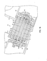
- FIGS. 1A-1B illustrate perspective views of an exemplary semiconductor device 100 in accordance with a first implementation including two suspended-isolating interconnect coils enabling transfer of electrical energy between a first circuit located on a first semiconductor die and a second circuit located on a second semiconductor die.
- the semiconductor device 100 includes a first semiconductor die 110, a second semiconductor die 120, a first isolating block 130, a second isolating block 140, a first interconnect coil 102 having a plurality of wires (shown in dark), and a second interconnect coil 104 having a plurality of wires (shown in light).
- the first and second semiconductor dies 110, 120 provide support for first and second isolating blocks 130, 140, respectively.
- the first isolating block 130 is positioned on first semiconductor die 110 and configured to isolate first semiconductor die 110 from second semiconductor die 120.
- Second isolating block 140 is positioned on second semiconductor die 120 and is configured to isolate second semiconductor die 120 from first semiconductor die 110.
- the semiconductor device 100 includes a first interconnect coil 102 and a second interconnect coil 104.
- the first interconnect coil 102 includes a plurality of wires connecting first semiconductor die 110 to second isolating block 140.
- the second interconnect coil 104 includes a plurality of wires connecting second semiconductor die 120 to first isolating block 130.
- the first and second interconnect coils are mutually positioned to form a transformer inside an IC package.
- the plurality of wires of the second interconnect coil may be adjacent the plurality of wires of the first interconnect coil.
- the plurality of wires of the second interconnect coil may be wrapped around the plurality of wires of the first interconnect coil.
- the plurality of wires of the second interconnect coil may be located inside the plurality of wires of the first interconnect coil.
- FIG. 1B is a top view of the two interconnect coils and the manner in which they connect first semiconductor die 110 to second isolating block 140 and connect second semiconductor die 120 to first isolating block 130.
- the first interconnect coil 102 includes a plurality of wires 150, 152, 154, 156, 158, and 159 connecting first semiconductor die 110 to second isolating block 140.
- the plurality of wires of the first interconnect coil includes a first wire 150 and a second wire 152, at one end connected to each other via a first conductive trace 160 positioned on the top surface of second isolating block 140. The other end is respectively connected to first and second conductive traces 170, 172 positioned on the top surface of first semiconductor die 110.
- the plurality of wires of the first interconnect coil includes a third wire 154 and a fourth wire 156, at one end connected to each other via a second conductive trace 162 positioned on the top surface of second isolating block 140.
- third wire 154 is connected to second wire 152 via second conductive trace 172 positioned on the top surface of first semiconductor die 110 and fourth wire 156 is connected to a third conductive trace 174 positioned on the top surface of first semiconductor die 110.
- the plurality of wires of the first interconnect coil includes a fifth wire 158 and a sixth wire 159, at one end connected to each other via a third conductive trace 164 positioned on the top surface of second isolating block 140 and, at another end fifth wire 158 is connected to fourth wire 156 via third conductive trace 174 positioned on the top surface of first semiconductor die 110 and sixth wire 159 is connected to a fourth conductive trace 176 positioned on the top surface of first semiconductor die 110.
- the second interconnect coil 104 includes a plurality of wires 180, 182, 184, 186, 188, and 189 connecting second semiconductor die 120 to first isolating block 130.
- the plurality of wires of the second interconnect coil includes a first wire 180 and a second wire 182, at one end connected to each other via a first conductive trace 190 positioned on the top surface of first isolating block 130. The other end is respectively connected to first and second conductive traces 196, 197 positioned on the top surface of second semiconductor die 120.
- the plurality of wires of the second interconnect coil includes a third wire 184 and a fourth wire 186, at one end connected to each other via a second conductive trace 192 positioned on the top surface of first isolating block 130.
- third wire 184 is connected to second wire 182 via second conductive trace 197 positioned on the top surface of second semiconductor die 120 and fourth wire 186 is connected to a third conductive trace 198 positioned on the top surface of second semiconductor die 120.
- the plurality of wires of the second interconnect coil includes a fifth wire 188 and a sixth wire 189, at one end connected to each other via a third conductive trace 194 positioned on the top surface of first isolating block 130.
- fifth wire 188 is connected to fourth wire 186 via third conductive trace 198 positioned on the top surface of second semiconductor die 120 and sixth wire 189 is connected to a fourth conductive wire 199 positioned on the top surface of second semiconductor die 120.
- the first and second interconnect coils form a transformer within the IC package, thereby enabling transfer of electrical energy from one circuit to another through the inductively coupled electrical wires.
- the inductively coupled electrical wires can affect such a transfer with, for example, a change in voltage, current, phase or other electric characteristics.
- the first interconnect coil may be connected to a source circuit located on first semiconductor die 110 and the second interconnect coil may be connected to a load circuit located on second semiconductor die 120.
- the alternating current generated from the source circuit enters the first interconnect coil via first conductive trace 170 positioned on first semiconductor die 110 and propagates through its plurality of wires 150, 152, 154, 156, 158, and 159 and returns to first semiconductor die 110 via fourth conductive trace 176.
- This alternating current induces current or voltage on the second interconnect coil connected to the load circuit.
- the induced current or voltage is transferred to the load circuit via first and fourth conductive traces 196, 199 positioned on second semiconductor die 120.
- the conductive traces may include nickel-coated copper, nickel-coated aluminum, or aluminum and provide for electrical connectivity on semiconductor dies 110, 120 and isolating blocks 130, 140, which are generally not conductive.
- the conductive traces may be connected to the plurality of wires via ball bonds, for example.
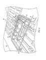
- FIG. 2 illustrates a perspective view of an exemplary semiconductor device 200 including two suspended-isolating interconnect coils enabling transfer of electrical energy between a first circuit located on a first semiconductor die and a printed circuit board located on a lead frame.
- the semiconductor device 200 includes a lead frame 210, a semiconductor die 240, an isolating block 250, a first interconnect coil and a second interconnect coil.
- the lead frame 210 includes a first set of leads (leads 220, 222, 224, and 226) and a second set of leads (leads 230, 232, 234, and 236) which are isolated from each other.
- the semiconductor die 240 is positioned on lead frame 210.
- semiconductor 240 may be positioned on a die pad located on lead frame 210 and may provide a support for isolating block 250.
- the isolating block 250 is positioned on semiconductor die 240 and is configured to isolate semiconductor die 240 from lead frame 210.
- the semiconductor device 200 includes first and second interconnect coils 202, 204.
- the first interconnect coil 202 is formed by a first set of wires (wires 260, 262, 264, and 266), semiconductor die, and the first set of leads (leads 220, 222, 224, and 226).
- the second interconnect coil 204 is formed by a second set of wires (wires 280, 282, 284, and 286), isolating block 250, and the second set of leads (leads 230, 232, 234, and 236).
- the first and second interconnect coils 202, 204 are mutually positioned to form a transformer inside an IC package, thereby enabling a printed circuit board connected to lead frame 210 to communicate with a circuit located on semiconductor die 240.
- the first set of leads includes a first lead 220 and a second lead 222 each of which is conductive and connected to each other at their end tips
- the first set of wires includes a first wire 260 and a second wire 262.
- first and second wires 260, 262 are coupled to each other via first lead 220 and second lead 222 and, at the other end, respectively connected to first and second conductive traces 270, 272 positioned on the top surface of semiconductor die 240.
- another conducing wire 294 may bridge across first and second leads 220, 222.
- the first set of leads further includes a third lead 224 and a fourth lead 226 each of which is conductive and connected to each other at their ends.
- the first set of wires further includes a third wire 264 and a fourth wire 266. At one end, third and fourth wires 264, 266 are connected to each other via third lead 224 and fourth lead 226. At the other end, the third wire is connected to second wire 262 via second conductive trace 272 positioned on the top surface of semiconductor die 240 and fourth wire 266 is connected to a third conductive trace 274 positioned on the top surface of semiconductor die 240.
- the second set of leads includes a first lead 230, a second lead 232, a third lead 234, and a fourth leads 236, each of which is conductive and third and fourth leads 234, 236 connect to each other at their ends.
- the second set of wires includes a first wire 280, a second wire 282, a third wire 284, and a fourth wire 286.
- the first and second wires 280, 282 connect to each other at one end via a first conductive trace 290 positioned on the top surface of isolating block 250. At the other end, first wire 280 connects to first lead 230 and second wire 282 connects to third lead 234.
- third and fourth wires 284, 286 connect to each other at one end via a second conductive trace 292 positioned on the top surface of isolating block 250. At another end, third wire 284 connects to fourth lead 236 and fourth wire 286 connects to second lead 232.
- the first and second interconnect coils form a transformer within the IC package, thereby enabling transfer of electrical energy from one circuit to another through the inductively coupled electrical wires.
- the source circuit may be located on a semiconductor die 240.
- the load circuit may be located on a printed circuit board coupled to a lead frame 210 rather than on a semiconductor die as in FIGS. 1A-1B . As such, a transformer is formed between lead frame 210 and semiconductor die 240.
- the alternating current generated from the source circuit enters the first interconnect coil via first conductive trace 270 positioned on semiconductor die 240 and propagates through its wires 260, 262, 264, and 266 and return to semiconductor die 240 via third conductive trace 274.
- This alternating current induces current or voltage on the second interconnect coil coupled to the load circuit.
- the induced current or voltage is transferred to the load circuit via leads 230, 232.
- the present application removes the coupling away from the silicon surfaces to provide effective isolation while still providing an electrical interconnect.
- the present application can provide for a variation of level of interconnect connectivity based on the number of wires in each interconnect coil. This variation can be set at the time of manufacturing process using inherent wire bonding flexibility. Other implementations are also contemplated.
Landscapes
- Engineering & Computer Science (AREA)
- Power Engineering (AREA)
- Multimedia (AREA)
- Semiconductor Integrated Circuits (AREA)
- Lead Frames For Integrated Circuits (AREA)
- Element Separation (AREA)
- Coils Or Transformers For Communication (AREA)
Abstract
a lead frame including a first set of leads and a second set of leads, the first set of leads being isolated from the second set of leads;
a semiconductor die positioned on the lead frame;
an isolating block positioned on the semiconductor die;
a first interconnect coil formed by a first set of wires, the semiconductor die, and the first set of leads; and
a second interconnect coil isolated from the first interconnect coil and formed by a second set of wires, the isolating block, and the second set of leads.
Description
- The subject matter of this disclosure relates to a suspended isolating interconnect.
- The subject matter of this disclosure, in one implementation, relates to an isolator circuit for providing current and/or voltage isolation inside an integrated circuit ("IC") package. Isolator circuits are used to couple signals between circuits having different ground reference potentials, and to provide ground reference potential isolation inside IC packages. In some applications, different grounds inside IC packages can have a difference in potential as high as several thousand volts.
- Generally, there are three methods for providing isolation between circuits having different ground reference potentials: opto-coupled isolation, transformer-coupled isolation, and capacitively-coupled isolation. Opto-coupled isolation and transformer-coupled isolation are generally disadvantaged in that the coupling devices are relatively bulky and not well suited for use inside an IC package. Capacitors, on the other hand, can be made smaller and be integrated on a semiconductor die.
- However, attempts in the past to provide an isolator circuit on a single semiconductor die have been met with problems due to reliability constraints and damage from electrostatic discharging and over voltage breakdown. In particular, it has been found to be difficult to provide silicon dioxide-based suspended isolating interconnects capable of withstanding the high voltage differential commonly encountered in isolator circuits. Similarly, it has been found to be difficult to increase the voltage on a single semiconductor die to extremely high working voltages (e.g., 2000 volts).
- A semiconductor device is configured to provide current and voltage isolation inside an IC package. In one implementation, the semiconductor device may include first and second semiconductor dies; a first isolating block positioned on the first semiconductor die; and a second isolating block positioned on the second semiconductor die. The semiconductor device may also include a first interconnect coil having a plurality of wires connecting the first semiconductor die to the second isolating block, and a second interconnect coil having a plurality of wires connecting the second semiconductor die to the first isolating block.
- Implementations of the above general aspect may include one or more of the following features. The first and second interconnect coils may be isolated from each other and suspended. Thus, the first and second interconnect coils may be surrounded by a molding compound and may be configured to carry high voltages. The first and second interconnect coils may be mutually positioned such that capacitance coupling is created between the first and second interconnect coils. Alternatively or additionally, the first and second interconnect coils may be mutually positioned to form a transformer in the semiconductor device.
- The first interconnect coil may be connected to a source circuit located on the first semiconductor die and the second interconnect coil may be connected to a load circuit located on the second semiconductor die such that an alternating current applied to the first interconnect coil via the source circuit induces a current or voltage on the second interconnect coil for the load circuit. The plurality of wires of the second interconnect coil may be wrapped around the plurality of wires of the first interconnect coil. Alternatively or additionally, the plurality of wires of the second interconnect coil may be inside the plurality of wires of the first interconnect coil. Alternatively or additionally, the plurality of wires of the second interconnect coil may be adjacent the plurality of wires of the first interconnect coil.
- The plurality of wires of the first interconnect coil may include a first wire and a second wire, at one end connected to each other via a first conductive trace positioned on the top surface of the second isolating block and, at another end respectively connected to first and second conductive traces positioned on the top surface of the first semiconductor die, each of the first wire and second wire connecting the first semiconductor die to the second isolating block. Similarly, the plurality of wires of the second interconnect coil may include a first wire and a second wire, at one end connected to each other via a first conductive trace positioned on the top surface of the first isolating block and, at another end respectively connected to first and second conductive traces positioned on the top surface of the second semiconductor die, each of the first wire and second wire connecting the second semiconductor die to the first isolating block.
- The plurality of wires of the first interconnect coil further may include a third wire and a fourth wire, at one end connected to each other via a second conductive trace positioned on the top surface of the second isolating block and, at another end the third wire may be connected to the second wire via the second conductive trace positioned on the top surface of the first semiconductor die and the fourth wire may be connected to a third conductive trace positioned on the top surface of the first semiconductor die. Similarly, the plurality of wires of the second interconnect coil further may include a third wire and a fourth wire, at one end connected to each other via a second conductive trace positioned on the top surface of the first isolating block and, at another end the third wire may be connected to the second wire via the second conductive trace positioned on the top surface of the second semiconductor die and the fourth wire may be connected to a third conductive trace positioned on the top surface of the second semiconductor die.
- In one implementation, the conductive traces may include nickel-coated copper, nickel-coated aluminum, or aluminum, and the plurality of wires of the first and second interconnect coils may be connected to the conductive traces via ball bonds. The plurality of wires of the first interconnect coil and the plurality of wires of the second interconnect coil may be made of copper, gold, or aluminum.
- In another implementation, the first semiconductor die may include thereon a first circuit and the second semiconductor die may include thereon a second circuit such that the first and second circuits communicate with each other though the first and second interconnect coils.
- In another implementation, a semiconductor device may include a lead frame including a first set of leads and a second set of leads, the first set of leads being isolated from the second set of leads; a semiconductor die positioned on the lead frame; and an isolating block positioned on the semiconductor die. The semiconductor device may also include a first interconnect coil formed by a first set of wires, the die, and the first set of leads; and a second interconnect coil isolated from the first interconnect coil and formed by a second set of wires, the isolating block, and the second set of leads.
- Implementations of the above general aspect may include one or more of the following features. For example, the first and second interconnect coils may be configured to enable a printed circuit board connected to the lead frame to communicate with a circuit located on the semiconductor die. To this end, the first set of leads may include a first lead and a second lead each of which is conductive and connected to the other at its end tip portion, and the first set of wires may include a first wire and a second wire, at one end connected to each other via the first lead and the second lead and, at another end respectively connected to first and second conductive traces positioned on the top surface of the semiconductor die.
- The first set of leads may further include a third lead and a fourth lead each of which is conductive and connected to the other at its end tip portion, and the first set of wires may further include a third wire and a fourth wire, at one end connected to the other via the third lead and the fourth lead and, at another end the third wire is connected to the second wire via the second conductive trace positioned on the top surface of the semiconductor die and the fourth wire is connected to a third conductive trace positioned on the top surface of the semiconductor die.
- Similarly, the second set of leads may include first, second, third, and fourth leads each of which is conductive and the third and fourth leads connect to each other at their end tip portion, the second set of wires may include first, second, third, and fourth wires. In one implementation, the first and second wires, at one end connect to each other via a first conductive trace positioned on the top surface of the isolating block and, at another end the first wire connect to the first lead and the second wire connect to the third lead. Similarly, the third and fourth wires, at one end connect to each other via a second conductive trace positioned on the top surface of the isolating block and, at another end the third wire connect to the fourth lead and the fourth wire connect to second lead.
- The first and second interconnect coils may be isolated from each other and suspended. To isolate the first and second interconnect coils, the first and second interconnect coils may be surrounded by a molding compound. The first and second interconnect coils may be configured to carry high voltages. The first and second interconnect coils may be mutually positioned such that capacitance coupling is created between the first and second interconnect coils.
- The first and second interconnect coils may be mutually positioned to form a transformer in the semiconductor device. To this end, the first set of wires of the first interconnect coil may be adjacent to the second set of wires of the second interconnect coil. For example, the first set of wires of the first interconnect coil may be wrapped around the second set of wires of the second interconnect coil. Alternatively, the first set of wires of the first interconnect coil may be inside the second set of wires of the second interconnect coil.
- The first interconnect coil may be connected to a circuit located on the first semiconductor die and the second interconnect coil may be connected to a printed circuit board connected to the lead frame, such that the first and second interconnect coils enable the printed circuit board to communicate with the circuit located on the semiconductor die. The conductive traces may include nickel-coated copper, nickel-coated aluminum, or aluminum. The first set of wires of the first interconnect coils may be connected to the conductive traces via ball bonds. Similarly, the second set of wires of the second interconnect coils may be connected to the conductive traces via ball bonds. The first set of wires of the first interconnect coil and the second set of wires of the second interconnect coil may be made of copper, gold, or aluminum.
- The details of one or more implementations are set forth in the accompanying drawings and the description below. Other features will be apparent from the description and drawings, and from the claims.
-
-
FIGS. 1A-1B illustrate perspective views of an exemplary semiconductor device including two suspended-isolating interconnect coils enabling transfer of electrical energy between circuits on two semiconductor die. -
FIG. 2 illustrates a perspective view of an exemplary semiconductor device including two suspended-isolating interconnect coils enabling transfer of electrical energy between a circuit on a semiconductor die and a printed circuit board on a lead frame. - In the following detailed description, numerous specific details are set forth by way of examples in order to provide a thorough understanding of the relevant teachings. However, present teachings may be practiced without such details. In other instances, well-known methods, procedures, components, and circuitry have been described at a relatively high-level, without detail, in order to avoid unnecessarily obscuring aspects of the present teachings.
- As is well-known, a transformer is a device that transfers electrical energy from one circuit to another through inductively coupled electrical conductors that affect such a transfer with a change in voltage, current, phase or other electric characteristic. A transformer consists of two or more coils of conducting material, such as wire, wrapped around a core. In particular, it consists of a primary coil and a secondary coil. A changing current applied to the primary coil is transferred to the secondary coil. By adding a load to the secondary coil, one can make the current flow in the transformer, thus transferring electrical energy from one circuit to another.
- Described is a technique and a structure for providing a transformer inside an IC package. In particular, the present disclosure teaches first and second interconnect coils mutually positioned to form a transformer within the IC package. In one implementation, the first and second interconnect coils are mutually positioned such that the first interconnect coil connects a first semiconductor die to an isolating block located on a second semiconductor die, and the second interconnect coil connects the second semiconductor die to an isolating block located on a first semiconductor die. This implementation is described with respect to
FIGS. 1A-1B . - In another implementation, the first and second interconnect coils are mutually positioned such that the first interconnect coil connects a semiconductor die to a lead frame and the second interconnect coil connects the lead frame to an isolating block located on the semiconductor die. The first interconnect coil may be connected to a source circuit located on the semiconductor die. However, in this implementation, the second interconnect coil may be connected to a load circuit located on a printed circuit board connected to the lead frame, such that alternating current applied to the first interconnect coil via the source circuit induces current or voltage on the second interconnect coil connected to the load circuit. This implementation is described with respect to
FIG. 2 . - In each implementation, the first interconnect coil may be connected to a source circuit and the second interconnect coil may be connected to a load circuit. For example, in the first implementation, the first interconnect coil may be connected to a source circuit located on the first semiconductor die and the second interconnect coil may be connected to a load circuit located on the second semiconductor such that an alternating current applied to the first interconnect coil via the source circuit induces current or voltage on the second interconnect coil connected to the load circuit.
-
FIGS. 1A-1B illustrate perspective views of anexemplary semiconductor device 100 in accordance with a first implementation including two suspended-isolating interconnect coils enabling transfer of electrical energy between a first circuit located on a first semiconductor die and a second circuit located on a second semiconductor die. Thesemiconductor device 100 includes a first semiconductor die 110, a second semiconductor die 120, a first isolatingblock 130, a second isolatingblock 140, afirst interconnect coil 102 having a plurality of wires (shown in dark), and asecond interconnect coil 104 having a plurality of wires (shown in light). - The first and second semiconductor dies 110, 120 provide support for first and second isolating
blocks block 130 is positioned on first semiconductor die 110 and configured to isolate first semiconductor die 110 from second semiconductor die 120. Second isolatingblock 140 is positioned on second semiconductor die 120 and is configured to isolate second semiconductor die 120 from first semiconductor die 110. - The
semiconductor device 100 includes afirst interconnect coil 102 and asecond interconnect coil 104. Thefirst interconnect coil 102 includes a plurality of wires connecting first semiconductor die 110 to second isolatingblock 140. Thesecond interconnect coil 104 includes a plurality of wires connecting second semiconductor die 120 to first isolatingblock 130. The first and second interconnect coils are mutually positioned to form a transformer inside an IC package. - To this end, the plurality of wires of the second interconnect coil may be adjacent the plurality of wires of the first interconnect coil. For example, the plurality of wires of the second interconnect coil may be wrapped around the plurality of wires of the first interconnect coil. Alternatively, the plurality of wires of the second interconnect coil may be located inside the plurality of wires of the first interconnect coil.
- To further illustrate,
FIG. 1B is a top view of the two interconnect coils and the manner in which they connect first semiconductor die 110 to second isolatingblock 140 and connect second semiconductor die 120 to first isolatingblock 130. Thefirst interconnect coil 102 includes a plurality ofwires block 140. In particular, the plurality of wires of the first interconnect coil includes afirst wire 150 and asecond wire 152, at one end connected to each other via a firstconductive trace 160 positioned on the top surface of second isolatingblock 140. The other end is respectively connected to first and secondconductive traces - Additionally, the plurality of wires of the first interconnect coil includes a
third wire 154 and afourth wire 156, at one end connected to each other via a secondconductive trace 162 positioned on the top surface of second isolatingblock 140. At the other end,third wire 154 is connected tosecond wire 152 via secondconductive trace 172 positioned on the top surface of first semiconductor die 110 andfourth wire 156 is connected to a thirdconductive trace 174 positioned on the top surface of first semiconductor die 110. Furthermore, the plurality of wires of the first interconnect coil includes afifth wire 158 and asixth wire 159, at one end connected to each other via a thirdconductive trace 164 positioned on the top surface of second isolatingblock 140 and, at another endfifth wire 158 is connected tofourth wire 156 via thirdconductive trace 174 positioned on the top surface of first semiconductor die 110 andsixth wire 159 is connected to a fourthconductive trace 176 positioned on the top surface of first semiconductor die 110. - Similarly, the
second interconnect coil 104 includes a plurality ofwires block 130. In particular, the plurality of wires of the second interconnect coil includes afirst wire 180 and asecond wire 182, at one end connected to each other via a firstconductive trace 190 positioned on the top surface of first isolatingblock 130. The other end is respectively connected to first and secondconductive traces - The plurality of wires of the second interconnect coil includes a
third wire 184 and afourth wire 186, at one end connected to each other via a secondconductive trace 192 positioned on the top surface of first isolatingblock 130. At the other end,third wire 184 is connected tosecond wire 182 via secondconductive trace 197 positioned on the top surface of second semiconductor die 120 andfourth wire 186 is connected to a thirdconductive trace 198 positioned on the top surface of second semiconductor die 120. The plurality of wires of the second interconnect coil includes afifth wire 188 and asixth wire 189, at one end connected to each other via a thirdconductive trace 194 positioned on the top surface of first isolatingblock 130. At the other end,fifth wire 188 is connected tofourth wire 186 via thirdconductive trace 198 positioned on the top surface of second semiconductor die 120 andsixth wire 189 is connected to a fourthconductive wire 199 positioned on the top surface of second semiconductor die 120. - With the foregoing configuration, the first and second interconnect coils form a transformer within the IC package, thereby enabling transfer of electrical energy from one circuit to another through the inductively coupled electrical wires. The inductively coupled electrical wires can affect such a transfer with, for example, a change in voltage, current, phase or other electric characteristics. To illustrate, the first interconnect coil may be connected to a source circuit located on first semiconductor die 110 and the second interconnect coil may be connected to a load circuit located on second semiconductor die 120. The alternating current generated from the source circuit enters the first interconnect coil via first
conductive trace 170 positioned on first semiconductor die 110 and propagates through its plurality ofwires conductive trace 176. This alternating current induces current or voltage on the second interconnect coil connected to the load circuit. The induced current or voltage is transferred to the load circuit via first and fourthconductive traces - The conductive traces may include nickel-coated copper, nickel-coated aluminum, or aluminum and provide for electrical connectivity on semiconductor dies 110, 120 and isolating
blocks - In the second exemplary implementation, a transformer may be formed between a semiconductor die and a lead frame, rather than between two semiconductor dies. In particular,
FIG. 2 illustrates a perspective view of anexemplary semiconductor device 200 including two suspended-isolating interconnect coils enabling transfer of electrical energy between a first circuit located on a first semiconductor die and a printed circuit board located on a lead frame. Thesemiconductor device 200 includes alead frame 210, asemiconductor die 240, an isolatingblock 250, a first interconnect coil and a second interconnect coil. - The
lead frame 210 includes a first set of leads (leads 220, 222, 224, and 226) and a second set of leads (leads 230, 232, 234, and 236) which are isolated from each other. The semiconductor die 240 is positioned onlead frame 210. For example,semiconductor 240 may be positioned on a die pad located onlead frame 210 and may provide a support for isolatingblock 250. The isolatingblock 250 is positioned on semiconductor die 240 and is configured to isolate semiconductor die 240 fromlead frame 210. - The
semiconductor device 200 includes first and second interconnect coils 202, 204. Thefirst interconnect coil 202 is formed by a first set of wires (wires second interconnect coil 204 is formed by a second set of wires (wires block 250, and the second set of leads (leads 230, 232, 234, and 236). - The first and second interconnect coils 202, 204 are mutually positioned to form a transformer inside an IC package, thereby enabling a printed circuit board connected to lead
frame 210 to communicate with a circuit located onsemiconductor die 240. To this end, the first set of leads includes afirst lead 220 and asecond lead 222 each of which is conductive and connected to each other at their end tips, and the first set of wires includes afirst wire 260 and asecond wire 262. At one end, first andsecond wires first lead 220 andsecond lead 222 and, at the other end, respectively connected to first and secondconductive traces conducing wire 294 may bridge across first andsecond leads - In each case, the first set of leads further includes a
third lead 224 and afourth lead 226 each of which is conductive and connected to each other at their ends. The first set of wires further includes athird wire 264 and afourth wire 266. At one end, third andfourth wires third lead 224 andfourth lead 226. At the other end, the third wire is connected tosecond wire 262 via secondconductive trace 272 positioned on the top surface of semiconductor die 240 andfourth wire 266 is connected to a thirdconductive trace 274 positioned on the top surface of semiconductor die 240. - Similarly, the second set of leads includes a
first lead 230, asecond lead 232, athird lead 234, and a fourth leads 236, each of which is conductive and third andfourth leads first wire 280, asecond wire 282, athird wire 284, and afourth wire 286. The first andsecond wires conductive trace 290 positioned on the top surface of isolatingblock 250. At the other end,first wire 280 connects tofirst lead 230 andsecond wire 282 connects tothird lead 234. Similarly, third andfourth wires conductive trace 292 positioned on the top surface of isolatingblock 250. At another end,third wire 284 connects tofourth lead 236 andfourth wire 286 connects tosecond lead 232. - With the foregoing configuration, similar to the first implementation described with respect to
FIGS. 1A-1B , the first and second interconnect coils form a transformer within the IC package, thereby enabling transfer of electrical energy from one circuit to another through the inductively coupled electrical wires. The source circuit may be located on asemiconductor die 240. However and in contrast to the first implementation, the load circuit may be located on a printed circuit board coupled to alead frame 210 rather than on a semiconductor die as inFIGS. 1A-1B . As such, a transformer is formed betweenlead frame 210 and semiconductor die 240. - In each case, the alternating current generated from the source circuit enters the first interconnect coil via first
conductive trace 270 positioned on semiconductor die 240 and propagates through itswires conductive trace 274. This alternating current induces current or voltage on the second interconnect coil coupled to the load circuit. The induced current or voltage is transferred to the load circuit via leads 230, 232. - In the foregoing manners, the present application removes the coupling away from the silicon surfaces to provide effective isolation while still providing an electrical interconnect. Other implementation are contemplated. For example, the present application can provide for a variation of level of interconnect connectivity based on the number of wires in each interconnect coil. This variation can be set at the time of manufacturing process using inherent wire bonding flexibility. Other implementations are also contemplated.
- Further features, aspects and embodiments are provided below in the following clauses:
- Clause 1: A semiconductor device configured to provide current and voltage isolation inside an integrated circuit package, the semiconductor device comprising:
- a first semiconductor die and a second semiconductor die;
- a first isolating block positioned on the first semiconductor die;
- a second isolating block positioned on the second semiconductor die;
- a first interconnect coil having a plurality of wires connecting the first semiconductor die to the second isolating block, and
- a second interconnect coil having a plurality of wires connecting the second semiconductor die to the first isolating block.
- Clause 2: The semiconductor device of clause 1, wherein:
- the plurality of wires of the first interconnect coil includes a first wire and a second wire, at one end connected to each other via a first conductive trace positioned on the top surface of the second isolating block and, at another end respectively connected to first and second conductive traces positioned on the top surface of the first semiconductor die, each of the first wire and second wire connecting the first semiconductor die to the second isolating block, and
- the plurality of wires of the second interconnect coil includes a first wire and a second wire, at one end connected to each other via a first conductive trace positioned on the top surface of the first isolating block and, at another end respectively connected to first and second conductive traces positioned on the top surface of the second semiconductor die, each of the first wire and second wire connecting the second semiconductor die to the first isolating block.
- Clause 3: The semiconductor device of clause 1, wherein the first and second interconnect coils are isolated from each other and suspended.
- Clause 4: The semiconductor device of clause 1, wherein the first and second interconnect coils are surrounded by a molding compound.
- Clause 5: The semiconductor device of clause 1, wherein the first and second interconnect coils are configured to carry high voltages.
- Clause 6: The semiconductor device of clause 1, wherein the first and second interconnect coils are mutually positioned such that capacitance coupling is created between the first and second interconnect coils.
- Clause 7: The semiconductor device of clause 1, wherein the first and second interconnect coils are mutually positioned to form a transformer in the semiconductor device.
- Clause 8: The semiconductor device of clause 1, wherein the first interconnect coil is connected to a source circuit located on the first semiconductor die and the second interconnect coil is connected to a load circuit located on the second semiconductor die such that an alternating current applied to the first interconnect coil via the source circuit induces a current or voltage on the second interconnect coil connected to the load circuit.
- Clause 9: The semiconductor device of clause 1, wherein the plurality of wires of the second interconnect coil is wrapped around the plurality of wires of the first interconnect coil.
- Clause 10: The semiconductor device of clause 1, wherein the plurality of wires of the second interconnect coil is inside the plurality of wires of the first interconnect coil.
- Clause 11: The semiconductor device of clause 1, wherein the plurality of wires of the second interconnect coil is adjacent the plurality of wires of the first interconnect coil.
- Clause 12: The semiconductor device of clause 2, wherein the plurality of wires of the first interconnect coil further includes a third wire and a fourth wire, at one end connected to each other via a second conductive trace positioned on the top surface of the second isolating block and, at another end the third wire is connected to the second wire via the second conductive trace positioned on the top surface of the first semiconductor die and the fourth wire is connected to a third conductive trace positioned on the top surface of the first semiconductor die.
- Clause 13: The semiconductor device of clause 2, wherein the plurality of wires of the second interconnect coil further includes a third wire and a fourth wire, at one end connected to each other via a second conductive trace positioned on the top surface of the first isolating block and, at another end the third wire is connected to the second wire via the second conductive trace positioned on the top surface of the second semiconductor die and the fourth wire is connected to a third conductive trace positioned on the top surface of the second semiconductor die.
- Clause 14: The semiconductor device of clause 2, wherein the conductive traces include nickel-coated copper, nickel-coated aluminum, or aluminum.
- Clause 15: The semiconductor device of clause 2, wherein the plurality of wires of the first and second interconnect coils are connected to the conductive traces via ball bonds.
- Clause 16: The semiconductor device of clause 1, wherein the plurality of wires of the first interconnect coil and the plurality of wires of the second interconnect coil are made of copper, gold, or aluminum.
- Clause 17: The semiconductor device of clause 1, wherein the first semiconductor die includes thereon a first circuit and the second semiconductor die includes thereon a second circuit such that the first and second circuits communicate with each other though the first and second interconnect coils.
- Clause 18: A semiconductor device configured to provide current and voltage isolation inside an integrated circuit package, the semiconductor device comprising:
- a lead frame including a first set of leads and a second set of leads, the first set of leads being isolated from the second set of leads;
- a semiconductor die positioned on the lead frame;
- an isolating block positioned on the semiconductor die;
- a first interconnect coil formed by a first set of wires, the semiconductor die, and the first set of leads; and
- a second interconnect coil isolated from the first interconnect coil and formed by a second set of wires, the isolating block, and the second set of leads.
- Clause 19: The semiconductor device of clause 18, wherein the first and second interconnect coils are configured to enable a printed circuit board connected to the lead frame to communicate with a circuit located on the semiconductor die.
- Clause 20: The semiconductor device of clause 18, wherein:
- the first set of leads includes a first lead and a second lead each of which is conductive and connected to each other at its end tip portion, and
- the first set of wires includes a first wire and a second wire, at one end connected to each other via the first lead and the second lead and, at another end respectively connected to first and second conductive traces positioned on the top surface of the semiconductor die.
- Clause 21: The semiconductor device of clause 20, wherein:
- the first set of leads further includes a third lead and a fourth lead each of which is conductive and connected to each other at its end tip portion, and
- the first set of wires further includes a third wire and a fourth wire, at one end connected to each other via the third lead and the fourth lead and, at another end the third wire is connected to the second wire via the second conductive trace positioned on the top surface of the semiconductor die and the fourth wire is connected to a third conductive trace positioned on the top surface of the semiconductor die.
- Clause 22: The semiconductor device of clause 18, wherein:
- the second set of leads includes first, second, third, and fourth leads each of which is conductive and the third and fourth leads connect to each other at their end tip portion,
- the second set of wires includes first, second, third, and fourth wires,
- the first and second wires, at one end connect to each other via a first conductive trace positioned on the top surface of the isolating block and, at another end the first wire connect to the first lead and the second wire connect to the third lead, and
- the third and fourth wires, at one end connect to each other via a second conductive trace positioned on the top surface of the isolating block and, at another end the third wire connect to the fourth lead and the fourth wire being connected to second lead.
- Clause 23: The semiconductor device of clause 18, wherein the first and second interconnect coils are isolated from each other and suspended.
- Clause 24: The semiconductor device of clause 18, wherein the first and second interconnect coils are surrounded by a molding compound.
- Clause 25: The semiconductor device of clause 18, wherein the first and second interconnect coils are configured to carry high voltages.
- Clause 26: The semiconductor device of clause 18, wherein the first and second interconnect coils are mutually positioned such that capacitance coupling is created between the first and second interconnect coils.
- Clause 27: The semiconductor device of clause 18, wherein the first and second interconnect coils are mutually positioned to form a transformer in the semiconductor device.
- Clause 28: The semiconductor device of clause 18, wherein the first interconnect coil is connected to a circuit located on the first semiconductor die and the second interconnect coil is connected to a printed circuit board connected to the lead frame, such that the first and second interconnect coils enable the printed circuit board to communicate with the circuit located on the semiconductor die.
- Clause 29: The semiconductor device of clause 18, wherein the first set of wires of the first interconnect coil is wrapped around the second set of wires of the second interconnect coil.
- Clause 30: The semiconductor device of clause 18, wherein the first set of wires of the first interconnect coil is inside the second set of wires of the second interconnect coil.
- Clause 31: The semiconductor device of clause 18, wherein the first set of wires of the first interconnect coil is adjacent to the second set of wires of the second interconnect coil.
- Clause 32: The semiconductor device of clause 20, wherein the conductive traces include nickel-coated copper, nickel-coated aluminum, or aluminum.
- Clause 33: The semiconductor device of clause 20, wherein the first set of wires of the first interconnect coils is connected to the conductive traces via ball bonds.
- Clause 34: The semiconductor device of clause 18, wherein the first set of wires of the first interconnect coil and the second set of wires of the second interconnect coil are made of copper, gold, or aluminum.
Claims (15)
- A semiconductor device configured to provide current and voltage isolation inside an integrated circuit package, the semiconductor device comprising:a lead frame including a first set of leads and a second set of leads, the first set of leads being isolated from the second set of leads;a semiconductor die positioned on the lead frame;an isolating block positioned on the semiconductor die;a first interconnect coil formed by a first set of wires, the semiconductor die, and the first set of leads; anda second interconnect coil isolated from the first interconnect coil and formed by a second set of wires, the isolating block, and the second set of leads.
- The semiconductor device of claim 1, wherein
the first set of wires connects the semiconductor die and the first set of leads, and wherein the second set of wires connects the isolating block and the second set of leads. - The semiconductor device of claim 1 or 2, wherein the first and second interconnect coils are configured to enable a printed circuit board connected to the lead frame to communicate with a circuit located on the semiconductor die.
- The semiconductor device of claim 1 or 2, wherein:the first set of leads includes a first lead and a second lead each of which is conductive and connected to each other at its end tip portion, andthe first set of wires includes a first wire and a second wire, at one end connected to each other via the first lead and the second lead and, at another end respectively connected to first and second conductive traces positioned on the top surface of the semiconductor die.
- The semiconductor device of claim 4, wherein:the first set of leads further includes a third lead and a fourth lead each of which is conductive and connected to each other at its end tip portion, andthe first set of wires further includes a third wire and a fourth wire, at one end connected to each other via the third lead and the fourth lead and, at another end the third wire is connected to the second wire via the second conductive trace positioned on the top surface of the semiconductor die and the fourth wire is connected to a third conductive trace positioned on the top surface of the semiconductor die.
- The semiconductor device of claim 1 or 2, wherein:the second set of leads includes first, second, third, and fourth leads each of which is conductive and the third and fourth leads connect to each other at their end tip portion,the second set of wires includes first, second, third, and fourth wires,the first and second wires, at one end connect to each other via a first conductive trace positioned on the top surface of the isolating block and, at another end the first wire connect to the first lead and the second wire connect to the third lead, andthe third and fourth wires, at one end connect to each other via a second conductive trace positioned on the top surface of the isolating block and, at another end the third wire connect to the fourth lead and the fourth wire being connected to second lead.
- The semiconductor device of claim 1 or 2, wherein the first and second interconnect coils are isolated from each other and suspended and/or
wherein the first and second interconnect coils are surrounded by a molding compound and/or
wherein the first and second interconnect coils are configured to carry high voltages. - The semiconductor device of claim 1 or 2, wherein the first and second interconnect coils are mutually positioned such that capacitance coupling is created between the first and second interconnect coils.
- The semiconductor device of claim 1 or 2, wherein the first and second interconnect coils are mutually positioned to form a transformer in the semiconductor device.
- The semiconductor device of claim 1 or 2, wherein the first interconnect coil is connected to a circuit located on the first semiconductor die and the second interconnect coil is connected to a printed circuit board connected to the lead frame, such that the first and second interconnect coils enable the printed circuit board to communicate with the circuit located on the semiconductor die.
- The semiconductor device of claim 1 or 2, wherein the first set of wires of the first interconnect coil is wrapped around the second set of wires of the second interconnect coil, or wherein the first set of wires of the first interconnect coil is inside the second set of wires of the second interconnect coil.
- The semiconductor device of claim 1 or 2, wherein the first set of wires of the first interconnect coil is adjacent to the second set of wires of the second interconnect coil.
- The semiconductor device of claim 4, wherein the conductive traces include nickel-coated copper, nickel-coated aluminum, or aluminum.
- The semiconductor device of claim 4, wherein the first set of wires of the first interconnect coils is connected to the conductive traces via ball bonds.
- The semiconductor device of claim 1 or 2, wherein the first set of wires of the first interconnect coil and the second set of wires of the second interconnect coil are made of copper, gold, or aluminum.
Applications Claiming Priority (2)
| Application Number | Priority Date | Filing Date | Title |
|---|---|---|---|
| US12/202,835 US7902665B2 (en) | 2008-09-02 | 2008-09-02 | Semiconductor device having a suspended isolating interconnect |
| EP09169228.5A EP2159841B1 (en) | 2008-09-02 | 2009-09-02 | A semiconductor device having a suspended isolating interconnect |
Related Parent Applications (3)
| Application Number | Title | Priority Date | Filing Date |
|---|---|---|---|
| EP09169228.5 Division | 2009-09-02 | ||
| EP09169228.5A Division EP2159841B1 (en) | 2008-09-02 | 2009-09-02 | A semiconductor device having a suspended isolating interconnect |
| EP09169228.5A Division-Into EP2159841B1 (en) | 2008-09-02 | 2009-09-02 | A semiconductor device having a suspended isolating interconnect |
Publications (3)
| Publication Number | Publication Date |
|---|---|
| EP2362417A2 true EP2362417A2 (en) | 2011-08-31 |
| EP2362417A3 EP2362417A3 (en) | 2012-05-23 |
| EP2362417B1 EP2362417B1 (en) | 2018-01-10 |
Family
ID=41343288
Family Applications (2)
| Application Number | Title | Priority Date | Filing Date |
|---|---|---|---|
| EP09169228.5A Not-in-force EP2159841B1 (en) | 2008-09-02 | 2009-09-02 | A semiconductor device having a suspended isolating interconnect |
| EP11004204.1A Not-in-force EP2362417B1 (en) | 2008-09-02 | 2009-09-02 | A semiconductor device having a suspended isolating interconnect |
Family Applications Before (1)
| Application Number | Title | Priority Date | Filing Date |
|---|---|---|---|
| EP09169228.5A Not-in-force EP2159841B1 (en) | 2008-09-02 | 2009-09-02 | A semiconductor device having a suspended isolating interconnect |
Country Status (3)
| Country | Link |
|---|---|
| US (1) | US7902665B2 (en) |
| EP (2) | EP2159841B1 (en) |
| TW (1) | TWI463630B (en) |
Families Citing this family (17)
| Publication number | Priority date | Publication date | Assignee | Title |
|---|---|---|---|---|
| US7852186B2 (en) * | 2006-08-28 | 2010-12-14 | Avago Technologies Ecbu Ip (Singapore) Pte. Ltd. | Coil transducer with reduced arcing and improved high voltage breakdown performance characteristics |
| US9019057B2 (en) * | 2006-08-28 | 2015-04-28 | Avago Technologies General Ip (Singapore) Pte. Ltd. | Galvanic isolators and coil transducers |
| US8385043B2 (en) * | 2006-08-28 | 2013-02-26 | Avago Technologies ECBU IP (Singapoare) Pte. Ltd. | Galvanic isolator |
| US9105391B2 (en) * | 2006-08-28 | 2015-08-11 | Avago Technologies General Ip (Singapore) Pte. Ltd. | High voltage hold-off coil transducer |
| US8093983B2 (en) * | 2006-08-28 | 2012-01-10 | Avago Technologies Ecbu Ip (Singapore) Pte. Ltd. | Narrowbody coil isolator |
| US8427844B2 (en) | 2006-08-28 | 2013-04-23 | Avago Technologies Ecbu Ip (Singapore) Pte. Ltd. | Widebody coil isolators |
| US20080278275A1 (en) * | 2007-05-10 | 2008-11-13 | Fouquet Julie E | Miniature Transformers Adapted for use in Galvanic Isolators and the Like |
| US7948067B2 (en) * | 2009-06-30 | 2011-05-24 | Avago Technologies Ecbu Ip (Singapore) Pte. Ltd. | Coil transducer isolator packages |
| US8061017B2 (en) * | 2006-08-28 | 2011-11-22 | Avago Technologies Ecbu Ip (Singapore) Pte. Ltd. | Methods of making coil transducers |
| US7791900B2 (en) * | 2006-08-28 | 2010-09-07 | Avago Technologies General Ip (Singapore) Pte. Ltd. | Galvanic isolator |
| US8258911B2 (en) | 2008-03-31 | 2012-09-04 | Avago Technologies ECBU IP (Singapor) Pte. Ltd. | Compact power transformer components, devices, systems and methods |
| JP5390246B2 (en) * | 2009-04-20 | 2014-01-15 | ルネサスエレクトロニクス株式会社 | Semiconductor device |
| JP2011014576A (en) * | 2009-06-30 | 2011-01-20 | Renesas Electronics Corp | Semiconductor chip, semiconductor wafer and method of manufacturing semiconductor chip |
| US8380146B2 (en) * | 2009-12-31 | 2013-02-19 | Avago Technologies Wireless Ip (Singapore) Pte. Ltd. | Multi-band, multi-mode RF transmit amplifier system with separate signal paths for linear and saturated operation |
| US9136213B2 (en) | 2012-08-02 | 2015-09-15 | Infineon Technologies Ag | Integrated system and method of making the integrated system |
| KR101983165B1 (en) * | 2013-12-26 | 2019-05-28 | 삼성전기주식회사 | Semiconductor package |
| CN111724973A (en) * | 2019-03-18 | 2020-09-29 | 弘邺科技有限公司 | The inductive element is formed in the insulating rubber seat |
Family Cites Families (40)
| Publication number | Priority date | Publication date | Assignee | Title |
|---|---|---|---|---|
| US3922385A (en) | 1973-07-02 | 1975-11-25 | Gen Motors Corp | Solderable multilayer contact for silicon semiconductor |
| US4103267A (en) | 1977-06-13 | 1978-07-25 | Burr-Brown Research Corporation | Hybrid transformer device |
| US4780795A (en) | 1986-04-28 | 1988-10-25 | Burr-Brown Corporation | Packages for hybrid integrated circuit high voltage isolation amplifiers and method of manufacture |
| IT1233008B (en) | 1989-09-21 | 1992-03-14 | Sgs Thomson Microelectronics | INTEGRATED DEVICE WITH PERFECTED CONNECTIONS BETWEEN THE TERMINALS AND THE PLATE OF SEMI-CONDUCTIVE MATERIAL INTEGRATING ELECTRONIC COMPONENTS |
| EP0987758A3 (en) | 1991-12-27 | 2000-05-24 | Fujitsu Limited | Semiconducter device and method of producing the same |
| JPH0653277A (en) | 1992-06-04 | 1994-02-25 | Lsi Logic Corp | Semiconductor device assembly and its assembly method |
| US5444600A (en) * | 1992-12-03 | 1995-08-22 | Linear Technology Corporation | Lead frame capacitor and capacitively-coupled isolator circuit using the same |
| US6284563B1 (en) | 1995-10-31 | 2001-09-04 | Tessera, Inc. | Method of making compliant microelectronic assemblies |
| US5786979A (en) * | 1995-12-18 | 1998-07-28 | Douglass; Barry G. | High density inter-chip connections by electromagnetic coupling |
| US5807767A (en) | 1996-01-02 | 1998-09-15 | Micron Technology, Inc. | Technique for attaching die to leads |
| US5707881A (en) * | 1996-09-03 | 1998-01-13 | Motorola, Inc. | Test structure and method for performing burn-in testing of a semiconductor product wafer |
| US5781077A (en) * | 1997-01-28 | 1998-07-14 | Burr-Brown Corporation | Reducing transformer interwinding capacitance |
| US5952849A (en) * | 1997-02-21 | 1999-09-14 | Analog Devices, Inc. | Logic isolator with high transient immunity |
| US5861662A (en) | 1997-02-24 | 1999-01-19 | General Instrument Corporation | Anti-tamper bond wire shield for an integrated circuit |
| US6242800B1 (en) | 1997-03-12 | 2001-06-05 | International Rectifier Corp. | Heat dissipating device package |
| US6137827A (en) | 1997-04-22 | 2000-10-24 | Silicon Laboratories, Inc. | Isolation system with digital communication across a capacitive barrier |
| US6052289A (en) | 1998-08-26 | 2000-04-18 | Micron Technology, Inc. | Interdigitated leads-over-chip lead frame for supporting an integrated circuit die |
| KR100379835B1 (en) | 1998-12-31 | 2003-06-19 | 앰코 테크놀로지 코리아 주식회사 | Semiconductor Package and Manufacturing Method |
| US6256200B1 (en) | 1999-05-27 | 2001-07-03 | Allen K. Lam | Symmetrical package for semiconductor die |
| JP2001237267A (en) | 2000-02-24 | 2001-08-31 | Sharp Corp | Semiconductor device |
| US6380048B1 (en) | 2001-08-02 | 2002-04-30 | St Assembly Test Services Pte Ltd | Die paddle enhancement for exposed pad in semiconductor packaging |
| US6770982B1 (en) | 2002-01-16 | 2004-08-03 | Marvell International, Ltd. | Semiconductor device power distribution system and method |
| US6703692B1 (en) | 2002-01-31 | 2004-03-09 | Linear Technology Corp. | Leadframe with support members |
| JP2003258180A (en) | 2002-02-27 | 2003-09-12 | Sanyo Electric Co Ltd | Method for manufacturing semiconductor device |
| KR100993579B1 (en) * | 2002-04-30 | 2010-11-10 | 르네사스 일렉트로닉스 가부시키가이샤 | Semiconductor device and electronic device |
| DE10239081B4 (en) | 2002-08-26 | 2007-12-20 | Qimonda Ag | Method for producing a semiconductor device |
| EP2302850A1 (en) | 2003-04-30 | 2011-03-30 | Analog Devices, Inc. | Signal isolators using micro-transformers |
| US7064442B1 (en) | 2003-07-02 | 2006-06-20 | Analog Devices, Inc. | Integrated circuit package device |
| US7002238B2 (en) | 2003-10-23 | 2006-02-21 | Broadcom Corporation | Use of a down-bond as a controlled inductor in integrated circuit applications |
| DE10361696B4 (en) | 2003-12-30 | 2016-03-10 | Infineon Technologies Ag | A method of manufacturing a semiconductor integrated circuit device |
| JP4073876B2 (en) | 2004-01-14 | 2008-04-09 | 三菱電機株式会社 | Semiconductor device |
| US7132314B2 (en) | 2004-05-28 | 2006-11-07 | Texas Instruments Incorporated | System and method for forming one or more integrated circuit packages using a flexible leadframe structure |
| US7447492B2 (en) * | 2004-06-03 | 2008-11-04 | Silicon Laboratories Inc. | On chip transformer isolator |
| US7208818B2 (en) | 2004-07-20 | 2007-04-24 | Alpha And Omega Semiconductor Ltd. | Power semiconductor package |
| US7154165B2 (en) | 2004-07-21 | 2006-12-26 | Linear Technology Corporation | Flashless lead frame with horizontal singulation |
| DE102005020615B4 (en) | 2005-05-03 | 2010-03-11 | Infineon Technologies Austria Ag | Signal transmission arrangement with a transformer and a receiver circuit |
| DE102005034485B4 (en) | 2005-07-20 | 2013-08-29 | Infineon Technologies Ag | Connecting element for a semiconductor device and method for producing a semiconductor power device |
| DE102005047055A1 (en) | 2005-09-30 | 2007-04-05 | Infineon Technologies Austria Ag | Control switch for driving a semiconductor element used as a high-side switch comprises a transformer, a first driver switch, a second driver switch and a rectifier element arranged between supply inputs |
| DE102005054872B4 (en) | 2005-11-15 | 2012-04-19 | Infineon Technologies Ag | Vertical power semiconductor device, semiconductor device and method of making the same |
| SG193796A1 (en) | 2007-07-30 | 2013-10-30 | Stats Chippac Ltd | Semiconductor device and method of providing common voltage bus and wire bondable redistribution |
-
2008
- 2008-09-02 US US12/202,835 patent/US7902665B2/en active Active
-
2009
- 2009-09-01 TW TW098129435A patent/TWI463630B/en active
- 2009-09-02 EP EP09169228.5A patent/EP2159841B1/en not_active Not-in-force
- 2009-09-02 EP EP11004204.1A patent/EP2362417B1/en not_active Not-in-force
Non-Patent Citations (1)
| Title |
|---|
| None |
Also Published As
| Publication number | Publication date |
|---|---|
| EP2362417B1 (en) | 2018-01-10 |
| US7902665B2 (en) | 2011-03-08 |
| TW201017858A (en) | 2010-05-01 |
| US20100052120A1 (en) | 2010-03-04 |
| EP2159841B1 (en) | 2017-11-08 |
| EP2362417A3 (en) | 2012-05-23 |
| EP2159841A3 (en) | 2011-04-27 |
| EP2159841A2 (en) | 2010-03-03 |
| TWI463630B (en) | 2014-12-01 |
Similar Documents
| Publication | Publication Date | Title |
|---|---|---|
| US7902665B2 (en) | Semiconductor device having a suspended isolating interconnect | |
| US8564091B2 (en) | Die-to-die electrical isolation in a semiconductor package | |
| US6998952B2 (en) | Inductive device including bond wires | |
| US7986211B2 (en) | Inductor | |
| CN107818966A (en) | The chip current insulator that single lead frame frame stacks | |
| TWI521668B (en) | Receiver circuit for connector with variable complex impedance | |
| ITMI20111415A1 (en) | MEASUREMENT SYSTEM (PROBE CARD) FOR WIRELESS TESTING (WIRELESS) OF INTEGRATED DEVICES | |
| CN103280441B (en) | For wireless chip-to-chip communications by chip interface (TCI) structure | |
| US6608259B1 (en) | Ground plane for a semiconductor chip | |
| US11270937B2 (en) | Integrated inductor with magnetic mold compound | |
| CN102466739A (en) | probe card | |
| CN107293393A (en) | On-chip transformer Balun | |
| CN104067518A (en) | Driver circuit and method of generating an output signal | |
| Dymond et al. | Probing techniques for gan power electronics: How to obtain 400+ mhz voltage and current measurement bandwidths without compromising pcb layout | |
| ITVI20100341A1 (en) | INDUCTIVE CONNECTION STRUCTURE FOR USE IN AN INTEGRATED CIRCUIT | |
| CN100511640C (en) | Spiral inductance element with multiple lead structure | |
| CN208143194U (en) | Inductors with ESD Protection | |
| JPH10154795A (en) | Inductor on semiconductor chip and its manufacturing method | |
| US11017934B2 (en) | Electronic module | |
| CN113013144A (en) | Novel digital isolator chip | |
| KR102753850B1 (en) | Solder pillar grid array capacitor | |
| TW200834867A (en) | Wire bond integrated circuit package for high speed I/O | |
| US20260026364A1 (en) | Integrated circuit package with star-connected lead | |
| CN202679238U (en) | Power supply module | |
| CN101207098B (en) | Pad structure disposed in semiconductor device and related method |
Legal Events
| Date | Code | Title | Description |
|---|---|---|---|
| PUAI | Public reference made under article 153(3) epc to a published international application that has entered the european phase |
Free format text: ORIGINAL CODE: 0009012 |
|
| AC | Divisional application: reference to earlier application |
Ref document number: 2159841 Country of ref document: EP Kind code of ref document: P |
|
| AK | Designated contracting states |
Kind code of ref document: A2 Designated state(s): AT BE BG CH CY CZ DE DK EE ES FI FR GB GR HR HU IE IS IT LI LT LU LV MC MK MT NL NO PL PT RO SE SI SK SM TR |
|
| RAP1 | Party data changed (applicant data changed or rights of an application transferred) |
Owner name: LINEAR TECHNOLOGY CORPORATION |
|
| REG | Reference to a national code |
Ref country code: DE Ref legal event code: R079 Ref document number: 602009050412 Country of ref document: DE Free format text: PREVIOUS MAIN CLASS: H01L0025070000 Ipc: H01L0023640000 |
|
| PUAL | Search report despatched |
Free format text: ORIGINAL CODE: 0009013 |
|
| AK | Designated contracting states |
Kind code of ref document: A3 Designated state(s): AT BE BG CH CY CZ DE DK EE ES FI FR GB GR HR HU IE IS IT LI LT LU LV MC MK MT NL NO PL PT RO SE SI SK SM TR |
|
| RIC1 | Information provided on ipc code assigned before grant |
Ipc: H01F 19/08 20060101ALI20120417BHEP Ipc: H01L 23/495 20060101ALI20120417BHEP Ipc: H01L 23/64 20060101AFI20120417BHEP |
|
| 17P | Request for examination filed |
Effective date: 20121115 |
|
| 17Q | First examination report despatched |
Effective date: 20150602 |
|
| GRAP | Despatch of communication of intention to grant a patent |
Free format text: ORIGINAL CODE: EPIDOSNIGR1 |
|
| INTG | Intention to grant announced |
Effective date: 20170726 |
|
| GRAS | Grant fee paid |
Free format text: ORIGINAL CODE: EPIDOSNIGR3 |
|
| GRAA | (expected) grant |
Free format text: ORIGINAL CODE: 0009210 |
|
| AC | Divisional application: reference to earlier application |
Ref document number: 2159841 Country of ref document: EP Kind code of ref document: P |
|
| AK | Designated contracting states |
Kind code of ref document: B1 Designated state(s): AT BE BG CH CY CZ DE DK EE ES FI FR GB GR HR HU IE IS IT LI LT LU LV MC MK MT NL NO PL PT RO SE SI SK SM TR |
|
| REG | Reference to a national code |
Ref country code: GB Ref legal event code: FG4D |
|
| REG | Reference to a national code |
Ref country code: AT Ref legal event code: REF Ref document number: 963291 Country of ref document: AT Kind code of ref document: T Effective date: 20180115 Ref country code: CH Ref legal event code: EP |
|
| REG | Reference to a national code |
Ref country code: IE Ref legal event code: FG4D |
|
| REG | Reference to a national code |
Ref country code: NL Ref legal event code: FP |
|
| REG | Reference to a national code |
Ref country code: DE Ref legal event code: R096 Ref document number: 602009050412 Country of ref document: DE |
|
| REG | Reference to a national code |
Ref country code: AT Ref legal event code: MK05 Ref document number: 963291 Country of ref document: AT Kind code of ref document: T Effective date: 20180110 |
|
| PG25 | Lapsed in a contracting state [announced via postgrant information from national office to epo] |
Ref country code: FI Free format text: LAPSE BECAUSE OF FAILURE TO SUBMIT A TRANSLATION OF THE DESCRIPTION OR TO PAY THE FEE WITHIN THE PRESCRIBED TIME-LIMIT Effective date: 20180110 Ref country code: HR Free format text: LAPSE BECAUSE OF FAILURE TO SUBMIT A TRANSLATION OF THE DESCRIPTION OR TO PAY THE FEE WITHIN THE PRESCRIBED TIME-LIMIT Effective date: 20180110 Ref country code: CY Free format text: LAPSE BECAUSE OF FAILURE TO SUBMIT A TRANSLATION OF THE DESCRIPTION OR TO PAY THE FEE WITHIN THE PRESCRIBED TIME-LIMIT Effective date: 20180110 Ref country code: NO Free format text: LAPSE BECAUSE OF FAILURE TO SUBMIT A TRANSLATION OF THE DESCRIPTION OR TO PAY THE FEE WITHIN THE PRESCRIBED TIME-LIMIT Effective date: 20180410 Ref country code: LT Free format text: LAPSE BECAUSE OF FAILURE TO SUBMIT A TRANSLATION OF THE DESCRIPTION OR TO PAY THE FEE WITHIN THE PRESCRIBED TIME-LIMIT Effective date: 20180110 Ref country code: ES Free format text: LAPSE BECAUSE OF FAILURE TO SUBMIT A TRANSLATION OF THE DESCRIPTION OR TO PAY THE FEE WITHIN THE PRESCRIBED TIME-LIMIT Effective date: 20180110 |
|
| REG | Reference to a national code |
Ref country code: FR Ref legal event code: PLFP Year of fee payment: 10 |
|
| PG25 | Lapsed in a contracting state [announced via postgrant information from national office to epo] |
Ref country code: SE Free format text: LAPSE BECAUSE OF FAILURE TO SUBMIT A TRANSLATION OF THE DESCRIPTION OR TO PAY THE FEE WITHIN THE PRESCRIBED TIME-LIMIT Effective date: 20180110 Ref country code: IS Free format text: LAPSE BECAUSE OF FAILURE TO SUBMIT A TRANSLATION OF THE DESCRIPTION OR TO PAY THE FEE WITHIN THE PRESCRIBED TIME-LIMIT Effective date: 20180510 Ref country code: BG Free format text: LAPSE BECAUSE OF FAILURE TO SUBMIT A TRANSLATION OF THE DESCRIPTION OR TO PAY THE FEE WITHIN THE PRESCRIBED TIME-LIMIT Effective date: 20180410 Ref country code: LV Free format text: LAPSE BECAUSE OF FAILURE TO SUBMIT A TRANSLATION OF THE DESCRIPTION OR TO PAY THE FEE WITHIN THE PRESCRIBED TIME-LIMIT Effective date: 20180110 Ref country code: AT Free format text: LAPSE BECAUSE OF FAILURE TO SUBMIT A TRANSLATION OF THE DESCRIPTION OR TO PAY THE FEE WITHIN THE PRESCRIBED TIME-LIMIT Effective date: 20180110 Ref country code: GR Free format text: LAPSE BECAUSE OF FAILURE TO SUBMIT A TRANSLATION OF THE DESCRIPTION OR TO PAY THE FEE WITHIN THE PRESCRIBED TIME-LIMIT Effective date: 20180411 Ref country code: PL Free format text: LAPSE BECAUSE OF FAILURE TO SUBMIT A TRANSLATION OF THE DESCRIPTION OR TO PAY THE FEE WITHIN THE PRESCRIBED TIME-LIMIT Effective date: 20180110 |
|
| REG | Reference to a national code |
Ref country code: DE Ref legal event code: R097 Ref document number: 602009050412 Country of ref document: DE |
|
| PG25 | Lapsed in a contracting state [announced via postgrant information from national office to epo] |
Ref country code: EE Free format text: LAPSE BECAUSE OF FAILURE TO SUBMIT A TRANSLATION OF THE DESCRIPTION OR TO PAY THE FEE WITHIN THE PRESCRIBED TIME-LIMIT Effective date: 20180110 Ref country code: RO Free format text: LAPSE BECAUSE OF FAILURE TO SUBMIT A TRANSLATION OF THE DESCRIPTION OR TO PAY THE FEE WITHIN THE PRESCRIBED TIME-LIMIT Effective date: 20180110 |
|
| PLBE | No opposition filed within time limit |
Free format text: ORIGINAL CODE: 0009261 |
|
| STAA | Information on the status of an ep patent application or granted ep patent |
Free format text: STATUS: NO OPPOSITION FILED WITHIN TIME LIMIT |
|
| PG25 | Lapsed in a contracting state [announced via postgrant information from national office to epo] |
Ref country code: SK Free format text: LAPSE BECAUSE OF FAILURE TO SUBMIT A TRANSLATION OF THE DESCRIPTION OR TO PAY THE FEE WITHIN THE PRESCRIBED TIME-LIMIT Effective date: 20180110 Ref country code: CZ Free format text: LAPSE BECAUSE OF FAILURE TO SUBMIT A TRANSLATION OF THE DESCRIPTION OR TO PAY THE FEE WITHIN THE PRESCRIBED TIME-LIMIT Effective date: 20180110 Ref country code: SM Free format text: LAPSE BECAUSE OF FAILURE TO SUBMIT A TRANSLATION OF THE DESCRIPTION OR TO PAY THE FEE WITHIN THE PRESCRIBED TIME-LIMIT Effective date: 20180110 Ref country code: DK Free format text: LAPSE BECAUSE OF FAILURE TO SUBMIT A TRANSLATION OF THE DESCRIPTION OR TO PAY THE FEE WITHIN THE PRESCRIBED TIME-LIMIT Effective date: 20180110 |
|
| 26N | No opposition filed |
Effective date: 20181011 |
|
| PG25 | Lapsed in a contracting state [announced via postgrant information from national office to epo] |
Ref country code: SI Free format text: LAPSE BECAUSE OF FAILURE TO SUBMIT A TRANSLATION OF THE DESCRIPTION OR TO PAY THE FEE WITHIN THE PRESCRIBED TIME-LIMIT Effective date: 20180110 |
|
| PG25 | Lapsed in a contracting state [announced via postgrant information from national office to epo] |
Ref country code: MC Free format text: LAPSE BECAUSE OF FAILURE TO SUBMIT A TRANSLATION OF THE DESCRIPTION OR TO PAY THE FEE WITHIN THE PRESCRIBED TIME-LIMIT Effective date: 20180110 |
|
| REG | Reference to a national code |
Ref country code: CH Ref legal event code: PL |
|
| REG | Reference to a national code |
Ref country code: BE Ref legal event code: MM Effective date: 20180930 |
|
| REG | Reference to a national code |
Ref country code: IE Ref legal event code: MM4A |
|
| PG25 | Lapsed in a contracting state [announced via postgrant information from national office to epo] |
Ref country code: LU Free format text: LAPSE BECAUSE OF NON-PAYMENT OF DUE FEES Effective date: 20180902 |
|
| PG25 | Lapsed in a contracting state [announced via postgrant information from national office to epo] |
Ref country code: IE Free format text: LAPSE BECAUSE OF NON-PAYMENT OF DUE FEES Effective date: 20180902 |
|
| PG25 | Lapsed in a contracting state [announced via postgrant information from national office to epo] |
Ref country code: CH Free format text: LAPSE BECAUSE OF NON-PAYMENT OF DUE FEES Effective date: 20180930 Ref country code: BE Free format text: LAPSE BECAUSE OF NON-PAYMENT OF DUE FEES Effective date: 20180930 Ref country code: LI Free format text: LAPSE BECAUSE OF NON-PAYMENT OF DUE FEES Effective date: 20180930 |
|
| PG25 | Lapsed in a contracting state [announced via postgrant information from national office to epo] |
Ref country code: MT Free format text: LAPSE BECAUSE OF NON-PAYMENT OF DUE FEES Effective date: 20180902 |
|
| PG25 | Lapsed in a contracting state [announced via postgrant information from national office to epo] |
Ref country code: TR Free format text: LAPSE BECAUSE OF FAILURE TO SUBMIT A TRANSLATION OF THE DESCRIPTION OR TO PAY THE FEE WITHIN THE PRESCRIBED TIME-LIMIT Effective date: 20180110 |
|
| PG25 | Lapsed in a contracting state [announced via postgrant information from national office to epo] |
Ref country code: HU Free format text: LAPSE BECAUSE OF FAILURE TO SUBMIT A TRANSLATION OF THE DESCRIPTION OR TO PAY THE FEE WITHIN THE PRESCRIBED TIME-LIMIT; INVALID AB INITIO Effective date: 20090902 Ref country code: PT Free format text: LAPSE BECAUSE OF FAILURE TO SUBMIT A TRANSLATION OF THE DESCRIPTION OR TO PAY THE FEE WITHIN THE PRESCRIBED TIME-LIMIT Effective date: 20180110 |
|
| PG25 | Lapsed in a contracting state [announced via postgrant information from national office to epo] |
Ref country code: MK Free format text: LAPSE BECAUSE OF NON-PAYMENT OF DUE FEES Effective date: 20180110 |
|
| REG | Reference to a national code |
Ref country code: DE Ref legal event code: R082 Ref document number: 602009050412 Country of ref document: DE Representative=s name: WITHERS & ROGERS LLP, DE Ref country code: DE Ref legal event code: R082 Ref document number: 602009050412 Country of ref document: DE Representative=s name: MUELLER-BORE & PARTNER PATENTANWAELTE PARTG MB, DE Ref country code: DE Ref legal event code: R081 Ref document number: 602009050412 Country of ref document: DE Owner name: ANALOG DEVICES INTERNATIONAL UNLIMITED COMPANY, IE Free format text: FORMER OWNER: LINEAR TECHNOLOGY CORPORATION, MILPITAS, CALIF., US |
|
| REG | Reference to a national code |
Ref country code: DE Ref legal event code: R082 Ref document number: 602009050412 Country of ref document: DE Representative=s name: WITHERS & ROGERS LLP, DE |
|
| PGFP | Annual fee paid to national office [announced via postgrant information from national office to epo] |
Ref country code: IT Payment date: 20210824 Year of fee payment: 13 |
|
| REG | Reference to a national code |
Ref country code: GB Ref legal event code: 732E Free format text: REGISTERED BETWEEN 20211202 AND 20211209 |
|
| REG | Reference to a national code |
Ref country code: NL Ref legal event code: PD Owner name: ANALOG DEVICES INTERNATIONAL UNLIMITED COMPANY; IE Free format text: DETAILS ASSIGNMENT: CHANGE OF OWNER(S), ASSIGNMENT; FORMER OWNER NAME: LINEAR TECHNOLOGY LLC Effective date: 20211216 |
|
| PGFP | Annual fee paid to national office [announced via postgrant information from national office to epo] |
Ref country code: NL Payment date: 20230822 Year of fee payment: 15 |
|
| PG25 | Lapsed in a contracting state [announced via postgrant information from national office to epo] |
Ref country code: IT Free format text: LAPSE BECAUSE OF NON-PAYMENT OF DUE FEES Effective date: 20220902 |
|
| PGFP | Annual fee paid to national office [announced via postgrant information from national office to epo] |
Ref country code: GB Payment date: 20230823 Year of fee payment: 15 |
|
| PGFP | Annual fee paid to national office [announced via postgrant information from national office to epo] |
Ref country code: FR Payment date: 20230822 Year of fee payment: 15 Ref country code: DE Payment date: 20230822 Year of fee payment: 15 |
|
| REG | Reference to a national code |
Ref country code: DE Ref legal event code: R119 Ref document number: 602009050412 Country of ref document: DE |
|
| REG | Reference to a national code |
Ref country code: NL Ref legal event code: MM Effective date: 20241001 |
|
| GBPC | Gb: european patent ceased through non-payment of renewal fee |
Effective date: 20240902 |
|
| PG25 | Lapsed in a contracting state [announced via postgrant information from national office to epo] |
Ref country code: NL Free format text: LAPSE BECAUSE OF NON-PAYMENT OF DUE FEES Effective date: 20241001 |
|
| PG25 | Lapsed in a contracting state [announced via postgrant information from national office to epo] |
Ref country code: DE Free format text: LAPSE BECAUSE OF NON-PAYMENT OF DUE FEES Effective date: 20250401 |
|
| PG25 | Lapsed in a contracting state [announced via postgrant information from national office to epo] |
Ref country code: GB Free format text: LAPSE BECAUSE OF NON-PAYMENT OF DUE FEES Effective date: 20240902 |
|
| PG25 | Lapsed in a contracting state [announced via postgrant information from national office to epo] |
Ref country code: FR Free format text: LAPSE BECAUSE OF NON-PAYMENT OF DUE FEES Effective date: 20240930 |