EP2360753A1 - Organic electroluminescence element - Google Patents
Organic electroluminescence element Download PDFInfo
- Publication number
- EP2360753A1 EP2360753A1 EP09833497A EP09833497A EP2360753A1 EP 2360753 A1 EP2360753 A1 EP 2360753A1 EP 09833497 A EP09833497 A EP 09833497A EP 09833497 A EP09833497 A EP 09833497A EP 2360753 A1 EP2360753 A1 EP 2360753A1
- Authority
- EP
- European Patent Office
- Prior art keywords
- light
- layer
- light emission
- emission layer
- electroluminescence element
- Prior art date
- Legal status (The legal status is an assumption and is not a legal conclusion. Google has not performed a legal analysis and makes no representation as to the accuracy of the status listed.)
- Withdrawn
Links
Images




Classifications
-
- H—ELECTRICITY
- H10—SEMICONDUCTOR DEVICES; ELECTRIC SOLID-STATE DEVICES NOT OTHERWISE PROVIDED FOR
- H10K—ORGANIC ELECTRIC SOLID-STATE DEVICES
- H10K50/00—Organic light-emitting devices
- H10K50/80—Constructional details
- H10K50/85—Arrangements for extracting light from the devices
-
- H—ELECTRICITY
- H10—SEMICONDUCTOR DEVICES; ELECTRIC SOLID-STATE DEVICES NOT OTHERWISE PROVIDED FOR
- H10K—ORGANIC ELECTRIC SOLID-STATE DEVICES
- H10K50/00—Organic light-emitting devices
- H10K50/80—Constructional details
- H10K50/85—Arrangements for extracting light from the devices
- H10K50/854—Arrangements for extracting light from the devices comprising scattering means
-
- H—ELECTRICITY
- H10—SEMICONDUCTOR DEVICES; ELECTRIC SOLID-STATE DEVICES NOT OTHERWISE PROVIDED FOR
- H10K—ORGANIC ELECTRIC SOLID-STATE DEVICES
- H10K50/00—Organic light-emitting devices
- H10K50/80—Constructional details
- H10K50/805—Electrodes
- H10K50/81—Anodes
- H10K50/818—Reflective anodes, e.g. ITO combined with thick metallic layers
-
- H—ELECTRICITY
- H10—SEMICONDUCTOR DEVICES; ELECTRIC SOLID-STATE DEVICES NOT OTHERWISE PROVIDED FOR
- H10K—ORGANIC ELECTRIC SOLID-STATE DEVICES
- H10K50/00—Organic light-emitting devices
- H10K50/80—Constructional details
- H10K50/805—Electrodes
- H10K50/82—Cathodes
- H10K50/828—Transparent cathodes, e.g. comprising thin metal layers
-
- H—ELECTRICITY
- H10—SEMICONDUCTOR DEVICES; ELECTRIC SOLID-STATE DEVICES NOT OTHERWISE PROVIDED FOR
- H10K—ORGANIC ELECTRIC SOLID-STATE DEVICES
- H10K50/00—Organic light-emitting devices
- H10K50/80—Constructional details
- H10K50/85—Arrangements for extracting light from the devices
- H10K50/856—Arrangements for extracting light from the devices comprising reflective means
-
- H—ELECTRICITY
- H10—SEMICONDUCTOR DEVICES; ELECTRIC SOLID-STATE DEVICES NOT OTHERWISE PROVIDED FOR
- H10K—ORGANIC ELECTRIC SOLID-STATE DEVICES
- H10K2102/00—Constructional details relating to the organic devices covered by this subclass
- H10K2102/301—Details of OLEDs
- H10K2102/351—Thickness
Definitions
- This invention relates to organic electroluminescence elements which are used for a lighting source, a backlight for the liquid crystal display instrument, and a flat panel display. Specifically, this invention relates to the organic electroluminescence elements which are designed on the basis of the adequate optical design to have a good light emitting property when the light scattering region is provided on the outer surface of the light transmissive substrate, which is defined as a part of the organic electroluminescence element.
- Fig. 6 shows one example of the structure of the organic electroluminescence element.
- the organic electroluminescence element comprises a light transmissive substrate 6, a light transmissive electrode 1 which is defined as an anode, a hole transport layer 8, a light emission layer 3, an electron transport layer 9, and a light reflective electrode 2 defined as a cathode.
- the light transmissive electrode 1, the hole transport layer 8, the light emission layer 3, the electron transport layer 9, a light reflective electrode 2 are provided on the upper surface of the light transmissive substrate 6 such that the light transmissive electrode 1, the hole transport layer 8, the light emission layer 3, the electron transport layer 9, a light reflective electrode 2 are arranged in order.
- Such the organic electroluminescence element has a property of emitting the light by itself.
- the organic electroluminescence element has a light emission property of comparatively high efficiency.
- the organic electroluminescence element has a property of emitting the light having various colors.
- the organic electroluminescence element is expected to be used for the luminous body for the display device such as flat panel display, a light source such as a backlight of the liquid crystal display, and a lighting device. In addition, a part of the organic electroluminescence element is practically used.
- the organic electroluminescence element is a thin film device having a thickness which is approximately same as an order of the optical wavelength.
- the organic electroluminescence element has the thickness which is correlated with the light emission property.
- the device structure of the electroluminescence element to have the design of the film design which is suitable for both the electrical design and the optical design.
- the organic electroluminescence element when the organic electroluminescence element generates the light in the light emission layer 3 of the organic electroluminescence, the light is totally reflected by the light emission layer 3, the organic layer 4, inside of the electrode, and the inside of the substrate 6, whereby the light generated in the organic electroluminescence element is confined in the light emission layer 3, the organic layer 4, inside of the electrode, and the inside of the substrate 6.
- the light emission layer 3 when the light emission layer 3 generates the light, 50 percents of the light generated in the light emission layer 3 is confined in the inside of light emission layer 3, the inside of the organic layer 4, and the inside of the light transparent electrode 1.
- 30 percents of the light generated in the light emission layer 3 is confined in the inside of the substrate 6. Therefore, the an amount of the light which is emitted to the outside is only 20 percents of the total amount.
- the substrate 6 that the light scattering region 7 is disposed on the outer surface of the substrate 6.
- the light scattering region 7 allows a part of the light confined in the substrate 6 to be extracted to the outside of the organic electroluminescence element. This configuration makes it possible to increase an amount of the light which is extracted to the outside of the organic electroluminescence element.
- Fig. 1 it is well known to employ the light transmissive electrode 1 and the substrate 6 with a light scattering region 7 between the light transmissive electrode 1 and the substrate 6.
- a part of the light which is confined in the light emission layer 3, the organic layer 4, and the light transmissive electrode 1 is extracted from the organic electroluminescence element.
- an amount of the light which is confined in the light emission layer 3, the organic layer 4, and the light transmissive electrode 1 is greater than an amount of the light which is confined in the substrate 6.
- the organic electroluminescence element comprises the light transmissive electrode 1 and the substrate 6 with the light scattering region 7 between the light transmissive electrode 1 and the substrate 6 is configured to emit the light having an amount which is greater than an amount of the light which is emitted from the organic electroluminescence element comprising the substrate 6 with the light scattering region 7 on the outer surface of the substrate 6.
- the organic electroluminescence element having a designing of the distance between the luminous point in the light emission layer 3 and the light transmissive electrode 2 in order to increase an amount of the light which is given off to the outside of the organic electroluminescence element.
- the organic electroluminescence element disclosed in the patent literature 1 has a luminous point and the light transmissive electrode 1 to create a distance between the luminous point and the light transmissive electrode 1; the distance between the luminous point and the light transmissive electrode 1 is approximately equal to an even multiple of the one-quarter of the wavelength.
- the organic electroluminescence element has the luminous point and the light reflective electrode 2 to create a distance which is approximately equal to an odd multiple of one-quarter of the wavelength.
- the patent literature 2 discloses the electroluminescence element comprising the electrodes which are arranged to create the distance between the electrodes; the distance is determined on the basis of the phase shift of the light.
- the patent literature 3 disclose the organic electroluminescence element comprising the light transmissive electrode 1 and the light reflective electrode 2 which are arranged to create the distance between the light transmissive electrode 1 and the light reflective electrode; the distance is set within a predetermined range which is determined on the basis of the phase shift of the light in the light reflective electrode 2.
- each one of the patent literature 4 and the patent literature 5 discloses the organic electroluminescence element which comprises the substrate 6 with the light scattering region 7, and the electrodes which are arranged to create the distance between the electrodes; the distance between the electrodes are determined to have a predetermined value.
- each one of the patent literatures discloses that the organic electroluminescence element has the luminescence efficiency which is greatly related to the thickness of the light transparent film which constitutes the organic electroluminescence element.
- each the patent literature discloses to employ the luminous point and the light reflective electrode 2 with "the film having a particular optical thickness" between the luminous point and the light reflective electrode 2 in order to obtain the good efficiency under a condition where the particular optical thickness satisfies the following exemplified formula. "The particular optical thickness is equal to (2m+1)/4 multiple of the luminous wavelength (m is an integer number and is more than zero).
- the patent literature 1 fails to disclose the consideration of the phase shift of the light in the light reflective electrode 2.
- the patent literature 2 discloses the target spectrum; the half width of the spectrum is limited to be equal to or less than 50 nanometers.
- the patent literature 3 only defines the distance between the electrodes.
- the patent literature 3 discloses no definition of the distance between the luminous point and the light reflective electrode 2.
- each one of the patent literatures 1 to 3 discloses the optical designing of the organic electroluminescence element which employs the substrate and other members without light scattering region 7 on the substrate and other members.
- each one of the patent literatures 4 and 5 discloses the organic electroluminescence element which comprises the light scattering region 7.
- each one of the patent literatures 4 and 5 only disclose only the definition of satisfying the above formula under a condition where the "m" is equal to zero. Therefore, it is impossible to apply the technical feature of the above to the situation where there is a necessity to arrange the light emission layer 3 and the light reflective electrode 2 to create the distance of a certain level between the light emission layer 3 and the light reflective electrode 2. This is similar to the patent literature 2.
- the applicant of this application discloses the appropriate distance between the luminous point and the light reflective electrode 2 in a case where the light scattering region 7 is disposed on the outer surface of the substrate 6 shown in Fig. 7 and where there is a need to create the distance between the light emission layer 3 and the light reflective electrode 2, with respect to arbitral luminescence spectrum.
- the organic electroluminescence element comprising the light scattering region 7 between the light transmissive electrode 3 and the substrate 6 emits the light which has an amount which is greater than an amount of the organic electroluminescence element comprising a light scattering region 7 on the outer surface of the substrate 6.
- the organic electroluminescence element having this configuration a design principle of the suitable distance between the luminous point and the light reflective electrode 2 under a situation where a certain distance is needed between the light emission layer 3 and the light reflective electrode 2 with respect to the arbitral emission spectrum is not cleared.
- an organic electroluminescence element of new type shown in Fig. 2 comprises a plurality of the light emission layers 3 and a charge supply layer 10 which is disposed between the light emission layers 3; the charge supply layer 10 comprises a light transmissive electrode, and a charge generation layer which comprises layers such as a an organic semiconductor, an inorganic semiconductor, an electron accepting material, and an electron releasing material.
- a plurality of the light emission layer 3 are stacked along a thickness direction of the organic electroluminescence element.
- the organic electroluminescence element of the above type has a possibility of emitting the light having a high brightness, and of long operating life, whereby the organic electroluminescence element of the above type is highly expected its future progress.
- the principle of the optical design for the future progress is not clear yet.
- An object in this invention is to produce an organic electroluminescence element having a good light emitting property.
- the organic electroluminescence element is produced on the basis of the adequate optical designing, whereby the organic electroluminescence element comprises a light transmissive electrode, a light transmissive substrate, and a light scattering region which is located in a position between the light transmissive electrode and the light transmissive substrate; the position of the light scattering region is determined on the basis of the adequate optical designing.
- the organic electroluminescence element in this invention comprises a light transmissive electrode, a light reflective electrode, an organic light emission layer, a light scattering layer, and a light transmissive substrate.
- the organic light emission layer comprises a light emission layer which comprises a a luminescent material.
- the organic light emission layer has a first surface and a second surface which is opposite of the first surface from the organic light emission layer.
- the light reflective electrode is disposed on the first surface.
- the light transmissive electrode is disposed on the second surface.
- the light scattering layer is disposed on the light transmissive electrode.
- the light transmissive substrate is disposed on the light scattering layer.
- the light reflective electrode is separated from the luminous point of the light emission layer by "d".
- ⁇ is defined by a wavelength of a predetermined light which is emitted from the light emission layer.
- n is a refractive index of a layer which is located between the luminous point and the light reflective electrode at the light having the wavelength " ⁇ ”.
- n1 is a refractive index of a layer which is located between the luminous point of the light emission layer and the light reflective electrode and which is in contact with the light reflective electrode, at the light having the wavelength " ⁇ ”.
- k1 is an extinction coefficient of the layer which is located between the luminous point of the light emission layer and the light reflective electrode and which is in contact with the light reflective electrode, at the light having the wavelength " ⁇ ".
- n2 is a refractive index of the light reflective electrode at the wavelength " ⁇ " of the light.
- k2 is an extinction coefficient of the light reflective electrode at the light having the wavelength " ⁇ ”.
- m is equal to 0 or 1.
- "a” satisfies a following formula. - 1.17 ⁇ n org / n EML + 1.94 ⁇ a ⁇ - 0.16 ⁇ n org / n EML + 2.33
- "a” satisfies a following formula 0.28 ⁇ n org / n EML + 0.75 ⁇ a ⁇ 2.85 ⁇ n org / n EML - 1.23
- the wavelength ⁇ of a predetermined light satisfies a condition where a product being obtained by multiplying a spectral radiant flux of the photoluminescence spectrum of the predetermined light and the CIE standard luminosity factor has maximum.
- the wavelength ⁇ satisfies a condition where a quotient which is obtained by dividing the spectral radiant flux of the photoluminescence spectrum of a predetermined light by a photon energy of each the energy has a maximum.
- the organic light emission layer has two light emission layers.
- the distance between the luminous point of each the light emission layer and the first electrode is defined by "d".
- Fig. 1 shows one example of a configuration of the organic electroluminescence element.
- the organic electroluminescence element comprises a light transmissive substrate 6 , a light scattering layer 7 , a light transmissive electrode 1 , an organic light emission layer 5, and a light reflective electrode 2 .
- the light scattering layer 7 is disposed on the light transmissive substrate 6 .
- the light transmissive electrode 1 is disposed on the light scattering layer 7 .
- the organic light emission layer 5 is disposed on the light transmissive electrode 1 .
- the light reflective electrode 2 is disposed on the organic light emission layer 5 . Therefore, the light reflective electrode 2 is disposed on the lower surface of the organic light emission layer 5 .
- the light reflective electrode 2 is disposed on the first surface of the organic light emission layer 5 .
- the light transmissive electrode 1 is disposed on the upper surface of the organic light emission layer 5 .
- the light transmissive electrode 1 id disposed on the second surface of the organic light emission layer 5 .
- the light scattering layer 7 , the light transmissive electrode 1 , the organic light emission layer 5 , and the light reflective electrode 2 are stacked on the light transmissive substrate 6 such that the light scattering layer 7 , the light transmissive electrode 1 , the organic light emission layer 5 , and the light reflective electrode 2 are arranged in order.
- the organic light emission layer 5 comprises a light emission layer 3 which is made of luminescence material.
- the organic light emission layer comprises an organic layer 4 arbitrarily; the organic layer 4 is exemplified by a charge injection layer, the charge transport layer 9 , the hole blocking layer, the hole injection layer, the hole transport layer 8 which are stacked.
- the charge transport layer 9 is interposed between the light reflective electrode 2 and the light emission layer 3 .
- the hole transport layer 8 is interposed between the light transmissive electrode and the light emission layer 3 . It is noted that a plurality of the light emission layer 3 on the light emission layer may be employed as the light emission layer which is explained in the above.
- the organic light emission layer 5 receives the voltage, the light emission layer emits the light.
- the light reflective electrode 2 is configured to reflect the light which is emitted from the organic light emission layer 5 .
- the light transmissive electrode 1 is configured to transmit the light which is emitted from the light emission layer 5 .
- the light transmissive electrode 1 is configured to transmit the light which is firstly emitted from the organic light emission layer 5 and is then reflected by the light reflective electrode 2 .
- the light which is transmitted through the light transmissive electrode 1 is scattered by the light scattering layer 7 .
- the light transmissive substrate 6 is configured to transmit the light which is scattered by the light scattering layer 7 . In this manner, the organic electroluminescence element emits the light.
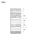
- Fig. 2 shows one example of the electroluminescence element which comprises two light emission layer 3
- the light scattering layer 7 is disposed on the light transmissive substrate 6 .
- the light transmissive electrode 1 is disposed on the light scattering layer 7 .
- a first organic light emission layer 5 is disposed on the light transmissive electrode 1 .
- the charge supply layer 10 is disposed on the first organic light emission layer.
- a second organic light emission layer 5 is disposed on the charge supply layer 10 .
- the light reflective electrode 2 is disposed on the second organic light emission layer 5 .
- each one of the organic light emission layer 5 comprises the light emission layer 3 which includes the luminescence material.
- each one of the organic light emission layer 5 comprises the organic layer 4 , arbitrarily; the organic layer 4 comprises the charge injection layer, the charge transport layer 9 , the hole blocking layer, the hole injection layer, and the hole transport layer 8 . Therefore, the organic electroluminescence element shown in Fig. 2 may be considered to have one organic light emission layer comprising a plurality of the light emission layers.
- the light reflective electrode 2 is located on a same side of the organic light emission layer 5 as the charge transport layer 9 .
- the hole transport layer 8 is disposed on the same side of the organic light emission layer 5 as the light transmissive electrode 1 .
- the organic electroluminescence element may comprises a plurality of the light emission layers 3 .
- a plurality of the charge supply layer 10 is interposed between the light transmissive electrode 1 and the light reflective electrode 2 .
- the organic light emission layer 5 is interposed between the light transmissive electrode 1 and the charge supply layer 10 .
- the organic light emission layer is interposed between the charge supply layer 10 and the light reflective electrode 2 .
- the organic electroluminescence elements are constituted according to the above. In addition, it is possible to stack a plurality of the light emission layers in the organic light emission layer 5 . When a plurality of the light emission layers 3 are employed, the number of the stacked layer is not limited.
- the number of the light emission layer 3 is equal to or less than five. In addition, it is more preferred that the number of the light emission layers is equal to or less than three.
- the light scattering layer 7 is only required to have a property of effectively varying the light transmission angle more than totally reflecting angle into the light transmission angle less than totally reflecting angle.
- the light scattering layer 7 having the above property makes it possible for the organic electroluminescence element to emit the light which travels inside the organic electroluminescence element is emitted to the outside of the organic electroluminescence element.
- Such the light scattering layer 7 is realized by the layer which is provided at its surface with irregularity.
- the light scattering layer 7 comprises a layer having a boundary which has a light reflective property.
- the light scattering layer 7 may be realized by a layer which comprises medium which are different in the refractive index from each other and which are in contact with each other to make boundaries.
- the layer comprising particles or voids and “the layer made of a plurality of the materials which are mixed with each other” act as the light scattering layer 7 .
- the light scattering layer is disposed on the substrate 6 .
- the substrate which is provided at its surface with the irregularity In this case, the surface with irregularity of the substrate is defined as the light scattering layer 7 .
- the light scattering layer 7 by a scattering particle layer which is realized by the transparent material with the particles or voids;
- the transparent material is exemplified by the polyester series resin, the epoxy resin, the polyurethane series resin, the silicone series resin, and the acrylic series resin;
- the particles are exemplified by silica particles, titania particles, zirconia particles, plastic particles, and the liquid crystal particles which respectively have refractive index which is different from the refractive index of the transparent material.
- the planarizing layer on the scattering particle layer.
- the planarizing layer is made of transparent resin.
- the scattering particle layer is cooperative with the planarizing layer to constitute the light scattering layer 7 .
- the transparent resin for forming the planarizing layer may include fine particles which has sizes smaller than the sized of the particles in the scattering layer, if needed.
- the planarizing layer is provided for flatting the light scattering layer 7 in order to flatting the light transmissive electrode under a condition where the light transmissive electrode 1 is stacked on the light scattering layer 7 . It is preferred to employ the planarizing layer which is made of material having the refractive index which is approximately equal to the refractive index of the light transmissive electrode 1 . "Approximately equal" means the refractive index with a margin of plus or minus 0.1.
- the light scattering layer 7 has a light transmission rate which is equal to or more than 50 percents. It is more preferred that the light scattering layer 7 has a light transmission rate which is equal to or more than 80 percents. It is noted that a variation of the directionality of the light of the light scattering layer 7 is not limited, especially. However, it is preferred to employ the light scattering layer 7 which has a designing of not totally reflecting the light but transmitting the light.
- the conventional members such as the anode, cathode, the light emission layer 3 , the charge transport layer 9 , the charge supply layer 10 may be employed as a components which constitute the organic electroluminescence element without any modification.
- the light transmissive substrate 6 may be realized by the transparent glass plate made of material such as soda lime glass and alkali-free glass.
- the light transmissive substrate 6 also may be realized by the plastic film and the plastic plate which are made of resin such as polyester, polyolefin, polyamide, epoxy, and fluorine series and which are manufactured by the arbitrary process.
- the anode is an electrode which is provided for injecting the hole into the light emission layer 3 .
- the anode electrode is made of the electrode material such as metal, alloy, electrical conductive compound, and a mixture of the metal, alloy, and electrical conductive compound, which has a large work function. It is preferred for the anode to be made of the electrode material having the work function of more than 4rev.
- the material of the anode satisfying the above requirement is exemplified by Cul, ITO (indium tin oxide), SnO 2 ZnO, IZO (indium zinc oxide), PEDOT, electro conductive polymer such as polyaniline electro conductive polymer with arbitral acceptor as a dopant, and electrical conductive- transparent material such as carbon nanotube.
- the anode is realized by the light scattering layer 7 and a thin film on the surface of the light scattering layer 7 ; the thin film is formed by vacuum deposition, sputtering, and application.
- the anode is realized by the light transmissive electrode 1 , it is preferred to employ the light transmissive electrode 1 having the light transmission rate of equal to or more than 70 %.
- the anode has a sheet resistance which is equal to or less than several hundreds ohm per square. It is more preferred that the anode has the sheet resistance which is equal to or less than one hundred ohm per square.
- the anode is varied its film thickness according to the material for controlling the property of the light transmission rate of the anode and the sheet resistance. However, the anode has the film thickness of equal or less than 500 nm. In addition, the anode has the film thickness of equal to or less than 10 nm and equal to or less than 200 nm.
- the cathode is an electrode for injecting the electron into the light emission layer 3 . It is preferred for the cathode to be made of the electrode material such as metal, alloy, electrical conductive compound, and the mixture thereof which have low work function. It is more preferred that the cathode has the work function of equal to or less than 5 eV.
- the electrode material of the cathode is exemplified by alkali metal, alkali metal halide, alkali metal oxide, alkali earths metal, and the alloy thereof with the other metals; alloys are exemplified by sodium, sodium potassium alloy, lithium, magnesium, magnesium silver mixture, magnesium indium mixture, aluminum lithium alloy, and aluminum lithium fluorine mixture.
- the cathode which comprises the foundation layer and the metal layer prepared on the foundation layer; the foundation layer is made of material such as alkali metal oxide, alkali metal halide, metal oxide; the metal layer comprises more than one layer which is made of metal.
- the cathode is exemplified by the multilayer which is exemplified by alkali metal/aluminum, alkali metal halide/ alkali earth metal/ aluminum, alkali metal oxide/aluminum.
- the light reflective electrode 2 by the transparent electrode in combination with the light reflective layer.
- the cathode may be realized by the transparent electrode such as ITO and IZO.
- the cathode is prepared on the substrate 6 .
- the cathode is, for example, realized by the thin film which is formed by the vacuum deposition and a sputtering. If the cathode is realized by the light reflective electrode 2 , it is preferred for the light reflective electrode 2 to have the light transmission rate which is equal to or less than 10 percents. If the cathode is realized by the light transmissive electrode 1 , it is preferred for the cathode to have the light transmission rate which is equal to or more than 70 percents. In this case, the cathode is varied its thickness according to the material in order to control the property such as the light transmission rate of the cathode. However, it is possible for the cathode to have the film thickness which is equal to or less than 500 nm. In addition, it is preferred for the cathode to have the film thickness which is equal to or more than 100 nm and is equal to or less than 200 nm.
- the charge transport layer 9 may be made of material of a group of having an electron transport property.
- a metallic complex and "a compound having heterocycle”;
- the metallic complex is such as Alq3 which is known as the electron transport material;
- the compound having heterocycle is exemplified by phenanthroline derivatives, pyridine derivatives, tetrazine derivatives, and oxadiazole derivatives.
- the compound of the charge transport layer 9 is not limited thereto.
- the charge transport layer 9 may be determined its material by the charge transport material which is arbitrary determined and which is generally known.
- the charge transport layer 9 is preferably made of the material having a high charge transport property.
- the hole transport layer 8 is made of material of compound having a hole transport property.
- the compound having the hole transport property is exemplified by tryarylamine compounds, amine compounds which contains carbazole unit, and amine compounds which contains fluorine derivatives.
- the tryarylamine compounds is exemplified by "4, 4'-bis [N-(naphthyl)-N-phenyl- amino] biphenyl ( ⁇ -NPD)", "N,N'-diphenyl-N,N'-bis(3-methylphenyl)-(1,1'-biphenyl)-4,4'-diamine (TPD)", "2-TNATA”, "4,4',4"-Tris(N-3-methylphenyl-N- phenylamino)triphenylamine (MTDATA)", "4,4'-N,N'-dicarbazole-biphenyl", "Spiro-NPD", “Spiro-TPD”, “Spiro-TAD", "TN
- the light emissive layer 3 is made of a well known appropriate material for organic electroluminescence device.
- the material of the light emissive layer 3 is exemplified by anthracene, naphthalene, pyrene, tetracene, coronene, perylene, phtaloperylene, naphthaloperylene, diphenylbutadiene, tetraphenylbutadiene, coumarine, oxadiazole, bisbenzoxazoline, bisstyryl, cyclopentadiene, quinoline metal complex, tris ( 8- hydroxyquinolinate) aluminum complex, tris (4-methyl-8-quinolinate) aluminum complex, tris (5-phenyl-8-quinolinate) aluminum complex, aminoquinoline metal complex, benzoquinoline metal complex, tri-(p-terphenyl-4-yl)amine, 1-aryl-2,5-di(2-thienyl) pyrrole derivatives,
- the material of the light emissive layer 3 is not limited thereto. In addition, it is preferable to use the mixture of the above appropriate materials. Furthermore, the light emissive layer 3 may be made of materials which cause light emission from spin multiplicity in addition to the above mentioned materials which cause fluorescent emission. The material causing the light emission from the spin multiplicity is exemplified by compounds having phosphorescent properties, and compounds containing in one part of the compound having the phosphorescent property. In addition, the organic layer 4 is formed by a dry process of a deposition, a dry transfer printing, and wet process of spin coating, spray coating, die coating, and gravure printing.
- the charge supply layer 10 is formed by a metal thin film, a metal oxide, a light transmissive electrical conductive film, a laminated film, and mixture thereof.
- the metal thin film made of a material is exemplified by Ag, Au, and Al,
- the metal oxide is exemplified by vanadium oxide, molybdenum oxide, rhenium oxide, and tungsten oxide.
- the light transmissive electrical conductive film is exemplified by ITO, IZO, AZO, GZO, ATO, and SnO 2
- the laminated film is exemplified by films of n-type impurity semiconductor and a p-type impurity semiconductor.
- the laminated film is exemplified by films of at least one of an n-type impurity semiconductor and a p-type impurity semiconductor and at least one of a metal thin film and a light transmissive film.
- the mixture is exemplified by a mixture of n-type impurity semiconductor and the p-type impurity semiconductor, and a mixture of n-type impurity semiconductor and/or the p-type impurity semiconductor and the metal.
- Both the n-type impurity semiconductor and the p-type impurity semiconductor may be made of an organic material or an inorganic material.
- both the n-type impurity semiconductor and the p-type impurity semiconductor may be made of a mixture of the organic material and the metal, a mixture of the organic material and the metal oxide, a mixture of an organic material and an organic donor/accepter material, and a mixture of the organic material and an inorganic donorlaccepter material. That is, the material of the charge supply layer 10 is not limited thereto, and is determined as necessary.
- the organic electroluminescence element comprises the organic light emission layer 5 including the light emission layer 3 is interposed between the light transmissive electrode 1 and the light reflective electrode 2 .
- the light scattering layer 7 is disposed on the light transmissive electrode 1 .
- the light transmissive substrate 6 is disposed on the light scattering layer 7 .
- the organic electroluminescence element has a designing for increasing the light flux or photon number.
- the organic electroluminescence element is designed such that the luminous point of at least one of the light emission layer 3 of the organic light emission layer 5 is separated from the light reflective electrode 2 by a distance "d" which satisfies the following formula ( 1 ).
- This configuration makes it possible to increase the light flux emitted from the organic electroluminescence element which comprises the light scattering layer 7 .
- the luminous point is defined by a position where luminescence intensity of the light has maximum in the thickness direction of the light emission layer 3 . It is difficult to determine the position of the luminous point by way of experiment, directly. However, it is possible to estimate the position of the luminous point by the optical calculation on the basis of the method of the film thickness dependence of the luminescence spectrum. Furthermore, it is also possible to determine the luminous point from the experience which is based on "the carrier mobility and the energy level" of the organic layer 3 such as the light emission layer 3 , the hole transport layer 8 , and the charge transport layer 9 . In addition, there is a case that the light emission portions are distributed within the light emission layer 3 in the thickness direction.
- the formula ( 1 ) is provided for developing the condition of "increasing the light flux which is emitted from the organic electroluminescence element" on the basis of the wavelength which affects the light flux which is emitted from the organic electroluminescence element.
- ⁇ in the formula ( 1 ) is a phase shift of the light.
- the phase shift of the light is caused when the light is reflected by the region between a certain layer and the light reflective electrode 2 ; the certain layer is created by a layer between the luminous point and the light reflective electrode 2 ; the certain layer is in contact with the light reflective electrode.
- ⁇ is represented by the following formula.
- n 1 is a refractive index of "the layer which is located between the luminous point and the light reflective electrode 2 and which is in contact with the light reflective electrode 2 " with respect to the light having the wavelength " ⁇ 1 (lambda 1 )".
- k 1 is an extinction coefficient "the layer which is located between the luminous point and the light reflective electrode 2 and which is in contact with the light reflective electrode 2 " with regard to the light having the wavelength " ⁇ 1 (lambda 1 )".
- n 2 is a refractive index of the light reflective electrode 2 with respect to the light having the wavelength " ⁇ 1 (lambda 1 )”.
- k 2 is an extinction coefficient of the light reflective electrode 2 with respect to the light having the wavelength "A 1 (lambda 1 )”.
- n in the formula ( 1 ) is a refractive index of "the film which is located between the luminous point and the light reflective electrode 2 " with respect to the light having the wavelength " ⁇ 1 (lambda 1 )".
- nd is an optical distance from the luminous point to the light reflective electrode 2 with respect to the light having the wavelength " ⁇ 1 (lambda 1 )”.
- "m” in the formula (1) is equal to 0 or 1.
- "a” is a number which satisfies the following formula when "m” is equal to 0. - 1.17 ⁇ n org / n EML + 1.94 ⁇ a ⁇ - 0.16 ⁇ n org / n EML + 2.33
- "a" is a number which satisfies the following formula when "m” is equal to 1.
- n EML is a refractive index of the light emission layer 3 with respect to the light having the wavelength " ⁇ 1 (lambda 1 )"
- a is determined its range for satisfying the condition where the value of the light flux has maximum or has near maximum by the analysis on the basis of the actual measured value.
- the photoluminescence spectrum of the light emission layer 3 is measured according to the following method, for example. Firstly, a step of preparing thin film on the substrate 6 is performed; the thin film is made of material of host and dopant which are mixed at a mixture ratio which is equal to the mixture ratio of the host and the dopant of the light emission layer 3 . Secondly, a step of applying the ultraviolet light to the thin film is performed. When the ultraviolet light is applied, the thin film emits the light. Thirdly, the light emitted from the thin film is measured by the integrating sphere. In this manner, the photoluminescence spectrum is measured.
- the refractive index of the material which constitutes the organic electroluminescence element is measured by the device such as vertically incident type reflection and refraction meter.
- the extinction coefficient of the material which constitutes the organic electroluminescence element is measured by the device such as ellipsometer. In this case, it is possible to measure the wavelength dependency of the refractive index and the extinction coefficience in addition to the extinction coefficient.
- the thickness of the organic electroluminescence element is adjusted to the value indicated by the formula ( 1 ) on the basis of the adjustment of film thickness and the refractive index of the layer such as "the light emission layer 3 , the hole blocking layer, the charge transport layer 9 , and the charge injection layer" between the light emission layer 3 and the light reflective electrode 2 .
- the organic electroluminescence element may employ a plurality of the light emission layer 3 which is located in an inside of the charge supply layers 10 .
- the thickness of the layer other than the light emission layer 3 which is closest to the light reflective electrode in order to adjust the film thickness of the organic electroluminescence element; it is preferred to adjust the thicknesses or the refractive indexes of the hole transport layer 8 adjacent to the light emission layer 3 located near to the light reflective electrode 2 than another light emission layer 3 , the hole transport layer 8 , the hole injection layer, and the charge supply layer 10 .
- the thickness of the organic electroluminescence element it is possible to adjust the electrical balance in the element by varying the ratio of the film thickness of the hole injection layer and the hole transport layer 8 .
- the organic electroluminescence element having an inverted structure from the above organic electroluminescence element is also known; the organic electroluminescence comprises "a light transmissive electrode 1 which acts as a cathode" and "a light reflective electrode 2 which acts as an anode". If the organic electroluminescence element has the inverted structure from the above organic electroluminescence element, the electroluminescence element comprises the light emission layer 3 and the light reflective electrode to have an intermediate layer therebetween; the intermediate layer is realized by the hole transport layer 8 . Therefore, the organic electroluminescence element is adjusted its thickness by adjusting the thickness of the hole transport layer 8 . However, it is possible to adjust the thickness of the organic electroluminescence element by the arbitrary layer, without any departure from the purpose of this invention.
- the organic electroluminescence element comprises the organic light emission layer 5 which comprises a plurality of the light emission layers, it is required to satisfy the above formula ( 1 ) by at least one of the light emission layers 3 . Consequently, an amount of the light which is emitted from the organic electroluminescence element is increased.
- the organic electroluminescence element comprises two light emission layers, it is more preferred that each one of the two light emission layers satisfies the above formula ( 1 ). In this case, the light flux which is emitted from the organic electroluminescence element is especially increased. In addition, it is preferred to dispose "one of the light emission layers 3 which emits the light having the wavelength satisfying a predetermined condition" closer to the light reflective electrode 2 than the other of the light emission layer 3 ; the predetermined condition is a condition where the product obtained by multiplying the spectral radiant flux of the photoluminescence spectrum and the a CIE relative luminosity factor is maximum. In this case, it is possible to easily design the organic electroluminescence element to have the two light emission layers 3 each of which satisfies the formula ( 1 ).
- the organic electroluminescence element the organic light emission layer 5 and the light reflective electrode 2 are disposed such that the luminous point of the light emission layer 3 is separated from the light reflective electrode 2 by a distance " d " which satisfies a following formula ( 2 ). Consequently, it is possible to increase the number of the photon which is emitted from the organic electroluminescence element which comprises the light scattering layer 7 .
- Formula 2 nd a ⁇ ⁇ 2 4 2 ⁇ m + ⁇ ⁇ " ⁇ 2 (lambda 2 )" in the formula (2) is a wavelength which satisfies the condition where the quotient which is obtained by dividing spectral radiant flux of the photoluminescence spectrum of the light emitted from the light emission layer 3 by the photon energy becomes maximum value. That is, formula (2) is a formula for obtaining "the condition of increasing the photon number of the light emitted from the organic electroluminescence element" on the basis of the wavelength which has the largest effect on the photon number of the light which is emitted from the organic electroluminescence element.
- ⁇ in the formula (2) is a phase shift which is occurred by the reflection of the light in the area between the light reflective electrode 2 and a predetermined layer; the predetermined layer is located between the light reflective electrode 2 and the luminous point of the light emission layer 3 ; the predetermined layer is in contact with the light reflective electrode 2 .
- n 1 is a refractive index of a layer with respect to the wavelength " ⁇ 2 (lambda 2 )"; the layer is located between the light reflective electrode 2 and the luminous point of the light emission layer 3 ; the layer is in contact with the light reflective electrode 2 .
- k 1 is an extinction coefficient of the wavelength " ⁇ 2 " of the light in a layer; the layer is located between the light reflective electrode 2 and the luminous point of the light emission layer 3 ; the layer is in contact with the light reflective electrode 2 .
- n 2 " is a refractive index of wavelength " ⁇ 2 " of the light with respect to the light reflective electrode 2 .
- k 2 " is an extinction coefficient of the wavelength " ⁇ 2 " with respect to the light reflective electrode 2 .
- n in the formula ( 2 ) is a refractive index of the film which is located between the luminous point and the light reflective electrode 2 , with respect to the wavelength " ⁇ 2 (lambda 2 )" of the light.
- Each one of "na”, “na”, ... means the refractive index of each one of the layers which are located between the luminous point and the light reflective electrode 2 .
- Each one of “da”, “db”, ... means the thickness of each the layers which is located between the luminous point and the light reflective electrode 2 . Combinations of "da”, “db” is determined to satisfy the above formula ( 2 ).
- the formula ( 2 ) includes “m” which is equal to “0” or "1".
- “a” is a value which satisfies the following formula when "m” is equal to "0".
- "a" is a value which satisfies the hollowing formula when "m" is equal to "1".
- n org is a refractive index of a layer with respect to the wavelength " ⁇ 2 (lambda 2 )" of the light; the layer is located on the same side of the light emission layer 3 as the light reflective electrode 2 ; the layer is in contact with the light emission layer 3 .
- n EML is a refractive index of the light emission layer 3 with respect to the wavelength " ⁇ 2 (lambda 2 )" of the light.
- a range of "a” is developed from the analysis on the basis of the actual measurement value for satisfying the condition where the number of the photon becomes maximum or approximately maximum.
- the photoluminescence spectrum of the light emission layer 3 may be measured by the following method, similar to the above method. First, the step of depositing a thin film on the substrate 6 ; the thin film is made of host and dopant at the same mixture ratio is performed. Second, the step of applying the ultraviolet light to the thin film is performed. Third, the step of measuring the light which is emitted from the thin film by the integrating sphere is performed. Consequently, the photoluminescence spectrum is measured.
- the refractive index of the material which constitutes the organic electroluminescence element is measured by the device such as vertically incident type reflection and refraction meter.
- the extinction coefficient of the material which constitutes the organic electroluminescence element is measured by the device such as ellipsometer In this case, it is possible to measure the wavelength dependency of the refractive index and the extinction coefficience.
- the organic electroluminescence element is determined its thickness to have the value which is represented by the formula ( 2 ) with regulating the thicknesses and the refractive indexes of "the light emission layer 3 , the hole blocking layer, the charge transport layer 9 , the charge injection layer", which are located between the light emission layer 3 and the light reflective electrode 2 .
- the organic electroluminescence element which comprises a plurality of the light emission layers 3 which are inserted between the charge supply layers 10 .
- the film thickness of the organic electroluminescence element by regulating the film thickness or the refractive index of a layer which is other than the light emission layer 3 which is closest to the light reflective electrode 2 ; the layer is, for example, the hole transport layer 8 which is adjacent to one of the light emission layer 3 which is located closer to the light reflective electrode 2 than the other of the light emission layer 3 , the hole injection layer, and the charge supply layer 10 ; the layer.
- the layer is, for example, the hole transport layer 8 which is adjacent to one of the light emission layer 3 which is located closer to the light reflective electrode 2 than the other of the light emission layer 3 , the hole injection layer, and the charge supply layer 10 ; the layer.
- the organic electroluminescence element which has the inverted structure which comprises the light transmissive electrode 1 which acts as the cathode and the light reflective electrode 2 which acts as the anode is well known.
- the organic electroluminescence element of the inverted structure the light emission layer 3 and the light reflective electrode 2 are disposed to have the hole transport layer 8 therebetween. Therefore, thickness of the organic electroluminescence element is regulated according to the regulation of the film thickness of the hole transport layer 8 .
- the organic electroluminescence element comprises an organic light emission layer 5 which comprises a plurality of the light emission layers, it is required for at least one of the light emission layers 3 to satisfy the above formula ( 2 ). Consequently, an amount of the light which is emitted from the organic electroluminescence element is increased.
- the organic electroluminescence element comprises two light emission layers, it is preferred that each one of the two light emission layers 3 satisfies the above formula ( 2 ). Consequently, the photon number which is emitted from the organic electroluminescence element is especially increased.
- the organic electroluminescence element which has a designing of increasing the light flux or the photon number of the light which is emitted from the organic electroluminescence element, not the brightness of the light which is emitted from the organic electroluminescence element to the front but the total amount of the light which is emitted from the organic electroluminescence element is increased. Therefore, such the organic electroluminescence element is suitably employed to the device which requires an amount of the light, especially the light source, the back light, and the lighting device which requires the amount of the light.
- an amount of the light which is emitted from the light emission layer 3 to the light transmissive electrode 1 and also to the substrate 6 is increased (compared with the total amount of the light which is confined within the light transmissive electrode 1 , the light which is confined within the substrate 6 , and the light which is emitted to the outside through the substrate 6 in a case where no light scattering layer 7 is applied to the organic electroluminescence element). Therefore, it is possible to achieve the high light extracting efficiency by arranging the light scattering layer 7 and the light transmissive substrate 6 in this order such that the light scattering layer 7 and the light transmissive substrate 6 are opposite of the organic light emission layer 5 .
- the organic electroluminescence element is designed to increase the total amount of the light which enters the light transmissive electrode 1 and the substrate 6 from the light emission layer 3 of the organic electroluminescence element. Therefore, even if the organic electroluminescence element comprises the light scattering layer 7 and the light transmissive substrate 6 which are opposite of the organic light emission layer of the light transmissive electrode in this order, and further comprises another light scattering layer 7 on the outside of the light transmissive substrate 6 , it is possible to realize the high light extracting efficiency. Similarly, even if the organic electroluminescence element comprises the light scattering layer 7 which is only disposed on the outside of the light transmissive substrate 6 , it is also possible to realize the high light extracting efficiency.
- the designing of the above organic electroluminescence element is preferably employed, considering the electrical short due to the film thickness.
- the organic electroluminescence element having the substrate 6 provided with the light scattering layer 7 makes it possible to realize the high light extracting efficiency, whereby it is possible to obtain the organic electroluminescence element having high efficiency.
- the light transmissive substrate 6 with the light scattering layer 7 was prepared according to the following steps. In a first, 86.8 g tetraethoxysilane was combined with 803.5 g isopropyl alcohol, and was further combined with 34.7 g gamma-methacryloxypropyl trimethoxysilane and 75 g 0.1-N nitric acid. Then, these were mixed with each other by the disper, whereby solution was obtained. The solution was agitated for 2 hours in the constant temperature reservoir of 40 degree Celsius. Consequently, 5 wt % solution of silicone resin having the weight-average molecular weight of 1050 was prepared as a binder formation material.
- the methyl silicone particles were added to the silicone resin solution.
- the methyl silicone particles had mean diameter of 2 micrometer.
- the methylsilicone particles was Tospearl 120 (GE Toshiba Silicone).
- the silicone resin solution has a ratio of the methyl silicone particles : the silicone resin is equal to 80 : 20 according to the solid content mass standard. (The ratio is determined on the basis of the conversion in condensation compound.)
- the methyl silicone particles were dispersed throughout the silicone resion solution by the homogenizer, whereby the methyl silicone particles dispersed silicone resin solution was prepared. It is noted that "the conversation in condensation compound” is a molarity of the silicone resin in a case where the hydrolytic condensation polymerization of the silicone resin is completed.
- the molarity of the silicone resin is equal to the molarity that Si in tetralkoxysilane is calculated as SiO 2 .
- the silicone resin is a trialkoxysilane, the molarity of the silicone resin is equal to the molarity that Si in trialkoxysilane is calculated as SiO 1.5 .
- the alkali free glass having the thickness of 0.7 millimeters was used as the substrate 6 .
- the substrate is manufactured by Corning Co., Ltd. No. 1737.
- the methyl silicone particles dispersed silicone resin solution was applied to the surface of the substrate 6 by the spin coater under a condition where the substrate 6 was rotated by 1000 rpm. Then, the methyl silicone particles dispersed silicone resin solution was dried. The application and drying were performed six times. Then, the heat treatment of the film formed by the above step is performed at 200 degrees C for 30 minutes. In this manner, the light scattering layer with the particles was prepared.
- the imide series resin is applied on the surface of the light scattering layer with the particles by the spin coater under a condition where the light scattering layer with the particles is rotated at 2000 rpm.
- the imide series resin is HRl1783 which is manufactured by OPTMATE Co., Ltd.
- the imide series resin has a refractive index of 1.78, and concentration of 18 percent by mass.
- the imide series resin was dried, whereby coated film was prepared.
- the heat treatment is applied to the coated film at 200 degree C for 30 minutes. Consequently, the planarizing layer having the thickness of 4 ⁇ m was prepared. Consequently, the substrate 6 is provided at its surface with a region which comprises the light scattering layer with the particle and the planarizing layer.
- the ITO film having the thickness of 150 nm was prepared on the surface of the region 7 by the sputtering with using the target made of ITO (Indium Tin Oxide). (The target is manufactured by Tosoh Corporation.)
- the ITO film was annealed at 200 degree C for 1 hour under Ar atmosphere. The annealed ITO film had the sheet resistance of 18 ohm/square.
- the etching is performed to the ITO film, whereby the remaining portion of the ITO having the size shown in Fig. 3 is prepared as the anode (which corresponds to the light transmissive electrode 1 ).
- the substrate was cut such that the substrate 6 was divided into regions each of which had the sizes shown in Fig. 3 .
- the ultrasonic cleaning with pure water for 10 minutes, with acetone for 10 minutes, and isopropyl alcohol for 10 minutes were performed to the laminated body which comprises the substrate 6 , the region 7 , and the electrode 1 , in order.
- the laminated body was cleaned by isopropyl alcohol vapor for 2 minutes. After the laminated body was dried, the laminated body was further cleaned by UV ozone for 10 minutes.
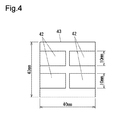
- the laminated body is set in the vacuum deposition apparatus, and hole transport layer 8 is formed on the electrode 1 with using the mask 43 having the opening 42 shown in Fig. 4 .
- the deposition is performed under a condition of reduced pressure of 5 ⁇ 10 -5 Pa.
- the hole transport layer 8 is made of 4,4'-bis[N-(naphthyl)-N-phenyl-amino]biphenyl ([alpha]-NPD).
- the hole transport layer 8 has a thickness of 40 nm.
- the light emission layer 3 having the thickness of 30 nm made of Alq3 doped with 6 percent by mass of rubrene was prepared on the hole transport layer 8 .
- the charge transport layer 9 which is made of TpPyPhB shown in the following chemical formula 1 and which has a thickness of 65 nm is formed.
- the mask 43 was changed for the mask 44 which has a size shown in Fig. 5 , and which has an opening 45 .
- the charge injection layer and the cathode is formed; the charge injection layer is made of LiF and has a thickness of 1 nm; the cathode acts as the light reflective electrode 2 and is made of Al to have a thickness of 80 nm. Consequently, the organic electroluminescence element is obtained.
- the organic electroluminescence element was prepared according to same condition of example 1 , except for the thickness of the charge transport layer 9 ; the thickness of the charge transport layer is 155 nm.
- the organic electroluminescence element was prepared according to the same condition of the example 1 , except for the thickness of the charge transport layer 9 ; the thickness of the charge transport layer 9 is 235 nm.
- the organic electroluminescence element was prepared according to the same condition of example 1, except for the thickness of the charge transport layer 9 ; the thickness of the charge transport layer 9 has a thickness of 350 nm.
- the organic electroluminescence element was prepared according to the same condition of the example 1 , except for the thickness of the charge transport layer 9 ; the thickness of the charge transport layer 9 was 435 nm.
- the region 7 , the electrode 1 , the hole transport layer 8 , the light emission layer 3 (in other words, first light emission layer 3) were formed in order and were formed on the substrate 6 .
- the charge transport layer 9 which is made of TpPyPhB and which has a thickness of 50 nm is formed.
- the charge supply layer 10 a certain layer and molybdenum oxide layer were formed.
- the certain layer is made of TmPyPhB doped with Li such that the mole ratio of TmPyPhB : Li is equal to 1 : 0,3.
- the certain layer has a thickness of 10 nm.
- the molybdenum oxide layer has a thickness of 10 nm.
- the hole transport layer 8 , the second light emission layer 3 , and the charge transport layer 9 were fromed; the hole transport layer 8 is made of alpha-NPD and has a thickness of 110 nm; the second light emission layer 3 is made of TBADN shown in the following chemical formula 3 doped with TBP shown in the following chemical formula 4 to have a thickness of 30 nm; the charge transport layer 9 was made of TpPyPhB and had a thickness of 50 nm. Furthermore, the charge injection layer and the cathode were formed; the charge injection layer was made of LiF and had a thickness of 1 nm; the cathode was made of Al and had a thickness of 80 nm. Consequently, the organic electroluminescence element having two light emission layers 3 was prepared.
- the region 7 , the electrode 1 , the hole transport layer 8 , the light emission layer 3 , the charge transport layer 9 , the charge supply layer 10 , and the molybdenum oxide layer were formed on the substrate 6 in order, under the same condition of the example 4 .
- the hole transport layer 8 which was made of alpha-NPD and which had a thickness of 200 nm was formed.
- the second light emission layer 3 is formed, and subsequently the charge transport layer 9 made of TpPhPhB and having a thickness of 150 nm was formed.
- the charge injection layer and the cathode were formed, whereby the organic electroluminescence element having two light emission layers 3 was prepared.
- the organic electroluminescence element was prepared under the same condition of the example 1 , except for the charge transport layer 9 ; the charge transport layer 9 was made of TmPyPhB and had a thickness of 70 nm.
- the organic electroluminescence element was prepared according to the same condition of the example 1 , except for the charge transport layer 9 ; the charge transport layer 9 was made of TmPyPhB and had a thickness of 170 nm.
- the organic electroluminescence element was prepared according to the same condition of the example 1 , except for the charge transport layer 9 ; the charge transport layer 9 was made of TmPyPhB and had a thickness of 230 nm.
- the organic electroluminescence element was prepared according to the same condition of the example 1 , except for the charge transport layer 9 ; the charge transport layer 9 was made of TmPyPhB and had a thickness of 345 nm.
- the organic electroluminescence element was prepared according to the same condition of the example 1 , except for the charge transport layer 9 ; the charge transport layer 9 was made of DPB and had a thickness of 85 nm.
- the organic electroluminescence element was prepared according to the same condition of the example 1 , except for the charge transport layer 9 ; the charge transport layer 9 was made of DPB and had a thickness of 185 nm.
- the organic electroluminescence element was prepared according to the same condition of the example 1 , except for the charge transport layer 9 ; the charge transport layer 9 was made of DPB and had a thickness of 275 nm.
- the organic electroluminescence element was prepared according to the same condition of the example 1 , except for the charge transport layer 9 ; the charge transport layer 9 was made of DPB and had a thickness of 380 nm. (The photoluminescence spectrum of the luminescent material of the light emission layer 3 )
- the co-deposited film was prepared on the glass substrate; the co-deposited film comprises Alq3 as a host and rubrene as a light emission dopant; the Alq3 is doped with the rubrene of 6 percent by mass. According to the measurement of the photoluminescence spectrum, the photoluminescence spectrum has a maximum value when the wavelength is equal to 559 nm.
- the product obtained by multiplying the spectral radiant flux and the CIE standard relative luminosity factor has a maximum value when the wavelength " ⁇ 1 (lambda 1 )" is 559 nm.
- the quotient obtained by dividing the spectral radiant flux and the photon energy in each the wavelength has a maximum value when the wavelength " ⁇ 2 (lambda 2 )" is 561 nm.
- the co-deposited film was prepared on the glass substrate; the co-deposited film comprises the host and the light emission dopant; the co-deposited film was a TBADN doped with 4 percent by mass of the TBP Then, the photoluminescence spectrum was measured in the same fashion of rubrene. In this case, the photoluminescence spectrum has a maximum value when the wavelength " ⁇ 1 (lambda 1 )" was equal to 462 nm.
- the product obtained by multiplying the spectral radiant flux and CIE standard luminosity factor has a maximum value when the wavelength " ⁇ 1 (lambda 1 )" is equal to 504 nm.
- the quotient obtained by dividing the spectral radiant flux by the photon energy in each the wavelength has maximum value when the wavelength " ⁇ 2 (lambda 2 )" is equal to 464 nm.
- the refractive index and the extinction coefficient of each the wavelengths " ⁇ 1 (lambda 1 )" and “ ⁇ 2 (lambda 2 )" of rubrene and TBP are shown in the following table.
- the wavelengths “ ⁇ 1 (lambda 1 )” and “ ⁇ 2 (lambda 2 )” of the rubrene are shown in Table 1.
- the wavelengths “ ⁇ 1 (lambda 1 )" and “ ⁇ 2 (lambda 2 )" of the TBP are shown in Table 2.
- the following table shows the values of the refractive index "n” and the extinction coefficience "k” with regard to the TpPyPhB which is used as the charge transport material.
- the following table shows the values of the refractive index "n”.
- Alq3 is doped with 6 percent by mass of rubrene as the dopant.
- TBADN is doped with 4 percent by mass of TBP as the dopant.
- these dopants have a little amount with respect to the Alq3 and the TBADN.
- the optical property of each the layers are substituted by the optical property of the layers of single Alq3 and single TBADN.
- the refractive index of the layer employed as the charge supply layer comprising TpPhPyB doped with Li is considered to be equal to the refractive index of the layer of single TpPyPhB.
- the current efficiency of the light flux (lm/A) is calculated; the current efficiency of the light flux is shown in the Table 3 .
- Table 3 shows the optical distance "nd" between the luminous point and the light reflective electrode 2 , the wavelength “ ⁇ 1 (lambda 1 )", the phase shift ⁇ in the wavelength " ⁇ 1 (lambda 1 )", the value a which is calculated on the basis of the formula ( 1 ) with the optical distance "nd” and the phase shift ⁇ , and the range of a which satisfies the formula ( 1 ) are also shown.
- the portion where the light emission layer 3 is in contact with the hole transport layer 8 is defined as the luminous point.
- the optical distance "nd" is represented by the sum of the product obtained by multiplying the refractive index of the light emission layer 3 and the thickness of the light emission layer 3 and the product obtained by multiplying the refractive index of the charge transport layer 9 and the thickness of the charge transport layer 9 .
- the table 4 shows the result of the quantum efficacy of the light which is in proportion with the photon number, on the basis of the calculating result.
- Table 4 shows the optical distance "nd" between the luminous point and the light reflective electrode 2 , the wavelength “ ⁇ 1 (lambda 1 )", the phase shift ⁇ in the wavelength "" ⁇ 1 (lambda 1 )", the value a which is calculated on the basis of the formula ( 2 ) with the optical distance "nd” and the phase shift ⁇ , and the range of a which satisfies the formula ( 2 ) are also shown.
- the portion where the light emission layer 3 is in contact with the hole transport layer 8 is defined as the luminous point.
- the optical distance "nd" is represented by the sum of the product obtained by multiplying the refractive index of the light emission layer 3 and the thickness of the light emission layer 3 and the product obtained by multiplying the refractive index of the charge transport layer 9 and the thickness of the charge transport layer 9 .
Landscapes
- Physics & Mathematics (AREA)
- Optics & Photonics (AREA)
- Electroluminescent Light Sources (AREA)
Abstract

A is a wavelength of the light from the light emission layer. N is a refrective index of a certain layer between the luminous point and the light-reflective-electrode at A. n1 and k1 is a refractive index and the extinction coefficience of the certain layer at A. n2 and k2 is a refractive index and the extinction coefficience of the light-reflective-electrode at A. m is 0 or 1. When "m" is 0, "a" satisfies the following formula.

When "m" is 1, "a" satisfies the following formula.

norg is a refractive index of a predetermined layer in contact with the light emission layer to be located on the same side as the light-reflective-electrode at A. nEML is a refractive index of the light emission layer at A.
Description
- This invention relates to organic electroluminescence elements which are used for a lighting source, a backlight for the liquid crystal display instrument, and a flat panel display. Specifically, this invention relates to the organic electroluminescence elements which are designed on the basis of the adequate optical design to have a good light emitting property when the light scattering region is provided on the outer surface of the light transmissive substrate, which is defined as a part of the organic electroluminescence element.
-
Fig. 6 shows one example of the structure of the organic electroluminescence element. The organic electroluminescence element comprises a lighttransmissive substrate 6, a lighttransmissive electrode 1 which is defined as an anode, ahole transport layer 8, alight emission layer 3, anelectron transport layer 9, and a lightreflective electrode 2 defined as a cathode. The lighttransmissive electrode 1, thehole transport layer 8, thelight emission layer 3, theelectron transport layer 9, a lightreflective electrode 2 are provided on the upper surface of the lighttransmissive substrate 6 such that the lighttransmissive electrode 1, thehole transport layer 8, thelight emission layer 3, theelectron transport layer 9, a lightreflective electrode 2 are arranged in order. In this organic electroluminescence element, when the voltage is applied between theelectrode 1 and theelectrode 2, the electron is injected into thelight emission layer 3 through theelectron transport layer 9. Similarly, when the voltage is applied between theelectrode 1 and theelectrode 2, the hole is injected into the light emission layer through thehole transport layer 8. When the electron is recombined with the hole in thelight emission layer 3, the light emission is made in thelight emission layer 3. The light emitted in thelight emission layer 3 is sent to the outside through the lighttransmissive electrode 1 and the lighttransmissive substrate 6. - Such the organic electroluminescence element has a property of emitting the light by itself. In addition, the organic electroluminescence element has a light emission property of comparatively high efficiency. In addition, the organic electroluminescence element has a property of emitting the light having various colors. The organic electroluminescence element is expected to be used for the luminous body for the display device such as flat panel display, a light source such as a backlight of the liquid crystal display, and a lighting device. In addition, a part of the organic electroluminescence element is practically used.
- However, the organic electroluminescence element is a thin film device having a thickness which is approximately same as an order of the optical wavelength. In addition, the organic electroluminescence element has the thickness which is correlated with the light emission property. Thus, there is a necessity for the device structure of the electroluminescence element to have the design of the film design which is suitable for both the electrical design and the optical design.
- In general, when the organic electroluminescence element generates the light in the
light emission layer 3 of the organic electroluminescence, the light is totally reflected by thelight emission layer 3, theorganic layer 4, inside of the electrode, and the inside of thesubstrate 6, whereby the light generated in the organic electroluminescence element is confined in thelight emission layer 3, theorganic layer 4, inside of the electrode, and the inside of thesubstrate 6. According to a simple estimation, when thelight emission layer 3 generates the light, 50 percents of the light generated in thelight emission layer 3 is confined in the inside oflight emission layer 3, the inside of theorganic layer 4, and the inside of the lighttransparent electrode 1. In addition, 30 percents of the light generated in thelight emission layer 3 is confined in the inside of thesubstrate 6. Therefore, the an amount of the light which is emitted to the outside is only 20 percents of the total amount. - In addition, as shown in
Fig. 7 , it is well known for thesubstrate 6 that thelight scattering region 7 is disposed on the outer surface of thesubstrate 6. Thelight scattering region 7 allows a part of the light confined in thesubstrate 6 to be extracted to the outside of the organic electroluminescence element. This configuration makes it possible to increase an amount of the light which is extracted to the outside of the organic electroluminescence element. - In addition, as shown in
Fig. 1 , it is well known to employ the lighttransmissive electrode 1 and thesubstrate 6 with alight scattering region 7 between the lighttransmissive electrode 1 and thesubstrate 6. In this case, a part of the light which is confined in thelight emission layer 3, theorganic layer 4, and the lighttransmissive electrode 1 is extracted from the organic electroluminescence element. As mentioned above, an amount of the light which is confined in thelight emission layer 3, theorganic layer 4, and the lighttransmissive electrode 1 is greater than an amount of the light which is confined in thesubstrate 6. Therefore, the organic electroluminescence element comprises the lighttransmissive electrode 1 and thesubstrate 6 with thelight scattering region 7 between the lighttransmissive electrode 1 and thesubstrate 6 is configured to emit the light having an amount which is greater than an amount of the light which is emitted from the organic electroluminescence element comprising thesubstrate 6 with thelight scattering region 7 on the outer surface of thesubstrate 6. - In addition, in such the organic electroluminescence element, there are some reports of the organic electroluminescence element having a designing of the distance between the luminous point in the
light emission layer 3 and the lighttransmissive electrode 2 in order to increase an amount of the light which is given off to the outside of the organic electroluminescence element. For example, the organic electroluminescence element disclosed in thepatent literature 1 has a luminous point and the lighttransmissive electrode 1 to create a distance between the luminous point and the lighttransmissive electrode 1; the distance between the luminous point and the lighttransmissive electrode 1 is approximately equal to an even multiple of the one-quarter of the wavelength. In addition, the organic electroluminescence element has the luminous point and the lightreflective electrode 2 to create a distance which is approximately equal to an odd multiple of one-quarter of the wavelength. Thepatent literature 2 discloses the electroluminescence element comprising the electrodes which are arranged to create the distance between the electrodes; the distance is determined on the basis of the phase shift of the light. Thepatent literature 3 disclose the organic electroluminescence element comprising the lighttransmissive electrode 1 and the lightreflective electrode 2 which are arranged to create the distance between the lighttransmissive electrode 1 and the light reflective electrode; the distance is set within a predetermined range which is determined on the basis of the phase shift of the light in the lightreflective electrode 2. In addition, each one of thepatent literature 4 and thepatent literature 5 discloses the organic electroluminescence element which comprises thesubstrate 6 with thelight scattering region 7, and the electrodes which are arranged to create the distance between the electrodes; the distance between the electrodes are determined to have a predetermined value. - Each one of the patent literatures discloses that the organic electroluminescence element has the luminescence efficiency which is greatly related to the thickness of the light transparent film which constitutes the organic electroluminescence element. In addition, each the patent literature discloses to employ the luminous point and the light
reflective electrode 2 with "the film having a particular optical thickness" between the luminous point and the lightreflective electrode 2 in order to obtain the good efficiency under a condition where the particular optical thickness satisfies the following exemplified formula. "The particular optical thickness is equal to (2m+1)/4 multiple of the luminous wavelength (m is an integer number and is more than zero). - However, the
patent literature 1 fails to disclose the consideration of the phase shift of the light in the lightreflective electrode 2. In addition, thepatent literature 2 discloses the target spectrum; the half width of the spectrum is limited to be equal to or less than 50 nanometers. Thepatent literature 3 only defines the distance between the electrodes. In contrast, thepatent literature 3 discloses no definition of the distance between the luminous point and the lightreflective electrode 2. Furthermore, each one of thepatent literatures 1 to 3 discloses the optical designing of the organic electroluminescence element which employs the substrate and other members without light scatteringregion 7 on the substrate and other members. - In contrast, each one of the
patent literatures light scattering region 7. However, each one of thepatent literatures light emission layer 3 and the lightreflective electrode 2 to create the distance of a certain level between thelight emission layer 3 and the lightreflective electrode 2. This is similar to thepatent literature 2. - In view of this, the applicant of this application discloses the appropriate distance between the luminous point and the light
reflective electrode 2 in a case where thelight scattering region 7 is disposed on the outer surface of thesubstrate 6 shown inFig. 7 and where there is a need to create the distance between thelight emission layer 3 and the lightreflective electrode 2, with respect to arbitral luminescence spectrum. - However, as will be understood from the previous explanation, the organic electroluminescence element comprising the
light scattering region 7 between the lighttransmissive electrode 3 and thesubstrate 6 emits the light which has an amount which is greater than an amount of the organic electroluminescence element comprising alight scattering region 7 on the outer surface of thesubstrate 6. With regard to the organic electroluminescence element having this configuration, a design principle of the suitable distance between the luminous point and the lightreflective electrode 2 under a situation where a certain distance is needed between thelight emission layer 3 and the lightreflective electrode 2 with respect to the arbitral emission spectrum is not cleared. - In addition, recently, an organic electroluminescence element of new type shown in
Fig. 2 is disclosed. This organic electroluminescence element comprises a plurality of thelight emission layers 3 and acharge supply layer 10 which is disposed between thelight emission layers 3; thecharge supply layer 10 comprises a light transmissive electrode, and a charge generation layer which comprises layers such as a an organic semiconductor, an inorganic semiconductor, an electron accepting material, and an electron releasing material. A plurality of thelight emission layer 3 are stacked along a thickness direction of the organic electroluminescence element. The organic electroluminescence element of the above type has a possibility of emitting the light having a high brightness, and of long operating life, whereby the organic electroluminescence element of the above type is highly expected its future progress. However, the principle of the optical design for the future progress is not clear yet. Furthermore, there is no report of the configuration of providing "a region for reflecting the light and disturbing the angle of thelight 7" between the lighttransmissive electrode 1 and thesubstrate 6. -
Patent literature 1
Japanese patent application publication No.2000-243573 -
Patent literature 2
Japanese patent application publication No.2004-165154 -
Patent literature 3
Japanese patent application publication No.2006-253015 -
Patent literature 4
Japanese patent application publication No.2004-296423 -
Patent literature 5
Japanese patent application publication No.2004-296429 - This invention is achieved in view of the above matter. An object in this invention is to produce an organic electroluminescence element having a good light emitting property. The organic electroluminescence element is produced on the basis of the adequate optical designing, whereby the organic electroluminescence element comprises a light transmissive electrode, a light transmissive substrate, and a light scattering region which is located in a position between the light transmissive electrode and the light transmissive substrate; the position of the light scattering region is determined on the basis of the adequate optical designing.
- In order to solve the above problem, the organic electroluminescence element in this invention comprises a light transmissive electrode, a light reflective electrode, an organic light emission layer, a light scattering layer, and a light transmissive substrate. The organic light emission layer comprises a light emission layer which comprises a a luminescent material. The organic light emission layer has a first surface and a second surface which is opposite of the first surface from the organic light emission layer. The light reflective electrode is disposed on the first surface. The light transmissive electrode is disposed on the second surface. The light scattering layer is disposed on the light transmissive electrode. The light transmissive substrate is disposed on the light scattering layer. The light reflective electrode is separated from the luminous point of the light emission layer by "d". The "d" satisfies the following formula.


When "m" is equal to 1, "a" satisfies a following formula
- "norg" is a refractive index of a layer which is in contact with the light emission layer and which is located on a same side of the light emission layer as the light reflective electrode at the light having the wavelength "A",
- "nEML" is a refractive index of the light emission layer at the light having the wavelength "λ".
- It is preferred that the wavelength λ of a predetermined light satisfies a condition where a product being obtained by multiplying a spectral radiant flux of the photoluminescence spectrum of the predetermined light and the CIE standard luminosity factor has maximum.
- In this case, it is possible to increase the light flux which is emitted from the organic electroluminescence element.
- It is preferred that the wavelength λ satisfies a condition where a quotient which is obtained by dividing the spectral radiant flux of the photoluminescence spectrum of a predetermined light by a photon energy of each the energy has a maximum.
- In this case, it is possible to increase the photon number which is emitted from the organic electroluminescence element.
- It is preferred that the organic light emission layer has two light emission layers. In this case, the distance between the luminous point of each the light emission layer and the first electrode is defined by "d".
- In this case, it is possible to especially increase the light flux or the photon number which are emitted from the organic electroluminescence element.
-
-
Fig. 1 shows a schematic cross sectional view of one example of the organic electroluminescence element. -
Fig. 2 shows a schematic cross sectional view of another example of the organic electroluminescence element. -
Fig. 3 shows a planar view of the glass substrate used in the example; the glass substrate is provided with ITO after the etching treatment. -
Fig. 4 shows a planar view of a mask which is used in the example; the mask is provided for forming the hole transport layer, the light emission layer, and the charge transport layer -
Fig. 5 shows a planar view of the mask which is used in the example; the mask is provided for forming the electron injection layer and the light reflective electrode. -
Fig. 6 shows a schematic side cross sectional view of one prior technique. -
Fig. 7 shows a schematic side cross sectional view of another prior technique. - Hereinafter, explanation of the best mode for carrying out the invention is made.
-
Fig. 1 shows one example of a configuration of the organic electroluminescence element. The organic electroluminescence element comprises alight transmissive substrate 6, alight scattering layer 7, alight transmissive electrode 1, an organiclight emission layer 5, and a lightreflective electrode 2. Thelight scattering layer 7 is disposed on thelight transmissive substrate 6. Thelight transmissive electrode 1 is disposed on thelight scattering layer 7. The organiclight emission layer 5 is disposed on thelight transmissive electrode 1. The lightreflective electrode 2 is disposed on the organiclight emission layer 5. Therefore, the lightreflective electrode 2 is disposed on the lower surface of the organiclight emission layer 5. (The lightreflective electrode 2 is disposed on the first surface of the organiclight emission layer 5.) Thelight transmissive electrode 1 is disposed on the upper surface of the organiclight emission layer 5. (Thelight transmissive electrode 1 id disposed on the second surface of the organiclight emission layer 5.) In addition, thelight scattering layer 7, thelight transmissive electrode 1, the organiclight emission layer 5, and the lightreflective electrode 2 are stacked on thelight transmissive substrate 6 such that thelight scattering layer 7, thelight transmissive electrode 1, the organiclight emission layer 5, and the lightreflective electrode 2 are arranged in order. The organiclight emission layer 5 comprises alight emission layer 3 which is made of luminescence material. Further, in addition to thelight emission layer 3, the organic light emission layer comprises anorganic layer 4 arbitrarily; theorganic layer 4 is exemplified by a charge injection layer, thecharge transport layer 9, the hole blocking layer, the hole injection layer, thehole transport layer 8 which are stacked. In the example shown in the illustration, thecharge transport layer 9 is interposed between the lightreflective electrode 2 and thelight emission layer 3. Thehole transport layer 8 is interposed between the light transmissive electrode and thelight emission layer 3. It is noted that a plurality of thelight emission layer 3 on the light emission layer may be employed as the light emission layer which is explained in the above. In addition, when the organiclight emission layer 5 receives the voltage, the light emission layer emits the light. - The light
reflective electrode 2 is configured to reflect the light which is emitted from the organiclight emission layer 5. In contrast, thelight transmissive electrode 1 is configured to transmit the light which is emitted from thelight emission layer 5. In addition, thelight transmissive electrode 1 is configured to transmit the light which is firstly emitted from the organiclight emission layer 5 and is then reflected by the lightreflective electrode 2. The light which is transmitted through thelight transmissive electrode 1 is scattered by thelight scattering layer 7. Thelight transmissive substrate 6 is configured to transmit the light which is scattered by thelight scattering layer 7. In this manner, the organic electroluminescence element emits the light. - In addition,
Fig. 2 shows one example of the electroluminescence element which comprises twolight emission layer 3, In the illustrated example, thelight scattering layer 7 is disposed on thelight transmissive substrate 6. Thelight transmissive electrode 1 is disposed on thelight scattering layer 7. A first organiclight emission layer 5 is disposed on thelight transmissive electrode 1. Thecharge supply layer 10 is disposed on the first organic light emission layer. A second organiclight emission layer 5 is disposed on thecharge supply layer 10. The lightreflective electrode 2 is disposed on the second organiclight emission layer 5. Therefore, thelight scattering layer 7, thelight transmissive electrode 1, the first organiclight emission layer 5, thecharge supplying layer 10, the second organiclight emission layer 5, and the lightreflective electrode 2 are stacked on thelight transmissive substrate 6 such that thelight scattering layer 7, thelight transmissive electrode 1, the first organiclight emission layer 5, thecharge supply layer 10, the second organiclight emission layer 5, and the lightreflective electrode 2 are arranged in series. Similar to the above explanation, each one of the organiclight emission layer 5 comprises thelight emission layer 3 which includes the luminescence material. Further, in addition to thelight emission layer 3, each one of the organiclight emission layer 5 comprises theorganic layer 4, arbitrarily; theorganic layer 4 comprises the charge injection layer, thecharge transport layer 9, the hole blocking layer, the hole injection layer, and thehole transport layer 8. Therefore, the organic electroluminescence element shown inFig. 2 may be considered to have one organic light emission layer comprising a plurality of the light emission layers. In the illustrated example, the lightreflective electrode 2 is located on a same side of the organiclight emission layer 5 as thecharge transport layer 9. Thehole transport layer 8 is disposed on the same side of the organiclight emission layer 5 as thelight transmissive electrode 1. - In addition, the organic electroluminescence element may comprises a plurality of the light emission layers 3. In this case, a plurality of the
charge supply layer 10 is interposed between thelight transmissive electrode 1 and the lightreflective electrode 2. In addition, the organiclight emission layer 5 is interposed between thelight transmissive electrode 1 and thecharge supply layer 10. In addition, the organic light emission layer is interposed between thecharge supply layer 10 and the lightreflective electrode 2. The organic electroluminescence elements are constituted according to the above. In addition, it is possible to stack a plurality of the light emission layers in the organiclight emission layer 5. When a plurality of thelight emission layers 3 are employed, the number of the stacked layer is not limited. However, increase of the number of thelight emission layer 3 causes the increase of the difficulty of the optical designing and the electrical designing of the organic electroluminescence element. Therefore, it is preferred that the number of thelight emission layers 3 is equal to or less than five. In addition, it is more preferred that the number of the light emission layers is equal to or less than three. - In the organic electroluminescence element, the
light scattering layer 7 is only required to have a property of effectively varying the light transmission angle more than totally reflecting angle into the light transmission angle less than totally reflecting angle. Thelight scattering layer 7 having the above property makes it possible for the organic electroluminescence element to emit the light which travels inside the organic electroluminescence element is emitted to the outside of the organic electroluminescence element. Such thelight scattering layer 7 is realized by the layer which is provided at its surface with irregularity. In addition, thelight scattering layer 7 comprises a layer having a boundary which has a light reflective property. In addition, thelight scattering layer 7 may be realized by a layer which comprises medium which are different in the refractive index from each other and which are in contact with each other to make boundaries. "The layer comprising particles or voids" and "the layer made of a plurality of the materials which are mixed with each other" act as thelight scattering layer 7. The light scattering layer is disposed on thesubstrate 6. In addition, it is possible to employ the substrate which is provided at its surface with the irregularity. In this case, the surface with irregularity of the substrate is defined as thelight scattering layer 7. Furthermore, it is possible to employ arbitral configuration as thelight scattering layer 7 unless the arbitral configurations are against the spirit of the invention. For example, it is possible to form thelight scattering layer 7 by a scattering particle layer which is realized by the transparent material with the particles or voids; the transparent material is exemplified by the polyester series resin, the epoxy resin, the polyurethane series resin, the silicone series resin, and the acrylic series resin; the particles are exemplified by silica particles, titania particles, zirconia particles, plastic particles, and the liquid crystal particles which respectively have refractive index which is different from the refractive index of the transparent material. In addition, it is possible to form the planarizing layer on the scattering particle layer. In this case, the planarizing layer is made of transparent resin. The scattering particle layer is cooperative with the planarizing layer to constitute thelight scattering layer 7. The transparent resin for forming the planarizing layer may include fine particles which has sizes smaller than the sized of the particles in the scattering layer, if needed. The planarizing layer is provided for flatting thelight scattering layer 7 in order to flatting the light transmissive electrode under a condition where thelight transmissive electrode 1 is stacked on thelight scattering layer 7. It is preferred to employ the planarizing layer which is made of material having the refractive index which is approximately equal to the refractive index of thelight transmissive electrode 1. "Approximately equal" means the refractive index with a margin of plus or minus 0.1. - It is preferred that the
light scattering layer 7 has a light transmission rate which is equal to or more than 50 percents. It is more preferred that thelight scattering layer 7 has a light transmission rate which is equal to or more than 80 percents. It is noted that a variation of the directionality of the light of thelight scattering layer 7 is not limited, especially. However, it is preferred to employ thelight scattering layer 7 which has a designing of not totally reflecting the light but transmitting the light. - In addition, the conventional members such as the anode, cathode, the
light emission layer 3, thecharge transport layer 9, thecharge supply layer 10 may be employed as a components which constitute the organic electroluminescence element without any modification. - The
light transmissive substrate 6 may be realized by the transparent glass plate made of material such as soda lime glass and alkali-free glass. Thelight transmissive substrate 6 also may be realized by the plastic film and the plastic plate which are made of resin such as polyester, polyolefin, polyamide, epoxy, and fluorine series and which are manufactured by the arbitrary process. - The anode is an electrode which is provided for injecting the hole into the
light emission layer 3. It is preferred for the anode electrode to be made of the electrode material such as metal, alloy, electrical conductive compound, and a mixture of the metal, alloy, and electrical conductive compound, which has a large work function. It is preferred for the anode to be made of the electrode material having the work function of more than 4rev. The material of the anode satisfying the above requirement is exemplified by Cul, ITO (indium tin oxide), SnO2 ZnO, IZO (indium zinc oxide), PEDOT, electro conductive polymer such as polyaniline electro conductive polymer with arbitral acceptor as a dopant, and electrical conductive- transparent material such as carbon nanotube. The anode is realized by thelight scattering layer 7 and a thin film on the surface of the light scattering layer7; the thin film is formed by vacuum deposition, sputtering, and application. - In addition, if the anode is realized by the
light transmissive electrode 1, it is preferred to employ thelight transmissive electrode 1 having the light transmission rate of equal to or more than 70 %. - In addition, it is preferred that the anode has a sheet resistance which is equal to or less than several hundreds ohm per square. It is more preferred that the anode has the sheet resistance which is equal to or less than one hundred ohm per square. The anode is varied its film thickness according to the material for controlling the property of the light transmission rate of the anode and the sheet resistance. However, the anode has the film thickness of equal or less than 500 nm. In addition, the anode has the film thickness of equal to or less than 10 nm and equal to or less than 200 nm.
- The cathode is an electrode for injecting the electron into the
light emission layer 3. It is preferred for the cathode to be made of the electrode material such as metal, alloy, electrical conductive compound, and the mixture thereof which have low work function. It is more preferred that the cathode has the work function of equal to or less than 5 eV. The electrode material of the cathode is exemplified by alkali metal, alkali metal halide, alkali metal oxide, alkali earths metal, and the alloy thereof with the other metals; alloys are exemplified by sodium, sodium potassium alloy, lithium, magnesium, magnesium silver mixture, magnesium indium mixture, aluminum lithium alloy, and aluminum lithium fluorine mixture. In addition, aluminum, and aluminum-aluminum oxide mixture may be used as the electrode material of the cathode. Furthermore, it is also possible to employ the cathode which comprises the foundation layer and the metal layer prepared on the foundation layer; the foundation layer is made of material such as alkali metal oxide, alkali metal halide, metal oxide; the metal layer comprises more than one layer which is made of metal. Such the cathode is exemplified by the multilayer which is exemplified by alkali metal/aluminum, alkali metal halide/ alkali earth metal/ aluminum, alkali metal oxide/aluminum. As to the alternative means of the above, it is possible to realize the lightreflective electrode 2 by the transparent electrode in combination with the light reflective layer. Furthermore, the cathode may be realized by the transparent electrode such as ITO and IZO. In this case, the cathode is prepared on thesubstrate 6. In this case, it is possible to dope alkali metal or alkali earth metal to the organic layer which is defined as a boundary of the cathode with respect to the substrate; the alkali metal and alkali earth metal are exemplified by lithium, sodium, cesium, and calcium. - In addition, the cathode is, for example, realized by the thin film which is formed by the vacuum deposition and a sputtering. If the cathode is realized by the light
reflective electrode 2, it is preferred for the lightreflective electrode 2 to have the light transmission rate which is equal to or less than 10 percents. If the cathode is realized by thelight transmissive electrode 1, it is preferred for the cathode to have the light transmission rate which is equal to or more than 70 percents. In this case, the cathode is varied its thickness according to the material in order to control the property such as the light transmission rate of the cathode. However, it is possible for the cathode to have the film thickness which is equal to or less than 500 nm. In addition, it is preferred for the cathode to have the film thickness which is equal to or more than 100 nm and is equal to or less than 200 nm. - The
charge transport layer 9 may be made of material of a group of having an electron transport property. Such the compound is exemplified by "a metallic complex" and "a compound having heterocycle"; the metallic complex is such as Alq3 which is known as the electron transport material; the compound having heterocycle is exemplified by phenanthroline derivatives, pyridine derivatives, tetrazine derivatives, and oxadiazole derivatives. However, the compound of thecharge transport layer 9 is not limited thereto. Thecharge transport layer 9 may be determined its material by the charge transport material which is arbitrary determined and which is generally known. Especially, thecharge transport layer 9 is preferably made of the material having a high charge transport property. - The
hole transport layer 8 is made of material of compound having a hole transport property. The compound having the hole transport property is exemplified by tryarylamine compounds, amine compounds which contains carbazole unit, and amine compounds which contains fluorine derivatives. The tryarylamine compounds is exemplified by "4, 4'-bis [N-(naphthyl)-N-phenyl- amino] biphenyl (α-NPD)", "N,N'-diphenyl-N,N'-bis(3-methylphenyl)-(1,1'-biphenyl)-4,4'-diamine (TPD)", "2-TNATA", "4,4',4"-Tris(N-3-methylphenyl-N- phenylamino)triphenylamine (MTDATA)", "4,4'-N,N'-dicarbazole-biphenyl", "Spiro-NPD", "Spiro-TPD", "Spiro-TAD", "TNB". However, theelectron transport layer 9 may be made of any well known hole transport material. - In addition, the light
emissive layer 3 is made of a well known appropriate material for organic electroluminescence device. The material of the lightemissive layer 3 is exemplified by anthracene, naphthalene, pyrene, tetracene, coronene, perylene, phtaloperylene, naphthaloperylene, diphenylbutadiene, tetraphenylbutadiene, coumarine, oxadiazole, bisbenzoxazoline, bisstyryl, cyclopentadiene, quinoline metal complex, tris (8-hydroxyquinolinate) aluminum complex, tris (4-methyl-8-quinolinate) aluminum complex, tris (5-phenyl-8-quinolinate) aluminum complex, aminoquinoline metal complex, benzoquinoline metal complex, tri-(p-terphenyl-4-yl)amine, 1-aryl-2,5-di(2-thienyl) pyrrole derivatives, pyrane, quinacridone, rubrene, distyrylbenzene derivatives, distyrylarylenes derivatives, distyrylamine derivatives, fluorochromes, and these derivatives. However, the material of the lightemissive layer 3 is not limited thereto. In addition, it is preferable to use the mixture of the above appropriate materials. Furthermore, the lightemissive layer 3 may be made of materials which cause light emission from spin multiplicity in addition to the above mentioned materials which cause fluorescent emission. The material causing the light emission from the spin multiplicity is exemplified by compounds having phosphorescent properties, and compounds containing in one part of the compound having the phosphorescent property. In addition, theorganic layer 4 is formed by a dry process of a deposition, a dry transfer printing, and wet process of spin coating, spray coating, die coating, and gravure printing. - The
charge supply layer 10 is formed by a metal thin film, a metal oxide, a light transmissive electrical conductive film, a laminated film, and mixture thereof. The metal thin film made of a material is exemplified by Ag, Au, and Al, The metal oxide is exemplified by vanadium oxide, molybdenum oxide, rhenium oxide, and tungsten oxide. The light transmissive electrical conductive film is exemplified by ITO, IZO, AZO, GZO, ATO, and SnO2 The laminated film is exemplified by films of n-type impurity semiconductor and a p-type impurity semiconductor. In addition, the laminated film is exemplified by films of at least one of an n-type impurity semiconductor and a p-type impurity semiconductor and at least one of a metal thin film and a light transmissive film. The mixture is exemplified by a mixture of n-type impurity semiconductor and the p-type impurity semiconductor, and a mixture of n-type impurity semiconductor and/or the p-type impurity semiconductor and the metal. Both the n-type impurity semiconductor and the p-type impurity semiconductor may be made of an organic material or an inorganic material. In addition, both the n-type impurity semiconductor and the p-type impurity semiconductor may be made of a mixture of the organic material and the metal, a mixture of the organic material and the metal oxide, a mixture of an organic material and an organic donor/accepter material, and a mixture of the organic material and an inorganic donorlaccepter material. That is, the material of thecharge supply layer 10 is not limited thereto, and is determined as necessary. - The organic electroluminescence element comprises the organic
light emission layer 5 including thelight emission layer 3 is interposed between thelight transmissive electrode 1 and the lightreflective electrode 2. Thelight scattering layer 7 is disposed on thelight transmissive electrode 1. Thelight transmissive substrate 6 is disposed on thelight scattering layer 7. The organic electroluminescence element has a designing for increasing the light flux or photon number. - First, an explanation of increasing the light flux emitted from the organic electroluminescence element is made. The organic electroluminescence element is designed such that the luminous point of at least one of the
light emission layer 3 of the organiclight emission layer 5 is separated from the lightreflective electrode 2 by a distance "d" which satisfies the following formula (1). This configuration makes it possible to increase the light flux emitted from the organic electroluminescence element which comprises thelight scattering layer 7. - It is noted that the luminous point is defined by a position where luminescence intensity of the light has maximum in the thickness direction of the
light emission layer 3. It is difficult to determine the position of the luminous point by way of experiment, directly. However, it is possible to estimate the position of the luminous point by the optical calculation on the basis of the method of the film thickness dependence of the luminescence spectrum. Furthermore, it is also possible to determine the luminous point from the experience which is based on "the carrier mobility and the energy level" of theorganic layer 3 such as thelight emission layer 3, thehole transport layer 8, and thecharge transport layer 9. In addition, there is a case that the light emission portions are distributed within thelight emission layer 3 in the thickness direction. In this case, it is possible to consider the representative point having the maximum luminescence intensity as the luminous point.
"λ1" of formula (1) is a wavelength which satisfies a condition where a product obtained by multiplying "a spectral radiant flux of a photoluminescence spectrum of a predetermined light" and "a CIE relative luminosity factor" has a maximum value. That is, the formula (1) is provided for developing the condition of "increasing the light flux which is emitted from the organic electroluminescence element" on the basis of the wavelength which affects the light flux which is emitted from the organic electroluminescence element. - In addition, ϕ in the formula (1) is a phase shift of the light. The phase shift of the light is caused when the light is reflected by the region between a certain layer and the light
reflective electrode 2; the certain layer is created by a layer between the luminous point and the lightreflective electrode 2; the certain layer is in contact with the light reflective electrode. ϕ is represented by the following formula.
"n1" is a refractive index of "the layer which is located between the luminous point and the lightreflective electrode 2 and which is in contact with the lightreflective electrode 2" with respect to the light having the wavelength "λ1(lambda 1)". "k1" is an extinction coefficient "the layer which is located between the luminous point and the lightreflective electrode 2 and which is in contact with the lightreflective electrode 2" with regard to the light having the wavelength "λ1 (lambda 1)". "n2" is a refractive index of the lightreflective electrode 2 with respect to the light having the wavelength "λ1 (lambda 1)". "k2" is an extinction coefficient of the lightreflective electrode 2 with respect to the light having the wavelength "A1 (lambda 1)". - "n" in the formula (1) is a refractive index of "the film which is located between the luminous point and the light
reflective electrode 2" with respect to the light having the wavelength "λ1 (lambda 1)". "nd" is an optical distance from the luminous point to the lightreflective electrode 2 with respect to the light having the wavelength "λ1 (lambda 1)". In a case where there are a plurality of the films between the luminous point and the lightreflective electrode 2, "nd" is calculated on the basis of the following formula by use of thickness of each the films and of the refractive index of the films.
"na", "nb", ... mean the refractive indexes of the each one of the layers which are located between the luminous point and the lightreflective electrode 2. "da", "db", ... mean the thicknesses of each one of the layers which is located between the luminous point and the lightreflective electrode 2. The combination of a plurality of "da" and "db" are arbitrarily determined to satisfy the formula (1). - In addition, "m" in the formula (1) is equal to 0 or 1.
"a" is a number which satisfies the following formula when "m" is equal to 0.
"a" is a number which satisfies the following formula when "m" is equal to 1.
"norm" is a refractive index of "the layer which is located on the same side of thelight emission layer 3 as the lightreflective electrode 2 and which is in contact with thelight emission layer 3" with respect to the light having the wavelength "λ1". "nEML" is a refractive index of thelight emission layer 3 with respect to the light having the wavelength "λ1 (lambda 1)", "a" is determined its range for satisfying the condition where the value of the light flux has maximum or has near maximum by the analysis on the basis of the actual measured value. - The photoluminescence spectrum of the
light emission layer 3 is measured according to the following method, for example. Firstly, a step of preparing thin film on thesubstrate 6 is performed; the thin film is made of material of host and dopant which are mixed at a mixture ratio which is equal to the mixture ratio of the host and the dopant of thelight emission layer 3. Secondly, a step of applying the ultraviolet light to the thin film is performed. When the ultraviolet light is applied, the thin film emits the light. Thirdly, the light emitted from the thin film is measured by the integrating sphere. In this manner, the photoluminescence spectrum is measured. - In addition, the refractive index of the material which constitutes the organic electroluminescence element is measured by the device such as vertically incident type reflection and refraction meter. Furthermore, the extinction coefficient of the material which constitutes the organic electroluminescence element is measured by the device such as ellipsometer. In this case, it is possible to measure the wavelength dependency of the refractive index and the extinction coefficience in addition to the extinction coefficient.
- The thickness of the organic electroluminescence element is adjusted to the value indicated by the formula (1) on the basis of the adjustment of film thickness and the refractive index of the layer such as "the
light emission layer 3, the hole blocking layer, thecharge transport layer 9, and the charge injection layer" between thelight emission layer 3 and the lightreflective electrode 2. In addition, the organic electroluminescence element may employ a plurality of thelight emission layer 3 which is located in an inside of the charge supply layers 10. In this case, it is preferred to adjust the thickness of the layer other than thelight emission layer 3 which is closest to the light reflective electrode in order to adjust the film thickness of the organic electroluminescence element; it is preferred to adjust the thicknesses or the refractive indexes of thehole transport layer 8 adjacent to thelight emission layer 3 located near to the lightreflective electrode 2 than anotherlight emission layer 3, thehole transport layer 8, the hole injection layer, and thecharge supply layer 10. When the above adjustment is made to adjust the thickness of the organic electroluminescence element to a predetermined thickness, there is a possibility that the electrical balance in the element is lost. However, the it is possible to adjust the electrical balance in the element by varying the ratio of the film thickness of the hole injection layer and thehole transport layer 8. Similarly, it is also possible to adjust the electrical balance in the element by varying the thickness ratio ofcharge transport layer 9 with respect to the charge injection layer. In addition, it is possible to adjust the electrical balance in the element by the arbitral means of varying the material which constitutes each one of the layers, and by means of adding the additive substance for adjusting the charge transport property to each one of the layers. - In addition, the organic electroluminescence element having an inverted structure from the above organic electroluminescence element is also known; the organic electroluminescence comprises "a
light transmissive electrode 1 which acts as a cathode" and "a lightreflective electrode 2 which acts as an anode". If the organic electroluminescence element has the inverted structure from the above organic electroluminescence element, the electroluminescence element comprises thelight emission layer 3 and the light reflective electrode to have an intermediate layer therebetween; the intermediate layer is realized by thehole transport layer 8. Therefore, the organic electroluminescence element is adjusted its thickness by adjusting the thickness of thehole transport layer 8. However, it is possible to adjust the thickness of the organic electroluminescence element by the arbitrary layer, without any departure from the purpose of this invention. - In addition, if the organic electroluminescence element comprises the organic
light emission layer 5 which comprises a plurality of the light emission layers, it is required to satisfy the above formula (1) by at least one of the light emission layers 3. Consequently, an amount of the light which is emitted from the organic electroluminescence element is increased. - In addition, if the organic electroluminescence element comprises two light emission layers, it is more preferred that each one of the two light emission layers satisfies the above formula (1). In this case, the light flux which is emitted from the organic electroluminescence element is especially increased. In addition, it is preferred to dispose "one of the
light emission layers 3 which emits the light having the wavelength satisfying a predetermined condition" closer to the lightreflective electrode 2 than the other of thelight emission layer 3; the predetermined condition is a condition where the product obtained by multiplying the spectral radiant flux of the photoluminescence spectrum and the a CIE relative luminosity factor is maximum. In this case, it is possible to easily design the organic electroluminescence element to have the twolight emission layers 3 each of which satisfies the formula (1). - Next, the explanation of the configuration of increasing the number of the photon which is emitted from the organic electroluminescence element is made. In the organic electroluminescence element, the organic
light emission layer 5 and the lightreflective electrode 2 are disposed such that the luminous point of thelight emission layer 3 is separated from the lightreflective electrode 2 by a distance " d " which satisfies a following formula (2). Consequently, it is possible to increase the number of the photon which is emitted from the organic electroluminescence element which comprises thelight scattering layer 7.
"λ2 (lambda 2)" in the formula (2) is a wavelength which satisfies the condition where the quotient which is obtained by dividing spectral radiant flux of the photoluminescence spectrum of the light emitted from thelight emission layer 3 by the photon energy becomes maximum value. That is, formula (2) is a formula for obtaining "the condition of increasing the photon number of the light emitted from the organic electroluminescence element" on the basis of the wavelength which has the largest effect on the photon number of the light which is emitted from the organic electroluminescence element. - In addition, ϕ in the formula (2) is a phase shift which is occurred by the reflection of the light in the area between the light
reflective electrode 2 and a predetermined layer; the predetermined layer is located between the lightreflective electrode 2 and the luminous point of thelight emission layer 3; the predetermined layer is in contact with the lightreflective electrode 2. The phase shift is shown in the following formula
"n1" is a refractive index of a layer with respect to the wavelength "λ2 (lambda 2)"; the layer is located between the lightreflective electrode 2 and the luminous point of thelight emission layer 3; the layer is in contact with the lightreflective electrode 2. "k1" is an extinction coefficient of the wavelength "λ2" of the light in a layer; the layer is located between the lightreflective electrode 2 and the luminous point of thelight emission layer 3; the layer is in contact with the lightreflective electrode 2. "n2" is a refractive index of wavelength "λ2" of the light with respect to the lightreflective electrode 2. "k2" is an extinction coefficient of the wavelength "λ2" with respect to the lightreflective electrode 2. - In addition, "n" in the formula (2) is a refractive index of the film which is located between the luminous point and the light
reflective electrode 2, with respect to the wavelength "λ2 (lambda 2)" of the light. "nd" is an optical distance between the lightreflective electrode 2 and the luminous point with respect to the wavelength "λ2 (lambda 2)" of the light. If there are a plurality of the films which are located between the luminous point and the lightreflective electrode 2, it is possible to obtain the optical distance by the following formula, the thickness of each the layers, and the refractive index of each the layers.
- Each one of "na", "na", ... means the refractive index of each one of the layers which are located between the luminous point and the light
reflective electrode 2. Each one of "da", "db", ... means the thickness of each the layers which is located between the luminous point and the lightreflective electrode 2. Combinations of "da", "db" is determined to satisfy the above formula (2). - In addition, the formula (2) includes "m" which is equal to "0" or "1". Furthermore, "a" is a value which satisfies the following formula when "m" is equal to "0".

"a" is a value which satisfies the hollowing formula when "m" is equal to "1".
"norg" is a refractive index of a layer with respect to the wavelength "λ2 (lambda 2)" of the light; the layer is located on the same side of thelight emission layer 3 as the lightreflective electrode 2; the layer is in contact with thelight emission layer 3. "nEML" is a refractive index of thelight emission layer 3 with respect to the wavelength "λ2 (lambda 2)" of the light. A range of "a" is developed from the analysis on the basis of the actual measurement value for satisfying the condition where the number of the photon becomes maximum or approximately maximum. - The photoluminescence spectrum of the
light emission layer 3 may be measured by the following method, similar to the above method. First, the step of depositing a thin film on thesubstrate 6; the thin film is made of host and dopant at the same mixture ratio is performed. Second, the step of applying the ultraviolet light to the thin film is performed. Third, the step of measuring the light which is emitted from the thin film by the integrating sphere is performed. Consequently, the photoluminescence spectrum is measured. - In addition, the refractive index of the material which constitutes the organic electroluminescence element is measured by the device such as vertically incident type reflection and refraction meter. Furthermore, the extinction coefficient of the material which constitutes the organic electroluminescence element is measured by the device such as ellipsometer In this case, it is possible to measure the wavelength dependency of the refractive index and the extinction coefficience.
- The organic electroluminescence element is determined its thickness to have the value which is represented by the formula (2) with regulating the thicknesses and the refractive indexes of "the
light emission layer 3, the hole blocking layer, thecharge transport layer 9, the charge injection layer", which are located between thelight emission layer 3 and the lightreflective electrode 2. In addition, the organic electroluminescence element which comprises a plurality of thelight emission layers 3 which are inserted between the charge supply layers 10. In this case, it is possible to design the film thickness of the organic electroluminescence element by regulating the film thickness or the refractive index of a layer which is other than thelight emission layer 3 which is closest to the lightreflective electrode 2; the layer is, for example, thehole transport layer 8 which is adjacent to one of thelight emission layer 3 which is located closer to the lightreflective electrode 2 than the other of thelight emission layer 3, the hole injection layer, and thecharge supply layer 10; the layer. When the above adjustment is made to adjust the thickness of the organic electroluminescence element to a predetermined thickness, there is a possibility that the electrical balance in the element is lost. However, it is possible to adjust the electrical balance in the element by varying the ratio of the film thickness of the hole injection layer and thehole transport layer 8. Similarly, it is also possible to adjust the electrical balance in the element by varying the thickness ratio ofcharge transport layer 9 with respect to the charge injection layer. In addition, it is possible to adjust the electrical balance in the element by the arbitral means of varying the material which constitutes each one of the layers, and by means of adding the additive substance for adjusting the charge transport property to each one of the layers. - In addition, the organic electroluminescence element which has the inverted structure which comprises the
light transmissive electrode 1 which acts as the cathode and the lightreflective electrode 2 which acts as the anode is well known. In the organic electroluminescence element of the inverted structure, thelight emission layer 3 and the lightreflective electrode 2 are disposed to have thehole transport layer 8 therebetween. Therefore, thickness of the organic electroluminescence element is regulated according to the regulation of the film thickness of thehole transport layer 8. However, it is possible to adjust the thickness of the organic electroluminescence element by the arbitrary layer, without any departure from the purpose of this invention. - In addition, if the organic electroluminescence element comprises an organic
light emission layer 5 which comprises a plurality of the light emission layers, it is required for at least one of thelight emission layers 3 to satisfy the above formula (2). Consequently, an amount of the light which is emitted from the organic electroluminescence element is increased. - In addition, if the organic electroluminescence element comprises two light emission layers, it is preferred that each one of the two
light emission layers 3 satisfies the above formula (2). Consequently, the photon number which is emitted from the organic electroluminescence element is especially increased. In addition, it is preferred to dispose one of the light emission layer which is closer to the lightreflective electrode 2 than the other of the light emission layer; the one of the light emission layer is configured to emit the light having the wavelength which satisfies the condition where the quotient which is obtained by dividing the spectral radiant flux of the photoluminescence spectrum by the photon energy of each the wavelength. In this case, it is possible to easily design the organic electroluminescence element to have the twolight emission layer 3 which satisfy the formula (2). - In the organic electroluminescence element which has a designing of increasing the light flux or the photon number of the light which is emitted from the organic electroluminescence element, not the brightness of the light which is emitted from the organic electroluminescence element to the front but the total amount of the light which is emitted from the organic electroluminescence element is increased. Therefore, such the organic electroluminescence element is suitably employed to the device which requires an amount of the light, especially the light source, the back light, and the lighting device which requires the amount of the light.
- In addition, an amount of the light which is emitted from the
light emission layer 3 to thelight transmissive electrode 1 and also to thesubstrate 6 is increased (compared with the total amount of the light which is confined within thelight transmissive electrode 1, the light which is confined within thesubstrate 6, and the light which is emitted to the outside through thesubstrate 6 in a case where nolight scattering layer 7 is applied to the organic electroluminescence element). Therefore, it is possible to achieve the high light extracting efficiency by arranging thelight scattering layer 7 and thelight transmissive substrate 6 in this order such that thelight scattering layer 7 and thelight transmissive substrate 6 are opposite of the organiclight emission layer 5. - In addition, the organic electroluminescence element is designed to increase the total amount of the light which enters the
light transmissive electrode 1 and thesubstrate 6 from thelight emission layer 3 of the organic electroluminescence element. Therefore, even if the organic electroluminescence element comprises thelight scattering layer 7 and thelight transmissive substrate 6 which are opposite of the organic light emission layer of the light transmissive electrode in this order, and further comprises anotherlight scattering layer 7 on the outside of thelight transmissive substrate 6, it is possible to realize the high light extracting efficiency. Similarly, even if the organic electroluminescence element comprises thelight scattering layer 7 which is only disposed on the outside of thelight transmissive substrate 6, it is also possible to realize the high light extracting efficiency. - In addition, in the above organic electroluminescence element, an amount of the light is increased while the
light emission layer 3 and the lightreflective electrode 2 are disposed such that the distance between thelight emission layer 3 and the lightreflective electrode 2 is kept so as not to be too short. Therefore, the designing of the above organic electroluminescence element is preferably employed, considering the electrical short due to the film thickness. In addition, within the effect of this invention, it is possible to increase the thickness of the hole transport layer which is disposed on thelight transmissive electrode 1. In addition, it is possible to employ the hole injection layer of application type which is well known to have a property of high cover ratio with respect to the foreign matter. - According to the above, the organic electroluminescence element having the
substrate 6 provided with thelight scattering layer 7 makes it possible to realize the high light extracting efficiency, whereby it is possible to obtain the organic electroluminescence element having high efficiency. - Hereinafter, the examples are explained. However, this invention is not limited to the following examples.
- The
light transmissive substrate 6 with thelight scattering layer 7 was prepared according to the following steps. In a first, 86.8 g tetraethoxysilane was combined with 803.5 g isopropyl alcohol, and was further combined with 34.7 g gamma-methacryloxypropyl trimethoxysilane and 75 g 0.1-N nitric acid. Then, these were mixed with each other by the disper, whereby solution was obtained. The solution was agitated for 2 hours in the constant temperature reservoir of 40 degree Celsius. Consequently, 5 wt % solution of silicone resin having the weight-average molecular weight of 1050 was prepared as a binder formation material. - Then, the methyl silicone particles were added to the silicone resin solution. (The methyl silicone particles had mean diameter of 2 micrometer. The methylsilicone particles was Tospearl 120 (GE Toshiba Silicone).) The silicone resin solution has a ratio of the methyl silicone particles : the silicone resin is equal to 80 : 20 according to the solid content mass standard. (The ratio is determined on the basis of the conversion in condensation compound.) The methyl silicone particles were dispersed throughout the silicone resion solution by the homogenizer, whereby the methyl silicone particles dispersed silicone resin solution was prepared. It is noted that "the conversation in condensation compound" is a molarity of the silicone resin in a case where the hydrolytic condensation polymerization of the silicone resin is completed. When the silicone resin is a tetralkoxysilane, the molarity of the silicone resin is equal to the molarity that Si in tetralkoxysilane is calculated as SiO2. When the silicone resin is a trialkoxysilane, the molarity of the silicone resin is equal to the molarity that Si in trialkoxysilane is calculated as SiO1.5.
- The alkali free glass having the thickness of 0.7 millimeters was used as the
substrate 6. (The substrate is manufactured by Corning Co., Ltd. No. 1737). The methyl silicone particles dispersed silicone resin solution was applied to the surface of thesubstrate 6 by the spin coater under a condition where thesubstrate 6 was rotated by 1000 rpm. Then, the methyl silicone particles dispersed silicone resin solution was dried. The application and drying were performed six times. Then, the heat treatment of the film formed by the above step is performed at 200 degrees C for 30 minutes. In this manner, the light scattering layer with the particles was prepared. - Then, the imide series resin is applied on the surface of the light scattering layer with the particles by the spin coater under a condition where the light scattering layer with the particles is rotated at 2000 rpm. (The imide series resin is HRl1783 which is manufactured by OPTMATE Co., Ltd. The imide series resin has a refractive index of 1.78, and concentration of 18 percent by mass.) Then the imide series resin was dried, whereby coated film was prepared. Subsequently, the heat treatment is applied to the coated film at 200 degree C for 30 minutes. Consequently, the planarizing layer having the thickness of 4 µm was prepared. Consequently, the
substrate 6 is provided at its surface with a region which comprises the light scattering layer with the particle and the planarizing layer. - Then, the ITO film having the thickness of 150 nm was prepared on the surface of the
region 7 by the sputtering with using the target made of ITO (Indium Tin Oxide). (The target is manufactured by Tosoh Corporation.) The ITO film was annealed at 200 degree C for 1 hour under Ar atmosphere. The annealed ITO film had the sheet resistance of 18 ohm/square. - Then, the etching is performed to the ITO film, whereby the remaining portion of the ITO having the size shown in
Fig. 3 is prepared as the anode (which corresponds to the light transmissive electrode 1). Then the substrate was cut such that thesubstrate 6 was divided into regions each of which had the sizes shown inFig. 3 . Then, the ultrasonic cleaning with pure water for 10 minutes, with acetone for 10 minutes, and isopropyl alcohol for 10 minutes were performed to the laminated body which comprises thesubstrate 6, theregion 7, and theelectrode 1, in order. Subsequently, the laminated body was cleaned by isopropyl alcohol vapor for 2 minutes. After the laminated body was dried, the laminated body was further cleaned by UV ozone for 10 minutes. - The laminated body is set in the vacuum deposition apparatus, and
hole transport layer 8 is formed on theelectrode 1 with using themask 43 having the opening 42 shown inFig. 4 . The deposition is performed under a condition of reduced pressure of 5×10⁻⁵ Pa. Thehole transport layer 8 is made of 4,4'-bis[N-(naphthyl)-N-phenyl-amino]biphenyl ([alpha]-NPD). Thehole transport layer 8 has a thickness of 40 nm. Subsequently, thelight emission layer 3 having the thickness of 30 nm made of Alq3 doped with 6 percent by mass of rubrene was prepared on thehole transport layer 8. Furthermore, thecharge transport layer 9 which is made of TpPyPhB shown in the followingchemical formula 1 and which has a thickness of 65 nm is formed.

- Then, the
mask 43 was changed for themask 44 which has a size shown inFig. 5 , and which has anopening 45. Then, the charge injection layer and the cathode is formed; the charge injection layer is made of LiF and has a thickness of 1 nm; the cathode acts as the lightreflective electrode 2 and is made of Al to have a thickness of 80 nm. Consequently, the organic electroluminescence element is obtained. - The organic electroluminescence element was prepared according to same condition of example 1, except for the thickness of the
charge transport layer 9; the thickness of the charge transport layer is 155 nm. - The organic electroluminescence element was prepared according to the same condition of the example 1, except for the thickness of the
charge transport layer 9; the thickness of thecharge transport layer 9 is 235 nm. - The organic electroluminescence element was prepared according to the same condition of example 1, except for the thickness of the
charge transport layer 9; the thickness of thecharge transport layer 9 has a thickness of 350 nm. - The organic electroluminescence element was prepared according to the same condition of the example 1, except for the thickness of the
charge transport layer 9; the thickness of thecharge transport layer 9 was 435 nm. - The
region 7, theelectrode 1, thehole transport layer 8, the light emission layer 3 (in other words, first light emission layer 3) were formed in order and were formed on thesubstrate 6. Then, thecharge transport layer 9 which is made of TpPyPhB and which has a thickness of 50 nm is formed. Then, as thecharge supply layer 10, a certain layer and molybdenum oxide layer were formed. The certain layer is made of TmPyPhB doped with Li such that the mole ratio of TmPyPhB : Li is equal to 1 : 0,3. The certain layer has a thickness of 10 nm. The molybdenum oxide layer has a thickness of 10 nm. Subsequently, thehole transport layer 8, the secondlight emission layer 3, and thecharge transport layer 9 were fromed; thehole transport layer 8 is made of alpha-NPD and has a thickness of 110 nm; the secondlight emission layer 3 is made of TBADN shown in the followingchemical formula 3 doped with TBP shown in the followingchemical formula 4 to have a thickness of 30 nm; thecharge transport layer 9 was made of TpPyPhB and had a thickness of 50 nm. Furthermore, the charge injection layer and the cathode were formed; the charge injection layer was made of LiF and had a thickness of 1 nm; the cathode was made of Al and had a thickness of 80 nm. Consequently, the organic electroluminescence element having twolight emission layers 3 was prepared.

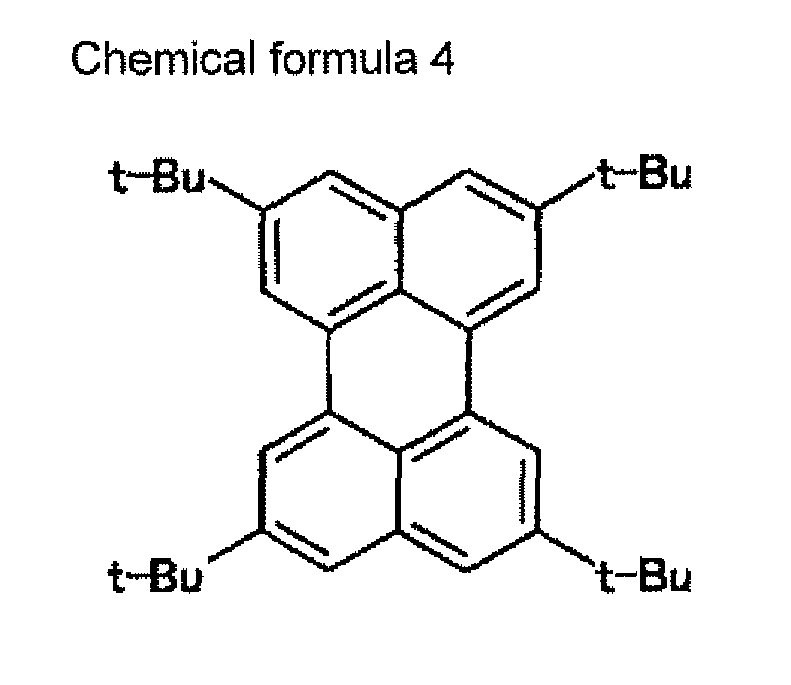
- The
region 7, theelectrode 1, thehole transport layer 8, thelight emission layer 3, thecharge transport layer 9, thecharge supply layer 10, and the molybdenum oxide layer were formed on thesubstrate 6 in order, under the same condition of the example 4. Then, thehole transport layer 8 which was made of alpha-NPD and which had a thickness of 200 nm was formed. Subsequently, according to the same condition of the example 4, the secondlight emission layer 3 is formed, and subsequently thecharge transport layer 9 made of TpPhPhB and having a thickness of 150 nm was formed. Furthermore, under the same condition of example 4, the charge injection layer and the cathode were formed, whereby the organic electroluminescence element having twolight emission layers 3 was prepared. - The organic electroluminescence element was prepared under the same condition of the example 1, except for the
charge transport layer 9; thecharge transport layer 9 was made of TmPyPhB and had a thickness of 70 nm. - The organic electroluminescence element was prepared according to the same condition of the example 1, except for the
charge transport layer 9; thecharge transport layer 9 was made of TmPyPhB and had a thickness of 170 nm. - The organic electroluminescence element was prepared according to the same condition of the example 1, except for the
charge transport layer 9; thecharge transport layer 9 was made of TmPyPhB and had a thickness of 230 nm. - The organic electroluminescence element was prepared according to the same condition of the example 1, except for the
charge transport layer 9; thecharge transport layer 9 was made of TmPyPhB and had a thickness of 345 nm. - The organic electroluminescence element was prepared according to the same condition of the example 1, except for the
charge transport layer 9; thecharge transport layer 9 was made of DPB and had a thickness of 85 nm. - The organic electroluminescence element was prepared according to the same condition of the example 1, except for the
charge transport layer 9; thecharge transport layer 9 was made of DPB and had a thickness of 185 nm. - The organic electroluminescence element was prepared according to the same condition of the example 1, except for the
charge transport layer 9; thecharge transport layer 9 was made of DPB and had a thickness of 275 nm. - The organic electroluminescence element was prepared according to the same condition of the example 1, except for the
charge transport layer 9; thecharge transport layer 9 was made of DPB and had a thickness of 380 nm.
(The photoluminescence spectrum of the luminescent material of the light emission layer 3) - The co-deposited film was prepared on the glass substrate; the co-deposited film comprises Alq3 as a host and rubrene as a light emission dopant; the Alq3 is doped with the rubrene of 6 percent by mass. According to the measurement of the photoluminescence spectrum, the photoluminescence spectrum has a maximum value when the wavelength is equal to 559 nm.
- The product obtained by multiplying the spectral radiant flux and the CIE standard relative luminosity factor has a maximum value when the wavelength "λ1 (lambda 1)" is 559 nm. The quotient obtained by dividing the spectral radiant flux and the photon energy in each the wavelength has a maximum value when the wavelength "λ2 (lambda 2)" is 561 nm.
- The co-deposited film was prepared on the glass substrate; the co-deposited film comprises the host and the light emission dopant; the co-deposited film was a TBADN doped with 4 percent by mass of the TBP Then, the photoluminescence spectrum was measured in the same fashion of rubrene. In this case, the photoluminescence spectrum has a maximum value when the wavelength "λ1 (lambda 1)" was equal to 462 nm. The product obtained by multiplying the spectral radiant flux and CIE standard luminosity factor has a maximum value when the wavelength "λ1 (lambda 1)" is equal to 504 nm. The quotient obtained by dividing the spectral radiant flux by the photon energy in each the wavelength has maximum value when the wavelength "λ2 (lambda 2)" is equal to 464 nm.
- With regard to the material of the organic electroluminescence element in each the example and comparative example the refractive index and the extinction coefficient of each the wavelengths "λ1 (lambda 1)" and "λ2 (lambda 2)" of rubrene and TBP are shown in the following table. The wavelengths "λ1 (lambda 1)" and "λ2 (lambda 2)" of the rubrene are shown in Table 1. The wavelengths "λ1 (lambda 1)" and "λ2 (lambda 2)" of the TBP are shown in Table 2.
- It is noted that the following table shows the values of the refractive index "n" and the extinction coefficience "k" with regard to the TpPyPhB which is used as the charge transport material. On the other hand, with regard to the materials (alpha-NPD, Alq3, TBADN, and MoO3) other than the TpPyPhB, the following table shows the values of the refractive index "n". In addition, Alq3 is doped with 6 percent by mass of rubrene as the dopant. TBADN is doped with 4 percent by mass of TBP as the dopant. However, these dopants have a little amount with respect to the Alq3 and the TBADN. Therefore, the optical property of each the layers are substituted by the optical property of the layers of single Alq3 and single TBADN. In addition, the refractive index of the layer employed as the charge supply layer comprising TpPhPyB doped with Li is considered to be equal to the refractive index of the layer of single TpPyPhB.
(TABLE 1) lambda1(599nm) lambda2(561nm) Refractive index Extincton Coefficience Phase shift Refractive index Extinction Coefficience Phase shift alpha-NPD 1.81 1.81 Alq3 1.73 1.73 TBADN 1.78 1.78 MoO3 2.13 2.13 TpPYPhB 1.94 0 2.56 1.94 0 2.56 Al 1.18 6.25 1.18 6.25 TmPyPhB 1.74 0 2.61 1.74 0 2.61 DPB 1.55 0 2.67 1.55 0 2.67 (TABLE 2) lambda1(504nm) lambda2(464nm) Refractive index Extinction Coefficience Phase shift Refractive index Extinction Coefficience Phase shift alpha-NPD 1.82 1.86 Alq3 1.75 1.80 TBADN 1.81 1.85 MoO3 2.16 2.21 TpPyphB 1.97 0 2.48 2.01 0 2.41 Al 0.91 5.62 0.74 6.12 - In the organic electroluminescence elements obtained by each the examples and the comparative examples, electrical current having the electrical current density of 10 mA/cm2 is applied between the electrodes to generate the light, and the light was measured by the integrating sphere.
- On the basis of the results, the current efficiency of the light flux (lm/A) is calculated; the current efficiency of the light flux is shown in the Table 3. In addition, Table 3 shows the optical distance "nd" between the luminous point and the light
reflective electrode 2, the wavelength "λ1 (lambda 1)", the phase shift ϕ in the wavelength "λ1 (lambda 1)", the value a which is calculated on the basis of the formula (1) with the optical distance "nd" and the phase shift ϕ, and the range of a which satisfies the formula (1) are also shown. In addition, the portion where thelight emission layer 3 is in contact with thehole transport layer 8 is defined as the luminous point. Therefore, the optical distance "nd" is represented by the sum of the product obtained by multiplying the refractive index of thelight emission layer 3 and the thickness of thelight emission layer 3 and the product obtained by multiplying the refractive index of thecharge transport layer 9 and the thickness of thecharge transport layer 9.(TABLE 3) charge transport layer nd lambda 1 ϕ m a range of "a" satisfying the formula (1) Electrical current efficiency Material Thickness (nm) (nm) lm/A (nm) Example 1 TpPyPhB 65 178.0 559 2.56 0 1.56 0.63 ≤ a ≤ 2.15 44.1 Comparative example 1 TpPyPhB 155 352.6 559 2.56 0 3.10 0.63 ≤ a ≤ 2.15 14.1 Example 2 TpPyPhB 235 507.8 559 2.56 1 1.29 1.08 ≤ a ≤ 1.97 27.7 Example 3 TpPyPhB 350 730.9 559 2.56 1 1.86 1.06 ≤ a ≤ 1.97 29.3 Comparative examples 2 TmPyPhB 435 895.8 559 2.56 1 228 1.06 ≤ a ≤ 1.97 20.3 Example 4 First layer TpFyFhB 50 541.5 559 2.56 1 1.38 1.08 ≤ a ≤ 1.98 69.5 second layer TpPyPhB 50 152.8 504 2.48 0 1.54 0.62 ≤ a ≤ 2.15 Comparative example 3 first layer TpPyPhB 50 898.4 559 2.58 1 2.28 1.06 ≤ a ≤ 1.98 34.4 second layer TpPyPhB 150 349.8 504 2.48 0 3.52 0.62 ≤ a ≤ 2.15 Example 5 TmPyPhB 70 178.7 559 2.61 0 1.50 0.76 ≤ a ≤ 2.17 44.5 Comparative example 4 TmPyPhB 170 347.7 559 2.61 0 2.99 0.76 ≤ a ≤ 2.17 25.2 Example 6 TmPyPhB 230 452.1 559 2.61 1 1.14 1.03 ≤ a ≤ 1.64 28.8 Comparative examples 5 TmPyFhB 345 652.2 559 2.61 1 1.65 1.03 ≤ a ≤ 1.64 24.6 Example 7 DPB 85 183.7 559 2.67 0 1.55 0.89 ≤ a ≤ 2.19 44.7 Comparative example 6 DPB 185 339.7 559 2.67 0 2.85 0.89 ≤ a ≤ 2.19 31.3 Example 8 DPB 275 478.2 556 2.67 1 1.20 1.00 ≤ a ≤ 1.32 37.5 Comparative example 7 DPB 380 640.9 559 2.67 1 1.62 1.00 ≤ a ≤ 1.32 32.8 - In addition, the table 4 shows the result of the quantum efficacy of the light which is in proportion with the photon number, on the basis of the calculating result. In addition. Table 4 shows the optical distance "nd" between the luminous point and the light
reflective electrode 2, the wavelength "λ1 (lambda 1)", the phase shift ϕ in the wavelength ""λ1 (lambda 1)", the value a which is calculated on the basis of the formula (2) with the optical distance "nd" and the phase shift ϕ, and the range of a which satisfies the formula (2) are also shown. In addition, the portion where thelight emission layer 3 is in contact with thehole transport layer 8 is defined as the luminous point. Therefore, the optical distance "nd" is represented by the sum of the product obtained by multiplying the refractive index of thelight emission layer 3 and the thickness of thelight emission layer 3 and the product obtained by multiplying the refractive index of thecharge transport layer 9 and the thickness of thecharge transport layer 9.(Table 4) charge transport layer nd lambda 2 ϕ m a range of "a" satisfying the formula (2) quantum efficiency Maternal thickness (nm) (nm) (%) (nm) Example 1 TpPyPhB 65 178.0 561 2.56 0 1.56 0-63 ≤ a ≤ 2.15 6.9 Comparative example 1 TpPyPhB 155 352.6 561 2.56 0 3.01 0.63 ≤ a ≤ 2.15 2.2 Example 2 TpPyPhB 235 507.8 561 2.56 1 1.29 1-06 ≤ a ≤ 1.97 4.3 Example 3 TpPyPhB 350 730.9 501 2.56 1 1.85 1.06 ≤ a ≤ 1.67 43 Comparative example 2 TpPyPhB 435 895.8 561 2.58 1 2.27 1.06 ≤ a ≤ 1.97 3.2 Example 4 First laver TpPyPhB 50 541.5 561 2.56 1 1.37 1.46 ≤ a ≤ 1.95 10.8 second layer TpPyPhB 50 156.0 464 2.48 0 1.70 0.62 ≤ a ≤ 2.15 Comparative example 3 first layer TpPyPhB 50 898.4 561 2.56 1 2.28 1.06 ≤ a ≤ 1.96 5.4 second layer TpPyPhB 150 357.0 464 2.48 0 3.90 0-62 ≤ a ≤ 2.15 Example 5 TmPyPhB 70 173.7 561 2.61 0 1.50 0.76 ≤ a ≤ 2.17 6.9 Comparative example 4 TmPyPhB 170 347.7 561 2.61 0 2.99 0.76 ≤ a ≤ 2.17 3.9 Example 8 TmPyPhB 230 452.1 561 2.61 1 1.14 1.03 ≤ a ≤ 1.64 4.5 Comparative example 5 TmPyPhB 345 669.6 561 2.61 1 1.65 1.03 ≤ a ≤ 1.64 3.8 Example 7 DPB 85 183.7 561 2.67 0 1.55 0.89 ≤ a ≤ 2.19 6.9 Comparative example 6 DPB 185 338.7 561 2.67 0 2.85 0.89 ≤ a ≤ 2,19 4.9 Example 8 DPB 275 478.2 561 2.67 1 1.20 1.00 ≤ a ≤ 1.32 5.8 Comparative example 7 DPB 380 640.9 561 2.67 1 1.61 1.00 ≤ a ≤ 1.32 5.1
Claims (4)
- An organic electroluminescence element comprising:an organic light emission layer which comprises a light emission layer including a luminescent material,said organic light emission layer being provided with a first surface and a second surface which is opposite of said first surface.a light reflective electrode being disposed on said first surface,a light transmissive electrode being disposed on the second surface,a light scattering layer being disposed on the light transmissive electrode,a light transmissive substrate being disposed on said light scattering layer,a light reflective electrode being spaced from a luminous point of said light emission layer by a distance d,whereinthe distance "d" is defined by following formula,
 wherein
 whereinA is defined by a wavelength of a predetermined light which is emitted from the light emission layer,n is a refractive index of a layer which is located between the luminous point and the light reflective electrode at the light having the wavelength λ,n1 is a refractive index of a layer which is located between the luminous point of the light emission layer and the light reflective electrode and which is in contact with the light reflective electrode, at the light having the wavelength A,k1 is an extinction coefficient of the layer which is located between the luminous point of the light emission layer and the light reflective electrode and which is in contact with the light reflective electrode, at the light having the wavelength A,n2 is a refractive index of the light reflective electrode at the wavelength λ of the light,k2 is an extinction coefficient of the light reflective electrode at the light having the wavelength A,whereinm is equal to 0 or 1,when m is equal to 0, "a" satisfies a following formula
 whereinwhen m is equal to 1, "a" satisfies a following formula
 whereinnorg is a refractive index of a layer which is in contact with the light emission layer and which is located on a same side of the light emission layer as the light reflective electrode at the light having the wavelength A,nEML is a refractive index of the light emission layer at the light having the wavelength A.
 - The organic electroluminescence element as set forth in claim 1, wherein
the wavelength λ is a wavelength of the light which satisfies a condition where a product obtained by multiplying a spectral radiant flux of a photoluminescence spectrum of the predetermined light and a CIE standard luminosity factor has maximum. - The organic electroluminescence element as set forth in claim 1, wherein
the wavelength A is a wavelength of the light which satisfies a condition where a quotient obtained by dividing a spectral radiant flux of a photoluminescence spectrum of the predetermined light by a photon energy of each the wavelengths has maximum. - The organic electroluminescence element as set forth in any one of claims 1 to 3, wherein
said organic light emission layer comprises two light emission layers,
the distance d between said first electrode and each one of said luminous point is defined by said "d".
Applications Claiming Priority (2)
| Application Number | Priority Date | Filing Date | Title |
|---|---|---|---|
| JP2008324555A JP5390850B2 (en) | 2008-12-19 | 2008-12-19 | Organic electroluminescence device |
| PCT/JP2009/071110 WO2010071195A1 (en) | 2008-12-19 | 2009-12-18 | Organic electroluminescence element |
Publications (2)
| Publication Number | Publication Date |
|---|---|
| EP2360753A1 true EP2360753A1 (en) | 2011-08-24 |
| EP2360753A4 EP2360753A4 (en) | 2013-02-27 |
Family
ID=42268862
Family Applications (1)
| Application Number | Title | Priority Date | Filing Date |
|---|---|---|---|
| EP09833497A Withdrawn EP2360753A4 (en) | 2008-12-19 | 2009-12-18 | ORGANIC ELECTROLUMINESCENT ELEMENT |
Country Status (6)
| Country | Link |
|---|---|
| US (1) | US8569750B2 (en) |
| EP (1) | EP2360753A4 (en) |
| JP (1) | JP5390850B2 (en) |
| KR (1) | KR20110104045A (en) |
| CN (1) | CN102257649B (en) |
| WO (1) | WO2010071195A1 (en) |
Families Citing this family (16)
| Publication number | Priority date | Publication date | Assignee | Title |
|---|---|---|---|---|
| CN102336785A (en) | 2010-06-29 | 2012-02-01 | 住友化学株式会社 | Transition metal compound and catalyst for olefin polymerization |
| JP2012186107A (en) | 2011-03-08 | 2012-09-27 | Toshiba Corp | Organic electroluminescent element and lighting system |
| JP5020423B1 (en) * | 2011-10-11 | 2012-09-05 | パイオニア株式会社 | Organic light emitting device |
| KR101575139B1 (en) * | 2011-12-09 | 2015-12-08 | 삼성전자주식회사 | Backlight Unit and Liquid Crystal Display Including Same |
| KR20130111154A (en) * | 2012-03-30 | 2013-10-10 | 주식회사 엘지화학 | Substrate for organic electronic device |
| CN103367645A (en) * | 2012-04-11 | 2013-10-23 | 海洋王照明科技股份有限公司 | Organic electroluminescence device and manufacturing method thereof |
| US8476624B1 (en) * | 2012-06-01 | 2013-07-02 | Au Optronics Corporation | Organic light emitting diode (OLED) device |
| EP2882006B1 (en) | 2012-07-31 | 2021-05-19 | LG Chem, Ltd. | Substrate for organic electronic device |
| TWI527211B (en) | 2012-12-28 | 2016-03-21 | Lg顯示器股份有限公司 | Organic light emitting display device and method of manufacturing the same |
| CN104051644A (en) * | 2013-03-12 | 2014-09-17 | 海洋王照明科技股份有限公司 | Organic electroluminescent device and manufacturing method thereof |
| JP5830194B2 (en) * | 2013-03-13 | 2015-12-09 | パナソニック株式会社 | ORGANIC ELECTROLUMINESCENCE ELEMENT AND LIGHTING DEVICE USING THE SAME |
| US9379359B2 (en) | 2013-03-13 | 2016-06-28 | Panasonic Intellectual Property Management Co., Ltd. | Organic electroluminescence element and lighting device using same |
| CN104143608B (en) * | 2014-07-25 | 2017-09-26 | 京东方科技集团股份有限公司 | A kind of organic electroluminescence device and preparation method thereof, display device |
| US20170271613A1 (en) * | 2014-12-03 | 2017-09-21 | Joled Inc. | Organic light-emitting device |
| CN106098742A (en) * | 2016-08-18 | 2016-11-09 | 信利(惠州)智能显示有限公司 | Organic light-emitting display device and manufacture method |
| WO2019043501A1 (en) * | 2017-09-01 | 2019-03-07 | 株式会社半導体エネルギー研究所 | Electronic device, light-emitting element, solar battery, light-emitting device, electronic apparatus, and lighting device |
Family Cites Families (16)
| Publication number | Priority date | Publication date | Assignee | Title |
|---|---|---|---|---|
| JP4001692B2 (en) | 1999-02-18 | 2007-10-31 | パイオニア株式会社 | Organic electroluminescence device and manufacturing method thereof |
| JP3933591B2 (en) * | 2002-03-26 | 2007-06-20 | 淳二 城戸 | Organic electroluminescent device |
| JP2004165154A (en) | 2002-10-24 | 2004-06-10 | Toray Ind Inc | Organic electroluminescent device |
| JP4350996B2 (en) | 2002-11-26 | 2009-10-28 | 日東電工株式会社 | Organic electroluminescence device, surface light source and display device |
| JP4495978B2 (en) * | 2003-03-07 | 2010-07-07 | 日東電工株式会社 | ORGANIC ELECTROLUMINESCENT ELEMENT AND SURFACE LIGHT SOURCE AND DISPLAY DEVICE USING THIS ELEMENT |
| US6936961B2 (en) * | 2003-05-13 | 2005-08-30 | Eastman Kodak Company | Cascaded organic electroluminescent device having connecting units with N-type and P-type organic layers |
| KR20050066970A (en) | 2003-12-26 | 2005-06-30 | 닛토덴코 가부시키가이샤 | Electroluminescence device, planar light source and display using the same |
| JP2006244713A (en) | 2005-02-28 | 2006-09-14 | Sanyo Electric Co Ltd | Organic electroluminescent device |
| TW200642524A (en) | 2005-02-28 | 2006-12-01 | Sanyo Electric Co | Organic electro-luminescence device |
| JP2006253015A (en) | 2005-03-11 | 2006-09-21 | Idemitsu Kosan Co Ltd | Organic electroluminescence color light emitting device |
| JP4876453B2 (en) * | 2005-06-29 | 2012-02-15 | ソニー株式会社 | Organic light emitting device and organic light emitting device |
| JP5142485B2 (en) * | 2005-06-30 | 2013-02-13 | キヤノン株式会社 | Multicolor display device |
| JP4378366B2 (en) | 2005-08-04 | 2009-12-02 | キヤノン株式会社 | Light emitting element array |
| JP4804289B2 (en) | 2005-09-29 | 2011-11-02 | キヤノン株式会社 | Display device |
| JP2007234253A (en) * | 2006-02-27 | 2007-09-13 | Sanyo Electric Co Ltd | Organic electroluminescence device |
| JP2008135373A (en) * | 2006-10-24 | 2008-06-12 | Canon Inc | Organic light emitting device and method for manufacturing the same |
-
2008
- 2008-12-19 JP JP2008324555A patent/JP5390850B2/en active Active
-
2009
- 2009-12-18 EP EP09833497A patent/EP2360753A4/en not_active Withdrawn
- 2009-12-18 CN CN200980151116.2A patent/CN102257649B/en not_active Expired - Fee Related
- 2009-12-18 KR KR1020117016381A patent/KR20110104045A/en not_active Ceased
- 2009-12-18 US US13/140,593 patent/US8569750B2/en active Active
- 2009-12-18 WO PCT/JP2009/071110 patent/WO2010071195A1/en not_active Ceased
Also Published As
| Publication number | Publication date |
|---|---|
| KR20110104045A (en) | 2011-09-21 |
| US8569750B2 (en) | 2013-10-29 |
| CN102257649A (en) | 2011-11-23 |
| WO2010071195A1 (en) | 2010-06-24 |
| JP5390850B2 (en) | 2014-01-15 |
| EP2360753A4 (en) | 2013-02-27 |
| CN102257649B (en) | 2014-03-19 |
| US20110248253A1 (en) | 2011-10-13 |
| JP2010147338A (en) | 2010-07-01 |
Similar Documents
| Publication | Publication Date | Title |
|---|---|---|
| EP2360753A1 (en) | Organic electroluminescence element | |
| EP2190265B1 (en) | Organic electroluminescence device | |
| EP2600431B1 (en) | Organic electronic device and method of manufacturing the same | |
| KR100612076B1 (en) | Highly efficient organic light emitting device using substrate having nanosized hemispherical recesses and method for preparing the same | |
| US9825258B2 (en) | Layered structure for OLED device, method for manufacturing the same, and OLED device having the same | |
| CN100565960C (en) | Organic electroluminescent element and organic electroluminescent display | |
| US20140008635A1 (en) | Organic electroluminescence element | |
| US20150041771A1 (en) | Organic light-emitting diode and method of fabricating the same | |
| US9461276B2 (en) | Organic electroluminescence device and method of fabricating the same | |
| EP3227935B1 (en) | Light emission device with anisotropic properties | |
| KR20130111155A (en) | Substrate for organic electronic devices | |
| KR20130111156A (en) | Substrate for organic electronic device | |
| US9773996B2 (en) | Transparent conductive film, and organic light-emitting device comprising same | |
| JP2010198921A (en) | Organic el element using transparent conductive film laminate, and manufacturing method of these | |
| KR100790672B1 (en) | Organic Electroluminescent Devices and Organic Electroluminescent Displays | |
| KR102251945B1 (en) | An organic emitting diode | |
| KR102054528B1 (en) | Transparent conducting film and organic light emitting device comprising the same | |
| CN104466002A (en) | Organic electroluminescent device and manufacturing method thereof | |
| CN104466003A (en) | Organic electroluminescent device and manufacturing method thereof | |
| CN104466017A (en) | Organic electroluminescent device and manufacturing method thereof |
Legal Events
| Date | Code | Title | Description |
|---|---|---|---|
| PUAI | Public reference made under article 153(3) epc to a published international application that has entered the european phase |
Free format text: ORIGINAL CODE: 0009012 |
|
| 17P | Request for examination filed |
Effective date: 20110621 |
|
| AK | Designated contracting states |
Kind code of ref document: A1 Designated state(s): AT BE BG CH CY CZ DE DK EE ES FI FR GB GR HR HU IE IS IT LI LT LU LV MC MK MT NL NO PL PT RO SE SI SK SM TR |
|
| RAP1 | Party data changed (applicant data changed or rights of an application transferred) |
Owner name: PANASONIC CORPORATION |
|
| DAX | Request for extension of the european patent (deleted) | ||
| A4 | Supplementary search report drawn up and despatched |
Effective date: 20130128 |
|
| RIC1 | Information provided on ipc code assigned before grant |
Ipc: H05B 33/02 20060101ALI20130122BHEP Ipc: H01L 51/50 20060101AFI20130122BHEP Ipc: H05B 33/26 20060101ALI20130122BHEP |
|
| RAP1 | Party data changed (applicant data changed or rights of an application transferred) |
Owner name: PANASONIC INTELLECTUAL PROPERTY MANAGEMENT CO., LT |
|
| 17Q | First examination report despatched |
Effective date: 20170109 |
|
| STAA | Information on the status of an ep patent application or granted ep patent |
Free format text: STATUS: THE APPLICATION IS DEEMED TO BE WITHDRAWN |
|
| 18D | Application deemed to be withdrawn |
Effective date: 20190702 |