EP2360712A2 - Particle beam system - Google Patents
Particle beam system Download PDFInfo
- Publication number
- EP2360712A2 EP2360712A2 EP11001143A EP11001143A EP2360712A2 EP 2360712 A2 EP2360712 A2 EP 2360712A2 EP 11001143 A EP11001143 A EP 11001143A EP 11001143 A EP11001143 A EP 11001143A EP 2360712 A2 EP2360712 A2 EP 2360712A2
- Authority
- EP
- European Patent Office
- Prior art keywords
- particle beam
- voltage source
- switch
- beam system
- resistor
- Prior art date
- Legal status (The legal status is an assumption and is not a legal conclusion. Google has not performed a legal analysis and makes no representation as to the accuracy of the status listed.)
- Granted
Links
Images

Classifications
-
- H—ELECTRICITY
- H01—ELECTRIC ELEMENTS
- H01J—ELECTRIC DISCHARGE TUBES OR DISCHARGE LAMPS
- H01J37/00—Discharge tubes with provision for introducing objects or material to be exposed to the discharge, e.g. for the purpose of examination or processing thereof
- H01J37/30—Electron-beam or ion-beam tubes for localised treatment of objects
- H01J37/317—Electron-beam or ion-beam tubes for localised treatment of objects for changing properties of the objects or for applying thin layers thereon, e.g. for ion implantation
- H01J37/3174—Particle-beam lithography, e.g. electron beam lithography
-
- H—ELECTRICITY
- H01—ELECTRIC ELEMENTS
- H01J—ELECTRIC DISCHARGE TUBES OR DISCHARGE LAMPS
- H01J37/00—Discharge tubes with provision for introducing objects or material to be exposed to the discharge, e.g. for the purpose of examination or processing thereof
- H01J37/02—Details
- H01J37/04—Arrangements of electrodes and associated parts for generating or controlling the discharge, e.g. electron-optical arrangement or ion-optical arrangement
- H01J37/045—Beam blanking or chopping, i.e. arrangements for momentarily interrupting exposure to the discharge
-
- H—ELECTRICITY
- H01—ELECTRIC ELEMENTS
- H01J—ELECTRIC DISCHARGE TUBES OR DISCHARGE LAMPS
- H01J37/00—Discharge tubes with provision for introducing objects or material to be exposed to the discharge, e.g. for the purpose of examination or processing thereof
- H01J37/02—Details
- H01J37/24—Circuit arrangements not adapted to a particular application of the tube and not otherwise provided for
-
- H—ELECTRICITY
- H01—ELECTRIC ELEMENTS
- H01J—ELECTRIC DISCHARGE TUBES OR DISCHARGE LAMPS
- H01J37/00—Discharge tubes with provision for introducing objects or material to be exposed to the discharge, e.g. for the purpose of examination or processing thereof
- H01J37/26—Electron or ion microscopes; Electron or ion diffraction tubes
-
- H—ELECTRICITY
- H01—ELECTRIC ELEMENTS
- H01J—ELECTRIC DISCHARGE TUBES OR DISCHARGE LAMPS
- H01J2237/00—Discharge tubes exposing object to beam, e.g. for analysis treatment, etching, imaging
- H01J2237/04—Means for controlling the discharge
- H01J2237/043—Beam blanking
- H01J2237/0432—High speed and short duration
-
- H—ELECTRICITY
- H01—ELECTRIC ELEMENTS
- H01J—ELECTRIC DISCHARGE TUBES OR DISCHARGE LAMPS
- H01J2237/00—Discharge tubes exposing object to beam, e.g. for analysis treatment, etching, imaging
- H01J2237/248—Components associated with the control of the tube
- H01J2237/2485—Electric or electronic means
-
- H—ELECTRICITY
- H01—ELECTRIC ELEMENTS
- H01J—ELECTRIC DISCHARGE TUBES OR DISCHARGE LAMPS
- H01J2237/00—Discharge tubes exposing object to beam, e.g. for analysis treatment, etching, imaging
- H01J2237/26—Electron or ion microscopes
- H01J2237/28—Scanning microscopes
-
- H—ELECTRICITY
- H01—ELECTRIC ELEMENTS
- H01J—ELECTRIC DISCHARGE TUBES OR DISCHARGE LAMPS
- H01J2237/00—Discharge tubes exposing object to beam, e.g. for analysis treatment, etching, imaging
- H01J2237/30—Electron or ion beam tubes for processing objects
- H01J2237/317—Processing objects on a microscale
Definitions
- the invention relates to a particle beam system including an electrostatic beam blanker system.
- a conventional particle beam system includes a particle beam source for generating a particle beam, and a high voltage source for providing an acceleration voltage, in order to accelerate the charged particles of the particle beam that are generated by the particle beam source to a desired kinetic energy.
- the conventional system further comprises a pair of deflection plates, between which a beam path of the particle beam extends.
- the first deflection plate of the pair can be connected to a high voltage source, and the second deflection plate of the pair can be selectively connected, via a switch, to this high voltage source or to another voltage source providing an electric potential different from that of the high voltage source. If this second deflection plate is connected to the high voltage source, the particle beam is substantially not affected when traversing the pair of deflection plates and propagates essentially along a straight line.
- the second deflection plate is connected to the other voltage source however, an electric field is produced between the two deflection plates.
- Such electric field deflects the particle beam, so that it is, for example, incident on a plate downstream of the deflection plates and is absorbed by such plate.
- the particle beam is selectively available downstream of the plate and can therefore be switched on and off by operating the switch.
- the conventional particle beam system does not provide desired operating characteristics and that the desired operating characteristics are achieved only after a fairly long period of time.
- the present invention has been accomplished taking the above problems into consideration.
- It is an object of the present invention is to provide a particle beam system which provides desired operating characteristics more quickly after changing a state of a beam blanker.
- a particle beam system comprises a particle beam source for generating a particle beam; a high voltage source; a beam blanker system with at least one pair of deflection plates, between which a beam path of the particle beam extends, and a control circuit, wherein the control circuit provides a first current path between a first deflection plate of the pair and a second deflection plate of the pair, wherein a first node connected to the high voltage source and a second switch are arranged in this order in the first current path starting from the first deflection plate.
- the particle beam can be a beam of positively charged particles, such as, for example, ions, or negatively charged particles, such as, for example, ions or electrons.
- the high voltage source which supplies a voltage of more than 5 kV, for example.
- the switches are each configured to selectively allow or interrupt a flow of current between two terminals.
- the switches may comprise semiconductor switching elements, such as, for example, transistors and MOSFETs.
- the current paths are provided by electric conductors and electric components, such as resistors and switches which allow a current flow across the path in their closed state and which prevent the current flow across the path in their open state.
- the pair of deflection plates form a capacitor, which is inserted into the first current path.
- the capacitor is charged up. In order to switch on the beam, the capacitor must be discharged, so that the two deflection plates are at the same electric potential.
- the control circuit is configured to be symmetric in the sense that in order to discharge the capacitor two switches are closed, one of which is arranged in the discharge current path between the one deflection plate and the node connected to the high voltage source and the other is arranged between the other deflection plate and the node connected to the high voltage source.
- a potential of the node connected to the high voltage source is therefore not changed and the capacitor can discharge by a current flow within the first current path, without substantially varying the potential of the node connected to the first voltage source.
- the discharging of the capacitor has no substantial effect on the high voltage source, which may then provide a predetermined voltage at a constant value. Specifically, the predetermined voltage is then available immediately after discharging of the capacitor and consequently immediately after switching on the particle beam using the beam blanker system, so that the particle beam system also shows its desired properties immediately after the beam is switched on.
- the inventors have recognized that in the conventional particle beam system the activation of the switch and the subsequent discharging of the capacitor formed by the deflection plates of the beam blanker system results in a change in the voltage provided by the high voltage source, such that the provided high is not sufficiently stable. Due to a voltage control of the high voltage source this change can only be compensated for only after some time period. During this time period, the particle beam system does not provide its desired properties.
- a second current path for charging the capacitor formed by the two deflection plates is configured to be symmetric.
- the control circuit comprises a second current path between the first deflection plate and the second deflection plate, wherein a first series connection of a first voltage source and a third switch, a second node connected to the high voltage source, and a second series connection of a second voltage source and a fourth switch are arranged in the second current path in this order, starting from the first deflection plate.
- the first and second voltage sources can each be provided by, for example, a battery or another voltage source circuit.
- resistors are arranged in the first current path symmetrically with respect to the pair of deflection plates and to the node connected to the high voltage source and in series with the first or second switch, respectively. These resistors have a function of dissipating the electric energy stored in the capacitor when it is charged. Resistances of these resistors can be dimensioned to allow the fastest possible discharging of the capacitor. For this purpose, the resistances should not be too small, since an oscillating current flow might then arise between the two deflection plates, and they should not be chosen to be too large, as the discharging of the capacitor might then take too long.
- the resistances are dimensioned such that an oscillating circuit formed by the capacitance of the capacitor, an internal resistances of the first and the second switches in their closed states and an inductance of the conductors used to implement the first current path is critically damped in order to allow a fastest possible discharging of the capacitor. This results in the particle beam can being switched on very rapidly.
- the second current path may comprise a pair of resistors, in order to allow rapid charging of the capacitor to switch off the beam.
- Resistances of the third and fourth resistors in this arrangement may again be dimensioned such that a corresponding oscillating circuit formed by the capacitance of capacitor, internal resistances of the third and the fourth switches in their closed states, internal resistances of the first and second current sources and inductances of the conductors used to implement the second current path is critically damped.
- the high voltage source supplies potentials of more than 5 kV, in particular more than 7 kV and further, more than 10 kV. These potentials can be measured for example with respect to a ground potential of the particle beam system, or to a cathode of the particle beam source.
- voltages that are provided by the second and/or the third voltage sources have values of more than 10 V, more than 50 V or more than 150 V.
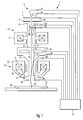
- FIG. 1 is a schematic illustration of an embodiment of a particle beam system.
- the particle beam system 1 comprises a particle beam source 3 including a cathode 5, a suppressor electrode 7 and an extractor electrode 9 for generating an electron beam 11.
- the electron beam 11 emerging from an opening in the extractor electrode 9 is accelerated by an anode 13 to a predetermined kinetic energy and enters a beam tube 15 via an opening in the anode 13.
- the electron beam may traverse a condenser lens 17, an aperture 19 provided in an electron detector 21.
- the electron beam further traverses an objective lens 23 for focusing the electron beam 11 at a location 25 in an object plane 27 of the objective lens 23.
- a surface of an object 29 which is to be inspected or manipulated with the particle beam system 1 can be arranged in the object plane 27.
- the objective lens 23 comprises an annular coil 31, which is arranged in an annular pole piece 33, which comprises an annular upper pole piece 35 and an annular lower pole piece 37 such that a magnetic field focusing the electron beam 11 is generated in an annular gap between the two pole pieces 35 and 37.
- the objective lens further comprises a terminal electrode 39 which is arranged spaced apart from a lower end 41 of the beam tube 15 and has an opening traversed by the electron beam 11.
- a terminal electrode 39 which is arranged spaced apart from a lower end 41 of the beam tube 15 and has an opening traversed by the electron beam 11.
- An electric field generated between the lower end of the beam tube 41 and the terminal electrode 39 decelerates the electrons, propagating inside the beam tube 15 at a high kinetic energy, to a desired lower kinetic energy at which they are incident on the object 29.
- This electric field may provide an additional focusing effect together with the magnetic field.
- the individual components of the particle beam system 1 are controlled by a controller 41.
- the controller is shown in Figure 1 as a functional block and comprises plural control components which can be spatially separated from each other or arranged together in, for example, a housing.
- One component of the controller 41 controls the beam source via connectors 43 for supplying a heating current to the cathode 5 and defining a potential of the cathode. Potentials of the suppressor electrode 7 and the extractor electrode 9 are controlled via connectors 44. An electric potential of the beam tube 15 and the anode 13 is defined by the controller via a connector 45.
- the controller 41 comprises a stabilized high voltage source, which supplies a voltage of, for example, 8 kV with respect to ground to the connector 45.
- a potential of the cathode 5 can be set between, for example, 0 and -10 kV.
- the controller 41 may furthermore apply a fixed or adjustable potential of, for example, 0 to 5 kV via a connector 46 to the terminal electrode 39, and the object 29 can be at ground potential or at a potential different from ground potential.
- Beam deflectors 47 which are controlled by the controller 41 via connectors 48 can be arranged in the objective lens 23.
- the beam deflectors can be magnetic beam deflectors which may provide adjustable deflecting magnetic fields within the beam tube 15 in order to vary the location 25 at which the electron beam 11 is incident on the object 29, and to scan the particle beam 11 across a portion of the surface 27 of the object 29.
- the particle beam 11 incident on the object 29 causes secondary electrons or backscattered electrons to emanate from the object 29. A portion of these electrons may enter the beam tube 15 and can be detected by the electron detector 21.
- An exemplary trajectory of a secondary electron incident on the electron detector 21 is labeled with reference numeral 51 in Figure 1 .
- Detection signals triggered by incident electrons are output by the electron detector 21 at a connector 53 and read in by the controller 41.
- the particle beam source 3 is preferably operated in a stationary mode, i.e. once it is put into operation, the particle beam source 3 is operated for several hours or even days under constant conditions such that the electron beam 11 is continuously generated. However, it is desirable to not allow the electron beam 11 to be constantly incident on the object 29 and to be able to switch the beam on off as required.
- the particle beam system 1 comprises a beam blanker system 55 which comprises a pair of deflector electrodes 56, 57 which can be arranged inside the beam tube 15 such that the electron beam 11 traverses a gap formed between the deflector electrodes 56, 57.
- the controller 41 comprises a component including a control circuit described in detail below, which supplies electric potentials to the deflector electrodes 56, 57 via connectors 58 and 59.
- both deflector electrodes 56, 57 are at the same electric potential, the beam 11 traverses the gap between the deflector electrodes along a straight line.
- the deflector electrodes are at a same electric potential as the beam tube 15.
- the deflector electrodes 56, 57 are at different electric potentials, an electrostatic field is produced between the two deflector electrodes. This electric field deflects the electron beam 11 away from its original trajectory.
- the deflected electron beam is shown in Figure 1 as a broken line 11' and is incident on a plate 61 arranged in the beam tube 15.
- the plate 61 has an aperture which is traversed by the non-deflected beam 11 to be incident on the surface 27 of the object 29.
- the electron beam 11' incident on the plate 61 is absorbed and cannot reach the surface 27 of the object 29.
- controller 41 providing a control circuit 63, which is part of the beam blanker system 55, will be illustrated below with the reference to Figure 2 .
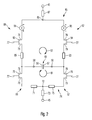
- the two deflection plates 56, 57 form, from an electric point of view, a capacitor 65, which is shown as such in the circuit diagram of Figure 2 .
- the capacitor 65 is connected via the connectors 58 and 59 to the controller 41 which provides two current paths in which the capacitor 65 is arranged.
- a first current path 67 is used for discharging the capacitor 65.
- the following elements are connected in series between the connectors 58 and 59, and the deflection plates 56 and 57, respectively: a first series connection 69 of a switch 70 and a resistor 71, a node 72 connected via a resistor 73 to the terminal 45 connected to the beam tube 15, and a second series connection 74 of a resistor 75 and a switch 76.
- the individual elements of the series connections 69 and 74 can be arranged in any desired order. It is preferable, however, to choose the arrangement order of the individual elements in the respective series connections such that both of the series connections are symmetrically arranged.
- the switches 70 and 76 are in the embodied as MOSFETs and have a function of allowing or blocking a current flow between terminals 78 and 79 of the switch based on a voltage that is applied to a control terminal 77 of the switch 70, 76.
- the switches 70 and 76 can also be realized by other electric switching elements which are capable of allowing and blocking a current flow between two terminals 78 and 79, based on a signal, such as a voltage signal, applied to a control terminal 77.
- the current path 67 is symmetrically arranged with respect to the node 72 connected to the beam tube 15 and to the capacitor 65, in that the series connections 69 and 74 are arranged on both sides of both the node 72 and the capacitor 65. Due to this symmetric arrangement, closure of the switches 70 and 76 when the capacitor 65 is charged does not induce any current to flow from the node 72 via to the connector 45 the resistor 73, which current could affect a potential provided by the high voltage source at the connector 45.
- the high voltage potential supplied to the beam tube 15 remains substantially unchanged when the electron beam 11 is switched on. After the electron beam 11 has been switched on, it is available immediately available and stable as required, such that it can be used for its intended purposes, such as, for example, the inspection or modification of the object 29.
- the control circuit provides a second current path 85 for charging of the capacitor 65.
- the second current path 85 is also symmetrically arranged with respect to the capacitor 65 and a node 86 connected to the connector 45 via a resistor 87, wherein connector 45 is connected to the beam tube 15.
- a series connection 88 is arranged between the connector 58 of the deflection plate 56 and the node 86, wherein the series connection 88 comprises a resistor 89, a switch 90 and a voltage source 91.
- a series connection 92 is arranged between the connector 59 of the deflection plate 57 and the node 86, wherein the series connection 92 comprises a resistor 93, a switch 94 and a voltage source 95.
- the arrangement order of the individual elements 89, 90 and 91, or 93, 94 and 95 in the series connections 88 and 92 is again arbitrary, wherein it can be advantageous to select the arrangement order such that the series connections 88 and 92 have both a symmetric arrangement with respect to one another.
- the switches 90 and 94 are embodied as MOSFETs, but they can also be realized by other electric components which can allow or block a current flow between terminals 78 and 79 depending on a control signal applied to a control terminal 77.
- the two series connections 88 and 92 each form a switchable voltage source which is switched on when the respective switch is closed and which is switched off when the respective switch is opened.
- the voltage sources 91 and 95 supply their output voltages continuously, wherein a magnitude of the output voltages can be adjustable.
- the two voltage sources 91 and 95 each supply a voltage of, for example, 100 V and are oriented such that, when the switches 90 and 94 are closed (and switches 70 and 76 opened) a voltage corresponding to 200 V is applied between the deflection plates 56 and 57 in order to deflect the electron beam 11 and to direct it away from the object 29.
- a current flow in the second current path 85 for charging the capacitor 65 is indicated in Figure 2 by an arrow 81. Due to the symmetric arrangement of the series connections 88 and 92, this current flow does not result in a current flowing to or from the second current path 85 from or to the high voltage source via the node 86, so that the high voltage applied to the beam tube 15 is not affected by switching off the electron beam.
- the electron beam 11 can be switched on and off rapidly without affecting the high voltage applied to the beam tube 15 and without affecting the electro-optical properties of the particle beam system 1, accordingly.
- FIG 3 shows an exemplary embodiment of the voltage sources 91, 95 shown in Figure 2 .
- the voltage source 91, 95 comprises an AC voltage source 101 which is connected to an input winding 103 of a transformer 105 provided for potential separation.
- An output winding 107 of the transformer 105 is connected to a rectifier bridge circuit 109, which provides a DC voltage at outputs 111, 112 of voltage source 91, 95.
- the output voltage is smoothed by a capacitor 113. Due to the use of the transformer 105 it is possible for the AC voltage source 101 to be operated at a lower electric potential, while the rectifier bridge circuit 109 is operated at a high electric potential relative to a ground 117 provided by a high voltage source 115.
- the high voltage source 115 is connected to the node 86 which is connected to an output 112 of the voltage source 91, 95.
- the beam tube 15 is also connected to the node 86 in an electrically conducting manner.
- the circuit shown in Figure 3 continuously provides the voltage at its terminals 111, 112. Together with the switches, which are each connected to the voltage sources in series, two switchable voltage sources are formed. This is similarly possible, however, if a switch is inserted, for example, in the conductor between the AC voltage source 101 and the input winding 103.
- the circuit itself then already forms a switchable voltage source, which provides a switchable voltage at the terminals 111 and 112.
- the series circuits 88 and 92 need not necessarily contain a switch (90 or 94 in Figure 2 ) in order to provide a switchable voltage source.
- Figure 4 illustrates a variation of an embodiment of a deflection system which according to the previous embodiments, comprises a pair of deflection plates.
- a deflection system comprises two pairs of deflection plates, wherein one pair of deflection plates 56, 57 is oriented parallel to each other, wherein the other pair of deflection plates 56', 57' is also oriented parallel to each other, wherein the deflection plates 56 and 56' are oriented orthogonally to each other and wherein the deflection plates 57 and 57' are also oriented orthogonally to each other.
- the particle beam 11 traverses through a center of the deflection plates, wherein an electric potential is applied ton each deflection plate via terminals 58, 58', 59 and 59'.
- terminals 58 and 58' are both connected to the control circuit and the terminals 59 and 59' are likewise both connected to the control circuit, it is possible to deflect the beam 11 at an angle downwards to the right as is indicated by an arrow 121 in Figure 4 .
- the terminals 58, 59 and the terminals 58', 59' can each be connected to different control circuits which provide individually adjustable control voltages, such that the direction 121 into which the beam 11 is deflected can then be adjusted by adjusting the individual voltages of the control circuits.
- the particle beam is an electron beam.
- the particle beam is an electron beam which is provided for modifying samples, by, for example, causing a removal of material from the sample or a deposition of material on the sample.
- the particle beam is an ion beam, which is provided in an ion beam system for inspection or modification of samples.
Landscapes
- Chemical & Material Sciences (AREA)
- Analytical Chemistry (AREA)
- Electron Beam Exposure (AREA)
- Electron Sources, Ion Sources (AREA)
Abstract
Description
- The present application claims priority of Patent Application No.
10 2010 007 777.1, filed February 12, 2010 in Germany, entitled "Particle Beam System", the content of which is hereby incorporated by reference in its entirety. - The invention relates to a particle beam system including an electrostatic beam blanker system.
- A conventional particle beam system includes a particle beam source for generating a particle beam, and a high voltage source for providing an acceleration voltage, in order to accelerate the charged particles of the particle beam that are generated by the particle beam source to a desired kinetic energy. The conventional system further comprises a pair of deflection plates, between which a beam path of the particle beam extends. The first deflection plate of the pair can be connected to a high voltage source, and the second deflection plate of the pair can be selectively connected, via a switch, to this high voltage source or to another voltage source providing an electric potential different from that of the high voltage source. If this second deflection plate is connected to the high voltage source, the particle beam is substantially not affected when traversing the pair of deflection plates and propagates essentially along a straight line. If the second deflection plate is connected to the other voltage source however, an electric field is produced between the two deflection plates. Such electric field deflects the particle beam, so that it is, for example, incident on a plate downstream of the deflection plates and is absorbed by such plate. Depending on a switching state of the switch, the particle beam is selectively available downstream of the plate and can therefore be switched on and off by operating the switch.
- It has been found that immediately after the beam has been switched on, the conventional particle beam system does not provide desired operating characteristics and that the desired operating characteristics are achieved only after a fairly long period of time.
- The present invention has been accomplished taking the above problems into consideration.
- It is an object of the present invention is to provide a particle beam system which provides desired operating characteristics more quickly after changing a state of a beam blanker.
- According to embodiments, a particle beam system comprises a particle beam source for generating a particle beam; a high voltage source; a beam blanker system with at least one pair of deflection plates, between which a beam path of the particle beam extends, and a control circuit, wherein the control circuit provides a first current path between a first deflection plate of the pair and a second deflection plate of the pair, wherein a first node connected to the high voltage source and a second switch are arranged in this order in the first current path starting from the first deflection plate.
- The particle beam can be a beam of positively charged particles, such as, for example, ions, or negatively charged particles, such as, for example, ions or electrons. The high voltage source which supplies a voltage of more than 5 kV, for example. The switches are each configured to selectively allow or interrupt a flow of current between two terminals. The switches may comprise semiconductor switching elements, such as, for example, transistors and MOSFETs. The current paths are provided by electric conductors and electric components, such as resistors and switches which allow a current flow across the path in their closed state and which prevent the current flow across the path in their open state.
- The pair of deflection plates form a capacitor, which is inserted into the first current path. When different voltages are applied to the two deflection plates, in order to deflect the particle beam passing between the two deflection plates, or to switch the beam off in a beam path downstream of the beam blanker system, the capacitor is charged up. In order to switch on the beam, the capacitor must be discharged, so that the two deflection plates are at the same electric potential.
- The control circuit is configured to be symmetric in the sense that in order to discharge the capacitor two switches are closed, one of which is arranged in the discharge current path between the one deflection plate and the node connected to the high voltage source and the other is arranged between the other deflection plate and the node connected to the high voltage source. When switching the two switches from their open states with the capacitor charged to their closed state to discharge the capacitor, a potential of the node connected to the high voltage source is therefore not changed and the capacitor can discharge by a current flow within the first current path, without substantially varying the potential of the node connected to the first voltage source. The discharging of the capacitor has no substantial effect on the high voltage source, which may then provide a predetermined voltage at a constant value. Specifically, the predetermined voltage is then available immediately after discharging of the capacitor and consequently immediately after switching on the particle beam using the beam blanker system, so that the particle beam system also shows its desired properties immediately after the beam is switched on.
- The inventors have recognized that in the conventional particle beam system the activation of the switch and the subsequent discharging of the capacitor formed by the deflection plates of the beam blanker system results in a change in the voltage provided by the high voltage source, such that the provided high is not sufficiently stable. Due to a voltage control of the high voltage source this change can only be compensated for only after some time period. During this time period, the particle beam system does not provide its desired properties.
- Due to the symmetrical configuration of the first current path for discharging the capacitor formed by the two deflection plates, any effect on the high voltage source by the discharge process can be avoided.
- According to embodiments of the particle beam system, a second current path for charging the capacitor formed by the two deflection plates is configured to be symmetric. For this purpose, the control circuit comprises a second current path between the first deflection plate and the second deflection plate, wherein a first series connection of a first voltage source and a third switch, a second node connected to the high voltage source, and a second series connection of a second voltage source and a fourth switch are arranged in the second current path in this order, starting from the first deflection plate.
- The first and second voltage sources can each be provided by, for example, a battery or another voltage source circuit.
- According to embodiments of the invention, resistors are arranged in the first current path symmetrically with respect to the pair of deflection plates and to the node connected to the high voltage source and in series with the first or second switch, respectively. These resistors have a function of dissipating the electric energy stored in the capacitor when it is charged. Resistances of these resistors can be dimensioned to allow the fastest possible discharging of the capacitor. For this purpose, the resistances should not be too small, since an oscillating current flow might then arise between the two deflection plates, and they should not be chosen to be too large, as the discharging of the capacitor might then take too long. Ideally, the resistances are dimensioned such that an oscillating circuit formed by the capacitance of the capacitor, an internal resistances of the first and the second switches in their closed states and an inductance of the conductors used to implement the first current path is critically damped in order to allow a fastest possible discharging of the capacitor. This results in the particle beam can being switched on very rapidly.
- Similarly, the second current path may comprise a pair of resistors, in order to allow rapid charging of the capacitor to switch off the beam. Resistances of the third and fourth resistors in this arrangement may again be dimensioned such that a corresponding oscillating circuit formed by the capacitance of capacitor, internal resistances of the third and the fourth switches in their closed states, internal resistances of the first and second current sources and inductances of the conductors used to implement the second current path is critically damped.
- According to embodiments of the particle beam system, the high voltage source supplies potentials of more than 5 kV, in particular more than 7 kV and further, more than 10 kV. These potentials can be measured for example with respect to a ground potential of the particle beam system, or to a cathode of the particle beam source.
- According to embodiments of the particle beam system, voltages that are provided by the second and/or the third voltage sources have values of more than 10 V, more than 50 V or more than 150 V.
- The forgoing as well as other advantageous features of the invention will be more apparent from the following detailed description of exemplary embodiments of the invention with reference to the accompanying drawings. It is noted that not all possible embodiments of the present invention necessarily exhibit each and every, or any, of the advantages identified herein.
- Figure 1
- is a schematic illustration of a particle beam system according to an embodiment;
- Figure 2
- is a schematic illustration of a detail of a control circuit of a beam blanker system of the particle beam system shown in
Figure 1 ; - Figure 3
- is a schematic illustration of an embodiment of a voltage source; and
- Figure 4
- is a schematic illustration of an embodiment of a beam deflector.
- In the exemplary embodiments described below, components that are alike in function and structure are designated as far as possible by alike reference numerals. Therefore, to understand the features of the individual components of a specific embodiment, the descriptions of other embodiments and of the summary of the invention should be referred to.
-
Figure 1 is a schematic illustration of an embodiment of a particle beam system. Theparticle beam system 1 comprises a particle beam source 3 including acathode 5, asuppressor electrode 7 and anextractor electrode 9 for generating anelectron beam 11. Theelectron beam 11 emerging from an opening in theextractor electrode 9 is accelerated by ananode 13 to a predetermined kinetic energy and enters abeam tube 15 via an opening in theanode 13. - The electron beam may traverse a
condenser lens 17, anaperture 19 provided in anelectron detector 21. The electron beam further traverses anobjective lens 23 for focusing theelectron beam 11 at alocation 25 in anobject plane 27 of theobjective lens 23. A surface of anobject 29 which is to be inspected or manipulated with theparticle beam system 1 can be arranged in theobject plane 27. Theobjective lens 23 comprises anannular coil 31, which is arranged in anannular pole piece 33, which comprises an annularupper pole piece 35 and an annularlower pole piece 37 such that a magnetic field focusing theelectron beam 11 is generated in an annular gap between the twopole pieces terminal electrode 39 which is arranged spaced apart from alower end 41 of thebeam tube 15 and has an opening traversed by theelectron beam 11. An electric field generated between the lower end of thebeam tube 41 and theterminal electrode 39 decelerates the electrons, propagating inside thebeam tube 15 at a high kinetic energy, to a desired lower kinetic energy at which they are incident on theobject 29. This electric field may provide an additional focusing effect together with the magnetic field. - The individual components of the
particle beam system 1 are controlled by acontroller 41. The controller is shown inFigure 1 as a functional block and comprises plural control components which can be spatially separated from each other or arranged together in, for example, a housing. - One component of the
controller 41 controls the beam source viaconnectors 43 for supplying a heating current to thecathode 5 and defining a potential of the cathode. Potentials of thesuppressor electrode 7 and theextractor electrode 9 are controlled viaconnectors 44. An electric potential of thebeam tube 15 and theanode 13 is defined by the controller via aconnector 45. For this purpose, thecontroller 41 comprises a stabilized high voltage source, which supplies a voltage of, for example, 8 kV with respect to ground to theconnector 45. A potential of thecathode 5 can be set between, for example, 0 and -10 kV. Thecontroller 41 may furthermore apply a fixed or adjustable potential of, for example, 0 to 5 kV via aconnector 46 to theterminal electrode 39, and theobject 29 can be at ground potential or at a potential different from ground potential. - Beam deflectors 47 which are controlled by the
controller 41 viaconnectors 48 can be arranged in theobjective lens 23. The beam deflectors can be magnetic beam deflectors which may provide adjustable deflecting magnetic fields within thebeam tube 15 in order to vary thelocation 25 at which theelectron beam 11 is incident on theobject 29, and to scan theparticle beam 11 across a portion of thesurface 27 of theobject 29. - The
particle beam 11 incident on theobject 29 causes secondary electrons or backscattered electrons to emanate from theobject 29. A portion of these electrons may enter thebeam tube 15 and can be detected by theelectron detector 21. - An exemplary trajectory of a secondary electron incident on the
electron detector 21 is labeled withreference numeral 51 inFigure 1 . Detection signals triggered by incident electrons are output by theelectron detector 21 at aconnector 53 and read in by thecontroller 41. - The particle beam source 3 is preferably operated in a stationary mode, i.e. once it is put into operation, the particle beam source 3 is operated for several hours or even days under constant conditions such that the
electron beam 11 is continuously generated. However, it is desirable to not allow theelectron beam 11 to be constantly incident on theobject 29 and to be able to switch the beam on off as required. For this purpose theparticle beam system 1 comprises abeam blanker system 55 which comprises a pair ofdeflector electrodes beam tube 15 such that theelectron beam 11 traverses a gap formed between thedeflector electrodes controller 41 comprises a component including a control circuit described in detail below, which supplies electric potentials to thedeflector electrodes connectors - If both
deflector electrodes beam 11 traverses the gap between the deflector electrodes along a straight line. Preferably, the deflector electrodes are at a same electric potential as thebeam tube 15. - If the
deflector electrodes electron beam 11 away from its original trajectory. The deflected electron beam is shown inFigure 1 as a broken line 11' and is incident on aplate 61 arranged in thebeam tube 15. Theplate 61 has an aperture which is traversed by thenon-deflected beam 11 to be incident on thesurface 27 of theobject 29. The electron beam 11' incident on theplate 61 is absorbed and cannot reach thesurface 27 of theobject 29. - It is therefore possible during the continuous operation of the particle beam source 3 to operate the
particle beam system 1 in a first operating mode in which a same potential is applied by thecontroller 41 to theconnectors object 29, and to operate theparticle beam system 1 in a second operating mode in which different electric potentials are applied by thecontroller 41 to theterminals object 29. - The component of the
controller 41 providing a control circuit 63, which is part of thebeam blanker system 55, will be illustrated below with the reference toFigure 2 . - The two
deflection plates capacitor 65, which is shown as such in the circuit diagram ofFigure 2 . Thecapacitor 65 is connected via theconnectors controller 41 which provides two current paths in which thecapacitor 65 is arranged. A firstcurrent path 67 is used for discharging thecapacitor 65. For this purpose, the following elements are connected in series between theconnectors deflection plates switch 70 and aresistor 71, anode 72 connected via aresistor 73 to the terminal 45 connected to thebeam tube 15, and asecond series connection 74 of aresistor 75 and aswitch 76. The individual elements of theseries connections 69 and 74 can be arranged in any desired order. It is preferable, however, to choose the arrangement order of the individual elements in the respective series connections such that both of the series connections are symmetrically arranged. - In the illustrated embodiment, the
switches terminals control terminal 77 of theswitch switches terminals control terminal 77. - By controlling the two
switches terminals 77 it is possible to set the switches to their closed state, such that the chargedcapacitor 65 can discharge. A corresponding current flow is shown inFigure 2 by anarrow 81. - The
current path 67 is symmetrically arranged with respect to thenode 72 connected to thebeam tube 15 and to thecapacitor 65, in that theseries connections 69 and 74 are arranged on both sides of both thenode 72 and thecapacitor 65. Due to this symmetric arrangement, closure of theswitches capacitor 65 is charged does not induce any current to flow from thenode 72 via to theconnector 45 theresistor 73, which current could affect a potential provided by the high voltage source at theconnector 45. The high voltage potential supplied to thebeam tube 15 remains substantially unchanged when theelectron beam 11 is switched on. After theelectron beam 11 has been switched on, it is available immediately available and stable as required, such that it can be used for its intended purposes, such as, for example, the inspection or modification of theobject 29. - The control circuit provides a second
current path 85 for charging of thecapacitor 65. The secondcurrent path 85 is also symmetrically arranged with respect to thecapacitor 65 and anode 86 connected to theconnector 45 via aresistor 87, whereinconnector 45 is connected to thebeam tube 15. On the left-hand side inFigure 2 , a series connection 88 is arranged between theconnector 58 of thedeflection plate 56 and thenode 86, wherein the series connection 88 comprises aresistor 89, aswitch 90 and avoltage source 91. On the right-hand side inFigure 2 , aseries connection 92 is arranged between theconnector 59 of thedeflection plate 57 and thenode 86, wherein theseries connection 92 comprises aresistor 93, aswitch 94 and avoltage source 95. The arrangement order of theindividual elements series connections 88 and 92 is again arbitrary, wherein it can be advantageous to select the arrangement order such that theseries connections 88 and 92 have both a symmetric arrangement with respect to one another. - In the illustrated embodiment, the
switches terminals control terminal 77. - The two
series connections 88 and 92 each form a switchable voltage source which is switched on when the respective switch is closed and which is switched off when the respective switch is opened. Thevoltage sources - The two
voltage sources switches deflection plates electron beam 11 and to direct it away from theobject 29. A current flow in the secondcurrent path 85 for charging thecapacitor 65 is indicated inFigure 2 by anarrow 81. Due to the symmetric arrangement of theseries connections 88 and 92, this current flow does not result in a current flowing to or from the secondcurrent path 85 from or to the high voltage source via thenode 86, so that the high voltage applied to thebeam tube 15 is not affected by switching off the electron beam. Using the illustrated control circuit, theelectron beam 11 can be switched on and off rapidly without affecting the high voltage applied to thebeam tube 15 and without affecting the electro-optical properties of theparticle beam system 1, accordingly. -
Figure 3 shows an exemplary embodiment of thevoltage sources Figure 2 . According to this embodiment, thevoltage source AC voltage source 101 which is connected to an input winding 103 of atransformer 105 provided for potential separation. An output winding 107 of thetransformer 105 is connected to arectifier bridge circuit 109, which provides a DC voltage atoutputs voltage source capacitor 113. Due to the use of thetransformer 105 it is possible for theAC voltage source 101 to be operated at a lower electric potential, while therectifier bridge circuit 109 is operated at a high electric potential relative to aground 117 provided by ahigh voltage source 115. Thehigh voltage source 115 is connected to thenode 86 which is connected to anoutput 112 of thevoltage source beam tube 15 is also connected to thenode 86 in an electrically conducting manner. - The circuit shown in
Figure 3 continuously provides the voltage at itsterminals AC voltage source 101 and the input winding 103. The circuit itself then already forms a switchable voltage source, which provides a switchable voltage at theterminals series circuits 88 and 92 need not necessarily contain a switch (90 or 94 inFigure 2 ) in order to provide a switchable voltage source. -
Figure 4 illustrates a variation of an embodiment of a deflection system which according to the previous embodiments, comprises a pair of deflection plates. According to the variation shown inFigure 4 , a deflection system comprises two pairs of deflection plates, wherein one pair ofdeflection plates deflection plates 56 and 56' are oriented orthogonally to each other and wherein thedeflection plates 57 and 57' are also oriented orthogonally to each other. Theparticle beam 11 traverses through a center of the deflection plates, wherein an electric potential is applied ton each deflection plate viaterminals terminals 58 and 58' are both connected to the control circuit and theterminals 59 and 59' are likewise both connected to the control circuit, it is possible to deflect thebeam 11 at an angle downwards to the right as is indicated by anarrow 121 inFigure 4 . Likewise theterminals direction 121 into which thebeam 11 is deflected can then be adjusted by adjusting the individual voltages of the control circuits. - The embodiments described above relate to an electron microscope, in which the particle beam is an electron beam. According to further embodiments, the particle beam is an electron beam which is provided for modifying samples, by, for example, causing a removal of material from the sample or a deposition of material on the sample. According to further embodiments, the particle beam is an ion beam, which is provided in an ion beam system for inspection or modification of samples.
- While the invention has been described with respect to certain exemplary embodiments thereof, it is evident that many alternatives, modifications and variations will be apparent to those skilled in the art. Accordingly, the exemplary embodiments of the invention set forth herein are intended to be illustrative and not limiting in any way. Various changes may be made without departing from the scope of the present invention as defined in the following claims.
Claims (15)
- A particle beam system comprising:a particle beam source (3) configured to generate a particle beam (11);a high voltage source; anda beam blanker system (55) comprising a pair of deflection plates (56, 57) and a control circuit;wherein a beam path of the particle beam (11) extends between a first deflection plate (56) of the pair of deflection plates and a second deflection plate (57) of the pair of deflection plates;wherein the control circuit (63) comprises a first switch (70), a second switch (76) and a first node (72) connected to an output terminal of the high voltage source;wherein the control circuit (63) provides a first current path between the first deflection plate (56) and the second deflection plate (57); andwherein the first deflection plate (56), the first switch (70), the first node (72), the second switch (76) and the second deflection plate (57) are arranged in the first current path (67) in this order.
- The particle beam system according to claim 1, wherein the control circuit further comprises a first switchable voltage source (90, 91), a second switchable voltage source (94, 95) and a second node (86) connected to the output terminal of the high voltage source;
wherein the control circuit further provides a second current path between the first deflection plate (56) and the second deflection plate (57); and
wherein the first deflection plate (56), the first switchable voltage source (90, 91), the second node (86), the second switchable voltage source (94, 95) and the second deflection plate (57) are arranged in the second current path (85) in this order. - The particle beam system according to claim 2, wherein the first switchable voltage source comprises a second voltage source (91) and a third switch (90) connected in series, and wherein the second switchable voltage source comprises a third voltage source (95) and a fourth switch (94) connected in series.
- The particle beam system according to claim 3, wherein the first switchable voltage source further comprises a first resistor (89),
wherein the second voltage source, the third switch and the first resistor (89) are connected in series, wherein the second switchable voltage source further comprises a second resistor (93); and
wherein the third voltage source, the fourth switch and the second resistor (93) are connected in series. - The particle beam system according to claim 4, wherein the first resistor (89) and the second resistor (93) have equal resistances; and/or wherein the switchable first voltage source (90, 91) and the switchable second voltage source (94, 95) each provide equal voltages in their switched on states.
- The particle beam system according to one of claims 1 to 5, wherein the control circuit further comprises a third resistor (71) and a fourth resistor (75), wherein the third resistor (71) is arranged in the first current path between the first deflection plate (56) and the first node (72), and
wherein the fourth resistor (75) is arranged in the first current path between the first node (72) and the second deflection plate (57). - The particle beam system according to claim 6, wherein the third resistor (71) and the fourth resistor (75) have equal resistances.
- The particle beam system according to one of claims 1 to 7, further comprising an aperture plate (61) arranged in the beam path of the particle beam downstream of the pair of deflection plates (56, 57), and
wherein the aperture plate is configured and arranged to allow the particle beam (11) to traverse the aperture plate in a first operating state of the particle beam system and to intercept the particle beam in a second operating state of the particle beam system. - The particle beam system according to one of claims 1 to 8, wherein the control circuit provides a first operating mode in which the first switch (70) and the second switch (76) are each in a state that closes the first current path and in which the third switch (90) and the fourth switch (94) are each in a state that interrupts the second current path; and
wherein the control circuit provides a second operating mode in which the first switch (70) and the second switch (76) are each in a state that interrupts the first current path and in which the third switch (90) and the fourth switch (94) are each in a state that closes the second current path. - The particle beam system according to claim 9, further comprising an aperture plate arranged in the beam path of the particle beam downstream of the pair of deflection plates,
wherein the particle beam system has a first operating state and a second operating state,
wherein the aperture plate is configured and arranged to allow the particle beam to traverse the aperture plate in the first operating state of the particle beam system and to intercept the particle beam in the second operating state of the particle beam system, and
wherein the particle beam system is configured to operate the control circuit in the first operating mode in the first operating state, and operate the control circuit in the second operating mode in the second operating state. - The particle beam system according to one of claims 1 to 10, further comprising an objective lens (23) configured to focus the particle beam in a sample plane (27), wherein the objective lens is arranged in the beam path of the particle beam downstream of the pair of deflection plates.
- The particle beam system according to one of claims 1 to 11, wherein the high voltage source is a high voltage source configured to supply a high voltage of more than 5 kV relative to ground potential.
- The particle beam system according to one of claims 1 to 12, further comprising a beam tube (15) connected to the first voltage source, wherein the beam path of the particle beam traverses the beam tube.
- The particle beam system according to one of claims 1 to 13, wherein the particle beam source (3) comprises a cathode (5) and wherein a voltage difference between the cathode and the output terminal of the first voltage source is greater than 5 kV.
- The particle beam system according to one of claims 1 to 14, wherein the second voltage source (91) and the third voltage source (95) are configured to produce voltages of more than 10 V; and/or wherein the second voltage source and the third voltage source are configured to produce voltages of less than 4 kV.
Applications Claiming Priority (1)
| Application Number | Priority Date | Filing Date | Title |
|---|---|---|---|
| DE102010007777A DE102010007777A1 (en) | 2010-02-12 | 2010-02-12 | particle beam |
Publications (3)
| Publication Number | Publication Date |
|---|---|
| EP2360712A2 true EP2360712A2 (en) | 2011-08-24 |
| EP2360712A3 EP2360712A3 (en) | 2017-01-04 |
| EP2360712B1 EP2360712B1 (en) | 2021-05-26 |
Family
ID=43920654
Family Applications (1)
| Application Number | Title | Priority Date | Filing Date |
|---|---|---|---|
| EP11001143.4A Active EP2360712B1 (en) | 2010-02-12 | 2011-02-11 | Particle beam system |
Country Status (4)
| Country | Link |
|---|---|
| US (1) | US8759796B2 (en) |
| EP (1) | EP2360712B1 (en) |
| JP (1) | JP5898406B2 (en) |
| DE (1) | DE102010007777A1 (en) |
Families Citing this family (3)
| Publication number | Priority date | Publication date | Assignee | Title |
|---|---|---|---|---|
| US9312093B1 (en) | 2014-06-27 | 2016-04-12 | Carl Zeiss Microscopy Gmbh | Particle beam device comprising an electrode unit |
| DE102019008249B3 (en) | 2019-11-27 | 2020-11-19 | Carl Zeiss Multisem Gmbh | Particle beam system with a multi-beam deflection device and a beam catcher, method for operating the particle beam system and the associated computer program product |
| JP7460779B2 (en) * | 2020-08-24 | 2024-04-02 | 株式会社日立ハイテク | Charged Particle Beam Device |
Family Cites Families (18)
| Publication number | Priority date | Publication date | Assignee | Title |
|---|---|---|---|---|
| US3925660A (en) * | 1972-05-08 | 1975-12-09 | Richard D Albert | Selectable wavelength X-ray source, spectrometer and assay method |
| US3983397A (en) * | 1972-05-08 | 1976-09-28 | Albert Richard D | Selectable wavelength X-ray source |
| US4007375A (en) * | 1975-07-14 | 1977-02-08 | Albert Richard D | Multi-target X-ray source |
| US4063091A (en) * | 1976-10-18 | 1977-12-13 | American Optical Corporation | High speed switching circuit |
| JPS608581B2 (en) * | 1980-02-22 | 1985-03-04 | 株式会社日立製作所 | Blanking device in electron optical system |
| JPS5971246A (en) * | 1982-10-18 | 1984-04-21 | Nippon Telegr & Teleph Corp <Ntt> | Electron beam defining device |
| JPS6132422A (en) * | 1984-07-24 | 1986-02-15 | Hitachi Ltd | Electron beam lithography equipment |
| JPS61147524A (en) * | 1984-12-21 | 1986-07-05 | Toshiba Corp | Blanking circuit of electron beam exposure apparatus |
| JP3432091B2 (en) * | 1996-11-05 | 2003-07-28 | 日本電子株式会社 | Scanning electron microscope |
| US6278124B1 (en) * | 1998-03-05 | 2001-08-21 | Dupont Photomasks, Inc | Electron beam blanking method and system for electron beam lithographic processing |
| DE10245052A1 (en) * | 2002-09-26 | 2004-04-08 | Leo Elektronenmikroskopie Gmbh | Electron beam source and electron optical apparatus with one |
| GB2414857B (en) | 2004-06-03 | 2009-02-25 | Nanobeam Ltd | Apparatus for blanking a charged particle beam |
| JP2006196260A (en) * | 2005-01-12 | 2006-07-27 | Jeol Ltd | Charged particle beam deflection mechanism and charged particle beam apparatus |
| US7227155B2 (en) | 2005-09-30 | 2007-06-05 | Applied Materials, Inc. | Electrostatic deflection system with impedance matching for high positioning accuracy |
| TWI323004B (en) * | 2005-12-15 | 2010-04-01 | Nuflare Technology Inc | Charged particle beam writing method and apparatus |
| US20090026912A1 (en) | 2007-07-26 | 2009-01-29 | Kla-Tencor Technologies Corporation | Intensity modulated electron beam and application to electron beam blanker |
| JP2009038706A (en) * | 2007-08-03 | 2009-02-19 | Shindengen Electric Mfg Co Ltd | Blanking circuit |
| DE102009008063A1 (en) * | 2009-02-09 | 2010-08-19 | Carl Zeiss Nts Gmbh | particle beam |
-
2010
- 2010-02-12 DE DE102010007777A patent/DE102010007777A1/en not_active Ceased
-
2011
- 2011-02-11 EP EP11001143.4A patent/EP2360712B1/en active Active
- 2011-02-11 US US13/025,556 patent/US8759796B2/en active Active
- 2011-02-14 JP JP2011028518A patent/JP5898406B2/en active Active
Non-Patent Citations (1)
| Title |
|---|
| None |
Also Published As
| Publication number | Publication date |
|---|---|
| EP2360712B1 (en) | 2021-05-26 |
| JP2011165667A (en) | 2011-08-25 |
| DE102010007777A1 (en) | 2011-08-18 |
| US8759796B2 (en) | 2014-06-24 |
| EP2360712A3 (en) | 2017-01-04 |
| JP5898406B2 (en) | 2016-04-06 |
| US20120025093A1 (en) | 2012-02-02 |
Similar Documents
| Publication | Publication Date | Title |
|---|---|---|
| WO2020082861A1 (en) | Low-energy scanning electron microscope system, scanning electron microscope system, and specimen detection method | |
| US10068758B2 (en) | Ion mass separation using RF extraction | |
| JPWO2014181396A1 (en) | Mass spectrometer | |
| TW201342419A (en) | Apparatus and methods for high-resolution electron beam imaging | |
| TW201503210A (en) | Electron beam wafer inspection system and method for operation thereof | |
| US7135677B2 (en) | Beam guiding arrangement, imaging method, electron microscopy system and electron lithography system | |
| JP4527289B2 (en) | Particle optics including detection of Auger electrons | |
| CN102598195B (en) | Distributed Ion Source Accelerating Column | |
| JPH0286036A (en) | ion micro analyzer | |
| KR102006810B1 (en) | Ion beam irradiation apparatus | |
| US8759796B2 (en) | Particle beam system | |
| US20040188630A1 (en) | Deflection system for a particle beam device | |
| US11177108B2 (en) | Charged particle beam application apparatus | |
| US7164139B1 (en) | Wien filter with reduced chromatic aberration | |
| US9991088B2 (en) | Charged particle beam device and aberration corrector | |
| KR100308720B1 (en) | Color compensation particle beam column | |
| WO2016121226A1 (en) | Charged particle beam device and scanning electron microscope | |
| JP7727848B2 (en) | Method and system for screening ions in a mass spectrometer, high voltage pulse circuit and selection circuit - Patents.com | |
| US2632115A (en) | Focusing device for electron microscopes | |
| US12573581B2 (en) | Electron optical column and method for directing a beam of primary electrons onto a sample | |
| JPS61224254A (en) | Charged particle beam device | |
| CN1084041C (en) | particle optics column | |
| KR20260053382A (en) | Optical devices and charged particle beam systems | |
| JPH10199460A (en) | Focused ion beam equipment | |
| JPH03129656A (en) | Secondary ion mass spectrometer |
Legal Events
| Date | Code | Title | Description |
|---|---|---|---|
| PUAI | Public reference made under article 153(3) epc to a published international application that has entered the european phase |
Free format text: ORIGINAL CODE: 0009012 |
|
| PUAI | Public reference made under article 153(3) epc to a published international application that has entered the european phase |
Free format text: ORIGINAL CODE: 0009012 |
|
| AK | Designated contracting states |
Kind code of ref document: A2 Designated state(s): AL AT BE BG CH CY CZ DE DK EE ES FI FR GB GR HR HU IE IS IT LI LT LU LV MC MK MT NL NO PL PT RO RS SE SI SK SM TR |
|
| AX | Request for extension of the european patent |
Extension state: BA ME |
|
| PUAL | Search report despatched |
Free format text: ORIGINAL CODE: 0009013 |
|
| AK | Designated contracting states |
Kind code of ref document: A3 Designated state(s): AL AT BE BG CH CY CZ DE DK EE ES FI FR GB GR HR HU IE IS IT LI LT LU LV MC MK MT NL NO PL PT RO RS SE SI SK SM TR |
|
| AX | Request for extension of the european patent |
Extension state: BA ME |
|
| RIC1 | Information provided on ipc code assigned before grant |
Ipc: H01J 37/24 20060101ALI20161130BHEP Ipc: H01J 37/317 20060101ALI20161130BHEP Ipc: H01J 37/26 20060101ALI20161130BHEP Ipc: H01J 37/04 20060101AFI20161130BHEP |
|
| STAA | Information on the status of an ep patent application or granted ep patent |
Free format text: STATUS: REQUEST FOR EXAMINATION WAS MADE |
|
| 17P | Request for examination filed |
Effective date: 20170704 |
|
| RBV | Designated contracting states (corrected) |
Designated state(s): AL AT BE BG CH CY CZ DE DK EE ES FI FR GB GR HR HU IE IS IT LI LT LU LV MC MK MT NL NO PL PT RO RS SE SI SK SM TR |
|
| STAA | Information on the status of an ep patent application or granted ep patent |
Free format text: STATUS: EXAMINATION IS IN PROGRESS |
|
| 17Q | First examination report despatched |
Effective date: 20180628 |
|
| GRAP | Despatch of communication of intention to grant a patent |
Free format text: ORIGINAL CODE: EPIDOSNIGR1 |
|
| STAA | Information on the status of an ep patent application or granted ep patent |
Free format text: STATUS: GRANT OF PATENT IS INTENDED |
|
| INTG | Intention to grant announced |
Effective date: 20201211 |
|
| RAP1 | Party data changed (applicant data changed or rights of an application transferred) |
Owner name: CARL ZEISS MICROSCOPY GMBH |
|
| GRAS | Grant fee paid |
Free format text: ORIGINAL CODE: EPIDOSNIGR3 |
|
| GRAA | (expected) grant |
Free format text: ORIGINAL CODE: 0009210 |
|
| STAA | Information on the status of an ep patent application or granted ep patent |
Free format text: STATUS: THE PATENT HAS BEEN GRANTED |
|
| AK | Designated contracting states |
Kind code of ref document: B1 Designated state(s): AL AT BE BG CH CY CZ DE DK EE ES FI FR GB GR HR HU IE IS IT LI LT LU LV MC MK MT NL NO PL PT RO RS SE SI SK SM TR |
|
| REG | Reference to a national code |
Ref country code: GB Ref legal event code: FG4D |
|
| REG | Reference to a national code |
Ref country code: CH Ref legal event code: EP |
|
| REG | Reference to a national code |
Ref country code: DE Ref legal event code: R096 Ref document number: 602011071003 Country of ref document: DE |
|
| REG | Reference to a national code |
Ref country code: IE Ref legal event code: FG4D |
|
| REG | Reference to a national code |
Ref country code: LT Ref legal event code: MG9D |
|
| PG25 | Lapsed in a contracting state [announced via postgrant information from national office to epo] |
Ref country code: FI Free format text: LAPSE BECAUSE OF FAILURE TO SUBMIT A TRANSLATION OF THE DESCRIPTION OR TO PAY THE FEE WITHIN THE PRESCRIBED TIME-LIMIT Effective date: 20210526 Ref country code: LT Free format text: LAPSE BECAUSE OF FAILURE TO SUBMIT A TRANSLATION OF THE DESCRIPTION OR TO PAY THE FEE WITHIN THE PRESCRIBED TIME-LIMIT Effective date: 20210526 Ref country code: HR Free format text: LAPSE BECAUSE OF FAILURE TO SUBMIT A TRANSLATION OF THE DESCRIPTION OR TO PAY THE FEE WITHIN THE PRESCRIBED TIME-LIMIT Effective date: 20210526 Ref country code: BG Free format text: LAPSE BECAUSE OF FAILURE TO SUBMIT A TRANSLATION OF THE DESCRIPTION OR TO PAY THE FEE WITHIN THE PRESCRIBED TIME-LIMIT Effective date: 20210826 |
|
| REG | Reference to a national code |
Ref country code: NL Ref legal event code: MP Effective date: 20210526 |
|
| PG25 | Lapsed in a contracting state [announced via postgrant information from national office to epo] |
Ref country code: NO Free format text: LAPSE BECAUSE OF FAILURE TO SUBMIT A TRANSLATION OF THE DESCRIPTION OR TO PAY THE FEE WITHIN THE PRESCRIBED TIME-LIMIT Effective date: 20210826 Ref country code: PT Free format text: LAPSE BECAUSE OF FAILURE TO SUBMIT A TRANSLATION OF THE DESCRIPTION OR TO PAY THE FEE WITHIN THE PRESCRIBED TIME-LIMIT Effective date: 20210927 Ref country code: PL Free format text: LAPSE BECAUSE OF FAILURE TO SUBMIT A TRANSLATION OF THE DESCRIPTION OR TO PAY THE FEE WITHIN THE PRESCRIBED TIME-LIMIT Effective date: 20210526 Ref country code: IS Free format text: LAPSE BECAUSE OF FAILURE TO SUBMIT A TRANSLATION OF THE DESCRIPTION OR TO PAY THE FEE WITHIN THE PRESCRIBED TIME-LIMIT Effective date: 20210926 Ref country code: GR Free format text: LAPSE BECAUSE OF FAILURE TO SUBMIT A TRANSLATION OF THE DESCRIPTION OR TO PAY THE FEE WITHIN THE PRESCRIBED TIME-LIMIT Effective date: 20210827 Ref country code: LV Free format text: LAPSE BECAUSE OF FAILURE TO SUBMIT A TRANSLATION OF THE DESCRIPTION OR TO PAY THE FEE WITHIN THE PRESCRIBED TIME-LIMIT Effective date: 20210526 Ref country code: SE Free format text: LAPSE BECAUSE OF FAILURE TO SUBMIT A TRANSLATION OF THE DESCRIPTION OR TO PAY THE FEE WITHIN THE PRESCRIBED TIME-LIMIT Effective date: 20210526 Ref country code: RS Free format text: LAPSE BECAUSE OF FAILURE TO SUBMIT A TRANSLATION OF THE DESCRIPTION OR TO PAY THE FEE WITHIN THE PRESCRIBED TIME-LIMIT Effective date: 20210526 |
|
| PG25 | Lapsed in a contracting state [announced via postgrant information from national office to epo] |
Ref country code: NL Free format text: LAPSE BECAUSE OF FAILURE TO SUBMIT A TRANSLATION OF THE DESCRIPTION OR TO PAY THE FEE WITHIN THE PRESCRIBED TIME-LIMIT Effective date: 20210526 |
|
| PG25 | Lapsed in a contracting state [announced via postgrant information from national office to epo] |
Ref country code: RO Free format text: LAPSE BECAUSE OF FAILURE TO SUBMIT A TRANSLATION OF THE DESCRIPTION OR TO PAY THE FEE WITHIN THE PRESCRIBED TIME-LIMIT Effective date: 20210526 Ref country code: ES Free format text: LAPSE BECAUSE OF FAILURE TO SUBMIT A TRANSLATION OF THE DESCRIPTION OR TO PAY THE FEE WITHIN THE PRESCRIBED TIME-LIMIT Effective date: 20210526 Ref country code: DK Free format text: LAPSE BECAUSE OF FAILURE TO SUBMIT A TRANSLATION OF THE DESCRIPTION OR TO PAY THE FEE WITHIN THE PRESCRIBED TIME-LIMIT Effective date: 20210526 Ref country code: EE Free format text: LAPSE BECAUSE OF FAILURE TO SUBMIT A TRANSLATION OF THE DESCRIPTION OR TO PAY THE FEE WITHIN THE PRESCRIBED TIME-LIMIT Effective date: 20210526 Ref country code: CZ Free format text: LAPSE BECAUSE OF FAILURE TO SUBMIT A TRANSLATION OF THE DESCRIPTION OR TO PAY THE FEE WITHIN THE PRESCRIBED TIME-LIMIT Effective date: 20210526 Ref country code: SK Free format text: LAPSE BECAUSE OF FAILURE TO SUBMIT A TRANSLATION OF THE DESCRIPTION OR TO PAY THE FEE WITHIN THE PRESCRIBED TIME-LIMIT Effective date: 20210526 Ref country code: SM Free format text: LAPSE BECAUSE OF FAILURE TO SUBMIT A TRANSLATION OF THE DESCRIPTION OR TO PAY THE FEE WITHIN THE PRESCRIBED TIME-LIMIT Effective date: 20210526 |
|
| REG | Reference to a national code |
Ref country code: DE Ref legal event code: R097 Ref document number: 602011071003 Country of ref document: DE |
|
| PLBE | No opposition filed within time limit |
Free format text: ORIGINAL CODE: 0009261 |
|
| STAA | Information on the status of an ep patent application or granted ep patent |
Free format text: STATUS: NO OPPOSITION FILED WITHIN TIME LIMIT |
|
| 26N | No opposition filed |
Effective date: 20220301 |
|
| PG25 | Lapsed in a contracting state [announced via postgrant information from national office to epo] |
Ref country code: IS Free format text: LAPSE BECAUSE OF FAILURE TO SUBMIT A TRANSLATION OF THE DESCRIPTION OR TO PAY THE FEE WITHIN THE PRESCRIBED TIME-LIMIT Effective date: 20210926 Ref country code: AL Free format text: LAPSE BECAUSE OF FAILURE TO SUBMIT A TRANSLATION OF THE DESCRIPTION OR TO PAY THE FEE WITHIN THE PRESCRIBED TIME-LIMIT Effective date: 20210526 |
|
| PG25 | Lapsed in a contracting state [announced via postgrant information from national office to epo] |
Ref country code: IT Free format text: LAPSE BECAUSE OF FAILURE TO SUBMIT A TRANSLATION OF THE DESCRIPTION OR TO PAY THE FEE WITHIN THE PRESCRIBED TIME-LIMIT Effective date: 20210526 |
|
| PG25 | Lapsed in a contracting state [announced via postgrant information from national office to epo] |
Ref country code: MC Free format text: LAPSE BECAUSE OF FAILURE TO SUBMIT A TRANSLATION OF THE DESCRIPTION OR TO PAY THE FEE WITHIN THE PRESCRIBED TIME-LIMIT Effective date: 20210526 |
|
| REG | Reference to a national code |
Ref country code: CH Ref legal event code: PL |
|
| REG | Reference to a national code |
Ref country code: BE Ref legal event code: MM Effective date: 20220228 |
|
| GBPC | Gb: european patent ceased through non-payment of renewal fee |
Effective date: 20220211 |
|
| PG25 | Lapsed in a contracting state [announced via postgrant information from national office to epo] |
Ref country code: LU Free format text: LAPSE BECAUSE OF NON-PAYMENT OF DUE FEES Effective date: 20220211 |
|
| PG25 | Lapsed in a contracting state [announced via postgrant information from national office to epo] |
Ref country code: FR Free format text: LAPSE BECAUSE OF NON-PAYMENT OF DUE FEES Effective date: 20220228 |
|
| PG25 | Lapsed in a contracting state [announced via postgrant information from national office to epo] |
Ref country code: LI Free format text: LAPSE BECAUSE OF NON-PAYMENT OF DUE FEES Effective date: 20220228 Ref country code: IE Free format text: LAPSE BECAUSE OF NON-PAYMENT OF DUE FEES Effective date: 20220211 Ref country code: GB Free format text: LAPSE BECAUSE OF NON-PAYMENT OF DUE FEES Effective date: 20220211 Ref country code: CH Free format text: LAPSE BECAUSE OF NON-PAYMENT OF DUE FEES Effective date: 20220228 |
|
| PG25 | Lapsed in a contracting state [announced via postgrant information from national office to epo] |
Ref country code: BE Free format text: LAPSE BECAUSE OF NON-PAYMENT OF DUE FEES Effective date: 20220228 |
|
| PG25 | Lapsed in a contracting state [announced via postgrant information from national office to epo] |
Ref country code: HU Free format text: LAPSE BECAUSE OF FAILURE TO SUBMIT A TRANSLATION OF THE DESCRIPTION OR TO PAY THE FEE WITHIN THE PRESCRIBED TIME-LIMIT; INVALID AB INITIO Effective date: 20110211 |
|
| PG25 | Lapsed in a contracting state [announced via postgrant information from national office to epo] |
Ref country code: MK Free format text: LAPSE BECAUSE OF FAILURE TO SUBMIT A TRANSLATION OF THE DESCRIPTION OR TO PAY THE FEE WITHIN THE PRESCRIBED TIME-LIMIT Effective date: 20210526 Ref country code: CY Free format text: LAPSE BECAUSE OF FAILURE TO SUBMIT A TRANSLATION OF THE DESCRIPTION OR TO PAY THE FEE WITHIN THE PRESCRIBED TIME-LIMIT Effective date: 20210526 |
|
| PG25 | Lapsed in a contracting state [announced via postgrant information from national office to epo] |
Ref country code: TR Free format text: LAPSE BECAUSE OF FAILURE TO SUBMIT A TRANSLATION OF THE DESCRIPTION OR TO PAY THE FEE WITHIN THE PRESCRIBED TIME-LIMIT Effective date: 20210526 |
|
| PG25 | Lapsed in a contracting state [announced via postgrant information from national office to epo] |
Ref country code: MT Free format text: LAPSE BECAUSE OF FAILURE TO SUBMIT A TRANSLATION OF THE DESCRIPTION OR TO PAY THE FEE WITHIN THE PRESCRIBED TIME-LIMIT Effective date: 20210526 |
|
| REG | Reference to a national code |
Ref country code: AT Ref legal event code: MK05 Ref document number: 1831757 Country of ref document: AT Kind code of ref document: T Effective date: 20210526 |
|
| PG25 | Lapsed in a contracting state [announced via postgrant information from national office to epo] |
Ref country code: AT Free format text: LAPSE BECAUSE OF FAILURE TO SUBMIT A TRANSLATION OF THE DESCRIPTION OR TO PAY THE FEE WITHIN THE PRESCRIBED TIME-LIMIT Effective date: 20210526 |
|
| PGFP | Annual fee paid to national office [announced via postgrant information from national office to epo] |
Ref country code: DE Payment date: 20260218 Year of fee payment: 16 |