EP2360449A1 - Microelectromechanical gyrospcope with inversion of actuation forces, and method for actuating a microelectromechanical gyroscope - Google Patents
Microelectromechanical gyrospcope with inversion of actuation forces, and method for actuating a microelectromechanical gyroscope Download PDFInfo
- Publication number
- EP2360449A1 EP2360449A1 EP11154752A EP11154752A EP2360449A1 EP 2360449 A1 EP2360449 A1 EP 2360449A1 EP 11154752 A EP11154752 A EP 11154752A EP 11154752 A EP11154752 A EP 11154752A EP 2360449 A1 EP2360449 A1 EP 2360449A1
- Authority
- EP
- European Patent Office
- Prior art keywords
- driving
- mass
- gyroscope
- sensing
- signals
- Prior art date
- Legal status (The legal status is an assumption and is not a legal conclusion. Google has not performed a legal analysis and makes no representation as to the accuracy of the status listed.)
- Granted
Links
Images


Classifications
-
- G—PHYSICS
- G01—MEASURING; TESTING
- G01C—MEASURING DISTANCES, LEVELS OR BEARINGS; SURVEYING; NAVIGATION; GYROSCOPIC INSTRUMENTS; PHOTOGRAMMETRY OR VIDEOGRAMMETRY
- G01C19/00—Gyroscopes; Turn-sensitive devices using vibrating masses; Turn-sensitive devices without moving masses; Measuring angular rate using gyroscopic effects
- G01C19/56—Turn-sensitive devices using vibrating masses, e.g. vibratory angular rate sensors based on Coriolis forces
- G01C19/5719—Turn-sensitive devices using vibrating masses, e.g. vibratory angular rate sensors based on Coriolis forces using planar vibrating masses driven in a translation vibration along an axis
- G01C19/5726—Signal processing
-
- G—PHYSICS
- G01—MEASURING; TESTING
- G01C—MEASURING DISTANCES, LEVELS OR BEARINGS; SURVEYING; NAVIGATION; GYROSCOPIC INSTRUMENTS; PHOTOGRAMMETRY OR VIDEOGRAMMETRY
- G01C19/00—Gyroscopes; Turn-sensitive devices using vibrating masses; Turn-sensitive devices without moving masses; Measuring angular rate using gyroscopic effects
- G01C19/56—Turn-sensitive devices using vibrating masses, e.g. vibratory angular rate sensors based on Coriolis forces
- G01C19/5719—Turn-sensitive devices using vibrating masses, e.g. vibratory angular rate sensors based on Coriolis forces using planar vibrating masses driven in a translation vibration along an axis
- G01C19/5733—Structural details or topology
- G01C19/5755—Structural details or topology the devices having a single sensing mass
- G01C19/5762—Structural details or topology the devices having a single sensing mass the sensing mass being connected to a driving mass, e.g. driving frames
Definitions
- MEMS microelectromechanical systems
- MEMS of this type are usually based upon microelectromechanical structures comprising at least one movable mass connected to a fixed body (stator) by springs and movable with respect to the stator according to pre-determined degrees of freedom.
- the movable mass is moreover coupled to the fixed body via capacitive structures (capacitors).
- Capacitors The movement of the movable mass with respect to the fixed body, for example on account of an external stress, modifies the capacitance of the capacitors; from this it is possible to trace back to the relative displacement of the movable mass with respect to the fixed body and hence to the force applied.
- by supplying appropriate biasing voltages it is possible to apply an electrostatic force to the movable mass to set it in motion.
- the frequency response of inertial MEMS structures is exploited, which is typically of the second-order low-pass type.
- MEMS in particular, all electromechanical oscillators and gyroscopes
- driving devices that have the task of maintaining the movable mass in oscillation.
- a first type of known solution envisages supplying, in open loop, periodic stresses at the resonance frequency of the MEMS structure.
- the solution is simple, but also far from effective, because the resonance frequency is not known with precision on account of the ineliminable dispersions in the processes of micromachining of semiconductors.
- the resonance frequency of each individual device can vary over time, for example, on account of temperature gradients or, more simply, on account of ageing.
- gyroscopes have a complex electromechanical structure, which comprises two masses that are movable with respect to the stator and are coupled to one another so as to present a relative degree of freedom.
- the two movable masses are both capacitively coupled to the stator.
- One of the movable masses is dedicated to driving (driving mass) and is kept in oscillation at the resonance frequency.
- the other movable mass (sensing mass) is driven in the oscillatory motion and, in the case of rotation of the microstructure with respect to a pre-determined axis with an angular velocity, is subject to a Coriolis force proportional to the angular velocity itself.
- the sensing mass operates as an accelerometer that enables sensing of the Coriolis acceleration.
- the patent No. EP 1 624 285 describes a system for controlling the velocity of oscillation of the gyroscope, comprising a differential sense amplifier, a high-pass amplifier, and an actuation and control stage, operating in a continuous-time mode.
- control loop comprises a low-pass filter in order to reduce the offset and the effects of parasitic components and couplings by operating on the overall gain and phase of the feedback loop.
- interferences may arise between first voltages, applied to obtain the electrostatic forces necessary to sustain the oscillation, and second voltages, supplied for reading the position of the driving mass.
- the aim of the present invention is to provide a microelectromechanical gyroscope and a method for actuating a microelectromechanical gyroscope that will make it possible to overcome the limitations described.
- a microelectromechanical gyroscope and a method for actuating a microelectromechanical gyroscope are provided as claimed, respectively, in Claim 1 and Claim 13.
- the microstructure 2 is made of semiconductor material and comprises a fixed structure 6, a driving mass 7, and at least one sensing mass 8.
- a uniaxial gyroscope in which a single sensing mass 8 is present.
- What is described hereinafter applies, however, also to the case of multiaxial gyroscopes, which comprise two or more sensing masses or systems of sensing masses, for detecting rotations according to respective independent axes.
- the driving mass 7 is elastically constrained to the fixed structure 6 so as to be able to oscillate about a rest position according to a translational or rotational degree of freedom.
- the sensing mass 8 is mechanically coupled to the driving mass 7 so as to be drawn in motion according to the degree of freedom of the driving mass 7 itself.
- the sensing mass 8 is elastically constrained to the driving mass 7 so as to oscillate in turn with respect to the driving mass 7 itself, with a respective further degree of freedom.
- the driving mass 7 is linearly movable along a driving axis X, while the sensing mass 8 is movable with respect to the driving mass 7 according to a sensing axis Y perpendicular to the driving axis x.
- the type of movement (translational or rotational) allowed by the degrees of freedom and the arrangement of the driving and sensing axes can vary according to the type of gyroscope.
- the expression “according to an axis” will be indifferently used in relation to movements along an axis or about an axis, i.e., movements allowed to the masses by the respective degrees of freedom that are translational (along an axis) or else rotational (about an axis).
- the expression “according to a degree of freedom” will be indifferently used in relation to translational or rotational movements, as allowed by the degree of freedom itself.
- the driving mass 7 (with the sensing mass 8) is connected to the fixed structure 6 so as to define a resonant mechanical system with a resonance frequency ⁇ R (according to the driving axis X).
- the driving mass 7 ( Figure 2 ) is capacitively coupled to the fixed structure 6 thorugh driving units 10 and feedback-sensing units 12.
- the capacitive coupling is of a differential type.
- the actuation units 10 comprise first and second fixed driving electrodes 10a, 10b, which are anchored to the fixed structure 6 and extend substantially perpendicular to the driving direction X, and movable driving electrodes 10c, which are anchored to the driving mass 7 and are also substantially perpendicular to the driving direction X.
- the movable driving electrodes 10c are comb-fingered and capacitively coupled with respective first fixed driving electrodes 10a and second fixed driving electrodes 10b.
- the first and second fixed driving electrodes 10a, 10b of the actuation units 10 are electrically connected to a first driving terminal 13a and to a second driving terminal 13b, respectively, of the microstructure 2.
- the coupling is of a differential type.
- each actuation unit 10 a movement of the driving mass 7 along the driving axis X determines the increase of capacitance between the movable driving electrode 10c and one of the fixed driving electrodes 10a, 10b.
- the capacitance between the movable driving electrode 10c and the other of the fixed driving electrodes 10a, 10b decreases instead accordingly.
- the structure of the feedback-sensing units 12 is similar to that of the actuation units 10.
- the feedback-sensing units 12 comprise first and second fixed sensing electrodes 12a, 12b, anchored to the fixed structure 6, and movable sensing electrodes 12c, anchored to the driving mass 7 and comb-fingered and capacitively coupled with respective first fixed sensing electrodes 12a and second fixed sensing electrodes 12b.
- the first and second fixed sensing electrodes 12a, 12b of the feedback-sensing units 12 are electrically connected, respectively, to a first feedback-sensing terminal 14a and a second feedback-sensing terminal 14b of the microstructure 2.
- the driving mass 7 is coupled to the driving terminals 13a, 13b through differential driving capacitances C D1 , C D2 and to the sensing terminals 14a, 14b through feedback-sensing differential capacitances C FBS1 , C FBS2 .
- the sensing mass 8 is electrically connected to the driving mass 7, without interposition of insulating structures. Consequently, the sensing mass 8 and the driving mass 7 are at the same potential.
- the sensing mass 8 is moreover capacitively coupled to the fixed structure 6 thorugh signal-sensing units 15 ( Figure 3 ). More precisely, the signal-sensing units 15 comprise third and fourth fixed sensing electrodes 15a, 15b, anchored to the fixed structure 6, and movable sensing electrodes 15c, anchored to the sensing mass 8 and arranged between respective third fixed sensing electrodes 15a and fourth fixed sensing electrodes 15b.
- the capacitive coupling is of a differential type, but is obtained thorugh parallel-plate electrodes, perpendicular to the sensing direction Y.
- the third and fourth fixed sensing electrodes 15a, 15b of the signal-sensing units 15 are electrically connected, respectively, to a first signal-sensing terminal 17a and to a second signal-sensing terminal 17b of the microstructure 2.
- the sensing mass 8 is coupled to the signal-sensing terminals 17a, 17b through signal-sensing differential capacitances C SS1 , C SS2 .
- the driving device 3 is connected to the driving terminals 13a, 13b and to the feedback-sensing terminals 14a, 14b of the microstructure 2 so as to form, with the driving mass 7, an oscillating microelectromechanical loop 18, with control of position of the driving mass 7.
- the driving device 3 comprises a charge amplifier 20, a first phase-shifter module 21, a low-pass filter 22, an actuation stage 23, a controller 24, a comparator 25, and a phase-locked-loop (PLL) circuit 27.
- PLL phase-locked-loop
- an oscillator 28 and a timing generator 30, controlled by the PLL circuit 27, are used for supplying timing signals for the driving device 3, for the read generator 4, and for the read device 5.
- the microelectromechanical loop 18 is of a hybrid type.
- the charge amplifier 20 is, in fact, of the switched-capacitor type and is configured to operate in discrete time, whereas the low-pass filter 22 and the actuation stage 23 operate in continuous time.
- the first phase-shifter module 21 carries out the time-discrete-to-time-continous conversion.
- the discrete-time part of the microelectromechanical loop 18 is cyclically actuated according to the correlated-double-sampling (CDS) technique, which comprises, for each cycle:
- the phase-shifter module 21 and the low-pass filter 22 carry out a conditioning of the feedback voltages V FB1, V FB2 .
- the phase-shifter module 21 is cascaded to the charge amplifier 20 and introduces a phase shift that is as close as possible to 90° and in any case comprised in the interval 90° ⁇ 40°.
- the phase-shifter module 21 comprises a sample-and-hold circuit and is moreover configured so as to carry out a first low-pass filtering.
- Phase-shifted feedback voltages V FB1' , V FB2' supplied by the phase-shifter module 21 are thus delayed and attenuated with respect to the feedback voltages V FB1 , V FB2 .
- the phase-shifted feedback voltages V FB1' , V FB2 ' present basically step-like variations.
- the low-pass filter 22 is arranged downstream of the phase-shifter module 21, is a second-order fully differential filter and supplies filtered feedback voltages V FB1 ", V FB2 " which are continuously variable in time.
- the cut-off frequency of the low-pass filter 22 is selected in such a way that the frequency of oscillation of the microelectromechanical loop 18 (in particular, of the driving mass 7), hereinafter referred to as driving frequency ⁇ D , is included in the passband and in such a way that the phase of the useful signal indicating the position x of the driving mass 7 is not substantially altered.
- the passband of the low-pass filter 22 is such that the undesirable signal components, linked to sampling by discrete-time reading, are attenuated by at least 30 dB.
- both the phase-shifter module 21 and the low-pass filter 22 are based upon amplifiers provided with auto-zero function.
- the actuation stage 23 is of a continuous-time fully differential type and has a variable gain.
- the actuation stage 23 is cascaded to the low-pass filter 22 and has outputs connected to the driving terminals 13a, 13b of the microstructure 2 for supplying driving voltages V D1 , V D2 such as to sustain the oscillation of the microelectromechanical loop 18 at the driving frequency ⁇ D , which is close to the mechanical resonance frequency ⁇ R of the microstructure 2.
- the gain G of the actuation stage 23 is determined by the controller 24 through a control signal V c correlated to the filtered feedback voltages V FB1 " , V FB2 " supplied by the low-pass filter 22.
- the actuation stage 23 is configured to invert the sign of the differential a.c. components of the driving voltages V D1 , V D2 in each CDS cycle during the sensing step.
- the comparator 25 has inputs connected to the inputs of the actuation stage 23, which define control nodes 25a, and receives the difference voltage ⁇ V between the filtered feedback voltages V FB1 ", V FB2 " at output from the low-pass filter 22.
- the comparator 25 switches at each zero crossing of the difference voltage ⁇ V, thus operating as frequency-detector device.
- the comparator 25 is connected to a single control node and switches at each zero crossing of one between the filtered feedback voltages V FB1 ", V FB2 " (the zero crossings of the filtered feedback voltages V FB1 ", V FB2 " and of the difference voltage ⁇ V coincide).
- the output of the comparator 25, which supplies a native clock signal CK N is connected to an input of the PLL circuit 27 so as to enable phase locking with the microelectromechanical loop 18.
- the native clock signal CK N is, however, phase-shifted with respect to the driving mass, on account of the presence of the charge amplifier 20, of the first phase-shifter module 21, and of the low-pass filter 22.
- the quadrature clock signal CK 90 has the same frequency and is phase-shifted by 90° with respect to the native clock signal CK N and is used for timing the controller 24. In practice, the quadrature clock signal CK 90 switches at the maxima and at the minima of the filtered feedback voltages V FB1 ", V FB2 " at output from the low-pass filter 22.
- the controller 24 is thus properly timed so as to detect the peak values of the difference voltage ⁇ V between the filtered feedback voltages V FB1 ", V FB2 ".
- the oscillator 28 provides the timing generator 30 with an auxiliary clock signal CK AUX having a calibrated frequency, close to the master frequency ⁇ M .
- the timing generator 30 receives the master clock signal CK M and the auxiliary clock signal CK AUX and uses them for generating the timing signals necessary for the discrete-time components and, more in general, for proper operation of the gyroscope 1.
- the auxiliary clock signal is used when the PLL circuit 27 is not synchronized with the oscillations of the microelectromechanical loop 18 and thus the master clock signal CK M is not available, as, for example, during steps of start-up or reset following upon impact.
- the master clock signal CK M is used when the oscillations of the microelectromechanical loop 18 are stabilized at the driving frequency ⁇ D .
- the timing generator 30 supplies a first timing signal ⁇ 1 , a second timing signal ⁇ 2 , a third timing signal ⁇ 3 , and a fourth timing signal ⁇ 4 , which, in steady-state conditions, have a frequency equal to an integer multiple of the frequency of the native clock signal CK N (for example, 40 ⁇ D ).
- the first, second and third timing signals ⁇ 1 , ⁇ 2 , ⁇ 3 define the reset step, the offset-sampling step, and the sensing step for actuation in accordance with the CDS technique.
- the third timing signal ⁇ 3 is used also to drive the read generator 4 so as to privide the driving mass 7 and the sensing mass 8 with a square-wave read signal V R of a duration equal to the duration of the sensing step.
- the read signal V R is a voltage that varies between 0 V and 2V CM , where V CM is a common-mode voltage for the components of the microelectromechanical loop 18.
- the fourth timing signal ⁇ 4 drives the inversion of sign of the differential components of the driving voltages V D1 , V D2 .
- the temporal correlation between the read signal V R and the timing signals ⁇ 1 , ⁇ 2 , ⁇ 3 , ⁇ 4 is illustrated in Figure 4 and is defined to implement sensing and control cycles according to the CDS technique.
- the first and second timing signals ⁇ 1 , ⁇ 2 are high in a first fraction (t 0 -t 1 ) of each cycle (approximately one fifth of the period, reset step), whilst the third timing signal ⁇ 3 and the fourth timing signal ⁇ 4 are low.
- the fourth timing signal ⁇ 4 switches slightly in advance.
- the fourth timing signal ⁇ 4 has a second edge (in this case the trailing edge) in advance with respect to the third timing signal ⁇ 3 .
- this solution has the purpose of compensating spurious charge injections due to the switching of the driving voltages V D1 , V D2 and to the presence of parasitic capacitive couplings between the driving terminals 13a, 13b and the signal-sensing terminals 17a, 17b.
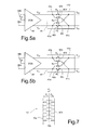
- FIGS 5a, 5b illustrate in greater detail the actuation stage 23, which comprises a fully differential variable-gain amplifier (VGA) 40 and a switching module 41.
- VGA variable-gain amplifier
- the variable-gain amplifier 40 has signal inputs 40a, 40b, connected to the low-pass filter 22 for receiving the filtered feedback voltages V FB1 ", V FB2 ", and a gain-control input 40c, connected to the controller 24 for receiving the control signal V c .
- the outputs of the variable-gain amplifier 40 supply amplified voltages V A1 , V A2 , the difference of which is proportional, according to the gain determined by the control signal V c , to the difference between the filtered feedback voltages V FB1 ", V FB2 ".
- the amplified voltages V A1 , V A2 are symmetrical with respect to the common-mode voltage V CM of the actuation stage 23.
- the switching module 41 has a first input 41a and a second input 41b, which are connected to respective outputs of the variable-gain amplifier 40, and a first output 41c and a second output 41d, which are, respectively, connected to the first driving terminal 13a and to the second driving terminal 13b of the microstructure 2.
- a first direct-connection switch 42a and a second direct-connection switch 42b are connected between the first input 41a and the first output 41c and, respectively, between the second input 41b and the second output 41d and are controlled by the fourth timing signal ⁇ 4 ;
- a first cross-connection switch 42c and a second cross-connection switch 42d are connected between the first input 41a and the second output 41d and, respectively, between the second input 41b and the first output 41c and are controlled by the negated fourth timing signal ⁇ 4 .
- the direct-connection switches 42a, 42b and the cross-connection switches 42c, 42d are controlled in such a way that the connection between the inputs 41a, 41b and the outputs 41c, 41d of the switching module 41 is inverted, with respect to the amplified voltages V A1 , V A2 , during the sensing step, up to switching of the negated fourth timing signal ⁇ 4 (which, as has been mentioned, occurs in advance with respect to the end of the sensing step, defined by the switching of the third timing signal ⁇ 3 ).
- the read device 5 comprises a charge amplifier 32, a demodulator 33, which receives the master clock signal CK M and the base clock signal CK B , a sample-and-hold (S&H) stage 34, a low-pass filter 35, and an output amplifier 36, which are cascaded to one another.
- the charge amplifier 32 and the demodulator 33 are of the switched-capacitor fully differential type.
- the gyroscope 1 operates as hereinafter described.
- the driving mass 7 is set in oscillation along the driving axis X by the driving device 3 with the driving frequency ⁇ D in steady-state conditions.
- the sensing mass 8 is drawn in motion along the driving axis X by the driving mass 7. Consequently, when the microstructure 2 rotates about a gyroscopic axis perpendicular to the plane of the axes X, Y at a certain instantaneous angular velocity ⁇ , the sensing mass 8 is subject to a Coriolis force, which is parallel to the sensing axis Y and is proportional to the angular velocity ⁇ , of the microstructure 2 and to the velocity of the two masses 7, 8 along the driving axis X.
- the velocity x' varies sinusoidally at the driving frequency ⁇ D , with a phase shift of 90° with respect to the position x according to the driving axis X.
- the displacements of the sensing mass 8 caused by the Coriolis force are read by applying the read signal V R to the sensing mass 8 itself and by converting differential charge packets thus produced into the output signal S OUT , by the read device 5.
- the actuation stage 23 applies to the driving mass 7 electrostatic forces such as to favour at each instant the oscillations thereof, in particular during the sensing steps of each CDS actuation cycle, substantially preventing transmission damping forces.
- the resultant force F R on each movable driving electrode 10c is determined by two opposite forces F 1 , F 2 , due to the electrostatic attraction between the movable driving electrode 10c and the corresponding first and second fixed driving electrodes 10a, 10b (see in this connection Figure 7 ).
- the forces F 1 , F 2 depend upon actuation voltages V A1 , V A2 between the movable driving electrode 10c and the respective fixed driving electrode 10a, 10b according to the law:
- F 1 K 1 V A ⁇ 1 2
- F 2 - K 1 V A ⁇ 2 2
- K 1 is a constant that depends upon the characteristics of the microstructure 2.
- the read voltage V R has a value other than zero and greater than the common-mode voltage (the tendency is, in fact, to exploit all the dynamics available in order to maximize the amplitude of the output signal).
- F R - 4 K 0 ⁇ K 1 V CM - V R sin ⁇ A ⁇ t
- the minus sign is due to the action of the switching module 41 during the sensing step of each CDS actuation cycle.
- the term (V CM - V R ) is negative.
- the resultant force F R is smaller in module than in the steps of reset and offset sampling, its orientation remains the same and does not hinder actuation of the driving mass 7.
- the damping action during the sensing step is eliminated and hence, given the same driving voltages applied and the same available surface of the electrodes, the oscillations of the driving mass 7 are larger. Consequently, also the output signal S OUT supplied by the read device 5 is less subject to disturbance and has a better signal-to-noise ratio.
- Figures 8a-8d show, respectively, the read voltage V R , the driving voltage V D1 , the driving voltage V D2 , and the resultant force F R as a consequence of the inversion of sign of the differential components of the driving voltages V D1 , V D2 during the reset step.
- Figure 8e shows, instead, the resultant force F R ' that would be obtained in the absence of inversion of polarity.
- the inversion of polarity ensures that the resultant force F R will remain oriented in the same direction during each actuation period T CDS in accordance with the CDS technique.
- the switching module 41 determines the sign inversion of the differential components of the driving voltages V D1 , V D2 ( Figures 4 , 5a and 5b ), which is equivalent to applying voltage steps to the driving terminals 13a, 13b.
- the variation of the driving voltages V D1 , V D2 produces a first transfer of charge to the signal-sensing terminals 17a, 17b, which is detectable by the read device 5.
- the switching module 41 reverses again the sign of the differential components of the driving voltages V D1 , V D2 before completion of the sensing step and causes a second, opposite, transfer of charge, which substantially compensates for the effect of the first transfer of charge.
- the advance T A is sufficient to complete the second transfer of charge before start of the reset step of the next CDS actuation cycle. In this way, the effect of the inversions caused by the switching module 41 is masked, because the transfers of charge cancel out during the same sensing step.
- the final values "frozen" at the end of the sensing step and transduced by the read device 5 are hence immune from the disturbance that the inversions of sign of the differential components of the driving voltages V D1 , Y D2 can produce through the parasitic capacitances C P1 , C P2 .
- the advance T A is programmable (for example, it is stored in a register, here not shown).
- FIG 10 illustrates a portion of an electronic system 100 according to one embodiment of the present invention.
- the system 100 incorporates the gyroscope 1 and may be used in devices as, for example, a palmtop computer (personal digital assistant, PDA), a laptop or portable computer, possibly with wireless capacity, a cellphone, a messaging device, a digital music reader, a digital camera or other devices designed to process, store, transmit or receive information.
- PDA personal digital assistant
- the gyroscope 1 may be used in a digital camera for detecting movements and carrying out an image stabilization.
- the gyroscope 1 is included in a portable computer, a PDA, or a cellphone for detecting a free-fall condition and activating a safety configuration.
- the gyroscope 1 is included in a user interface activated by movement for computers or consoles for videogames. In a further embodiment, the gyroscope 1 is incorporated in a satellite-navigation device and is used for temporary tracking of position in the case of loss of the satellite-positioning signal.
- the electronic system 100 may comprise a controller 110, an input/output (I/O) device 120 (for example a keyboard or a screen), the gyroscope 1, a wireless interface 140, and a memory 160, of a volatile or nonvolatile type, coupled to one another through a bus 150.
- I/O input/output
- a battery 180 may be used for supplying the system 100. It is to be noted that the scope of the present invention is not limited to embodiments having necessarily one or all of the devices listed.
- the controller 110 may comprise, for example, one or more microprocessors, microcontrollers, and the like.
- the I/O device 120 may be used for generating a message.
- the system 100 may use the wireless interface 140 for transmitting and receiving messages to and from a wireless-communications network with a radiofrequency (RF) signal.
- wireless interface may comprise an antenna, a wireless transceiver, such as a dipole antenna, even though the scope of the present invention is not limited from this standpoint.
- the I/O device 120 may supply a voltage representing what is stored either in the form digital output (if digital information has been stored) or in the form analog output (if analog information has been stored).
- the gyroscope could have any different micromechanical structure.
- the invention may be advantageously exploited in: gyroscopes with one or more sensing masses linearly movable with respect to the driving mass and sensitive to pitch and/or roll rotations (in addition to yaw rotations); gyroscopes with cantilever sensing masses or sensing masses in the form of beams oscillating about centroidal or non-centroidal axes; and uniaxial and multiaxial gyroscopes with angularly oscillating driving mass.
Abstract
Description
- The present invention relates to a microelectromechanical gyroscope with inversion of actuation forces and to a method for actuating a microelectromechanical gyroscope.
- As is known, the use of microelectromechanical systems (MEMS) has become progressively widespread in various sectors of technology and has yielded encouraging results especially for providing inertial sensors, microintegrated gyroscopes, and electromechanical oscillators for a wide range of applications.
- MEMS of this type are usually based upon microelectromechanical structures comprising at least one movable mass connected to a fixed body (stator) by springs and movable with respect to the stator according to pre-determined degrees of freedom. The movable mass is moreover coupled to the fixed body via capacitive structures (capacitors). The movement of the movable mass with respect to the fixed body, for example on account of an external stress, modifies the capacitance of the capacitors; from this it is possible to trace back to the relative displacement of the movable mass with respect to the fixed body and hence to the force applied. Vice versa, by supplying appropriate biasing voltages, it is possible to apply an electrostatic force to the movable mass to set it in motion. In addition, to provide electromechanical oscillators, the frequency response of inertial MEMS structures is exploited, which is typically of the second-order low-pass type.
- Many MEMS (in particular, all electromechanical oscillators and gyroscopes) must envisage driving devices that have the task of maintaining the movable mass in oscillation.
- A first type of known solution envisages supplying, in open loop, periodic stresses at the resonance frequency of the MEMS structure. The solution is simple, but also far from effective, because the resonance frequency is not known with precision on account of the ineliminable dispersions in the processes of micromachining of semiconductors. In addition, the resonance frequency of each individual device can vary over time, for example, on account of temperature gradients or, more simply, on account of ageing.
- Feedback driving circuits have then been proposed, based upon the use of sigma-delta modulators. Circuits of this type are undoubtedly more effective than the previous ones in stabilizing the oscillation of the movable mass at the real resonance frequency and in suppressing disturbance.
- However, various stages are necessary for filtering, decimation, and further processing of the bit flow supplied by the sigma-delta modulator. For this reason, currently available feedback driving circuits are complex to produce, cumbersome and, in practice, costly.
- In addition, it should be considered that gyroscopes have a complex electromechanical structure, which comprises two masses that are movable with respect to the stator and are coupled to one another so as to present a relative degree of freedom. The two movable masses are both capacitively coupled to the stator. One of the movable masses is dedicated to driving (driving mass) and is kept in oscillation at the resonance frequency. The other movable mass (sensing mass) is driven in the oscillatory motion and, in the case of rotation of the microstructure with respect to a pre-determined axis with an angular velocity, is subject to a Coriolis force proportional to the angular velocity itself. In practice, the sensing mass operates as an accelerometer that enables sensing of the Coriolis acceleration.
- For enabling actuation and providing an electromechanical oscillator in which the sensor performs the role of frequency-selective amplifier, with transfer function of a second-order low-pass type and high merit factor, the driving mass is equipped with two types of differential capacitive structures: driving electrodes and driving-detection electrodes. The driving electrodes have the purpose of sustaining self-oscillation of the movable mass in the direction of actuation, through electrostatic forces generated by the spectral component of the noise at the mechanical resonance frequency of the driving mass. The driving-detection electrodes have the purpose of measuring, through the transduced charge, the position of translation or rotation of the sensing mass in the direction of actuation.
- The patent No.
EP 1 624 285 - The document No.
EP 1 959 234 describes an improvement of the foregoing control system, in which the control loop comprises a low-pass filter in order to reduce the offset and the effects of parasitic components and couplings by operating on the overall gain and phase of the feedback loop. - In many cases, however, the need to apply electrostatic forces of a certain intensity for maintaining the driving mass in oscillation prevents reduction of the supply voltages, in contrast with a requirement that is increasingly felt in the electronics sector.
- In particular, interferences may arise between first voltages, applied to obtain the electrostatic forces necessary to sustain the oscillation, and second voltages, supplied for reading the position of the driving mass.
- If the supply voltage is low, the voltage variations of the driving mass can bring about a drop in the voltage on the capacitive coupling between the driving mass and the stator as far as causing inversion of the electrostatic forces. With each period, the driving action tends systematically to dampen instead of sustaining the oscillations of the driving mass, which are insufficient to produce precise readings of the rotations.
- In order to make up for the deficiency of electrostatic force, it is hence necessary to use voltage-boosting circuits (charge pumps) for actuation of the driving mass or else increase the capacitive coupling with a larger number of electrodes. In either case, however, there are disadvantages either from the standpoint of the consumption levels (a fact that can nullify the decrease in the supply voltage) or from the standpoint of area occupation.
- The aim of the present invention is to provide a microelectromechanical gyroscope and a method for actuating a microelectromechanical gyroscope that will make it possible to overcome the limitations described.
- According to the present invention a microelectromechanical gyroscope and a method for actuating a microelectromechanical gyroscope are provided as claimed, respectively, in
Claim 1 and Claim 13. - For a better understanding of the invention, some embodiments thereof will now be described, purely by way of non-limiting example and with reference to the attached drawings, wherein:
-
Figure 1 is a simplified block diagram of a microelectromechanical gyroscope according to one embodiment of the present invention; -
Figure 2 is a top plan view of an enlarged detail of the gyroscope ofFigure 1 ; -
Figure 3 is a top plan view of a further enlarged detail of the gyroscope ofFigure 1 ; -
Figure 4 is a graph regarding signals used in the gyroscope ofFigure 1 ; -
Figures 5a and 5b show simplified circuit diagrams of a first component of the gyroscope ofFigure 1 , in a first operating configuration and in a second operating configuration, respectively; -
Figure 6 is a more detailed block diagram of a second component of the gyroscope ofFigure 1 ; -
Figure 7 is a further enlarged detail of a part ofFigure 2 ; -
Figures 8a-8e are graphs regarding signals used in the gyroscope ofFigure 1 ; -
Figures 9a and 9b show simplified circuit diagrams of a second component of the gyroscope ofFigure 1 , in a first operating condition and in a second operating condition, respectively; and -
Figure 10 is a simplified block diagram of an electronic system incorporating a microelectromechanical gyroscope according to one embodiment of the present invention. -
Figure 1 shows as a whole amicroelectromechanical gyroscope 1, which comprises amicrostructure 2, made of semiconductor material, a driving device 3, a read generator 4, and aread device 5. - The
microstructure 2 is made of semiconductor material and comprises afixed structure 6, adriving mass 7, and at least one sensingmass 8. For simplicity, in the embodiment illustrated herein, reference will be made to the case of a uniaxial gyroscope, in which asingle sensing mass 8 is present. What is described hereinafter applies, however, also to the case of multiaxial gyroscopes, which comprise two or more sensing masses or systems of sensing masses, for detecting rotations according to respective independent axes. - The
driving mass 7 is elastically constrained to thefixed structure 6 so as to be able to oscillate about a rest position according to a translational or rotational degree of freedom. Thesensing mass 8 is mechanically coupled to thedriving mass 7 so as to be drawn in motion according to the degree of freedom of thedriving mass 7 itself. In addition, thesensing mass 8 is elastically constrained to thedriving mass 7 so as to oscillate in turn with respect to thedriving mass 7 itself, with a respective further degree of freedom. - In the embodiment described herein, in particular, the
driving mass 7 is linearly movable along a driving axis X, while thesensing mass 8 is movable with respect to thedriving mass 7 according to a sensing axis Y perpendicular to the driving axis x. - It is understood, however, that the type of movement (translational or rotational) allowed by the degrees of freedom and the arrangement of the driving and sensing axes can vary according to the type of gyroscope. With reference to the movements of the
driving mass 7 and of thesensing mass 8, moreover, the expression "according to an axis" will be indifferently used in relation to movements along an axis or about an axis, i.e., movements allowed to the masses by the respective degrees of freedom that are translational (along an axis) or else rotational (about an axis). Likewise, the expression "according to a degree of freedom" will be indifferently used in relation to translational or rotational movements, as allowed by the degree of freedom itself. - In addition, the driving mass 7 (with the sensing mass 8) is connected to the
fixed structure 6 so as to define a resonant mechanical system with a resonance frequency ωR (according to the driving axis X). - The driving mass 7 (
Figure 2 ) is capacitively coupled to thefixed structure 6thorugh driving units 10 and feedback-sensing units 12. The capacitive coupling is of a differential type. - In greater detail, the
actuation units 10 comprise first and second fixeddriving electrodes fixed structure 6 and extend substantially perpendicular to the driving direction X, andmovable driving electrodes 10c, which are anchored to thedriving mass 7 and are also substantially perpendicular to the driving direction X. Themovable driving electrodes 10c are comb-fingered and capacitively coupled with respective first fixeddriving electrodes 10a and second fixeddriving electrodes 10b. In addition, the first and second fixeddriving electrodes actuation units 10 are electrically connected to afirst driving terminal 13a and to asecond driving terminal 13b, respectively, of themicrostructure 2. Furthermore, as has been mentioned, the coupling is of a differential type. In other words, in eachactuation unit 10 a movement of thedriving mass 7 along the driving axis X determines the increase of capacitance between themovable driving electrode 10c and one of the fixeddriving electrodes movable driving electrode 10c and the other of the fixeddriving electrodes - The structure of the feedback-sensing
units 12 is similar to that of theactuation units 10. In particular, the feedback-sensingunits 12 comprise first and secondfixed sensing electrodes structure 6, andmovable sensing electrodes 12c, anchored to the drivingmass 7 and comb-fingered and capacitively coupled with respective firstfixed sensing electrodes 12a and secondfixed sensing electrodes 12b. In addition, the first and secondfixed sensing electrodes units 12 are electrically connected, respectively, to a first feedback-sensing terminal 14a and a second feedback-sensing terminal 14b of themicrostructure 2. - Hence, in practice, the driving
mass 7 is coupled to thedriving terminals sensing terminals - The
sensing mass 8 is electrically connected to the drivingmass 7, without interposition of insulating structures. Consequently, thesensing mass 8 and the drivingmass 7 are at the same potential. Thesensing mass 8 is moreover capacitively coupled to the fixedstructure 6 thorugh signal-sensing units 15 (Figure 3 ). More precisely, the signal-sensingunits 15 comprise third and fourthfixed sensing electrodes structure 6, andmovable sensing electrodes 15c, anchored to thesensing mass 8 and arranged between respective thirdfixed sensing electrodes 15a and fourthfixed sensing electrodes 15b. Also in this case, the capacitive coupling is of a differential type, but is obtained thorugh parallel-plate electrodes, perpendicular to the sensing direction Y. In addition, the third and fourthfixed sensing electrodes units 15 are electrically connected, respectively, to a first signal-sensing terminal 17a and to a second signal-sensing terminal 17b of themicrostructure 2. In practice, thesensing mass 8 is coupled to the signal-sensing terminals - With reference again to
Figure 1 , the driving device 3 is connected to thedriving terminals sensing terminals microstructure 2 so as to form, with the drivingmass 7, an oscillatingmicroelectromechanical loop 18, with control of position of the drivingmass 7. In greater detail, the driving device 3 comprises acharge amplifier 20, a first phase-shifter module 21, a low-pass filter 22, anactuation stage 23, acontroller 24, acomparator 25, and a phase-locked-loop (PLL)circuit 27. In addition, anoscillator 28 and atiming generator 30, controlled by thePLL circuit 27, are used for supplying timing signals for the driving device 3, for the read generator 4, and for theread device 5. - The
microelectromechanical loop 18 is of a hybrid type. Thecharge amplifier 20 is, in fact, of the switched-capacitor type and is configured to operate in discrete time, whereas the low-pass filter 22 and theactuation stage 23 operate in continuous time. The first phase-shifter module 21 carries out the time-discrete-to-time-continous conversion. - The discrete-time part of the
microelectromechanical loop 18 is cyclically actuated according to the correlated-double-sampling (CDS) technique, which comprises, for each cycle: - an equalization or reset step, in which the nodes of the circuit are set at reference voltages (normally, a common-mode voltage);
- an offset-sampling step, in which possible offsets present in the components of the circuit are stored in capacitive components; and
- a sensing step, in which the significant signals are processed and the offsets previously stored are erased by subtraction.
- In addition, the
charge amplifier 20 defines a detection interface for detecting the position x of the drivingmass 7 with respect to the driving axis X. The remaining components of the driving device 3 co-operate for controlling, on the basis of the position x of the drivingmass 7, the amplitude of oscillation of themicroelectromechanical loop 18, in particular the amplitude of oscillation of the drivingmass 7, and maintain it close to a reference amplitude. The reference amplitude is in particular determined by a reference voltage VREF, which is supplied to thecontroller 24. - The
charge amplifier 20, which is of a fully differential type and has inputs respectively connected to the first and second feedback-sensing terminals mass 7 with respect to the driving axis X. Thecharge amplifier 20 receives differential feedback charge packets QFB1, QFB2 from the feedback-sensing terminals microstructure 2 and converts them into feedback voltages VFB1, VFB2, indicating the position x of the drivingmass 7. In this way, thecharge amplifier 20 carries out a discrete-time reading of the position x of the drivingmass 7. - The phase-
shifter module 21 and the low-pass filter 22 carry out a conditioning of the feedback voltages VFB1, VFB2. - In greater detail, the phase-
shifter module 21 is cascaded to thecharge amplifier 20 and introduces a phase shift that is as close as possible to 90° and in any case comprised in the interval 90°±40°. In one embodiment, the phase-shifter module 21 comprises a sample-and-hold circuit and is moreover configured so as to carry out a first low-pass filtering. Phase-shifted feedback voltages VFB1', VFB2' supplied by the phase-shifter module 21 are thus delayed and attenuated with respect to the feedback voltages VFB1, VFB2. The phase-shifted feedback voltages VFB1', VFB2' present basically step-like variations. - The low-
pass filter 22 is arranged downstream of the phase-shifter module 21, is a second-order fully differential filter and supplies filtered feedback voltages VFB1", VFB2" which are continuously variable in time. The cut-off frequency of the low-pass filter 22 is selected in such a way that the frequency of oscillation of the microelectromechanical loop 18 (in particular, of the driving mass 7), hereinafter referred to as driving frequency ωD, is included in the passband and in such a way that the phase of the useful signal indicating the position x of the drivingmass 7 is not substantially altered. In addition, the passband of the low-pass filter 22 is such that the undesirable signal components, linked to sampling by discrete-time reading, are attenuated by at least 30 dB. - In order to prevent offsets that could jeopardize control of the oscillations of the
microelectromechanical loop 18, both the phase-shifter module 21 and the low-pass filter 22 are based upon amplifiers provided with auto-zero function. - The
actuation stage 23 is of a continuous-time fully differential type and has a variable gain. In addition, theactuation stage 23 is cascaded to the low-pass filter 22 and has outputs connected to thedriving terminals microstructure 2 for supplying driving voltages VD1, VD2 such as to sustain the oscillation of themicroelectromechanical loop 18 at the driving frequency ωD, which is close to the mechanical resonance frequency ωR of themicrostructure 2. For this purpose, the gain G of theactuation stage 23 is determined by thecontroller 24 through a control signal Vc correlated to the filtered feedback voltages VFB1" , VFB2" supplied by the low-pass filter 22. Thecontroller 24 is, for example, a discrete-time PID controller. In particular, the gain G is determined so as to maintain the conditions of oscillation of the microelectromechanical loop 18 (unit loop gain with phase shift that is an integer multiple of 360°). For this purpose, thecontroller 24 receives at input the reference voltage VREF, which indicates the desired reference amplitude of oscillation. - In addition, the
actuation stage 23 is configured to invert the sign of the differential a.c. components of the driving voltages VD1, VD2 in each CDS cycle during the sensing step. In greater detail, the driving voltages VD1, VD2 are, respectively, given by


actuation stage 23, K0 is a constant, and ωA is the current frequency of oscillation of the microelectromechanical loop 18 (equal to the driving frequency ωD in steady-state conditions). The differential components of the driving voltages VD1, VD2 are defined by the terms K0 sin ωAt. The second fraction of the cycle starts simultaneously with the sensing step and terminates in slight advance. - The
comparator 25 has inputs connected to the inputs of theactuation stage 23, which define control nodes 25a, and receives the difference voltage ΔV between the filtered feedback voltages VFB1", VFB2" at output from the low-pass filter 22. Thecomparator 25 switches at each zero crossing of the difference voltage ΔV, thus operating as frequency-detector device. In one embodiment, thecomparator 25 is connected to a single control node and switches at each zero crossing of one between the filtered feedback voltages VFB1", VFB2" (the zero crossings of the filtered feedback voltages VFB1", VFB2" and of the difference voltage ΔV coincide). - The output of the
comparator 25, which supplies a native clock signal CKN, is connected to an input of thePLL circuit 27 so as to enable phase locking with themicroelectromechanical loop 18. The native clock signal CKN is, however, phase-shifted with respect to the driving mass, on account of the presence of thecharge amplifier 20, of the first phase-shifter module 21, and of the low-pass filter 22. - The
PLL circuit 27 supplies a master clock signal CKM and a quadrature clock signal CK90. The master clock signal CKM has a frequency equal to an integer multiple of the frequency of the native clock signal CKN. If we designate by ωM the frequency of the master clock signal CKM, and by ωN the frequency of the native clock signal CKN, we hence have
- The quadrature clock signal CK90 has the same frequency and is phase-shifted by 90° with respect to the native clock signal CKN and is used for timing the
controller 24. In practice, the quadrature clock signal CK90 switches at the maxima and at the minima of the filtered feedback voltages VFB1", VFB2" at output from the low-pass filter 22. - The
controller 24 is thus properly timed so as to detect the peak values of the difference voltage ΔV between the filtered feedback voltages VFB1", VFB2". - The
oscillator 28 provides thetiming generator 30 with an auxiliary clock signal CKAUX having a calibrated frequency, close to the master frequency ωM. - The
timing generator 30 receives the master clock signal CKM and the auxiliary clock signal CKAUX and uses them for generating the timing signals necessary for the discrete-time components and, more in general, for proper operation of thegyroscope 1. The auxiliary clock signal is used when thePLL circuit 27 is not synchronized with the oscillations of themicroelectromechanical loop 18 and thus the master clock signal CKM is not available, as, for example, during steps of start-up or reset following upon impact. The master clock signal CKM is used when the oscillations of themicroelectromechanical loop 18 are stabilized at the driving frequency ωD. - In detail, the
timing generator 30 supplies a first timing signal Φ1, a second timing signal Φ2, a third timing signal Φ3, and a fourth timing signal Φ4, which, in steady-state conditions, have a frequency equal to an integer multiple of the frequency of the native clock signal CKN (for example, 40 ωD). - The first, second and third timing signals Φ1, Φ2, Φ3 define the reset step, the offset-sampling step, and the sensing step for actuation in accordance with the CDS technique. The third timing signal Φ3 is used also to drive the read generator 4 so as to privide the driving
mass 7 and thesensing mass 8 with a square-wave read signal VR of a duration equal to the duration of the sensing step. In one embodiment, the read signal VR is a voltage that varies between 0 V and 2VCM, where VCM is a common-mode voltage for the components of themicroelectromechanical loop 18. The fourth timing signal Φ4 drives the inversion of sign of the differential components of the driving voltages VD1, VD2. - The temporal correlation between the read signal VR and the timing signals Φ1, Φ2, Φ3, Φ4 is illustrated in
Figure 4 and is defined to implement sensing and control cycles according to the CDS technique. The first and second timing signals Φ1, Φ2 are high in a first fraction (t0-t1) of each cycle (approximately one fifth of the period, reset step), whilst the third timing signal Φ3 and the fourth timing signal Φ4 are low. Then (instant t1) , the first timing signal Φ1 switches, and the situation remains unvaried for a second fraction (t1-t2) of the period (approximately two fifths, offset-sampling step; by "offset" is meant here and in what follows both the static offset and the contributions of flicker noise associated to the various components). At an instant t2, the second timing signal Φ2 switches and remains stable during the third and last fraction (t2-t3) of the period (again two fifths, sensing step). At the instant t2 also the third timing signal Φ3 and the fourth timing signal Φ4, which have first edges (in this case, leading edges) concomitant, switch. However, while the third timing signal Φ3 remains stable throughout the sensing step, up to the instant t3, the fourth timing signal Φ4 switches slightly in advance. In practice, the fourth timing signal Φ4 has a second edge (in this case the trailing edge) in advance with respect to the third timing signal Φ3. As will be explained hereinafter, this solution has the purpose of compensating spurious charge injections due to the switching of the driving voltages VD1, VD2 and to the presence of parasitic capacitive couplings between the drivingterminals sensing terminals - In a start-up step of the
gyroscope 1, however, the basis for the generation of the timing signals Φ1, Φ2, Φ3, Φ4 (and hence of the read signal VR) is a high-frequency asynchronous clock signal CKAS produced by theoscillator 28. - The
read device 5 is of the discrete-time open-loop type and, in the embodiment described herein, is configured to execute a so-called "double-ended" reading of the displacements of thesensing mass 8 according to the respective degree of freedom (in particular, for detecting a position y of the sensing mass along the sensing axis Y). In particular, theread device 5 has inputs connected to the signal-sensing terminals microstructure 2 and an output 5a, which supplies an output signal SOUT, indicating the angular velocity W of themicrostructure 2. -
Figures 5a, 5b illustrate in greater detail theactuation stage 23, which comprises a fully differential variable-gain amplifier (VGA) 40 and aswitching module 41. - The variable-
gain amplifier 40 hassignal inputs pass filter 22 for receiving the filtered feedback voltages VFB1", VFB2", and a gain-control input 40c, connected to thecontroller 24 for receiving the control signal Vc. The outputs of the variable-gain amplifier 40 supply amplified voltages VA1, VA2, the difference of which is proportional, according to the gain determined by the control signal Vc, to the difference between the filtered feedback voltages VFB1", VFB2". In addition, the amplified voltages VA1, VA2 are symmetrical with respect to the common-mode voltage VCM of theactuation stage 23. - The
switching module 41 has afirst input 41a and asecond input 41b, which are connected to respective outputs of the variable-gain amplifier 40, and afirst output 41c and asecond output 41d, which are, respectively, connected to thefirst driving terminal 13a and to thesecond driving terminal 13b of themicrostructure 2. A first direct-connection switch 42a and a second direct-connection switch 42b are connected between thefirst input 41a and thefirst output 41c and, respectively, between thesecond input 41b and thesecond output 41d and are controlled by the fourth timing signal Φ4; afirst cross-connection switch 42c and asecond cross-connection switch 42d are connected between thefirst input 41a and thesecond output 41d and, respectively, between thesecond input 41b and thefirst output 41c and are controlled by the negated fourth timing signal Φ4. In particular, the direct-connection switches inputs outputs switching module 41 is inverted, with respect to the amplified voltages VA1, VA2, during the sensing step, up to switching of the negated fourth timing signal Φ4 (which, as has been mentioned, occurs in advance with respect to the end of the sensing step, defined by the switching of the third timing signal Φ3). - As shown in
Figure 6 , in one embodiment theread device 5 comprises acharge amplifier 32, ademodulator 33, which receives the master clock signal CKM and the base clock signal CKB, a sample-and-hold (S&H)stage 34, a low-pass filter 35, and anoutput amplifier 36, which are cascaded to one another. Thecharge amplifier 32 and thedemodulator 33 are of the switched-capacitor fully differential type. - The
gyroscope 1 operates as hereinafter described. The drivingmass 7 is set in oscillation along the driving axis X by the driving device 3 with the driving frequency ωD in steady-state conditions. - The
sensing mass 8 is drawn in motion along the driving axis X by the drivingmass 7. Consequently, when themicrostructure 2 rotates about a gyroscopic axis perpendicular to the plane of the axes X, Y at a certain instantaneous angular velocity Ω, thesensing mass 8 is subject to a Coriolis force, which is parallel to the sensing axis Y and is proportional to the angular velocity Ω, of themicrostructure 2 and to the velocity of the twomasses 
sensing mass 8, Ω is the angular velocity of themicrostructure 2, and x' is the velocity of the twomasses sensing mass 8 caused by the Coriolis force are read by applying the read signal VR to thesensing mass 8 itself and by converting differential charge packets thus produced into the output signal SOUT, by theread device 5. - The
controller 24, thecomparator 25, and thePLL circuit 27 co-operate with the phase-shifter module 21, the low-pass filter 22, and theactuation stage 23 to create and maintain the conditions of oscillation of themicroelectromechanical loop 18 in different operating steps of thegyroscope 1. - In particular, the
actuation stage 23 applies to the drivingmass 7 electrostatic forces such as to favour at each instant the oscillations thereof, in particular during the sensing steps of each CDS actuation cycle, substantially preventing transmission damping forces. - The resultant force FR on each
movable driving electrode 10c is determined by two opposite forces F1, F2, due to the electrostatic attraction between themovable driving electrode 10c and the corresponding first and secondfixed driving electrodes Figure 7 ). The forces F1, F2 depend upon actuation voltages VA1, VA2 between themovable driving electrode 10c and the respectivefixed driving electrode 

microstructure 2. - We thus have

- In turn, the actuation voltages VA1, VA2 are given by


- Since the read voltage VR is zero in the steps of reset and offset sampling, in these steps the resultant force FR applied to each
movable driving electrode 10c is equal to
- During the sensing step, instead, the read voltage VR has a value other than zero and greater than the common-mode voltage (the tendency is, in fact, to exploit all the dynamics available in order to maximize the amplitude of the output signal). We thus have

- The minus sign is due to the action of the
switching module 41 during the sensing step of each CDS actuation cycle. Given that the read voltage VR is greater than the common-mode voltage VCM, the term (VCM - VR) is negative. Even though, during the sensing step, the resultant force FR is smaller in module than in the steps of reset and offset sampling, its orientation remains the same and does not hinder actuation of the drivingmass 7. The damping action during the sensing step is eliminated and hence, given the same driving voltages applied and the same available surface of the electrodes, the oscillations of the drivingmass 7 are larger. Consequently, also the output signal SOUT supplied by theread device 5 is less subject to disturbance and has a better signal-to-noise ratio. - By way of example,
Figures 8a-8d show, respectively, the read voltage VR, the driving voltage VD1, the driving voltage VD2, and the resultant force FR as a consequence of the inversion of sign of the differential components of the driving voltages VD1, VD2 during the reset step.Figure 8e shows, instead, the resultant force FR' that would be obtained in the absence of inversion of polarity. As may be noted, the inversion of polarity ensures that the resultant force FR will remain oriented in the same direction during each actuation period TCDS in accordance with the CDS technique. - As mentioned previously with reference to
Figure 4 , the fourth timing signal Φ4, which controls theswitching module 41 and determines the sign inversion of the differential components of the driving voltages VD1, VD2, switches at the start of the sensing step (instant t2) of each CDS actuation cycle and with an advance TA with respect to the start of the next reset step. In this way, any disturbance due to direct injection of charge at the signal-sensing terminals driving terminals Figures 9a and 9b , where the drivingmass 7 and thesensing mass 8, which are without mutual insulation, are represented in a simplified way as a single body). - At the start of the sensing step, the switching
module 41 determines the sign inversion of the differential components of the driving voltages VD1, VD2 (Figures 4 ,5a and 5b ), which is equivalent to applying voltage steps to thedriving terminals sensing terminals read device 5. Thanks to the advance TA, the switchingmodule 41 reverses again the sign of the differential components of the driving voltages VD1, VD2 before completion of the sensing step and causes a second, opposite, transfer of charge, which substantially compensates for the effect of the first transfer of charge. Preferably, the advance TA is sufficient to complete the second transfer of charge before start of the reset step of the next CDS actuation cycle. In this way, the effect of the inversions caused by the switchingmodule 41 is masked, because the transfers of charge cancel out during the same sensing step. The final values "frozen" at the end of the sensing step and transduced by theread device 5 are hence immune from the disturbance that the inversions of sign of the differential components of the driving voltages VD1, YD2 can produce through the parasitic capacitances CP1, CP2. - In one embodiment, the advance TA is programmable (for example, it is stored in a register, here not shown).
-
Figure 10 illustrates a portion of anelectronic system 100 according to one embodiment of the present invention. Thesystem 100 incorporates thegyroscope 1 and may be used in devices as, for example, a palmtop computer (personal digital assistant, PDA), a laptop or portable computer, possibly with wireless capacity, a cellphone, a messaging device, a digital music reader, a digital camera or other devices designed to process, store, transmit or receive information. For example, thegyroscope 1 may be used in a digital camera for detecting movements and carrying out an image stabilization. In other embodiments, thegyroscope 1 is included in a portable computer, a PDA, or a cellphone for detecting a free-fall condition and activating a safety configuration. In a further embodiment, thegyroscope 1 is included in a user interface activated by movement for computers or consoles for videogames. In a further embodiment, thegyroscope 1 is incorporated in a satellite-navigation device and is used for temporary tracking of position in the case of loss of the satellite-positioning signal. - The
electronic system 100 may comprise acontroller 110, an input/output (I/O) device 120 (for example a keyboard or a screen), thegyroscope 1, awireless interface 140, and amemory 160, of a volatile or nonvolatile type, coupled to one another through abus 150. In one embodiment, abattery 180 may be used for supplying thesystem 100. It is to be noted that the scope of the present invention is not limited to embodiments having necessarily one or all of the devices listed. - The
controller 110 may comprise, for example, one or more microprocessors, microcontrollers, and the like. - The I/
O device 120 may be used for generating a message. Thesystem 100 may use thewireless interface 140 for transmitting and receiving messages to and from a wireless-communications network with a radiofrequency (RF) signal. Examples of wireless interface may comprise an antenna, a wireless transceiver, such as a dipole antenna, even though the scope of the present invention is not limited from this standpoint. In addition, the I/O device 120 may supply a voltage representing what is stored either in the form digital output (if digital information has been stored) or in the form analog output (if analog information has been stored). - Finally, it is clear that modifications and variations may be made to the gyroscope and to the method described, without thereby departing from the scope of the present invention, as defined in the annexed claims.
- In particular, the gyroscope could have any different micromechanical structure. For example, the invention may be advantageously exploited in: gyroscopes with one or more sensing masses linearly movable with respect to the driving mass and sensitive to pitch and/or roll rotations (in addition to yaw rotations); gyroscopes with cantilever sensing masses or sensing masses in the form of beams oscillating about centroidal or non-centroidal axes; and uniaxial and multiaxial gyroscopes with angularly oscillating driving mass.
- In addition, it is clearly possible to use a different number of timing signals, with different phase relationships, in order to carry out driving of the microelectromechanical loop (in particular, for implementing the CDS function), as required by the structure of the individual components.
- In this connection, it is possible to generate the timing signals using a master clock signal supplied by an asynchronous oscillator calibrated at the driving frequency. The PLL circuit can thus be eliminated, with considerable saving in terms of area occupation and of additional components external to the chip.
Claims (15)
- A microelectromechanical gyroscope comprising:a body (6);a driving mass (7), movable with respect to the body (6) with a first degree of freedom according to a driving axis (X) and coupled to the body (6) through a capacitive coupling (10); anda driving device (3), forming a microelectromechanical control loop (18) with the body (6) and the driving mass (7) and configured to provide the driving mass (7) with driving signals (VD1, VD2) having a common-mode component (VCM) and respective differential components so as to maintain the driving mass (7) in oscillation according to the driving axis (X) with a driving frequency (ωD);characterized in that the driving device (3) comprises an actuation stage (23) configured to controllably invert a sign of the differential components of the driving signals (VD1, VD2).
- The gyroscope according to Claim 1, comprising:a sensing mass (8), mechanically coupled to the driving mass (7) so as to be drawn in motion according to the driving axis (X) and movable with respect to the driving mass (7) with a second degree of freedom according to a sensing axis (Y), in response to rotations of the body (6);a read generator (4), configured to provide the sensing mass (8) with square-wave read signal (VR) ; anda read device (5), configured to provide output signals (SOUT) indicative of a position of the sensing mass (8), in response to the read signal (VR);wherein the actuation stage (23) is configured to invert the sign of the differential components of the driving signals (VD1, VD2) in concurrence with first edges (t2) of the read signal (VR).
- The gyroscope according to Claim 2, wherein the actuation stage (23) is configured to invert the sign of the differential components of the driving signals (VD1, VD2) with an advance (TA) with respect to second edges (t3) of the read signal (VR), consecutive to the first edges (t2).
- The gyroscope according to Claim 3, wherein the advance (TA) is programmable.
- The gyroscope according to Claim 3 or 4, wherein the actuation stage (23) comprises an amplifier (40) and a switching module (41) having a first input (41a) and a second input (41b), coupled to respective outputs of the amplifier (40), and a first output (41c) and a second output (41d), coupled to the driving mass (7) through respective driving terminals (13a, 13b) and the capacitive coupling (10), and wherein the switching module (41) has a first operating configuration, in which the first input (41a) is connected to the first output (41c) and the second input (41b) is connected to the second output (41d) and a second operating configuration in which the first input (41a) is connected to the second output (41d) and the second input (41b) is connected to the first output (41c).
- The gyroscope according to Claim 5, comprising a timing generator (30), configured to control the read generator (4) and the read device (5) through a set of timing signals (Φ1, Φ2, Φ3) and to switch the switching module (41) between the first operating configuration and the second operating configuration through a further timing signal (Φ4).
- The gyroscope according to Claim 6, wherein the timing generator (30) is configured to switch the switching module (41) from the first operating configuration to the second operating configuration in concurrence with the first edges (t2) of the read signal (VR).
- The gyroscope according to Claim 6, wherein the timing generator (30) is configured to switch the switching module (41) from the second operating configuration to the first operating configuration with the advance (TA) with respect to the second edges (t3) of the read signal (VR).
- The gyroscope according to any one of Claims 5 to 8, wherein the amplifier (40) is a variable-gain amplifier.
- The gyroscope according to any one of the foregoing claims, wherein the driving device comprises a detection interface (20), capacitively coupled to the driving mass (7) and configured to provide feedback signals (VFB1, VFB2) indicative of a position (x) of the driving mass (7) with respect to the driving axis (X).
- The gyroscope according to Claim 10, wherein the actuation stage is coupled to the detection interface (20) for generating the driving signals (VD1, VD2) on the basis of the feedback signals (VFB1, VFB2).
- A system comprising a control unit (410) and a microelectromechanical gyroscope (1) according to any one of Claims 1 to 14 coupled to the control unit (410).
- A method for actuating a microelectromechanical gyroscope, wherein the microelectromechanical gyroscope comprises a body (6) and a driving mass (7), movable with respect to the body (6) with a first degree of freedom according to a driving axis (X) and coupled to the body (6) through a capacitive coupling (10) ;
the method comprising:providing the driving mass (7) with driving signals (VD1, VD2) having a common-mode component (VCM) and respective differential components, so as to maintain the driving mass (7) in oscillation according to the driving axis (X) with a driving frequency (ωD);the method being characterized by controllably inverting a sign of the differential components of the driving signals (VD1, VD2). - The method according to Claim 13, wherein the microelectromechanical gyroscope comprises a sensing mass (8), mechanically coupled to the driving mass (7) so as to be drawn in motion according to the driving axis (X) and movable with respect to the driving mass (7) with a second degree of freedom according to a sensing axis (Y), in response to rotations of the body (6);
the method comprising:providing the sensing mass (8) with a square-wave reading signal (VR); anddetecting a position of the sensing mass (8), in response to the read signal (VR);wherein controllably inverting the sign of the differential components of the driving signals (VD1, VD2) comprises inverting the sign of the differential components of the driving signals (VD1, VD2) in concurrence with first edges (t2) of the read signal (VR). - The method according to Claim 13, wherein controllably inverting the sign of the differential components of the driving signals (VD1, VD2) comprises inverting the sign of the differential components of the driving signals (VD1, VD2) with an advance (TA) with respect to second edges (t3) of the read signal (VR), consecutive to the first edges (t2).
Applications Claiming Priority (1)
| Application Number | Priority Date | Filing Date | Title |
|---|---|---|---|
| ITTO20100110 | 2010-02-16 |
Publications (2)
| Publication Number | Publication Date |
|---|---|
| EP2360449A1 true EP2360449A1 (en) | 2011-08-24 |
| EP2360449B1 EP2360449B1 (en) | 2013-01-23 |
Family
ID=42753917
Family Applications (1)
| Application Number | Title | Priority Date | Filing Date |
|---|---|---|---|
| EP11154752A Active EP2360449B1 (en) | 2010-02-16 | 2011-02-16 | Microelectromechanical gyroscope with inversion of actuation forces, and method for actuating a microelectromechanical gyroscope |
Country Status (3)
| Country | Link |
|---|---|
| US (1) | US8714012B2 (en) |
| EP (1) | EP2360449B1 (en) |
| CN (1) | CN102230800B (en) |
Families Citing this family (18)
| Publication number | Priority date | Publication date | Assignee | Title |
|---|---|---|---|---|
| IT1394898B1 (en) | 2009-06-03 | 2012-07-20 | St Microelectronics Rousset | MICROELETTROMECHANICAL GYROSCOPE WITH POSITION CONTROL AND METHOD FOR THE CONTROL OF A MICROELECTRANOMANICAL GYROSCOPE |
| EP2336717B1 (en) | 2009-12-21 | 2012-09-19 | STMicroelectronics Srl | Microelectromechanical device having an oscillating mass, and method for controlling a microelectromechanical device having an oscillating mass |
| US8539834B2 (en) | 2010-02-15 | 2013-09-24 | Stmicroelectronics S.R.L. | Microelectromechanical gyroscope with calibrated synchronization of actuation and method for actuating a microelectromechanical gyroscope |
| ITTO20110979A1 (en) * | 2011-10-27 | 2013-04-28 | St Microelectronics Srl | PILOT CIRCUIT FOR A MICROELETTROMECHANICAL GYROSCOPE AND ITS MICROELETTROMECHANICAL GYROSCOPE |
| KR101332055B1 (en) * | 2011-12-30 | 2013-11-22 | 삼성전기주식회사 | Gyro sensor driving circuit and method for driving gyro sensor |
| FI125238B (en) * | 2012-06-29 | 2015-07-31 | Murata Manufacturing Co | Improved oscillating gyroscope |
| WO2014023993A1 (en) * | 2012-08-08 | 2014-02-13 | Freescale Semiconductor, Inc. | Micro-electro-mechanical system drive-mode oscillator module and method therefor |
| US9146109B2 (en) * | 2012-11-26 | 2015-09-29 | Stmicroelectronics S.R.L. | Microelectromechanical gyroscope with improved start-up phase, system including the microelectromechanical gyroscope, and method for speeding-up the start up phase |
| DE102012222225B3 (en) | 2012-12-04 | 2014-01-02 | Albert-Ludwigs-Universität Freiburg | DRIVE AND COMPENSATION CIRCUIT FOR CAPACITIVE MEMS STRUCTURES |
| ITTO20121116A1 (en) * | 2012-12-20 | 2014-06-21 | St Microelectronics Srl | CIRCUIT AND DYNAMIC COMPENSATION METHOD OF OFFSET FOR A MEMS SENSOR DEVICE |
| ITTO20130013A1 (en) * | 2013-01-09 | 2014-07-10 | St Microelectronics Srl | MICROELETTROMECHANICAL GYROSCOPE WITH COMPENSATION OF SQUARE SIGNAL COMPONENTS AND METHOD OF CONTROL OF A MICROELECTRANOMIC GYROSCOPE |
| US9513122B2 (en) * | 2013-01-22 | 2016-12-06 | MCube Inc. | Integrated MEMs inertial sensing device with automatic gain control |
| US10107625B2 (en) | 2013-01-22 | 2018-10-23 | MCube Inc. | Integrated inertial sensing device |
| CN104995483B (en) * | 2013-02-08 | 2017-11-03 | 松下知识产权经营株式会社 | Inertial sensor |
| EP2789976B1 (en) * | 2013-04-10 | 2016-01-13 | EM Microelectronic-Marin SA | Electronic circuit for driving a device with MEMS resonator, and method for activating same |
| CN104090487A (en) * | 2014-03-28 | 2014-10-08 | 河海大学常州校区 | Micro-gyroscope self-adaptive dynamic sliding mode control system based on inversion design, and method |
| US9581447B2 (en) * | 2014-07-08 | 2017-02-28 | Honeywell International Inc. | MEMS gyro motor loop filter |
| CN112325869A (en) * | 2019-08-02 | 2021-02-05 | 北京小米移动软件有限公司 | Gyroscope circuit, working method of gyroscope circuit and mobile terminal |
Citations (4)
| Publication number | Priority date | Publication date | Assignee | Title |
|---|---|---|---|---|
| US5635639A (en) * | 1991-09-11 | 1997-06-03 | The Charles Stark Draper Laboratory, Inc. | Micromechanical tuning fork angular rate sensor |
| EP1624285A1 (en) | 2004-08-03 | 2006-02-08 | STMicroelectronics S.r.l. | Resonant micro-electro-mechanical system and gyroscope |
| EP1959234A1 (en) | 2007-02-13 | 2008-08-20 | STMicroelectronics S.r.l. | Microelectromechanical gyroscope with suppression of capacitive coupling spurious signals and control method of a microelectromechanical gyroscope |
| US20090217757A1 (en) * | 2008-02-29 | 2009-09-03 | Seiko Epson Corporation | Physical quantity measuring apparatus and electronic device |
Family Cites Families (28)
| Publication number | Priority date | Publication date | Assignee | Title |
|---|---|---|---|---|
| NL8302591A (en) | 1983-07-20 | 1985-02-18 | Philips Nv | MULTIPLICATION CIRCUIT WITH SWITCHED CAPACITIES CIRCUITS. |
| US4977480A (en) * | 1988-09-14 | 1990-12-11 | Fuji Koki Mfg. Co., Ltd. | Variable-capacitance type sensor and variable-capacitance type sensor system using the same |
| US5343766A (en) * | 1992-02-25 | 1994-09-06 | C & J Industries, Inc. | Switched capacitor transducer |
| US5850035A (en) | 1995-06-07 | 1998-12-15 | Bei Sensors & Systems Company, Inc. | Closed loop resonant rotation rate sensor |
| US6003373A (en) | 1995-06-07 | 1999-12-21 | Bei Sensors & Systems Company, Inc. | Closed loop resonant rotation rate sensor |
| US5744968A (en) * | 1996-04-30 | 1998-04-28 | Motorola Inc. | Ratiometric circuit |
| DE60044782D1 (en) | 1999-09-17 | 2010-09-16 | Kionix Inc | ELECTRICALLY DECORATED MICRO-MADE CIRCLE |
| US6366099B1 (en) * | 1999-12-21 | 2002-04-02 | Conrad Technologies, Inc. | Differential capacitance sampler |
| DE10062347A1 (en) | 2000-12-14 | 2002-06-20 | Bosch Gmbh Robert | Method for adjusting the phase-locked loop of an electronic evaluation device and an electronic evaluation device |
| ITTO20010705A1 (en) * | 2001-07-18 | 2003-01-18 | St Microelectronics Srl | SELF-CALIBRATING OVER-SAMPLING ELECTROMECHANICAL MODULATOR AND RELATED SELF-CALIBRATION METHOD. |
| US6675630B2 (en) | 2001-08-17 | 2004-01-13 | The Boeing Company | Microgyroscope with electronic alignment and tuning |
| US6720777B2 (en) * | 2002-02-15 | 2004-04-13 | Rosemount Inc. | Bridged capacitor sensor measurement circuit |
| US6661283B1 (en) | 2002-10-03 | 2003-12-09 | National Semiconductor Corporation | Wide gain range and fine gain step programmable gain amplifier with single stage switched capacitor circuit |
| DE10362031B4 (en) | 2003-05-08 | 2008-05-29 | Litef Gmbh | Operating method for a Coriolis gyro and appropriate evaluation / control electronics |
| JP4207154B2 (en) * | 2003-07-25 | 2009-01-14 | 株式会社デンソー | Capacitive sensor device having inspection function, inspection method, and airbag system |
| EP1548409A1 (en) * | 2003-12-23 | 2005-06-29 | Dialog Semiconductor GmbH | Differential capacitance measurement |
| EP1624286B1 (en) | 2004-08-03 | 2017-10-04 | STMicroelectronics Srl | Micro-electro-mechanical sensor with force feedback loop |
| DE602005027713D1 (en) * | 2005-12-02 | 2011-06-09 | St Microelectronics Srl | Device and method for reading a capacitive sensor, in particular a micro-electro-mechanical sensor |
| JP2009530603A (en) | 2006-03-13 | 2009-08-27 | イシャイ センソールス エル ティー デー. | Biaxial vibratory gyroscope |
| JP4924370B2 (en) * | 2007-01-26 | 2012-04-25 | パナソニック株式会社 | ΣΔ AD converter and angular velocity sensor using the same |
| DE602007011031D1 (en) | 2007-02-15 | 2011-01-20 | St Microelectronics Srl | Fully variable demodulator with variable gain and demodulation of a signal |
| EP2023082B1 (en) | 2007-07-05 | 2010-09-08 | STMicroelectronics Srl | Micro-electro-mechanical gyroscope with open-loop reading device and control method thereof |
| US8061201B2 (en) | 2007-07-13 | 2011-11-22 | Georgia Tech Research Corporation | Readout method and electronic bandwidth control for a silicon in-plane tuning fork gyroscope |
| GB0720412D0 (en) | 2007-10-18 | 2007-11-28 | Melexis Nv | Combined mems accelerometer and gyroscope |
| ITTO20090489A1 (en) * | 2008-11-26 | 2010-12-27 | St Microelectronics Srl | READING CIRCUIT FOR A MULTI-AXIS MEMS GYROSCOPE WITH DETECTED DETECTION DIRECTIONS COMPARED TO THE REFERENCE AXES, AND CORRESPONDING MEMS MULTI-AXIS GIROSCOPE |
| IT1392553B1 (en) * | 2008-12-11 | 2012-03-09 | St Microelectronics Rousset | ELECTRONIC DEVICE WITH VARIABLE CAPACITY AND MICROELETTROMECHANICAL DEVICE INCORPORATING SUCH ELECTRONIC DEVICE |
| CN101441081B (en) * | 2008-12-12 | 2011-05-04 | 紫光股份有限公司 | Vibration type micro-mechanical gyroscope |
| US8096179B2 (en) | 2009-04-09 | 2012-01-17 | Freescale Semiconductor, Inc. | Sensor device with reduced parasitic-induced error |
-
2011
- 2011-02-15 US US13/027,892 patent/US8714012B2/en active Active
- 2011-02-16 CN CN201110085692.0A patent/CN102230800B/en active Active
- 2011-02-16 EP EP11154752A patent/EP2360449B1/en active Active
Patent Citations (4)
| Publication number | Priority date | Publication date | Assignee | Title |
|---|---|---|---|---|
| US5635639A (en) * | 1991-09-11 | 1997-06-03 | The Charles Stark Draper Laboratory, Inc. | Micromechanical tuning fork angular rate sensor |
| EP1624285A1 (en) | 2004-08-03 | 2006-02-08 | STMicroelectronics S.r.l. | Resonant micro-electro-mechanical system and gyroscope |
| EP1959234A1 (en) | 2007-02-13 | 2008-08-20 | STMicroelectronics S.r.l. | Microelectromechanical gyroscope with suppression of capacitive coupling spurious signals and control method of a microelectromechanical gyroscope |
| US20090217757A1 (en) * | 2008-02-29 | 2009-09-03 | Seiko Epson Corporation | Physical quantity measuring apparatus and electronic device |
Also Published As
| Publication number | Publication date |
|---|---|
| US8714012B2 (en) | 2014-05-06 |
| CN102230800A (en) | 2011-11-02 |
| US20110197675A1 (en) | 2011-08-18 |
| CN102230800B (en) | 2015-09-16 |
| EP2360449B1 (en) | 2013-01-23 |
Similar Documents
| Publication | Publication Date | Title |
|---|---|---|
| EP2360449B1 (en) | Microelectromechanical gyroscope with inversion of actuation forces, and method for actuating a microelectromechanical gyroscope | |
| EP2360448B1 (en) | Microelectromechanical gyroscope with calibrated synchronization of actuation and method for actuating a microelectromechanical gyroscope | |
| US10480944B2 (en) | Microelectromechanical gyroscope with compensation of quadrature signal components | |
| US8752429B2 (en) | Microelectromechanical device with position control driving and method for controlling a microelectromechanical device | |
| EP1962054B1 (en) | Microelectromechanical gyroscope with open loop reading device and control method of a microelectromechanical gyroscope | |
| US7827864B2 (en) | Microelectromechanical gyroscope with suppression of capacitive coupling spurious signals and control method | |
| US9146109B2 (en) | Microelectromechanical gyroscope with improved start-up phase, system including the microelectromechanical gyroscope, and method for speeding-up the start up phase | |
| USRE45439E1 (en) | Microelectromechanical gyroscope with self-test function and control method | |
| US8667842B2 (en) | Variable capacitance electronic device and microelectromechanical device incorporating such electronic device | |
| EP2023082B1 (en) | Micro-electro-mechanical gyroscope with open-loop reading device and control method thereof | |
| US20130025368A1 (en) | Microelectromechanical gyroscope with improved reading stage and method | |
| US20130104652A1 (en) | Driving circuit for a microelectromechanical gyroscope and related microelectromechanical gyroscope |
Legal Events
| Date | Code | Title | Description |
|---|---|---|---|
| PUAI | Public reference made under article 153(3) epc to a published international application that has entered the european phase |
Free format text: ORIGINAL CODE: 0009012 |
|
| PUAI | Public reference made under article 153(3) epc to a published international application that has entered the european phase |
Free format text: ORIGINAL CODE: 0009012 |
|
| AK | Designated contracting states |
Kind code of ref document: A1 Designated state(s): AL AT BE BG CH CY CZ DE DK EE ES FI FR GB GR HR HU IE IS IT LI LT LU LV MC MK MT NL NO PL PT RO RS SE SI SK SM TR |
|
| AX | Request for extension of the european patent |
Extension state: BA ME |
|
| RTI1 | Title (correction) |
Free format text: MICROELECTROMECHANICAL GYROSCOPE WITH INVERSION OF ACTUATION FORCES, AND METHOD FOR ACTUATING A MICROELECTROMECHANICAL GYROSCOPE |
|
| 17P | Request for examination filed |
Effective date: 20120224 |
|
| RAP1 | Party data changed (applicant data changed or rights of an application transferred) |
Owner name: STMICROELECTRONICS SRL |
|
| GRAP | Despatch of communication of intention to grant a patent |
Free format text: ORIGINAL CODE: EPIDOSNIGR1 |
|
| GRAS | Grant fee paid |
Free format text: ORIGINAL CODE: EPIDOSNIGR3 |
|
| GRAA | (expected) grant |
Free format text: ORIGINAL CODE: 0009210 |
|
| AK | Designated contracting states |
Kind code of ref document: B1 Designated state(s): AL AT BE BG CH CY CZ DE DK EE ES FI FR GB GR HR HU IE IS IT LI LT LU LV MC MK MT NL NO PL PT RO RS SE SI SK SM TR |
|
| REG | Reference to a national code |
Ref country code: GB Ref legal event code: FG4D |
|
| REG | Reference to a national code |
Ref country code: CH Ref legal event code: EP |
|
| REG | Reference to a national code |
Ref country code: AT Ref legal event code: REF Ref document number: 595205 Country of ref document: AT Kind code of ref document: T Effective date: 20130215 Ref country code: CH Ref legal event code: EP |
|
| REG | Reference to a national code |
Ref country code: IE Ref legal event code: FG4D |
|
| REG | Reference to a national code |
Ref country code: DE Ref legal event code: R096 Ref document number: 602011000812 Country of ref document: DE Effective date: 20130321 |
|
| REG | Reference to a national code |
Ref country code: AT Ref legal event code: MK05 Ref document number: 595205 Country of ref document: AT Kind code of ref document: T Effective date: 20130123 |
|
| REG | Reference to a national code |
Ref country code: LT Ref legal event code: MG4D |
|
| REG | Reference to a national code |
Ref country code: NL Ref legal event code: VDEP Effective date: 20130123 |
|
| PG25 | Lapsed in a contracting state [announced via postgrant information from national office to epo] |
Ref country code: SE Free format text: LAPSE BECAUSE OF FAILURE TO SUBMIT A TRANSLATION OF THE DESCRIPTION OR TO PAY THE FEE WITHIN THE PRESCRIBED TIME-LIMIT Effective date: 20130123 Ref country code: NO Free format text: LAPSE BECAUSE OF FAILURE TO SUBMIT A TRANSLATION OF THE DESCRIPTION OR TO PAY THE FEE WITHIN THE PRESCRIBED TIME-LIMIT Effective date: 20130423 Ref country code: IS Free format text: LAPSE BECAUSE OF FAILURE TO SUBMIT A TRANSLATION OF THE DESCRIPTION OR TO PAY THE FEE WITHIN THE PRESCRIBED TIME-LIMIT Effective date: 20130523 Ref country code: BE Free format text: LAPSE BECAUSE OF FAILURE TO SUBMIT A TRANSLATION OF THE DESCRIPTION OR TO PAY THE FEE WITHIN THE PRESCRIBED TIME-LIMIT Effective date: 20130123 Ref country code: ES Free format text: LAPSE BECAUSE OF FAILURE TO SUBMIT A TRANSLATION OF THE DESCRIPTION OR TO PAY THE FEE WITHIN THE PRESCRIBED TIME-LIMIT Effective date: 20130504 Ref country code: BG Free format text: LAPSE BECAUSE OF FAILURE TO SUBMIT A TRANSLATION OF THE DESCRIPTION OR TO PAY THE FEE WITHIN THE PRESCRIBED TIME-LIMIT Effective date: 20130423 Ref country code: AT Free format text: LAPSE BECAUSE OF FAILURE TO SUBMIT A TRANSLATION OF THE DESCRIPTION OR TO PAY THE FEE WITHIN THE PRESCRIBED TIME-LIMIT Effective date: 20130123 Ref country code: LT Free format text: LAPSE BECAUSE OF FAILURE TO SUBMIT A TRANSLATION OF THE DESCRIPTION OR TO PAY THE FEE WITHIN THE PRESCRIBED TIME-LIMIT Effective date: 20130123 |
|
| PG25 | Lapsed in a contracting state [announced via postgrant information from national office to epo] |
Ref country code: PL Free format text: LAPSE BECAUSE OF FAILURE TO SUBMIT A TRANSLATION OF THE DESCRIPTION OR TO PAY THE FEE WITHIN THE PRESCRIBED TIME-LIMIT Effective date: 20130123 Ref country code: FI Free format text: LAPSE BECAUSE OF FAILURE TO SUBMIT A TRANSLATION OF THE DESCRIPTION OR TO PAY THE FEE WITHIN THE PRESCRIBED TIME-LIMIT Effective date: 20130123 Ref country code: NL Free format text: LAPSE BECAUSE OF FAILURE TO SUBMIT A TRANSLATION OF THE DESCRIPTION OR TO PAY THE FEE WITHIN THE PRESCRIBED TIME-LIMIT Effective date: 20130123 Ref country code: GR Free format text: LAPSE BECAUSE OF FAILURE TO SUBMIT A TRANSLATION OF THE DESCRIPTION OR TO PAY THE FEE WITHIN THE PRESCRIBED TIME-LIMIT Effective date: 20130424 Ref country code: PT Free format text: LAPSE BECAUSE OF FAILURE TO SUBMIT A TRANSLATION OF THE DESCRIPTION OR TO PAY THE FEE WITHIN THE PRESCRIBED TIME-LIMIT Effective date: 20130523 Ref country code: LV Free format text: LAPSE BECAUSE OF FAILURE TO SUBMIT A TRANSLATION OF THE DESCRIPTION OR TO PAY THE FEE WITHIN THE PRESCRIBED TIME-LIMIT Effective date: 20130123 Ref country code: SI Free format text: LAPSE BECAUSE OF FAILURE TO SUBMIT A TRANSLATION OF THE DESCRIPTION OR TO PAY THE FEE WITHIN THE PRESCRIBED TIME-LIMIT Effective date: 20130123 |
|
| PG25 | Lapsed in a contracting state [announced via postgrant information from national office to epo] |
Ref country code: MC Free format text: LAPSE BECAUSE OF NON-PAYMENT OF DUE FEES Effective date: 20130228 Ref country code: HR Free format text: LAPSE BECAUSE OF FAILURE TO SUBMIT A TRANSLATION OF THE DESCRIPTION OR TO PAY THE FEE WITHIN THE PRESCRIBED TIME-LIMIT Effective date: 20130123 Ref country code: RS Free format text: LAPSE BECAUSE OF FAILURE TO SUBMIT A TRANSLATION OF THE DESCRIPTION OR TO PAY THE FEE WITHIN THE PRESCRIBED TIME-LIMIT Effective date: 20130123 |
|
| PG25 | Lapsed in a contracting state [announced via postgrant information from national office to epo] |
Ref country code: EE Free format text: LAPSE BECAUSE OF FAILURE TO SUBMIT A TRANSLATION OF THE DESCRIPTION OR TO PAY THE FEE WITHIN THE PRESCRIBED TIME-LIMIT Effective date: 20130123 Ref country code: CZ Free format text: LAPSE BECAUSE OF FAILURE TO SUBMIT A TRANSLATION OF THE DESCRIPTION OR TO PAY THE FEE WITHIN THE PRESCRIBED TIME-LIMIT Effective date: 20130123 Ref country code: RO Free format text: LAPSE BECAUSE OF FAILURE TO SUBMIT A TRANSLATION OF THE DESCRIPTION OR TO PAY THE FEE WITHIN THE PRESCRIBED TIME-LIMIT Effective date: 20130123 Ref country code: DK Free format text: LAPSE BECAUSE OF FAILURE TO SUBMIT A TRANSLATION OF THE DESCRIPTION OR TO PAY THE FEE WITHIN THE PRESCRIBED TIME-LIMIT Effective date: 20130123 Ref country code: SK Free format text: LAPSE BECAUSE OF FAILURE TO SUBMIT A TRANSLATION OF THE DESCRIPTION OR TO PAY THE FEE WITHIN THE PRESCRIBED TIME-LIMIT Effective date: 20130123 |
|
| PG25 | Lapsed in a contracting state [announced via postgrant information from national office to epo] |
Ref country code: CY Free format text: LAPSE BECAUSE OF FAILURE TO SUBMIT A TRANSLATION OF THE DESCRIPTION OR TO PAY THE FEE WITHIN THE PRESCRIBED TIME-LIMIT Effective date: 20130123 |
|
| PLBE | No opposition filed within time limit |
Free format text: ORIGINAL CODE: 0009261 |
|
| STAA | Information on the status of an ep patent application or granted ep patent |
Free format text: STATUS: NO OPPOSITION FILED WITHIN TIME LIMIT |
|
| REG | Reference to a national code |
Ref country code: IE Ref legal event code: MM4A |
|
| 26N | No opposition filed |
Effective date: 20131024 |
|
| PG25 | Lapsed in a contracting state [announced via postgrant information from national office to epo] |
Ref country code: AL Free format text: LAPSE BECAUSE OF FAILURE TO SUBMIT A TRANSLATION OF THE DESCRIPTION OR TO PAY THE FEE WITHIN THE PRESCRIBED TIME-LIMIT Effective date: 20130123 Ref country code: IE Free format text: LAPSE BECAUSE OF NON-PAYMENT OF DUE FEES Effective date: 20130216 |
|
| REG | Reference to a national code |
Ref country code: DE Ref legal event code: R097 Ref document number: 602011000812 Country of ref document: DE Effective date: 20131024 |
|
| PGFP | Annual fee paid to national office [announced via postgrant information from national office to epo] |
Ref country code: FR Payment date: 20140221 Year of fee payment: 4 Ref country code: IT Payment date: 20140228 Year of fee payment: 4 |
|
| PG25 | Lapsed in a contracting state [announced via postgrant information from national office to epo] |
Ref country code: MT Free format text: LAPSE BECAUSE OF FAILURE TO SUBMIT A TRANSLATION OF THE DESCRIPTION OR TO PAY THE FEE WITHIN THE PRESCRIBED TIME-LIMIT Effective date: 20130123 |
|
| REG | Reference to a national code |
Ref country code: CH Ref legal event code: PL |
|
| PG25 | Lapsed in a contracting state [announced via postgrant information from national office to epo] |
Ref country code: LI Free format text: LAPSE BECAUSE OF NON-PAYMENT OF DUE FEES Effective date: 20140228 Ref country code: CH Free format text: LAPSE BECAUSE OF NON-PAYMENT OF DUE FEES Effective date: 20140228 |
|
| PG25 | Lapsed in a contracting state [announced via postgrant information from national office to epo] |
Ref country code: SM Free format text: LAPSE BECAUSE OF FAILURE TO SUBMIT A TRANSLATION OF THE DESCRIPTION OR TO PAY THE FEE WITHIN THE PRESCRIBED TIME-LIMIT Effective date: 20130123 |
|
| PG25 | Lapsed in a contracting state [announced via postgrant information from national office to epo] |
Ref country code: TR Free format text: LAPSE BECAUSE OF FAILURE TO SUBMIT A TRANSLATION OF THE DESCRIPTION OR TO PAY THE FEE WITHIN THE PRESCRIBED TIME-LIMIT Effective date: 20130123 |
|
| PG25 | Lapsed in a contracting state [announced via postgrant information from national office to epo] |
Ref country code: MK Free format text: LAPSE BECAUSE OF FAILURE TO SUBMIT A TRANSLATION OF THE DESCRIPTION OR TO PAY THE FEE WITHIN THE PRESCRIBED TIME-LIMIT Effective date: 20130123 Ref country code: LU Free format text: LAPSE BECAUSE OF NON-PAYMENT OF DUE FEES Effective date: 20130216 Ref country code: HU Free format text: LAPSE BECAUSE OF FAILURE TO SUBMIT A TRANSLATION OF THE DESCRIPTION OR TO PAY THE FEE WITHIN THE PRESCRIBED TIME-LIMIT; INVALID AB INITIO Effective date: 20110216 |
|
| GBPC | Gb: european patent ceased through non-payment of renewal fee |
Effective date: 20150216 |
|
| REG | Reference to a national code |
Ref country code: FR Ref legal event code: ST Effective date: 20151030 |
|
| PG25 | Lapsed in a contracting state [announced via postgrant information from national office to epo] |
Ref country code: IT Free format text: LAPSE BECAUSE OF NON-PAYMENT OF DUE FEES Effective date: 20150216 |
|
| PG25 | Lapsed in a contracting state [announced via postgrant information from national office to epo] |
Ref country code: GB Free format text: LAPSE BECAUSE OF NON-PAYMENT OF DUE FEES Effective date: 20150216 |
|
| PG25 | Lapsed in a contracting state [announced via postgrant information from national office to epo] |
Ref country code: FR Free format text: LAPSE BECAUSE OF NON-PAYMENT OF DUE FEES Effective date: 20150302 |
|
| PGFP | Annual fee paid to national office [announced via postgrant information from national office to epo] |
Ref country code: DE Payment date: 20230119 Year of fee payment: 13 |