EP1624285A1 - Resonant micro-electro-mechanical system and gyroscope - Google Patents
Resonant micro-electro-mechanical system and gyroscope Download PDFInfo
- Publication number
- EP1624285A1 EP1624285A1 EP04425599A EP04425599A EP1624285A1 EP 1624285 A1 EP1624285 A1 EP 1624285A1 EP 04425599 A EP04425599 A EP 04425599A EP 04425599 A EP04425599 A EP 04425599A EP 1624285 A1 EP1624285 A1 EP 1624285A1
- Authority
- EP
- European Patent Office
- Prior art keywords
- mass
- electro
- micro
- mechanical system
- axis
- Prior art date
- Legal status (The legal status is an assumption and is not a legal conclusion. Google has not performed a legal analysis and makes no representation as to the accuracy of the status listed.)
- Granted
Links
- 230000010355 oscillation Effects 0.000 claims abstract description 20
- 238000001914 filtration Methods 0.000 claims abstract description 11
- 238000006073 displacement reaction Methods 0.000 claims description 13
- 238000001514 detection method Methods 0.000 claims description 10
- 230000004044 response Effects 0.000 claims description 7
- 239000003990 capacitor Substances 0.000 claims description 5
- 230000002596 correlated effect Effects 0.000 description 13
- 230000033001 locomotion Effects 0.000 description 12
- 230000008878 coupling Effects 0.000 description 10
- 238000010168 coupling process Methods 0.000 description 10
- 238000005859 coupling reaction Methods 0.000 description 10
- 238000004873 anchoring Methods 0.000 description 9
- 238000012546 transfer Methods 0.000 description 6
- 230000001133 acceleration Effects 0.000 description 4
- 238000010586 diagram Methods 0.000 description 4
- 230000000875 corresponding effect Effects 0.000 description 3
- 230000006355 external stress Effects 0.000 description 3
- 230000003321 amplification Effects 0.000 description 2
- 230000008859 change Effects 0.000 description 2
- 238000010276 construction Methods 0.000 description 2
- 230000000694 effects Effects 0.000 description 2
- 238000005516 engineering process Methods 0.000 description 2
- 238000003199 nucleic acid amplification method Methods 0.000 description 2
- 230000001360 synchronised effect Effects 0.000 description 2
- 230000009471 action Effects 0.000 description 1
- 230000032683 aging Effects 0.000 description 1
- 230000008901 benefit Effects 0.000 description 1
- 230000001934 delay Effects 0.000 description 1
- 239000006185 dispersion Substances 0.000 description 1
- 230000008030 elimination Effects 0.000 description 1
- 238000003379 elimination reaction Methods 0.000 description 1
- 230000002349 favourable effect Effects 0.000 description 1
- 238000005259 measurement Methods 0.000 description 1
- 238000000034 method Methods 0.000 description 1
- 238000005459 micromachining Methods 0.000 description 1
- 238000012986 modification Methods 0.000 description 1
- 230000004048 modification Effects 0.000 description 1
- 230000000737 periodic effect Effects 0.000 description 1
- 230000008569 process Effects 0.000 description 1
- 238000012545 processing Methods 0.000 description 1
- 238000005070 sampling Methods 0.000 description 1
- 239000004065 semiconductor Substances 0.000 description 1
- 230000035939 shock Effects 0.000 description 1
- 230000000087 stabilizing effect Effects 0.000 description 1
- 230000035882 stress Effects 0.000 description 1
Images


Classifications
-
- G—PHYSICS
- G01—MEASURING; TESTING
- G01C—MEASURING DISTANCES, LEVELS OR BEARINGS; SURVEYING; NAVIGATION; GYROSCOPIC INSTRUMENTS; PHOTOGRAMMETRY OR VIDEOGRAMMETRY
- G01C19/00—Gyroscopes; Turn-sensitive devices using vibrating masses; Turn-sensitive devices without moving masses; Measuring angular rate using gyroscopic effects
- G01C19/56—Turn-sensitive devices using vibrating masses, e.g. vibratory angular rate sensors based on Coriolis forces
- G01C19/5719—Turn-sensitive devices using vibrating masses, e.g. vibratory angular rate sensors based on Coriolis forces using planar vibrating masses driven in a translation vibration along an axis
- G01C19/5726—Signal processing
Definitions
- the present invention relates to a resonant micro-electro-mechanical system with analog driving.
- MEMS micro-electro-mechanical systems
- MEMS systems of this type are usually based upon micro-electro-mechanical structures comprising at least one mass, which is connected to a fixed body (stator) by means of springs and is movable with respect to the stator according to predetermined degrees of freedom.
- the movable mass and the stator are capacitively coupled by a plurality of respective comb-fingered and mutually facing electrodes, so as to form capacitors.
- the movement of the movable mass with respect to the stator modifies the capacitance of the capacitors; from this it is possible to trace back to the relative displacement of the movable mass with respect to the fixed body and hence to the applied force.
- Figures 1 and 2 show the curve of the magnitude and of the phase of the transfer function between the force applied to the movable mass and its displacement with respect to the stator, in an inertial MEMS structure.
- MEMS systems in particular, all electromechanical oscillators and gyroscopes must envisage driving devices that have the task of maintaining the movable mass in oscillation.
- a first known type of solution envisages supplying, in open loop, periodic stresses on the resonance frequency of the MEMS structure.
- the solution is simple, but also far from effective because the resonance frequency is not known with precision on account of the uneliminable dispersions in the processes of micromachining of semiconductors.
- the resonance frequency of each individual device can vary over time, for example on account of temperature gradients or, more simply, on account of ageing.
- the purpose of the present invention is to overcome the limitations described.
- a resonant micro-electro-mechanical system is provided, as defined in claim 1.
- a micro-integrated gyroscope 100 comprises a microstructure 102, made using MEMS technology, a driving device 103, and a reading device 104, housed on a support 101.
- the microstructure 102 which will be illustrated in detail hereinafter, is provided with an actuation system 5 and with an inertial sensor 6, which includes respective movable masses. More precisely, the actuation system 5 comprises a driving mass 107, oscillating about a rest position according to a degree of freedom of its own, in particular along a first axis X.
- the inertial sensor 6 has a detection axis directed according to a second axis Y, which is perpendicular to the first axis X, and comprises a sensing mass 108, mechanically connected to the driving mass 107 by springs (herein not illustrated) so as to be drawn in movement along the first axis X when the driving mass 107 is excited. Furthermore, the sensing mass 108 is relatively movable with respect to the driving mass 107 in the direction of the second axis Y and thus has a further degree of freedom.
- the driving device 103 and the reading device 104 are connected to the microstructure 102 so as to form, respectively, a driving feedback loop 105, including the driving mass 107, and a reading feedback loop 106, including the sensing mass 108. Furthermore, the reading device 104 has a first output 104a and a second output 104b, which supply a first and, respectively, a second output signal S OUT1 , S OUT2 .
- the first output signal S OUT1 is correlated to the acceleration to which the sensing mass 108 is subjected along the second axis Y; and the second output signal S OUT2 is correlated to displacements of the sensing mass 108, once again in a direction of the second axis Y, on account of spurious drawing motions.
- the driving device 103 exploits the driving feedback loop 105 for maintaining the driving mass 107 in self-oscillation along the first axis X at its resonance frequency ⁇ R (for example, 4 kHz). Furthermore, the driving device 103 generates a first clock signal CK and a second clock signal CK 90 , which is 90° out of phase, and supplies them to the reading device 104 for the purpose of synchronizing the operations of driving and reading of the microstructure 102.
- ⁇ R for example, 4 kHz
- the reading device 104 uses the reading feedback loop 106 to read the displacements of the sensing mass 108, which are determined by the resultant of the forces acting on the sensing mass 108 itself along the second axis Y.
- the sensing feedback loop 106 performs a force feedback for maintaining the sensing mass 108 in a rest position.
- the intensity of the electrostatic force to be applied is correlated to the displacement of the sensing mass 108 and hence to the forces acting thereon and can be estimated in a way in itself known, using the signals (voltages or currents) present in the sensing feedback loop 106.
- the gyroscope 100 operates in the following way.
- the driving mass 107 is set in oscillation along the first axis X and draws along in movement in the same direction also the sensing mass 108. Consequently, when the microstructure 102 rotates about an axis perpendicular to the plane of the axes X, Y with a certain instantaneous angular velocity, the sensing mass 108 is subject to a Coriolis force, which is parallel to the second axis Y and is proportional to the instantaneous angular velocity of the microstructure 102 and to the linear velocity of the two masses 107, 108 along the first axis X.
- the driving mass 107 is subject to a Coriolis force; however, said force is countered by the constraints that impose on the driving mass 107 a movement exclusively along the first axis X.
- the Coriolis force and acceleration to which the sensing mass 108 is subjected are measured by the inertial sensor 6.
- the response of the inertial sensor 6 can, however, contain also a component due to spurious drawing motions, which do not correspond to real rotations of the microstructure 102 and are caused by imperfections in the constraints of the driving mass 107 or in the mechanical coupling with the sensing mass 108.
- the first output signal S OUT1 is correlated to the Coriolis force (and to the Coriolis acceleration) and hence also to the instantaneous angular velocity of the microstructure 102; the second output signal S OUT2 is, instead, correlated to the spurious motions of drawing. Furthermore, the first output signal S OUT1 is modulated in amplitude proportionally to the Coriolis force and, consequently, to the instantaneous angular velocity of the microstructure 102, with the carrier centred at the resonance frequency ⁇ R .
- the frequency band associated to the modulating quantity, i.e., the instantaneous angular velocity is however, far lower than the resonance frequency ⁇ R (for example, 10 Hz).
- FIG 4 shows the complete layout of the microstructure 102, which is of the general type described in the European patent application No. EP-A-1 253 399.
- the microstructure 102 is made up of two parts 2a, 2b, which are symmetrical with respect to a central axis of symmetry designated by A (parallel to the second axis Y) and are connected together by two central springs 3, arranged symmetrically with respect to a barycentric axis designated by B and parallel to the first axis X.
- Designated by X 0 and Y 0 in Figure 4a are a rest position of the driving mass 107 with respect to the first axis X and, respectively, a rest position of the sensing mass 108 with respect to the second axis Y.
- Each part 2a, 2b comprises a respective actuation system 5, a respective inertial sensor 6, and a mechanical connection 7, which connects the actuation system 5 to the inertial sensor 6.
- the microstructure 102 has been represented schematically in a simplified way with reference to just one of the two parts 2a, 2b.
- the actuation system 5 comprises the driving mass 107 having an open concave shape (C shape), movable actuation electrodes 11 connected to the driving mass 107, and first and second fixed actuation electrodes 13a, 13b comb-fingered to the movable actuation electrodes 11.
- the driving mass 107 is supported by first and second anchorages 15a, 15b via two first and two second anchoring springs 16a, 16b connected to the driving mass 107 in the proximity of the outer edges of the driving mass 107 itself.
- the inertial sensor 6 comprises the sensing mass 108 and movable sensing electrodes 21 comb-fingered to first and second fixed sensing electrodes 22a, 22b.
- the sensing mass 108 is surrounded on three sides by the driving mass 107 and is supported thereby through two first coupling springs 25a and two second coupling springs 25b.
- the coupling springs 25a, 25b constitute the mechanical connection 7 and are connected to the sensing mass 108 in the proximity of the edges thereof.
- the movable sensing electrodes 21 extend from the sensing mass 108 from the side thereof not facing the driving mass 107.
- the sensing mass 108 is divided into a first part 108a and a second part 108b by a first insulating region 23; likewise, the driving mass 107 is divided into a main portion 107a and two end portions 107b by two second insulating regions 24.
- the first insulating region 23 extends approximately parallel to the central axis of symmetry A so that the first part 108a of the sensing mass 108 is supported and connected to the driving mass 107 only via the first coupling springs 25a, whilst the second part 108b of the sensing mass 108 is supported and connected to the driving mass 107 only via the second coupling springs 25b.
- the second insulating regions 24 extend transversely to the respective C-shaped arms so that the main portion 107a of the driving mass 107 is connected only to the first coupling springs 25a and to the first anchoring springs 16a, whilst the end parts 107b of the driving mass 107 is connected only to the second coupling springs 25b and to the second anchoring springs 16b.
- the position of the second insulating regions 24 is moreover such that the movable actuation electrodes 11 extend from the main portion 107a of the driving mass 107 and are electrically connected thereto.
- Actuation biasing regions 27, of a buried type are connected to the first anchoring regions 15a; first detection biasing regions 28, which are also of a buried type, are connected to the second anchoring regions 15b; second detection biasing regions 29 are connected to the first fixed sensing electrodes 22a; and third detection biasing regions 30 are connected to the second fixed sensing electrodes 22b.
- the first part 108a of the sensing mass 108, the first coupling springs 25a, the main portion 107a of the driving mass 107, the movable actuation electrodes 11, the first anchoring springs 16a, and the first anchoring regions 15a are all biased at the same potential, which is applied via the actuation biasing regions 27, and are electrically insulated, via the insulating regions 23, 24, from the rest of the suspended structures, which include the second part 108b of the sensing mass 108, the second coupling springs 25b, the end portions 107b of the driving mass 107, the second anchoring springs 16b, and the second anchoring regions 15b, biased via the first detection biasing regions 28.
- the driving device 103 comprises a transimpedence amplifier 109, a differentiator stage 110, a variable-gain amplifier (VGA) circuit 111, a controller 112, and a phase-locked-loop (PLL) circuit 113.
- VGA variable-gain amplifier
- PLL phase-locked-loop
- the transimpedence amplifier 109 is of a fully differential type and has a pair of inputs connected to reading outputs 107c, 107d of the actuation system 5 for receiving first reading currents I RD1 , I RD2 , which are correlated to the linear velocity of oscillation of the driving mass 107 along the first axis X.
- first reading voltages V RD1 , V RD2 On the outputs of the transimpedence amplifier 109 there are hence first reading voltages V RD1 , V RD2 , which also indicate the linear velocity of oscillation of the driving mass 107 along the first axis X.
- the first reading voltages V RD1 , V RD2 have equal amplitude and frequency and are out of phase by 180°.
- the differentiator stage 110 is cascaded to the transimpedence amplifier 109.
- the coefficient K is such that, for frequencies greater than the frequency ⁇ P of the pole, the gain K/T P of the differentiator stage 110 is greater than unity.
- the differentiator stage 110 amplifies the harmonic components of the first reading voltages V RD1 , U RD2 close to the resonance frequency ⁇ R , whilst possible constant components are eliminated (for example offset voltages). Furthermore, in the bandpass B of the differentiator 110, i.e., for frequencies greater than the frequency ⁇ P of the pole, the offset introduced by the differentiator stage 110 is substantially zero, since the contributions of the pole and of the zero are compensated.
- the VGA circuit 111 is connected between the differentiator stage 110 and actuation inputs 107e, 107f of the driving mass 107 and supplies driving feedback voltages V FBD1 , V FBD2 having amplitude and phase such as to maintain the driving mass 107 in oscillation at the resonance frequency ⁇ R .
- the amplitude of the driving feedback voltages V FBD1 , V FBD2 depends upon the gain of the VGA circuit 111, which is determined by the controller 112 so that the global gain of the driving feedback loop 105 is a unit gain.
- the controller 112 is preferably of a switched-capacitor PID type and has first inputs 112a connected to the outputs of the differentiator stage 110, for receiving the first reading voltages V RD1 , V RD2 , amplified and depurated of the continuous component.
- a second input 112b of the controller 112 is connected to a voltage generator 115, supplying a reference voltage V REF .
- the controller 112 moreover has an output, which is connected to a control input 111a of the VGA circuit 111 and supplies a control voltage V C .
- the controller 112 generates the control voltage V C on the basis of the difference between the voltages on the first inputs 112a and the reference voltage V REF .
- the gain of the VGA circuit 111 depends linearly upon the control voltage V C .
- the PLL circuit 113 has inputs connected to the outputs of the differentiator stage 110 through a comparator 116, of an analog type with hysteresis, and an output 113a, connected to a clock input 112c of the controller 112.
- the comparator 116 supplies at output to the PLL circuit 113, the first clock signal CK, which is a square-wave voltage having a first value in a first half-period, in which the voltages on the outputs of the differentiator stage 110 have a respective sign, and a second value in a second half-period, in which the voltages on the outputs of the differentiator stage 110 have a sign opposite to that of the first half-period.
- the first clock signal switches at each change of sign of the first reading voltages V RD1 , V RD2 , which are in phase with the voltages on the outputs of the differentiator 110. Hysteresis prevents repeated switchings due to noise in the proximity of the changes of sign of the voltages on the outputs of the differentiator stage 110.
- the PLL circuit 113 supplies the second clock signal CK 90 on the output 113a.
- the first clock signal CK has edges synchronized with instants of zero-crossing of the first reading voltages V RD1 , V RD2 (one of which is represented with a dashed line).
- the second clock signal CK 90 is 90° out of phase with respect to the first clock signal CK and is in phase with the peak values of the first reading voltages V RD1 , V RD2 .
- the first clock signal CK and the second clock signal CK 90 are in phase, respectively, with the linear velocity and with the displacement of the driving mass 107 along the first axis X.
- the output of the comparator 116 and the output 113a of the PLL circuit 113 are moreover connected to the reading device 104.
- the driving device 103 operates on the overall gain and phase of the driving feedback loop 105 so as to maintain the driving mass 107 constantly in oscillation at the resonance frequency ⁇ R .
- the controller 112 intervenes above all upon triggering of the oscillation by increasing the gain of the VGA circuit 111, which is then reduced so that the overall gain of the driving feedback loop 105 is substantially a unit gain.
- the controller 112 prevents - following upon external stresses, such as shocks or vibrations - the oscillations of the microstructure 102 from degenerating into limit cycles.
- the response of the microstructure 102 can depart from the linearity domain, and hence uncontrolled oscillating motions may be set up.
- the effect of the external stresses is, instead, limited by the controller 112, which temporarily reduces the gain of the VGA circuit 111.
- the action of the controller 112 enables compensation of variations with respect to the nominal value and possible drift of the resonance frequency ⁇ R .
- the controller 112 uses the second clock signal CK 90 for consistently sampling the voltages on the outputs of the differentiator stage 110, always with the same phase.
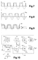
- the samples are taken at instants corresponding to edges of the second clock signal CK 90 , i.e., to the peak values (see Figure 8).
- the synchronization of the second clock signal CK 90 is ensured by the PLL circuit 113.
- the differentiator stage 110 amplifies the first reading voltages V RD1 , V RD2 and eliminates any possible intrinsic offset of the microstructure 102 or any offset introduced by the transimpedence amplifier 109.
- the elimination of the offset is particularly important for correct operation of the PLL circuit 113 and, consequently, of the controller 112.
- the comparator 116 switches at instants in which the phase of the first reading voltages V RD1 , V RD2 is not known and the phase-locking fails.
- the first and second clock signals CK, CK 90 do not contain useful information because their edges do not correspond to the changes of sign or to the peak values of the first reading voltages V RD1 , V RD2 .
- the differentiator stage 110 suppresses the offset, and hence the comparator 116 switches at significant instants for phase-locking.
- the first and second clock signals CK, CK 90 are synchronized to the first reading voltages V RD1 , V RD2 with zero and 90° phase lag, respectively.
- the controller 112, then, is correctly clocked.
- the use of the differentiator stage 110 is additionally advantageous because it enables amplification of the first reading voltages V RD1 , V RD2 without introducing phase offsets around the resonance frequency ⁇ R of the microstructure 102.
- the structure of the driving device 103 is far simpler than devices that use sigma-delta converters. Nevertheless, the oscillation frequency control is in any case accurate and is capable of rapidly compensating for any possible external disturbance.
- the reading device 104 comprises a charge amplifier 120, a first filter 121 and a second filter 122, which are included in the reading feedback loop 106, together with the sensing mass 108. Furthermore, the reading device 104 is provided with a demodulation stage 123, comprising a first demodulator 124 and a second demodulator 125 (mixers), with associated thereto respective post-demodulation filters 126, 127. All the components 120-127 that form the reading device 104 are of a discrete-time analog type and, in particular, are made up of fully differential switched-capacitor circuits. The electrical quantities used are then sampled, but not quantified. Thanks to the discrete-time operation, the reading device 14 can use a single pair of terminals 108c, 108d of the time-division sensing mass 108 both for reading, and for actuation.
- the charge amplifier 120 has inputs connected to the terminals 108c, 108d of the sensing mass 108 for receiving second reading currents I RS1 , I RS2 , which are correlated to the linear velocity of oscillation of the sensing mass 108 along the second axis Y.
- second reading voltages V RS1 , V RS2 indicative of the displacement of the sensing mass 108 along the second axis Y; also the second reading voltages V RS1 , V RS2 have equal amplitude and frequency and are out of phase by 180° with respect to one another.
- the first filter 121 and the second filter 122 are cascaded together, downstream of the charge amplifier 120.
- the first filter 121 has a transfer function C 1 (z) of a low-pass type and operates so as to obtain a stability condition on the magnitude of the gain of the reading feedback loop 106.
- a raw signal S RAW is present, which is correlated both to the instantaneous angular velocity of the microstructure 102, and to the spurious drawing motions.
- the second filter 122 has a transfer function C 2 (z) configured so as to recover the delays introduced by the first filter 121 and impose a stability condition on the phase of the gain of the reading feedback loop 106. Consequently, the transfer function C 1 (z) of the first filter 121 and the transfer function C 2 (z) of the second filter 122 ensure, in combination, the stability of the reading feedback loop 106.
- the second filter 122 operates by supplying to the terminals 108c, 108d of the sensing mass 108 reading feedback voltages V FBS1 , V FBS2 .
- the demodulation stage 123 is connected to the output of the first filter 121, to pick up the raw signal S RAW , which is supplied to the demodulators 124, 125. Note that the point of the reading feedback loop 106 from which the raw signal S RAW is picked up is the most favourable one as regards the signal-to-noise ratio.
- the first demodulator 124 has a demodulation input 124a connected to the driving device 103 for receiving the first clock signal CK
- the second demodulator 125 has a demodulation input 125a connected to the driving device 103 for receiving the second clock signal CK 90 .
- the outputs of the first and second post-demodulation filters 126, 127 form the first output 104a and the second output 104b, respectively, of the reading device 104.
- the sensing feedback loop 106 performs a negative force feedback on the sensing mass 108 of the inertial sensor 6.
- the reading device 104 In response to a displacement of the sensing mass 108 along the second axis Y, the reading device 104, by means of the reading feedback voltages V FBS1 , V FBS2 , applies electrostatic forces tending to bring the sensing mass 108 itself back into its rest position Y 0 .
- the raw signal S RAW is generated in the sensing feedback loop 106 and is correlated to the displacements of the sensing mass 108 along the second axis Y. Furthermore, the raw signal S RAW is amplitude-modulated in DSB-SC (Double Side Band - Suppressed Carrier) mode and is thus the sum of two components.
- a first component useful for measurement of the instantaneous angular velocity, is in phase with the displacement of the sensing mass 108 and has an amplitude correlated to the Coriolis acceleration (along the second axis Y) to which the sensing mass 108 itself is subject on account of the oscillation along the first axis X and of the rotation of the microstructure 102.
- a second component, 90° out of phase, is correlated to the spurious drawing motions. For example, if the driving mass 107 oscillates in a direction which is not perfectly aligned to the first axis X, the sensing mass 108 can be driven in oscillation along the second axis Y even in the absence of rotation of the microstructure 102.
- Both of the contributions have the same carrier frequency, i.e., the resonance frequency ⁇ R of the driving mass 107, but are 90° out of phase with respect to one another.
- the first contribution is in phase with the first clock signal CK
- the second contribution is in phase with the second clock signal CK 90 .
- the first output signal S OUT1 and the second output signal S OUT2 are generated using, respectively, the first clock signal CK and the second clock signal CK 90 for demodulating the raw signal S RAW .
- the first output signal S OUT1 corresponds to the first contribution, and hence its amplitude is correlated to the instantaneous angular velocity of the microstructure 102
- the second output signal S OUT2 corresponds to the second contribution, and its amplitude is correlated to the amount of the spurious drawing motions.
- the post-demodulation filters 126, 127 eliminate the frequency components 2 ⁇ R from the first and second output signals S OUT1 , S OUT2 after demodulation.
- the reading device 104 is advantageous because it enables a precise reading of the displacements of the sensing mass 108 to be obtained, thanks to the force feedback, using only analog circuits. For this reason, the reading device 104 is far simpler to produce, as compared to traditional feedback loops based upon sigma-delta modulators.
- the gyroscope 100 affords another advantage, which derives from the layout of the microstructure 102. Due to the location of the insulating regions 23, 24, in fact, the driving mass 107 and the sensing mass 108 can be biased independently of one another. In particular, it is possible to maintain the movable actuation electrodes 11 of the driving mass 107 connected to ground irrespective of the voltages that are supplied to the sensing mass 108 by the reading device 104 for exerting the force feedback.
- the invention can be advantageously exploited for producing electromechanical oscillators of any type, as already mentioned previously.
- the reading device according to the invention can be used in gyroscopes having microstructures different from the ones described herein.
- the driving mass and the sensing mass could be in direct electrical connection with one another, without any insulating regions.
Landscapes
- Engineering & Computer Science (AREA)
- Signal Processing (AREA)
- Physics & Mathematics (AREA)
- General Physics & Mathematics (AREA)
- Radar, Positioning & Navigation (AREA)
- Remote Sensing (AREA)
- Gyroscopes (AREA)
Abstract
Description
- The present invention relates to a resonant micro-electro-mechanical system with analog driving.
- As is known, the use of micro-electro-mechanical systems, or MEMS, is increasingly widespread in various sectors of technology and has yielded encouraging results especially in the construction of inertial sensors, micro-integrated gyroscopes, and electromechanical oscillators for a wide range of applications.
- MEMS systems of this type are usually based upon micro-electro-mechanical structures comprising at least one mass, which is connected to a fixed body (stator) by means of springs and is movable with respect to the stator according to predetermined degrees of freedom. The movable mass and the stator are capacitively coupled by a plurality of respective comb-fingered and mutually facing electrodes, so as to form capacitors. The movement of the movable mass with respect to the stator, for example on account of an external stress, modifies the capacitance of the capacitors; from this it is possible to trace back to the relative displacement of the movable mass with respect to the fixed body and hence to the applied force. Instead, by supplying appropriate biasing voltages, it is possible to apply an electrostatic force to the movable mass to set it in motion. Furthermore, to obtain electromechanical oscillators the frequency response of the inertial MEMS structures is exploited, which is typically of a second order low-pass type. By way of example, Figures 1 and 2 show the curve of the magnitude and of the phase of the transfer function between the force applied to the movable mass and its displacement with respect to the stator, in an inertial MEMS structure.
- Many MEMS systems (in particular, all electromechanical oscillators and gyroscopes) must envisage driving devices that have the task of maintaining the movable mass in oscillation.
- A first known type of solution envisages supplying, in open loop, periodic stresses on the resonance frequency of the MEMS structure. The solution is simple, but also far from effective because the resonance frequency is not known with precision on account of the uneliminable dispersions in the processes of micromachining of semiconductors. Furthermore, the resonance frequency of each individual device can vary over time, for example on account of temperature gradients or, more simply, on account of ageing.
- Then, feedback driving circuits have been proposed, which are based upon the use of sigma-delta modulators. Circuits of this type are undoubtedly more effective than the previous ones in stabilizing oscillation of the movable mass at the real resonance frequency and in suppressing any disturbance. However, different stages are necessary for filtering, decimating and further processing the bitstream supplied by the sigma-delta modulator. For this reason, currently available feedback driving circuits are complex to produce, cumbersome and, in practice, costly.
- The purpose of the present invention is to overcome the limitations described.
- According to the present invention a resonant micro-electro-mechanical system is provided, as defined in
claim 1. - For a better understanding of the invention, an embodiment thereof is now described, purely by way of non-limiting example and with reference to the attached drawings, in which:
- Figures 1 and 2 show graphs corresponding to the frequency response of a micro-electro-mechanical structure;
- Figure 3 is a simplified block diagram of a resonant micro-electro-mechanical system;
- Figure 4 is a plan view of a microstructure included in the system of Figure 3;
- Figure 4a is a simplified view of a part of the microstructure of Figure 4;
- Figure 5 is a more detailed block diagram of a part of the micro-electro-mechanical system of Figure 3, made according to the present invention;
- Figure 6 is a graph corresponding to the frequency response of an element of the block diagram of Figure 5;
- Figures 7-9 are graphs illustrating plots of quantities relating to the micro-electro-mechanical system of Figure 3; and
- Figure 10 is a more detailed block diagram of a part of the micro-electro-mechanical system of Figure 3.
- In the following description, reference will be made to the use of the invention in a micro-integrated gyroscope. This is not, however, to be considered in any way limiting, in so far as the invention can be exploited in all the cases where, in a micro-electro-mechanical structure, a movable mass must be excited and continuously maintained in oscillation at a natural resonance frequency. In particular, the invention can be advantageously applied to the construction of MEMS electromechanical oscillators.
- With reference to Figure 3, a
micro-integrated gyroscope 100 comprises amicrostructure 102, made using MEMS technology, adriving device 103, and areading device 104, housed on asupport 101. Themicrostructure 102, which will be illustrated in detail hereinafter, is provided with anactuation system 5 and with aninertial sensor 6, which includes respective movable masses. More precisely, theactuation system 5 comprises adriving mass 107, oscillating about a rest position according to a degree of freedom of its own, in particular along a first axis X. Theinertial sensor 6 has a detection axis directed according to a second axis Y, which is perpendicular to the first axis X, and comprises asensing mass 108, mechanically connected to thedriving mass 107 by springs (herein not illustrated) so as to be drawn in movement along the first axis X when thedriving mass 107 is excited. Furthermore, thesensing mass 108 is relatively movable with respect to thedriving mass 107 in the direction of the second axis Y and thus has a further degree of freedom. - The
driving device 103 and thereading device 104 are connected to themicrostructure 102 so as to form, respectively, adriving feedback loop 105, including thedriving mass 107, and areading feedback loop 106, including thesensing mass 108. Furthermore, thereading device 104 has a first output 104a and a second output 104b, which supply a first and, respectively, a second output signal SOUT1, SOUT2. In particular, the first output signal SOUT1 is correlated to the acceleration to which thesensing mass 108 is subjected along the second axis Y; and the second output signal SOUT2 is correlated to displacements of thesensing mass 108, once again in a direction of the second axis Y, on account of spurious drawing motions. - As is clarified in greater detail in the course of the ensuing description, the
driving device 103 exploits thedriving feedback loop 105 for maintaining thedriving mass 107 in self-oscillation along the first axis X at its resonance frequency ωR (for example, 4 kHz). Furthermore, thedriving device 103 generates a first clock signal CK and a second clock signal CK90, which is 90° out of phase, and supplies them to thereading device 104 for the purpose of synchronizing the operations of driving and reading of themicrostructure 102. - The
reading device 104 uses thereading feedback loop 106 to read the displacements of thesensing mass 108, which are determined by the resultant of the forces acting on thesensing mass 108 itself along the second axis Y. In practice, thesensing feedback loop 106 performs a force feedback for maintaining thesensing mass 108 in a rest position. The intensity of the electrostatic force to be applied is correlated to the displacement of thesensing mass 108 and hence to the forces acting thereon and can be estimated in a way in itself known, using the signals (voltages or currents) present in thesensing feedback loop 106. - The
gyroscope 100 operates in the following way. Thedriving mass 107 is set in oscillation along the first axis X and draws along in movement in the same direction also thesensing mass 108. Consequently, when themicrostructure 102 rotates about an axis perpendicular to the plane of the axes X, Y with a certain instantaneous angular velocity, thesensing mass 108 is subject to a Coriolis force, which is parallel to the second axis Y and is proportional to the instantaneous angular velocity of themicrostructure 102 and to the linear velocity of the twomasses 
where MS is the value of thesensing mass 108, Ω is the angular velocity of themicrostructure 102, and X' is the linear velocity of the twomasses - In effect, also the
driving mass 107 is subject to a Coriolis force; however, said force is countered by the constraints that impose on thedriving mass 107 a movement exclusively along the first axis X. - The Coriolis force and acceleration to which the
sensing mass 108 is subjected are measured by theinertial sensor 6. The response of theinertial sensor 6 can, however, contain also a component due to spurious drawing motions, which do not correspond to real rotations of themicrostructure 102 and are caused by imperfections in the constraints of thedriving mass 107 or in the mechanical coupling with thesensing mass 108. - In particular, the first output signal SOUT1 is correlated to the Coriolis force (and to the Coriolis acceleration) and hence also to the instantaneous angular velocity of the
microstructure 102; the second output signal SOUT2 is, instead, correlated to the spurious motions of drawing. Furthermore, the first output signal SOUT1 is modulated in amplitude proportionally to the Coriolis force and, consequently, to the instantaneous angular velocity of themicrostructure 102, with the carrier centred at the resonance frequency ωR. The frequency band associated to the modulating quantity, i.e., the instantaneous angular velocity, is however, far lower than the resonance frequency ωR (for example, 10 Hz). - Figure 4 shows the complete layout of the
microstructure 102, which is of the general type described in the European patent application No. EP-A-1 253 399. Themicrostructure 102 is made up of twoparts central springs 3, arranged symmetrically with respect to a barycentric axis designated by B and parallel to the first axis X. Designated by X0 and Y0 in Figure 4a are a rest position of thedriving mass 107 with respect to the first axis X and, respectively, a rest position of thesensing mass 108 with respect to the second axis Y. - Each
part respective actuation system 5, a respectiveinertial sensor 6, and amechanical connection 7, which connects theactuation system 5 to theinertial sensor 6. In Figure 3, themicrostructure 102 has been represented schematically in a simplified way with reference to just one of the twoparts - In detail, the
actuation system 5 comprises thedriving mass 107 having an open concave shape (C shape),movable actuation electrodes 11 connected to thedriving mass 107, and first and second fixedactuation electrodes movable actuation electrodes 11. Thedriving mass 107 is supported by first andsecond anchorages second anchoring springs driving mass 107 in the proximity of the outer edges of thedriving mass 107 itself. - The
inertial sensor 6 comprises thesensing mass 108 andmovable sensing electrodes 21 comb-fingered to first and second fixedsensing electrodes sensing mass 108 is surrounded on three sides by thedriving mass 107 and is supported thereby through twofirst coupling springs 25a and twosecond coupling springs 25b. The coupling springs 25a, 25b constitute themechanical connection 7 and are connected to thesensing mass 108 in the proximity of the edges thereof. Themovable sensing electrodes 21 extend from thesensing mass 108 from the side thereof not facing thedriving mass 107. - The
sensing mass 108 is divided into afirst part 108a and asecond part 108b by a firstinsulating region 23; likewise, the drivingmass 107 is divided into amain portion 107a and twoend portions 107b by two second insulatingregions 24. - In detail, the first
insulating region 23 extends approximately parallel to the central axis of symmetry A so that thefirst part 108a of thesensing mass 108 is supported and connected to the drivingmass 107 only via thefirst coupling springs 25a, whilst thesecond part 108b of thesensing mass 108 is supported and connected to the drivingmass 107 only via the second coupling springs 25b. - Furthermore, the second insulating
regions 24 extend transversely to the respective C-shaped arms so that themain portion 107a of the drivingmass 107 is connected only to the first coupling springs 25a and to the first anchoring springs 16a, whilst theend parts 107b of the drivingmass 107 is connected only to the second coupling springs 25b and to the second anchoring springs 16b. The position of the second insulatingregions 24 is moreover such that themovable actuation electrodes 11 extend from themain portion 107a of the drivingmass 107 and are electrically connected thereto. -
Actuation biasing regions 27, of a buried type, are connected to thefirst anchoring regions 15a; firstdetection biasing regions 28, which are also of a buried type, are connected to thesecond anchoring regions 15b; seconddetection biasing regions 29 are connected to the firstfixed sensing electrodes 22a; and thirddetection biasing regions 30 are connected to the secondfixed sensing electrodes 22b. - In this way, the
first part 108a of thesensing mass 108, thefirst coupling springs 25a, themain portion 107a of the drivingmass 107, themovable actuation electrodes 11, the first anchoring springs 16a, and thefirst anchoring regions 15a are all biased at the same potential, which is applied via theactuation biasing regions 27, and are electrically insulated, via the insulatingregions second part 108b of thesensing mass 108, the second coupling springs 25b, theend portions 107b of the drivingmass 107, the second anchoring springs 16b, and thesecond anchoring regions 15b, biased via the firstdetection biasing regions 28. - With reference to Figure 5, the driving
device 103 comprises atransimpedence amplifier 109, adifferentiator stage 110, a variable-gain amplifier (VGA)circuit 111, acontroller 112, and a phase-locked-loop (PLL)circuit 113. - The
transimpedence amplifier 109 is of a fully differential type and has a pair of inputs connected to readingoutputs actuation system 5 for receiving first reading currents IRD1, IRD2, which are correlated to the linear velocity of oscillation of the drivingmass 107 along the first axis X. On the outputs of thetransimpedence amplifier 109 there are hence first reading voltages VRD1, VRD2, which also indicate the linear velocity of oscillation of the drivingmass 107 along the first axis X. Also the first reading voltages VRD1, VRD2 have equal amplitude and frequency and are out of phase by 180°. - The
differentiator stage 110 is cascaded to thetransimpedence amplifier 109. The transfer function of thedifferentiator stage 110, which is of a high-pass type and has a zero at zero frequency and a pole at a frequency ωP smaller than the resonance frequency ωR of themicrostructure 102, is of the type:
where s is a complex variable, K is a constant coefficient, and TP = 1/ωP is the time constant associated to the pole of the differentiator stage 110 (see also Figure 6). Preferably, the coefficient K is such that, for frequencies greater than the frequency ωP of the pole, the gain K/TP of thedifferentiator stage 110 is greater than unity. In practice then, thedifferentiator stage 110 amplifies the harmonic components of the first reading voltages VRD1, URD2 close to the resonance frequency ωR, whilst possible constant components are eliminated (for example offset voltages). Furthermore, in the bandpass B of thedifferentiator 110, i.e., for frequencies greater than the frequency ωP of the pole, the offset introduced by thedifferentiator stage 110 is substantially zero, since the contributions of the pole and of the zero are compensated. - The
VGA circuit 111 is connected between thedifferentiator stage 110 andactuation inputs mass 107 and supplies driving feedback voltages VFBD1, VFBD2 having amplitude and phase such as to maintain the drivingmass 107 in oscillation at the resonance frequency ωR. In particular, the amplitude of the driving feedback voltages VFBD1, VFBD2 depends upon the gain of theVGA circuit 111, which is determined by thecontroller 112 so that the global gain of the drivingfeedback loop 105 is a unit gain. - The
controller 112 is preferably of a switched-capacitor PID type and has first inputs 112a connected to the outputs of thedifferentiator stage 110, for receiving the first reading voltages VRD1, VRD2, amplified and depurated of the continuous component. A second input 112b of thecontroller 112 is connected to avoltage generator 115, supplying a reference voltage VREF. Thecontroller 112 moreover has an output, which is connected to a control input 111a of theVGA circuit 111 and supplies a control voltage VC. In practice, thecontroller 112 generates the control voltage VC on the basis of the difference between the voltages on the first inputs 112a and the reference voltage VREF. Preferably, the gain of theVGA circuit 111 depends linearly upon the control voltage VC. - The
PLL circuit 113 has inputs connected to the outputs of thedifferentiator stage 110 through acomparator 116, of an analog type with hysteresis, and anoutput 113a, connected to a clock input 112c of thecontroller 112. Thecomparator 116 supplies at output to thePLL circuit 113, the first clock signal CK, which is a square-wave voltage having a first value in a first half-period, in which the voltages on the outputs of thedifferentiator stage 110 have a respective sign, and a second value in a second half-period, in which the voltages on the outputs of thedifferentiator stage 110 have a sign opposite to that of the first half-period. In practice, the first clock signal switches at each change of sign of the first reading voltages VRD1, VRD2, which are in phase with the voltages on the outputs of thedifferentiator 110. Hysteresis prevents repeated switchings due to noise in the proximity of the changes of sign of the voltages on the outputs of thedifferentiator stage 110. Moreover, thePLL circuit 113 supplies the second clock signal CK90 on theoutput 113a. In particular (see Figures 7 and 8), the first clock signal CK has edges synchronized with instants of zero-crossing of the first reading voltages VRD1, VRD2 (one of which is represented with a dashed line). The second clock signal CK90 is 90° out of phase with respect to the first clock signal CK and is in phase with the peak values of the first reading voltages VRD1, VRD2. In other words, the first clock signal CK and the second clock signal CK90 are in phase, respectively, with the linear velocity and with the displacement of the drivingmass 107 along the first axis X. - The output of the
comparator 116 and theoutput 113a of thePLL circuit 113 are moreover connected to thereading device 104. - As previously mentioned, the driving
device 103 operates on the overall gain and phase of the drivingfeedback loop 105 so as to maintain the drivingmass 107 constantly in oscillation at the resonance frequency ωR. Thecontroller 112 intervenes above all upon triggering of the oscillation by increasing the gain of theVGA circuit 111, which is then reduced so that the overall gain of the drivingfeedback loop 105 is substantially a unit gain. In the second place, thecontroller 112 prevents - following upon external stresses, such as shocks or vibrations - the oscillations of themicrostructure 102 from degenerating into limit cycles. In the absence of thecontroller 112, in fact, the response of themicrostructure 102 can depart from the linearity domain, and hence uncontrolled oscillating motions may be set up. The effect of the external stresses is, instead, limited by thecontroller 112, which temporarily reduces the gain of theVGA circuit 111. Finally, the action of thecontroller 112 enables compensation of variations with respect to the nominal value and possible drift of the resonance frequency ωR. - The
controller 112 uses the second clock signal CK90 for consistently sampling the voltages on the outputs of thedifferentiator stage 110, always with the same phase. Preferably, the samples are taken at instants corresponding to edges of the second clock signal CK90, i.e., to the peak values (see Figure 8). As already explained, the synchronization of the second clock signal CK90 is ensured by thePLL circuit 113. - The
differentiator stage 110 amplifies the first reading voltages VRD1, VRD2 and eliminates any possible intrinsic offset of themicrostructure 102 or any offset introduced by thetransimpedence amplifier 109. The elimination of the offset is particularly important for correct operation of thePLL circuit 113 and, consequently, of thecontroller 112. As illustrated in Figure 9, when an offset OS is present, the first reading voltages VRD1, VRD2 do not change sign at each half-period, but at different instants. Consequently, thecomparator 116 switches at instants in which the phase of the first reading voltages VRD1, VRD2 is not known and the phase-locking fails. Thus, the first and second clock signals CK, CK90 do not contain useful information because their edges do not correspond to the changes of sign or to the peak values of the first reading voltages VRD1, VRD2. Instead, thedifferentiator stage 110 suppresses the offset, and hence thecomparator 116 switches at significant instants for phase-locking. For this reason, the first and second clock signals CK, CK90 are synchronized to the first reading voltages VRD1, VRD2 with zero and 90° phase lag, respectively. Also thecontroller 112, then, is correctly clocked. The use of thedifferentiator stage 110 is additionally advantageous because it enables amplification of the first reading voltages VRD1, VRD2 without introducing phase offsets around the resonance frequency ωR of themicrostructure 102. - On the whole, the structure of the
driving device 103 is far simpler than devices that use sigma-delta converters. Nevertheless, the oscillation frequency control is in any case accurate and is capable of rapidly compensating for any possible external disturbance. - With reference to Figure 10, the
reading device 104 comprises acharge amplifier 120, afirst filter 121 and asecond filter 122, which are included in the readingfeedback loop 106, together with thesensing mass 108. Furthermore, thereading device 104 is provided with a demodulation stage 123, comprising afirst demodulator 124 and a second demodulator 125 (mixers), with associated thereto respectivepost-demodulation filters reading device 104 are of a discrete-time analog type and, in particular, are made up of fully differential switched-capacitor circuits. The electrical quantities used are then sampled, but not quantified. Thanks to the discrete-time operation, the reading device 14 can use a single pair ofterminals division sensing mass 108 both for reading, and for actuation. - The
charge amplifier 120 has inputs connected to theterminals sensing mass 108 for receiving second reading currents IRS1, IRS2, which are correlated to the linear velocity of oscillation of thesensing mass 108 along the second axis Y. On account of the charge amplification, on the outputs of thecharge amplifier 120 there are second reading voltages VRS1, VRS2, indicative of the displacement of thesensing mass 108 along the second axis Y; also the second reading voltages VRS1, VRS2 have equal amplitude and frequency and are out of phase by 180° with respect to one another. - The
first filter 121 and thesecond filter 122 are cascaded together, downstream of thecharge amplifier 120. In greater detail, thefirst filter 121 has a transfer function C1(z) of a low-pass type and operates so as to obtain a stability condition on the magnitude of the gain of the readingfeedback loop 106. On the outputs of the first filter 121 a raw signal SRAW is present, which is correlated both to the instantaneous angular velocity of themicrostructure 102, and to the spurious drawing motions. - The
second filter 122 has a transfer function C2(z) configured so as to recover the delays introduced by thefirst filter 121 and impose a stability condition on the phase of the gain of the readingfeedback loop 106. Consequently, the transfer function C1(z) of thefirst filter 121 and the transfer function C2(z) of thesecond filter 122 ensure, in combination, the stability of the readingfeedback loop 106. In practice, thesecond filter 122 operates by supplying to theterminals sensing mass 108 reading feedback voltages VFBS1, VFBS2. - The demodulation stage 123 is connected to the output of the
first filter 121, to pick up the raw signal SRAW, which is supplied to thedemodulators feedback loop 106 from which the raw signal SRAW is picked up is the most favourable one as regards the signal-to-noise ratio. Thefirst demodulator 124 has a demodulation input 124a connected to thedriving device 103 for receiving the first clock signal CK, and thesecond demodulator 125 has a demodulation input 125a connected to thedriving device 103 for receiving the second clock signal CK90. The outputs of the first and secondpost-demodulation filters reading device 104. - As previously mentioned, the
sensing feedback loop 106 performs a negative force feedback on thesensing mass 108 of theinertial sensor 6. In response to a displacement of thesensing mass 108 along the second axis Y, thereading device 104, by means of the reading feedback voltages VFBS1, VFBS2, applies electrostatic forces tending to bring thesensing mass 108 itself back into its rest position Y0. - The raw signal SRAW is generated in the
sensing feedback loop 106 and is correlated to the displacements of thesensing mass 108 along the second axis Y. Furthermore, the raw signal SRAW is amplitude-modulated in DSB-SC (Double Side Band - Suppressed Carrier) mode and is thus the sum of two components. A first component, useful for measurement of the instantaneous angular velocity, is in phase with the displacement of thesensing mass 108 and has an amplitude correlated to the Coriolis acceleration (along the second axis Y) to which thesensing mass 108 itself is subject on account of the oscillation along the first axis X and of the rotation of themicrostructure 102. A second component, 90° out of phase, is correlated to the spurious drawing motions. For example, if the drivingmass 107 oscillates in a direction which is not perfectly aligned to the first axis X, thesensing mass 108 can be driven in oscillation along the second axis Y even in the absence of rotation of themicrostructure 102. - Both of the contributions have the same carrier frequency, i.e., the resonance frequency ωR of the driving
mass 107, but are 90° out of phase with respect to one another. In particular, the first contribution is in phase with the first clock signal CK, whereas the second contribution is in phase with the second clock signal CK90. - The first output signal SOUT1 and the second output signal SOUT2 are generated using, respectively, the first clock signal CK and the second clock signal CK90 for demodulating the raw signal SRAW. For this reason, the first output signal SOUT1 corresponds to the first contribution, and hence its amplitude is correlated to the instantaneous angular velocity of the
microstructure 102, and the second output signal SOUT2 corresponds to the second contribution, and its amplitude is correlated to the amount of the spurious drawing motions. - The post-demodulation filters 126, 127 eliminate the frequency components 2ωR from the first and second output signals SOUT1, SOUT2 after demodulation.
- The
reading device 104 is advantageous because it enables a precise reading of the displacements of thesensing mass 108 to be obtained, thanks to the force feedback, using only analog circuits. For this reason, thereading device 104 is far simpler to produce, as compared to traditional feedback loops based upon sigma-delta modulators. - The
gyroscope 100 affords another advantage, which derives from the layout of themicrostructure 102. Due to the location of the insulatingregions mass 107 and thesensing mass 108 can be biased independently of one another. In particular, it is possible to maintain themovable actuation electrodes 11 of the drivingmass 107 connected to ground irrespective of the voltages that are supplied to thesensing mass 108 by thereading device 104 for exerting the force feedback. - Finally, it is evident that modifications and variations can be made to the resonant micro-electro-mechanical system described herein, without thereby departing from the scope of the present invention, as defined in the annexed claims.
- In particular, the invention can be advantageously exploited for producing electromechanical oscillators of any type, as already mentioned previously. In addition, the reading device according to the invention can be used in gyroscopes having microstructures different from the ones described herein. For instance, the driving mass and the sensing mass could be in direct electrical connection with one another, without any insulating regions. In this case, however, it is preferable to associate to the transimpedence amplifier an offset-compensation stage. Alternatively, it is also possible to use a single mass with actuation and detection systems for two independent axes.
Claims (15)
- A resonant micro-electro-mechanical system comprising a microstructure (102), having a mass (107), which is free to oscillate in accordance with a predetermined degree of freedom (X), and a driving device (103), coupled to said mass (107) for maintaining said mass (107) in oscillation at a resonance frequency (ωR), wherein said driving device (103) comprises a differential sense amplifier (109), supplying first signals (VRD1, VRD2) indicative of a velocity of oscillation of said mass (107), and an actuation and control stage (111, 112, 113, 116) supplying second signals (VFBD1, VFBD2) for driving said mass (107) on the basis of said first signals (VRD1, VRD2);
characterized in that said driving device (103) comprises filtering means (110) of a high-pass type, which is connected between said differential sense amplifier (109) and said actuation and control stage (111, 112, 113, 116) and has a bandpass (B) including said resonance frequency (ωR). - The micro-electro-mechanical system according to claim 1, wherein said filtering means (110) is of a zero phase-lag type.
- The micro-electro-mechanical system according to claim 1 or 2, wherein said filtering means (110) has a gain greater than 1 in said bandpass (B).
- The micro-electro-mechanical system according to any one of the preceding claims, wherein said filtering means (110) comprises a differentiator.
- The micro-electro-mechanical system according to any one of the preceding claims, wherein said differential sense amplifier (109) and said actuation and control stage (111, 112, 113, 116) comprise components made up of switched-capacitor circuits.
- The micro-electro-mechanical system according to any one of the preceding claims, wherein said differential sense amplifier (109), said filtering means (110), and said actuation and control stage (111, 112, 113, 116) are connected so as to form an oscillating feedback loop (105), including said mass (107).
- The micro-electro-mechanical system according to claim 6, wherein said actuation and control stage (111, 112, 113, 116) comprises a variable-gain amplifier (111) and a controller (112), for controlling a gain (A) of said variable-gain amplifier (111) so that said feedback loop (105) has unit gain.
- The micro-electro-mechanical system according to claim 7, wherein said driving device (103) comprises a synchronization circuit (113, 116) associated to said controller (112) for clocking said controller (112) on the basis of said first signals (VRD1, URD2).
- The micro-electro-mechanical system according to claim 8, wherein said synchronization circuit (113, 116) comprises a PLL circuit (113).
- The micro-electro-mechanical system according to claim 9, wherein said synchronization circuit (113) comprises a comparator (116) having inputs connected to outputs of said filtering means (110) and an output connected to said PLL circuit (113) for supplying a first clock signal (CK) in the form of a square-wave voltage having a first value in a first half-period, in which voltages on said outputs of said filtering means (110) have a respective sign, and a second value in a second half-period, in which said voltages on said outputs of said filtering means (110) have a sign opposite to that of the first half-period.
- The micro-electro-mechanical system according to claim 10, wherein said PLL circuit (113) has an output connected to a clock input (112c) of said controller (112) for supplying a second clock signal (CK90) 90° out of phase with respect to said first clock signal (CK).
- An integrated micro-electro-mechanical gyroscope, comprising:- a microstructure (102), having a first mass (107), which is free to oscillate along a first axis (X); and a driving device (103), coupled to said first mass (107) for maintaining said first mass (107) in oscillation at a resonance frequency (ωR), wherein said driving device (103) comprises a differential sense amplifier (109), supplying first signals (VRD1, URD2) indicative of a velocity of oscillation of said first mass (107), and an actuation and control stage (111, 112, 113, 116) supplying second signals (VFBD1, VFBD2) for driving said first mass (107) on the basis of said first signals (VRD1, VRD2); and- inertial sensor means (6, 104, 106), which is mechanically coupled to said first mass (107) so as to be fixedly drawn along by said first mass (107) along said first axis (X) and has an axis of detection (Y) perpendicular to said first axis (X) ;
characterized in that said driving device (103) comprises filtering means (110) of a high-pass type, which is connected between said differential sense amplifier (109) and said actuation and control stage (111, 112, 113, 116) and has a bandpass (B) including said resonance frequency (ωR). - The gyroscope according to claim 12, wherein said inertial sensor means (6, 104, 106) comprise:- a second mass (108), which is relatively movable with respect to said first mass (107) along said axis of detection (Y) and with respect to a rest position (Y0); and- displacement-detection means (104, 106) for detecting a displacement of said second mass (108) along said second axis (Y), in which said displacement-detection means (104, 106) include a force feedback loop (106) supplying electrostatic forces tending to bring back said second mass (108) into said rest position (Y0) in response to a displacement of said mass (108) along said second axis (Y).
- The gyroscope according to claim 13, wherein said force feedback loop (106) is of a purely analog type.
- The gyroscope according to any one of claims 12 to 15, wherein said inertial sensor means (6, 104, 106) comprise a micro-electro-mechanical inertial sensor (106).
Priority Applications (2)
| Application Number | Priority Date | Filing Date | Title |
|---|---|---|---|
| EP04425599.0A EP1624285B1 (en) | 2004-08-03 | 2004-08-03 | Resonant micro-electro-mechanical system and gyroscope |
| US11/195,347 US7305880B2 (en) | 2004-08-03 | 2005-08-02 | Resonant micro-electro-mechanical system with analog driving |
Applications Claiming Priority (1)
| Application Number | Priority Date | Filing Date | Title |
|---|---|---|---|
| EP04425599.0A EP1624285B1 (en) | 2004-08-03 | 2004-08-03 | Resonant micro-electro-mechanical system and gyroscope |
Publications (2)
| Publication Number | Publication Date |
|---|---|
| EP1624285A1 true EP1624285A1 (en) | 2006-02-08 |
| EP1624285B1 EP1624285B1 (en) | 2014-07-23 |
Family
ID=34932695
Family Applications (1)
| Application Number | Title | Priority Date | Filing Date |
|---|---|---|---|
| EP04425599.0A Expired - Lifetime EP1624285B1 (en) | 2004-08-03 | 2004-08-03 | Resonant micro-electro-mechanical system and gyroscope |
Country Status (2)
| Country | Link |
|---|---|
| US (1) | US7305880B2 (en) |
| EP (1) | EP1624285B1 (en) |
Cited By (5)
| Publication number | Priority date | Publication date | Assignee | Title |
|---|---|---|---|---|
| ITTO20090420A1 (en) * | 2009-06-03 | 2010-12-04 | St Microelectronics Srl | MICROELETTROMECHANICAL GYROSCOPE WITH POSITION CONTROL AND METHOD FOR THE CONTROL OF A MICROELECTRANOMANICAL GYROSCOPE |
| EP2360449A1 (en) | 2010-02-16 | 2011-08-24 | STMicroelectronics S.r.l. | Microelectromechanical gyrospcope with inversion of actuation forces, and method for actuating a microelectromechanical gyroscope |
| EP2360448A1 (en) | 2010-02-15 | 2011-08-24 | STMicroelectronics Srl | Microelectromechanical gyroscope with calibrated synchronization of actuation and method for actuating a microelectromechanical gyroscope |
| US9551576B2 (en) | 2011-11-23 | 2017-01-24 | Cambridge Enterprise Limited | MEMS inertial sensor and method of inertial sensing |
| US10088333B2 (en) | 2013-07-30 | 2018-10-02 | Stmicroelectronics S.R.L. | Method and system for gyroscope real-time calibration |
Families Citing this family (43)
| Publication number | Priority date | Publication date | Assignee | Title |
|---|---|---|---|---|
| EP1624286B1 (en) * | 2004-08-03 | 2017-10-04 | STMicroelectronics Srl | Micro-electro-mechanical sensor with force feedback loop |
| DE102005003630A1 (en) * | 2005-01-26 | 2006-07-27 | Robert Bosch Gmbh | Electromechanical delta-sigma-modulator for e.g. airbag control system of motor vehicle, has multibit-DAC to adjust amplification in servo loop and bandwidth of modulator independent of input signal of multibit-ADC |
| US7669475B2 (en) * | 2006-09-28 | 2010-03-02 | Rosemount Aerospace Inc. | System and method for measuring rotational movement about an axis |
| DE102006055589B4 (en) * | 2006-11-24 | 2012-07-19 | Infineon Technologies Ag | Measuring device and measured value sensor with coupled processing and excitation frequency |
| EP1962054B1 (en) * | 2007-02-13 | 2011-07-20 | STMicroelectronics Srl | Microelectromechanical gyroscope with open loop reading device and control method of a microelectromechanical gyroscope |
| DE102008044664B4 (en) | 2008-08-28 | 2023-12-21 | Continental Automotive Technologies GmbH | Method for frequency control of an oscillator arrangement |
| US8076893B2 (en) * | 2008-09-04 | 2011-12-13 | The Board Of Trustees Of The University Of Illinois | Displacement actuation and sensing for an electrostatic drive |
| US7859352B2 (en) * | 2008-10-15 | 2010-12-28 | Honeywell International Inc. | Systems and methods to overcome DC offsets in amplifiers used to start resonant micro-electro mechanical systems |
| US8183944B2 (en) * | 2009-04-03 | 2012-05-22 | Invensense, Inc. | Method and system for using a MEMS structure as a timing source |
| ITTO20090334A1 (en) * | 2009-04-28 | 2010-10-29 | St Microelectronics Srl | DEVICE AND METHOD OF PROTECTION FROM DISTURBANCES FOR A DIGITAL SIGNAL |
| US8739626B2 (en) | 2009-08-04 | 2014-06-03 | Fairchild Semiconductor Corporation | Micromachined inertial sensor devices |
| EP2336717B1 (en) | 2009-12-21 | 2012-09-19 | STMicroelectronics Srl | Microelectromechanical device having an oscillating mass, and method for controlling a microelectromechanical device having an oscillating mass |
| TWI411766B (en) * | 2010-04-27 | 2013-10-11 | Univ Nat Chiao Tung | Uniaxial Control Input Gyroscope System with Flaw Compensation. |
| WO2012037540A2 (en) | 2010-09-18 | 2012-03-22 | Fairchild Semiconductor Corporation | Micromachined monolithic 3-axis gyroscope with single drive |
| WO2012037536A2 (en) | 2010-09-18 | 2012-03-22 | Fairchild Semiconductor Corporation | Packaging to reduce stress on microelectromechanical systems |
| EP2616771B8 (en) | 2010-09-18 | 2018-12-19 | Fairchild Semiconductor Corporation | Micromachined monolithic 6-axis inertial sensor |
| US9278845B2 (en) | 2010-09-18 | 2016-03-08 | Fairchild Semiconductor Corporation | MEMS multi-axis gyroscope Z-axis electrode structure |
| EP2616389B1 (en) | 2010-09-18 | 2017-04-05 | Fairchild Semiconductor Corporation | Multi-die mems package |
| KR101443730B1 (en) | 2010-09-18 | 2014-09-23 | 페어차일드 세미컨덕터 코포레이션 | A microelectromechanical die, and a method for making a low-quadrature-error suspension |
| WO2012040245A2 (en) | 2010-09-20 | 2012-03-29 | Fairchild Semiconductor Corporation | Through silicon via with reduced shunt capacitance |
| CN103221795B (en) | 2010-09-20 | 2015-03-11 | 快捷半导体公司 | Microelectromechanical pressure sensor including reference capacitor |
| ITTO20110685A1 (en) * | 2011-07-28 | 2013-01-29 | St Microelectronics Srl | MICROELETTROMECHANICAL GYROSCOPE WITH PERFECT READING STAGE, AND METHOD |
| US8373465B1 (en) * | 2011-11-17 | 2013-02-12 | Texas Instruments Deutschland Gmbh | Electronic device and method for phase locked loop |
| US9062972B2 (en) | 2012-01-31 | 2015-06-23 | Fairchild Semiconductor Corporation | MEMS multi-axis accelerometer electrode structure |
| US8978475B2 (en) | 2012-02-01 | 2015-03-17 | Fairchild Semiconductor Corporation | MEMS proof mass with split z-axis portions |
| US8754694B2 (en) | 2012-04-03 | 2014-06-17 | Fairchild Semiconductor Corporation | Accurate ninety-degree phase shifter |
| US8742964B2 (en) | 2012-04-04 | 2014-06-03 | Fairchild Semiconductor Corporation | Noise reduction method with chopping for a merged MEMS accelerometer sensor |
| US9488693B2 (en) | 2012-04-04 | 2016-11-08 | Fairchild Semiconductor Corporation | Self test of MEMS accelerometer with ASICS integrated capacitors |
| EP2648334B1 (en) * | 2012-04-05 | 2020-06-10 | Fairchild Semiconductor Corporation | Mems device front-end charge amplifier |
| EP2647952B1 (en) | 2012-04-05 | 2017-11-15 | Fairchild Semiconductor Corporation | Mems device automatic-gain control loop for mechanical amplitude drive |
| US9069006B2 (en) | 2012-04-05 | 2015-06-30 | Fairchild Semiconductor Corporation | Self test of MEMS gyroscope with ASICs integrated capacitors |
| EP2647955B8 (en) | 2012-04-05 | 2018-12-19 | Fairchild Semiconductor Corporation | MEMS device quadrature phase shift cancellation |
| US9625272B2 (en) | 2012-04-12 | 2017-04-18 | Fairchild Semiconductor Corporation | MEMS quadrature cancellation and signal demodulation |
| KR101999745B1 (en) * | 2012-04-12 | 2019-10-01 | 페어차일드 세미컨덕터 코포레이션 | Micro-electro-mechanical-system(mems) driver |
| DE102013014881B4 (en) | 2012-09-12 | 2023-05-04 | Fairchild Semiconductor Corporation | Enhanced silicon via with multi-material fill |
| US9146109B2 (en) | 2012-11-26 | 2015-09-29 | Stmicroelectronics S.R.L. | Microelectromechanical gyroscope with improved start-up phase, system including the microelectromechanical gyroscope, and method for speeding-up the start up phase |
| ITTO20130013A1 (en) | 2013-01-09 | 2014-07-10 | St Microelectronics Srl | MICROELETTROMECHANICAL GYROSCOPE WITH COMPENSATION OF SQUARE SIGNAL COMPONENTS AND METHOD OF CONTROL OF A MICROELECTRANOMIC GYROSCOPE |
| US9644963B2 (en) | 2013-03-15 | 2017-05-09 | Fairchild Semiconductor Corporation | Apparatus and methods for PLL-based gyroscope gain control, quadrature cancellation and demodulation |
| US9835647B2 (en) | 2014-03-18 | 2017-12-05 | Fairchild Semiconductor Corporation | Apparatus and method for extending analog front end sense range of a high-Q MEMS sensor |
| CN106066175B (en) | 2015-04-24 | 2019-09-24 | 意法半导体股份有限公司 | Method for sensing the micro-electro-mechanical gyroscope of angular speed and sensing angular speed |
| US10622945B1 (en) * | 2017-07-26 | 2020-04-14 | Sitime Corporation | Low Allan-Deviation oscillator |
| EP3699610B1 (en) * | 2019-02-22 | 2023-04-19 | NXP USA, Inc. | Capacitance-to-voltage interface circuit |
| FR3108897B1 (en) * | 2020-04-03 | 2022-04-08 | Commissariat Energie Atomique | Sensor control method |
Citations (4)
| Publication number | Priority date | Publication date | Assignee | Title |
|---|---|---|---|---|
| US5627318A (en) * | 1992-08-21 | 1997-05-06 | Nippondenso Co., Ltd. | Mechanical force sensing semiconductor device |
| US5719460A (en) * | 1994-11-28 | 1998-02-17 | Nippondenso Co., Ltd | Angular velocity sensor |
| US20010037683A1 (en) * | 1995-05-30 | 2001-11-08 | Toshiyuki Nozoe | Angular velocity sensor |
| EP1296114A1 (en) * | 2001-02-19 | 2003-03-26 | Matsushita Electric Industrial Co., Ltd. | Angular velocity sensor and method of adjusting characteristics of the sensor |
Family Cites Families (9)
| Publication number | Priority date | Publication date | Assignee | Title |
|---|---|---|---|---|
| GB2329471B (en) | 1997-09-18 | 2001-08-15 | British Aerospace | A digital control system for a vibrating structure gyroscope |
| US6253612B1 (en) * | 1998-06-05 | 2001-07-03 | Integrated Micro Instruments, Inc. | Generation of mechanical oscillation applicable to vibratory rate gyroscopes |
| DE60120921T2 (en) * | 2001-04-27 | 2007-02-01 | Stmicroelectronics S.R.L., Agrate Brianza | Integrated gyro made of semiconductor material |
| US6792792B2 (en) * | 2001-06-04 | 2004-09-21 | Kelsey-Hayes Company | Diagnostic test for a resonant micro electro mechanical system |
| US6701786B2 (en) * | 2002-04-29 | 2004-03-09 | L-3 Communications Corporation | Closed loop analog gyro rate sensor |
| US6823733B2 (en) * | 2002-11-04 | 2004-11-30 | Matsushita Electric Industrial Co., Ltd. | Z-axis vibration gyroscope |
| GB0227084D0 (en) | 2002-11-20 | 2002-12-24 | Bae Systems Plc | Method and apparatus for measuring scalefactor variation in a vibrating structure gyroscope |
| US6934665B2 (en) * | 2003-10-22 | 2005-08-23 | Motorola, Inc. | Electronic sensor with signal conditioning |
| EP1624286B1 (en) * | 2004-08-03 | 2017-10-04 | STMicroelectronics Srl | Micro-electro-mechanical sensor with force feedback loop |
-
2004
- 2004-08-03 EP EP04425599.0A patent/EP1624285B1/en not_active Expired - Lifetime
-
2005
- 2005-08-02 US US11/195,347 patent/US7305880B2/en active Active
Patent Citations (4)
| Publication number | Priority date | Publication date | Assignee | Title |
|---|---|---|---|---|
| US5627318A (en) * | 1992-08-21 | 1997-05-06 | Nippondenso Co., Ltd. | Mechanical force sensing semiconductor device |
| US5719460A (en) * | 1994-11-28 | 1998-02-17 | Nippondenso Co., Ltd | Angular velocity sensor |
| US20010037683A1 (en) * | 1995-05-30 | 2001-11-08 | Toshiyuki Nozoe | Angular velocity sensor |
| EP1296114A1 (en) * | 2001-02-19 | 2003-03-26 | Matsushita Electric Industrial Co., Ltd. | Angular velocity sensor and method of adjusting characteristics of the sensor |
Cited By (8)
| Publication number | Priority date | Publication date | Assignee | Title |
|---|---|---|---|---|
| ITTO20090420A1 (en) * | 2009-06-03 | 2010-12-04 | St Microelectronics Srl | MICROELETTROMECHANICAL GYROSCOPE WITH POSITION CONTROL AND METHOD FOR THE CONTROL OF A MICROELECTRANOMANICAL GYROSCOPE |
| EP2259019A1 (en) | 2009-06-03 | 2010-12-08 | STMicroelectronics S.r.l. | Microelectromechanical gyroscope with position control driving and method for controlling a microelectromechanical gyroscope |
| EP2360448A1 (en) | 2010-02-15 | 2011-08-24 | STMicroelectronics Srl | Microelectromechanical gyroscope with calibrated synchronization of actuation and method for actuating a microelectromechanical gyroscope |
| EP2360449A1 (en) | 2010-02-16 | 2011-08-24 | STMicroelectronics S.r.l. | Microelectromechanical gyrospcope with inversion of actuation forces, and method for actuating a microelectromechanical gyroscope |
| CN102230800A (en) * | 2010-02-16 | 2011-11-02 | 意法半导体股份有限公司 | Microelectromechanical gyrospcope with inversion of actuation forces, and method for actuating a microelectromechanical gyroscope |
| CN102230800B (en) * | 2010-02-16 | 2015-09-16 | 意法半导体股份有限公司 | With the micro-electro-mechanical gyroscope of exciting force reversion and the method for excitation micro-electro-mechanical gyroscope |
| US9551576B2 (en) | 2011-11-23 | 2017-01-24 | Cambridge Enterprise Limited | MEMS inertial sensor and method of inertial sensing |
| US10088333B2 (en) | 2013-07-30 | 2018-10-02 | Stmicroelectronics S.R.L. | Method and system for gyroscope real-time calibration |
Also Published As
| Publication number | Publication date |
|---|---|
| US20060033588A1 (en) | 2006-02-16 |
| EP1624285B1 (en) | 2014-07-23 |
| US7305880B2 (en) | 2007-12-11 |
Similar Documents
| Publication | Publication Date | Title |
|---|---|---|
| EP1624285B1 (en) | Resonant micro-electro-mechanical system and gyroscope | |
| EP1624286B1 (en) | Micro-electro-mechanical sensor with force feedback loop | |
| US10480944B2 (en) | Microelectromechanical gyroscope with compensation of quadrature signal components | |
| US10247554B2 (en) | Fully balanced micro-machined inertial sensor | |
| EP1962054B1 (en) | Microelectromechanical gyroscope with open loop reading device and control method of a microelectromechanical gyroscope | |
| US9846055B2 (en) | Continuous mode reversal for rejecting drift in gyroscopes | |
| US7827864B2 (en) | Microelectromechanical gyroscope with suppression of capacitive coupling spurious signals and control method | |
| Dellea et al. | In-plane and out-of-plane MEMS gyroscopes based on piezoresistive NEMS detection | |
| EP2023082B1 (en) | Micro-electro-mechanical gyroscope with open-loop reading device and control method thereof | |
| JP2005527783A (en) | Microgyroscope with electronic alignment and tuning | |
| CA2519722C (en) | Method for compensating a zero-point error in a vibratory gyroscope | |
| EP2733461A2 (en) | Amplitude control for vibrating resonant sensors | |
| EP3301398B1 (en) | A mems gyroscope having a high stability with respect to temperature and humidity variations | |
| Liu et al. | Digital closed-loop control based on adaptive filter for drive mode of a MEMS gyroscope | |
| US6817244B2 (en) | Methods and systems for actively controlling movement within MEMS structures | |
| AU2004227053B2 (en) | Method for determining a zero-point error in a vibratory gyroscope | |
| JPH02129514A (en) | Angular velocity sensor | |
| JP3002663B2 (en) | Method and apparatus for controlling a vibration mode of a vibratory rotation sensor | |
| JP4930253B2 (en) | Drive device, physical quantity measuring device and electronic device | |
| Gianollo et al. | Combining Lissajous Frequency Modulation With 250 nm Piezoresistive Sensing in MEMS Gyroscope: Theoretical Advantages and Practical Challenges | |
| KR20060049823A (en) | Drive circuit of oscillation gyro | |
| JPH067298Y2 (en) | Vibrating gyro | |
| Hyun et al. | Signal detection and control of hemispherical resonator gyroscopes | |
| JP2005055255A (en) | Gyroscope output detection method and gyroscope output detection device | |
| RU2178548C1 (en) | Micro-mechanical vibratory gyro |
Legal Events
| Date | Code | Title | Description |
|---|---|---|---|
| PUAI | Public reference made under article 153(3) epc to a published international application that has entered the european phase |
Free format text: ORIGINAL CODE: 0009012 |
|
| AK | Designated contracting states |
Kind code of ref document: A1 Designated state(s): AT BE BG CH CY CZ DE DK EE ES FI FR GB GR HU IE IT LI LU MC NL PL PT RO SE SI SK TR |
|
| AX | Request for extension of the european patent |
Extension state: AL HR LT LV MK |
|
| 17P | Request for examination filed |
Effective date: 20060804 |
|
| AKX | Designation fees paid |
Designated state(s): DE FR GB IT |
|
| RAP1 | Party data changed (applicant data changed or rights of an application transferred) |
Owner name: STMICROELECTRONICS SRL |
|
| 17Q | First examination report despatched |
Effective date: 20100722 |
|
| RAP1 | Party data changed (applicant data changed or rights of an application transferred) |
Owner name: STMICROELECTRONICS SRL |
|
| GRAP | Despatch of communication of intention to grant a patent |
Free format text: ORIGINAL CODE: EPIDOSNIGR1 |
|
| INTG | Intention to grant announced |
Effective date: 20140211 |
|
| GRAS | Grant fee paid |
Free format text: ORIGINAL CODE: EPIDOSNIGR3 |
|
| GRAA | (expected) grant |
Free format text: ORIGINAL CODE: 0009210 |
|
| AK | Designated contracting states |
Kind code of ref document: B1 Designated state(s): DE FR GB IT |
|
| REG | Reference to a national code |
Ref country code: GB Ref legal event code: FG4D |
|
| REG | Reference to a national code |
Ref country code: DE Ref legal event code: R096 Ref document number: 602004045504 Country of ref document: DE Effective date: 20140911 |
|
| REG | Reference to a national code |
Ref country code: DE Ref legal event code: R097 Ref document number: 602004045504 Country of ref document: DE |
|
| PG25 | Lapsed in a contracting state [announced via postgrant information from national office to epo] |
Ref country code: IT Free format text: LAPSE BECAUSE OF FAILURE TO SUBMIT A TRANSLATION OF THE DESCRIPTION OR TO PAY THE FEE WITHIN THE PRESCRIBED TIME-LIMIT Effective date: 20140723 |
|
| PLBE | No opposition filed within time limit |
Free format text: ORIGINAL CODE: 0009261 |
|
| REG | Reference to a national code |
Ref country code: FR Ref legal event code: ST Effective date: 20150430 |
|
| STAA | Information on the status of an ep patent application or granted ep patent |
Free format text: STATUS: NO OPPOSITION FILED WITHIN TIME LIMIT |
|
| GBPC | Gb: european patent ceased through non-payment of renewal fee |
Effective date: 20141023 |
|
| 26N | No opposition filed |
Effective date: 20150424 |
|
| PG25 | Lapsed in a contracting state [announced via postgrant information from national office to epo] |
Ref country code: GB Free format text: LAPSE BECAUSE OF NON-PAYMENT OF DUE FEES Effective date: 20141023 |
|
| PG25 | Lapsed in a contracting state [announced via postgrant information from national office to epo] |
Ref country code: FR Free format text: LAPSE BECAUSE OF NON-PAYMENT OF DUE FEES Effective date: 20140923 |
|
| REG | Reference to a national code |
Ref country code: DE Ref legal event code: R082 Ref document number: 602004045504 Country of ref document: DE Representative=s name: SCHMITT-NILSON SCHRAUD WAIBEL WOHLFROM PATENTA, DE |
|
| PGFP | Annual fee paid to national office [announced via postgrant information from national office to epo] |
Ref country code: DE Payment date: 20230720 Year of fee payment: 20 |
|
| REG | Reference to a national code |
Ref country code: DE Ref legal event code: R071 Ref document number: 602004045504 Country of ref document: DE |