EP2359417B1 - Bulk-processed, enhanced figure-of-merit thermoelectric materials - Google Patents
Bulk-processed, enhanced figure-of-merit thermoelectric materials Download PDFInfo
- Publication number
- EP2359417B1 EP2359417B1 EP09837821.9A EP09837821A EP2359417B1 EP 2359417 B1 EP2359417 B1 EP 2359417B1 EP 09837821 A EP09837821 A EP 09837821A EP 2359417 B1 EP2359417 B1 EP 2359417B1
- Authority
- EP
- European Patent Office
- Prior art keywords
- telluride
- phase
- dispersed phase
- bulk
- host
- Prior art date
- Legal status (The legal status is an assumption and is not a legal conclusion. Google has not performed a legal analysis and makes no representation as to the accuracy of the status listed.)
- Not-in-force
Links
- 239000000463 material Substances 0.000 title claims description 161
- XSOKHXFFCGXDJZ-UHFFFAOYSA-N telluride(2-) Chemical compound [Te-2] XSOKHXFFCGXDJZ-UHFFFAOYSA-N 0.000 claims description 67
- 229910052797 bismuth Inorganic materials 0.000 claims description 44
- 239000010949 copper Substances 0.000 claims description 43
- JCXGWMGPZLAOME-UHFFFAOYSA-N bismuth atom Chemical compound [Bi] JCXGWMGPZLAOME-UHFFFAOYSA-N 0.000 claims description 36
- 229910052733 gallium Inorganic materials 0.000 claims description 24
- RYGMFSIKBFXOCR-UHFFFAOYSA-N Copper Chemical compound [Cu] RYGMFSIKBFXOCR-UHFFFAOYSA-N 0.000 claims description 23
- GYHNNYVSQQEPJS-UHFFFAOYSA-N Gallium Chemical compound [Ga] GYHNNYVSQQEPJS-UHFFFAOYSA-N 0.000 claims description 23
- 229910052802 copper Inorganic materials 0.000 claims description 23
- 238000000034 method Methods 0.000 claims description 23
- 239000000203 mixture Substances 0.000 claims description 21
- 239000011669 selenium Substances 0.000 claims description 19
- 230000001427 coherent effect Effects 0.000 claims description 18
- 230000009467 reduction Effects 0.000 claims description 17
- 150000003498 tellurium compounds Chemical class 0.000 claims description 11
- 229910052714 tellurium Inorganic materials 0.000 claims description 9
- 150000001622 bismuth compounds Chemical class 0.000 claims description 8
- JBQYATWDVHIOAR-UHFFFAOYSA-N tellanylidenegermanium Chemical compound [Te]=[Ge] JBQYATWDVHIOAR-UHFFFAOYSA-N 0.000 claims description 8
- MZEWONGNQNXVKA-UHFFFAOYSA-N [Cu].[Cu].[Te] Chemical compound [Cu].[Cu].[Te] MZEWONGNQNXVKA-UHFFFAOYSA-N 0.000 claims description 7
- PORWMNRCUJJQNO-UHFFFAOYSA-N tellurium atom Chemical compound [Te] PORWMNRCUJJQNO-UHFFFAOYSA-N 0.000 claims description 7
- SKJCKYVIQGBWTN-UHFFFAOYSA-N (4-hydroxyphenyl) methanesulfonate Chemical compound CS(=O)(=O)OC1=CC=C(O)C=C1 SKJCKYVIQGBWTN-UHFFFAOYSA-N 0.000 claims description 6
- PXHVJJICTQNCMI-UHFFFAOYSA-N Nickel Chemical compound [Ni] PXHVJJICTQNCMI-UHFFFAOYSA-N 0.000 claims description 6
- XUIMIQQOPSSXEZ-UHFFFAOYSA-N Silicon Chemical compound [Si] XUIMIQQOPSSXEZ-UHFFFAOYSA-N 0.000 claims description 6
- BQCADISMDOOEFD-UHFFFAOYSA-N Silver Chemical compound [Ag] BQCADISMDOOEFD-UHFFFAOYSA-N 0.000 claims description 6
- 229910052782 aluminium Inorganic materials 0.000 claims description 6
- XAGFODPZIPBFFR-UHFFFAOYSA-N aluminium Chemical compound [Al] XAGFODPZIPBFFR-UHFFFAOYSA-N 0.000 claims description 6
- 229910052787 antimony Inorganic materials 0.000 claims description 6
- WATWJIUSRGPENY-UHFFFAOYSA-N antimony atom Chemical compound [Sb] WATWJIUSRGPENY-UHFFFAOYSA-N 0.000 claims description 6
- 239000013590 bulk material Substances 0.000 claims description 6
- 238000010438 heat treatment Methods 0.000 claims description 6
- BASFCYQUMIYNBI-UHFFFAOYSA-N platinum Chemical compound [Pt] BASFCYQUMIYNBI-UHFFFAOYSA-N 0.000 claims description 6
- 229910052710 silicon Inorganic materials 0.000 claims description 6
- 239000010703 silicon Substances 0.000 claims description 6
- 229910052709 silver Inorganic materials 0.000 claims description 6
- 239000004332 silver Substances 0.000 claims description 6
- 229910052732 germanium Inorganic materials 0.000 claims description 5
- GNPVGFCGXDBREM-UHFFFAOYSA-N germanium atom Chemical compound [Ge] GNPVGFCGXDBREM-UHFFFAOYSA-N 0.000 claims description 5
- 239000000155 melt Substances 0.000 claims description 5
- KJTLSVCANCCWHF-UHFFFAOYSA-N Ruthenium Chemical compound [Ru] KJTLSVCANCCWHF-UHFFFAOYSA-N 0.000 claims description 4
- ATJFFYVFTNAWJD-UHFFFAOYSA-N Tin Chemical compound [Sn] ATJFFYVFTNAWJD-UHFFFAOYSA-N 0.000 claims description 4
- YRXWPCFZBSHSAU-UHFFFAOYSA-N [Ag].[Ag].[Te] Chemical compound [Ag].[Ag].[Te] YRXWPCFZBSHSAU-UHFFFAOYSA-N 0.000 claims description 4
- 229910052785 arsenic Inorganic materials 0.000 claims description 4
- RQNWIZPPADIBDY-UHFFFAOYSA-N arsenic atom Chemical compound [As] RQNWIZPPADIBDY-UHFFFAOYSA-N 0.000 claims description 4
- 239000011651 chromium Substances 0.000 claims description 4
- 150000001875 compounds Chemical class 0.000 claims description 4
- 230000007423 decrease Effects 0.000 claims description 4
- 239000010931 gold Substances 0.000 claims description 4
- 229910052738 indium Inorganic materials 0.000 claims description 4
- APFVFJFRJDLVQX-UHFFFAOYSA-N indium atom Chemical compound [In] APFVFJFRJDLVQX-UHFFFAOYSA-N 0.000 claims description 4
- 229910052741 iridium Inorganic materials 0.000 claims description 4
- GKOZUEZYRPOHIO-UHFFFAOYSA-N iridium atom Chemical compound [Ir] GKOZUEZYRPOHIO-UHFFFAOYSA-N 0.000 claims description 4
- 239000011777 magnesium Substances 0.000 claims description 4
- 229910052762 osmium Inorganic materials 0.000 claims description 4
- SYQBFIAQOQZEGI-UHFFFAOYSA-N osmium atom Chemical compound [Os] SYQBFIAQOQZEGI-UHFFFAOYSA-N 0.000 claims description 4
- 229910052707 ruthenium Inorganic materials 0.000 claims description 4
- BUGBHKTXTAQXES-UHFFFAOYSA-N Selenium Chemical compound [Se] BUGBHKTXTAQXES-UHFFFAOYSA-N 0.000 claims description 3
- 230000003247 decreasing effect Effects 0.000 claims description 3
- 229910052711 selenium Inorganic materials 0.000 claims description 3
- ZCYVEMRRCGMTRW-UHFFFAOYSA-N 7553-56-2 Chemical compound [I] ZCYVEMRRCGMTRW-UHFFFAOYSA-N 0.000 claims description 2
- ZOXJGFHDIHLPTG-UHFFFAOYSA-N Boron Chemical compound [B] ZOXJGFHDIHLPTG-UHFFFAOYSA-N 0.000 claims description 2
- WKBOTKDWSSQWDR-UHFFFAOYSA-N Bromine atom Chemical compound [Br] WKBOTKDWSSQWDR-UHFFFAOYSA-N 0.000 claims description 2
- OKTJSMMVPCPJKN-UHFFFAOYSA-N Carbon Chemical compound [C] OKTJSMMVPCPJKN-UHFFFAOYSA-N 0.000 claims description 2
- VYZAMTAEIAYCRO-UHFFFAOYSA-N Chromium Chemical compound [Cr] VYZAMTAEIAYCRO-UHFFFAOYSA-N 0.000 claims description 2
- XEEYBQQBJWHFJM-UHFFFAOYSA-N Iron Chemical compound [Fe] XEEYBQQBJWHFJM-UHFFFAOYSA-N 0.000 claims description 2
- FYYHWMGAXLPEAU-UHFFFAOYSA-N Magnesium Chemical compound [Mg] FYYHWMGAXLPEAU-UHFFFAOYSA-N 0.000 claims description 2
- ZOKXTWBITQBERF-UHFFFAOYSA-N Molybdenum Chemical compound [Mo] ZOKXTWBITQBERF-UHFFFAOYSA-N 0.000 claims description 2
- HITXEXPSQXNMAN-UHFFFAOYSA-N bis(tellanylidene)molybdenum Chemical compound [Te]=[Mo]=[Te] HITXEXPSQXNMAN-UHFFFAOYSA-N 0.000 claims description 2
- OOEISWVDKCZSMS-UHFFFAOYSA-N bis(tellanylidene)vanadium Chemical compound [Te]=[V]=[Te] OOEISWVDKCZSMS-UHFFFAOYSA-N 0.000 claims description 2
- 229910052796 boron Inorganic materials 0.000 claims description 2
- GDTBXPJZTBHREO-UHFFFAOYSA-N bromine Substances BrBr GDTBXPJZTBHREO-UHFFFAOYSA-N 0.000 claims description 2
- 229910052794 bromium Inorganic materials 0.000 claims description 2
- 229910052793 cadmium Inorganic materials 0.000 claims description 2
- BDOSMKKIYDKNTQ-UHFFFAOYSA-N cadmium atom Chemical compound [Cd] BDOSMKKIYDKNTQ-UHFFFAOYSA-N 0.000 claims description 2
- 229910052799 carbon Inorganic materials 0.000 claims description 2
- HPQRSQFZILKRDH-UHFFFAOYSA-M chloro(trimethyl)plumbane Chemical compound C[Pb](C)(C)Cl HPQRSQFZILKRDH-UHFFFAOYSA-M 0.000 claims description 2
- 229910052804 chromium Inorganic materials 0.000 claims description 2
- 229910017052 cobalt Inorganic materials 0.000 claims description 2
- 239000010941 cobalt Substances 0.000 claims description 2
- GUTLYIVDDKVIGB-UHFFFAOYSA-N cobalt atom Chemical compound [Co] GUTLYIVDDKVIGB-UHFFFAOYSA-N 0.000 claims description 2
- PCHJSUWPFVWCPO-UHFFFAOYSA-N gold Chemical compound [Au] PCHJSUWPFVWCPO-UHFFFAOYSA-N 0.000 claims description 2
- 229910052737 gold Inorganic materials 0.000 claims description 2
- 239000011630 iodine Substances 0.000 claims description 2
- 229910052740 iodine Inorganic materials 0.000 claims description 2
- 229910052749 magnesium Inorganic materials 0.000 claims description 2
- QSHDDOUJBYECFT-UHFFFAOYSA-N mercury Chemical compound [Hg] QSHDDOUJBYECFT-UHFFFAOYSA-N 0.000 claims description 2
- 229910052753 mercury Inorganic materials 0.000 claims description 2
- 229910052750 molybdenum Inorganic materials 0.000 claims description 2
- 239000011733 molybdenum Substances 0.000 claims description 2
- 229910052759 nickel Inorganic materials 0.000 claims description 2
- 238000005191 phase separation Methods 0.000 claims description 2
- 229910052697 platinum Inorganic materials 0.000 claims description 2
- 239000002244 precipitate Substances 0.000 claims description 2
- 229910052715 tantalum Inorganic materials 0.000 claims description 2
- GUVRBAGPIYLISA-UHFFFAOYSA-N tantalum atom Chemical compound [Ta] GUVRBAGPIYLISA-UHFFFAOYSA-N 0.000 claims description 2
- HQZPMWBCDLCGCL-UHFFFAOYSA-N tantalum telluride Chemical compound [Te]=[Ta]=[Te] HQZPMWBCDLCGCL-UHFFFAOYSA-N 0.000 claims description 2
- PDJHBRMODJKXLQ-UHFFFAOYSA-N tellanylidenechromium;tellurium Chemical compound [Te].[Te]=[Cr].[Te]=[Cr] PDJHBRMODJKXLQ-UHFFFAOYSA-N 0.000 claims description 2
- CXXKWLMXEDWEJW-UHFFFAOYSA-N tellanylidenecobalt Chemical compound [Te]=[Co] CXXKWLMXEDWEJW-UHFFFAOYSA-N 0.000 claims description 2
- IKHZKATVXPFKTI-UHFFFAOYSA-N tellanylideneiron Chemical compound [Fe].[Te] IKHZKATVXPFKTI-UHFFFAOYSA-N 0.000 claims description 2
- WFKWXMTUELFFGS-UHFFFAOYSA-N tungsten Chemical compound [W] WFKWXMTUELFFGS-UHFFFAOYSA-N 0.000 claims description 2
- 229910052721 tungsten Inorganic materials 0.000 claims description 2
- 239000010937 tungsten Substances 0.000 claims description 2
- LEONUFNNVUYDNQ-UHFFFAOYSA-N vanadium atom Chemical compound [V] LEONUFNNVUYDNQ-UHFFFAOYSA-N 0.000 claims description 2
- 239000010948 rhodium Substances 0.000 claims 3
- 229910002058 ternary alloy Inorganic materials 0.000 claims 3
- 229910052703 rhodium Inorganic materials 0.000 claims 2
- MHOVAHRLVXNVSD-UHFFFAOYSA-N rhodium atom Chemical compound [Rh] MHOVAHRLVXNVSD-UHFFFAOYSA-N 0.000 claims 2
- HDCLXODWDQJUOB-UHFFFAOYSA-N tellanylidenethallium Chemical compound [Te][Tl] HDCLXODWDQJUOB-UHFFFAOYSA-N 0.000 claims 2
- OAICVXFJPJFONN-UHFFFAOYSA-N Phosphorus Chemical compound [P] OAICVXFJPJFONN-UHFFFAOYSA-N 0.000 claims 1
- 230000001747 exhibiting effect Effects 0.000 claims 1
- 229910052698 phosphorus Inorganic materials 0.000 claims 1
- 239000011574 phosphorus Substances 0.000 claims 1
- OMEPJWROJCQMMU-UHFFFAOYSA-N selanylidenebismuth;selenium Chemical compound [Se].[Bi]=[Se].[Bi]=[Se] OMEPJWROJCQMMU-UHFFFAOYSA-N 0.000 claims 1
- DDJAGKOCVFYQOV-UHFFFAOYSA-N tellanylideneantimony Chemical compound [Te]=[Sb] DDJAGKOCVFYQOV-UHFFFAOYSA-N 0.000 claims 1
- PDYNJNLVKADULO-UHFFFAOYSA-N tellanylidenebismuth Chemical compound [Bi]=[Te] PDYNJNLVKADULO-UHFFFAOYSA-N 0.000 claims 1
- 229910052716 thallium Inorganic materials 0.000 claims 1
- BKVIYDNLLOSFOA-UHFFFAOYSA-N thallium Chemical compound [Tl] BKVIYDNLLOSFOA-UHFFFAOYSA-N 0.000 claims 1
- 239000012071 phase Substances 0.000 description 205
- 239000002800 charge carrier Substances 0.000 description 26
- 239000011159 matrix material Substances 0.000 description 22
- 238000001816 cooling Methods 0.000 description 17
- 239000000047 product Substances 0.000 description 14
- 230000008569 process Effects 0.000 description 12
- 239000000126 substance Substances 0.000 description 11
- 238000004519 manufacturing process Methods 0.000 description 9
- 230000037361 pathway Effects 0.000 description 9
- 238000001878 scanning electron micrograph Methods 0.000 description 9
- -1 bismuth telluride selenide Chemical class 0.000 description 7
- 239000010409 thin film Substances 0.000 description 7
- 238000011068 loading method Methods 0.000 description 6
- 238000012545 processing Methods 0.000 description 6
- 238000009826 distribution Methods 0.000 description 5
- 238000001887 electron backscatter diffraction Methods 0.000 description 5
- 230000006872 improvement Effects 0.000 description 5
- 238000001000 micrograph Methods 0.000 description 5
- 238000010248 power generation Methods 0.000 description 5
- 238000010791 quenching Methods 0.000 description 5
- 230000002829 reductive effect Effects 0.000 description 5
- 239000007787 solid Substances 0.000 description 5
- 229910045601 alloy Inorganic materials 0.000 description 4
- 239000000956 alloy Substances 0.000 description 4
- 239000002131 composite material Substances 0.000 description 4
- 239000013078 crystal Substances 0.000 description 4
- 239000002019 doping agent Substances 0.000 description 4
- 238000010191 image analysis Methods 0.000 description 4
- 238000007711 solidification Methods 0.000 description 4
- 230000008023 solidification Effects 0.000 description 4
- 238000011282 treatment Methods 0.000 description 4
- 230000008901 benefit Effects 0.000 description 3
- 230000015572 biosynthetic process Effects 0.000 description 3
- 230000002950 deficient Effects 0.000 description 3
- 230000000694 effects Effects 0.000 description 3
- 238000005516 engineering process Methods 0.000 description 3
- 238000005755 formation reaction Methods 0.000 description 3
- 230000001965 increasing effect Effects 0.000 description 3
- 238000002156 mixing Methods 0.000 description 3
- 230000036961 partial effect Effects 0.000 description 3
- 239000000843 powder Substances 0.000 description 3
- QZCHKAUWIRYEGK-UHFFFAOYSA-N tellanylidenecopper Chemical compound [Te]=[Cu] QZCHKAUWIRYEGK-UHFFFAOYSA-N 0.000 description 3
- IJGRMHOSHXDMSA-UHFFFAOYSA-N Atomic nitrogen Chemical compound N#N IJGRMHOSHXDMSA-UHFFFAOYSA-N 0.000 description 2
- 229910002899 Bi2Te3 Inorganic materials 0.000 description 2
- 230000005679 Peltier effect Effects 0.000 description 2
- 239000003708 ampul Substances 0.000 description 2
- PEEDYJQEMCKDDX-UHFFFAOYSA-N antimony bismuth Chemical compound [Sb].[Bi] PEEDYJQEMCKDDX-UHFFFAOYSA-N 0.000 description 2
- 230000009286 beneficial effect Effects 0.000 description 2
- 230000008859 change Effects 0.000 description 2
- 229910052729 chemical element Inorganic materials 0.000 description 2
- 230000006835 compression Effects 0.000 description 2
- 238000007906 compression Methods 0.000 description 2
- 238000010586 diagram Methods 0.000 description 2
- 230000005684 electric field Effects 0.000 description 2
- 238000012423 maintenance Methods 0.000 description 2
- 230000007246 mechanism Effects 0.000 description 2
- HWJHZLJIIWOTGZ-UHFFFAOYSA-N n-(hydroxymethyl)acetamide Chemical compound CC(=O)NCO HWJHZLJIIWOTGZ-UHFFFAOYSA-N 0.000 description 2
- 239000002245 particle Substances 0.000 description 2
- 238000010587 phase diagram Methods 0.000 description 2
- 230000005501 phase interface Effects 0.000 description 2
- 238000010187 selection method Methods 0.000 description 2
- 239000004065 semiconductor Substances 0.000 description 2
- 239000007858 starting material Substances 0.000 description 2
- 229910002688 Ag2Te Inorganic materials 0.000 description 1
- 241000446313 Lamella Species 0.000 description 1
- 230000005678 Seebeck effect Effects 0.000 description 1
- 230000032683 aging Effects 0.000 description 1
- 238000000889 atomisation Methods 0.000 description 1
- ZNDWMUJQNKFBMN-UHFFFAOYSA-N bis(tellanylidene)rhenium Chemical compound [Te]=[Re]=[Te] ZNDWMUJQNKFBMN-UHFFFAOYSA-N 0.000 description 1
- XTPMURFLEDRBCW-UHFFFAOYSA-N bismuth gallium Chemical compound [Ga].[Bi] XTPMURFLEDRBCW-UHFFFAOYSA-N 0.000 description 1
- 230000000903 blocking effect Effects 0.000 description 1
- 238000005266 casting Methods 0.000 description 1
- 238000006243 chemical reaction Methods 0.000 description 1
- 239000003153 chemical reaction reagent Substances 0.000 description 1
- 238000005229 chemical vapour deposition Methods 0.000 description 1
- 230000002860 competitive effect Effects 0.000 description 1
- 238000007596 consolidation process Methods 0.000 description 1
- 238000013461 design Methods 0.000 description 1
- 239000006185 dispersion Substances 0.000 description 1
- 230000005611 electricity Effects 0.000 description 1
- 230000002708 enhancing effect Effects 0.000 description 1
- 238000000407 epitaxy Methods 0.000 description 1
- 238000001125 extrusion Methods 0.000 description 1
- 239000012530 fluid Substances 0.000 description 1
- 238000005242 forging Methods 0.000 description 1
- 238000000265 homogenisation Methods 0.000 description 1
- BHEPBYXIRTUNPN-UHFFFAOYSA-N hydridophosphorus(.) (triplet) Chemical compound [PH] BHEPBYXIRTUNPN-UHFFFAOYSA-N 0.000 description 1
- 239000005457 ice water Substances 0.000 description 1
- 239000011261 inert gas Substances 0.000 description 1
- 238000002347 injection Methods 0.000 description 1
- 239000007924 injection Substances 0.000 description 1
- 238000007689 inspection Methods 0.000 description 1
- 238000002955 isolation Methods 0.000 description 1
- 230000000670 limiting effect Effects 0.000 description 1
- 239000007791 liquid phase Substances 0.000 description 1
- 239000012705 liquid precursor Substances 0.000 description 1
- 238000005551 mechanical alloying Methods 0.000 description 1
- 229910052751 metal Inorganic materials 0.000 description 1
- 239000002184 metal Substances 0.000 description 1
- 239000002114 nanocomposite Substances 0.000 description 1
- 229910052757 nitrogen Inorganic materials 0.000 description 1
- 230000003071 parasitic effect Effects 0.000 description 1
- 239000008188 pellet Substances 0.000 description 1
- 230000000149 penetrating effect Effects 0.000 description 1
- 230000000737 periodic effect Effects 0.000 description 1
- 239000002243 precursor Substances 0.000 description 1
- 230000001902 propagating effect Effects 0.000 description 1
- 239000010453 quartz Substances 0.000 description 1
- 230000000171 quenching effect Effects 0.000 description 1
- 238000005057 refrigeration Methods 0.000 description 1
- 230000008439 repair process Effects 0.000 description 1
- 229910052702 rhenium Inorganic materials 0.000 description 1
- WUAPFZMCVAUBPE-UHFFFAOYSA-N rhenium atom Chemical compound [Re] WUAPFZMCVAUBPE-UHFFFAOYSA-N 0.000 description 1
- 238000007789 sealing Methods 0.000 description 1
- VYPSYNLAJGMNEJ-UHFFFAOYSA-N silicon dioxide Inorganic materials O=[Si]=O VYPSYNLAJGMNEJ-UHFFFAOYSA-N 0.000 description 1
- 239000007790 solid phase Substances 0.000 description 1
- 239000006104 solid solution Substances 0.000 description 1
- 239000000243 solution Substances 0.000 description 1
- 238000009987 spinning Methods 0.000 description 1
- 238000007783 splat quenching Methods 0.000 description 1
- 230000005676 thermoelectric effect Effects 0.000 description 1
- 229910052727 yttrium Inorganic materials 0.000 description 1
Images





Classifications
-
- H—ELECTRICITY
- H10—SEMICONDUCTOR DEVICES; ELECTRIC SOLID-STATE DEVICES NOT OTHERWISE PROVIDED FOR
- H10N—ELECTRIC SOLID-STATE DEVICES NOT OTHERWISE PROVIDED FOR
- H10N10/00—Thermoelectric devices comprising a junction of dissimilar materials, i.e. devices exhibiting Seebeck or Peltier effects
- H10N10/80—Constructional details
- H10N10/85—Thermoelectric active materials
- H10N10/857—Thermoelectric active materials comprising compositions changing continuously or discontinuously inside the material
-
- C—CHEMISTRY; METALLURGY
- C04—CEMENTS; CONCRETE; ARTIFICIAL STONE; CERAMICS; REFRACTORIES
- C04B—LIME, MAGNESIA; SLAG; CEMENTS; COMPOSITIONS THEREOF, e.g. MORTARS, CONCRETE OR LIKE BUILDING MATERIALS; ARTIFICIAL STONE; CERAMICS; REFRACTORIES; TREATMENT OF NATURAL STONE
- C04B35/00—Shaped ceramic products characterised by their composition; Ceramics compositions; Processing powders of inorganic compounds preparatory to the manufacturing of ceramic products
- C04B35/01—Shaped ceramic products characterised by their composition; Ceramics compositions; Processing powders of inorganic compounds preparatory to the manufacturing of ceramic products based on oxide ceramics
- C04B35/453—Shaped ceramic products characterised by their composition; Ceramics compositions; Processing powders of inorganic compounds preparatory to the manufacturing of ceramic products based on oxide ceramics based on zinc, tin, or bismuth oxides or solid solutions thereof with other oxides, e.g. zincates, stannates or bismuthates
- C04B35/457—Shaped ceramic products characterised by their composition; Ceramics compositions; Processing powders of inorganic compounds preparatory to the manufacturing of ceramic products based on oxide ceramics based on zinc, tin, or bismuth oxides or solid solutions thereof with other oxides, e.g. zincates, stannates or bismuthates based on tin oxides or stannates
-
- C—CHEMISTRY; METALLURGY
- C04—CEMENTS; CONCRETE; ARTIFICIAL STONE; CERAMICS; REFRACTORIES
- C04B—LIME, MAGNESIA; SLAG; CEMENTS; COMPOSITIONS THEREOF, e.g. MORTARS, CONCRETE OR LIKE BUILDING MATERIALS; ARTIFICIAL STONE; CERAMICS; REFRACTORIES; TREATMENT OF NATURAL STONE
- C04B35/00—Shaped ceramic products characterised by their composition; Ceramics compositions; Processing powders of inorganic compounds preparatory to the manufacturing of ceramic products
- C04B35/622—Forming processes; Processing powders of inorganic compounds preparatory to the manufacturing of ceramic products
- C04B35/653—Processes involving a melting step
-
- H—ELECTRICITY
- H10—SEMICONDUCTOR DEVICES; ELECTRIC SOLID-STATE DEVICES NOT OTHERWISE PROVIDED FOR
- H10N—ELECTRIC SOLID-STATE DEVICES NOT OTHERWISE PROVIDED FOR
- H10N10/00—Thermoelectric devices comprising a junction of dissimilar materials, i.e. devices exhibiting Seebeck or Peltier effects
- H10N10/80—Constructional details
- H10N10/85—Thermoelectric active materials
- H10N10/851—Thermoelectric active materials comprising inorganic compositions
- H10N10/852—Thermoelectric active materials comprising inorganic compositions comprising tellurium, selenium or sulfur
-
- C—CHEMISTRY; METALLURGY
- C04—CEMENTS; CONCRETE; ARTIFICIAL STONE; CERAMICS; REFRACTORIES
- C04B—LIME, MAGNESIA; SLAG; CEMENTS; COMPOSITIONS THEREOF, e.g. MORTARS, CONCRETE OR LIKE BUILDING MATERIALS; ARTIFICIAL STONE; CERAMICS; REFRACTORIES; TREATMENT OF NATURAL STONE
- C04B2235/00—Aspects relating to ceramic starting mixtures or sintered ceramic products
- C04B2235/02—Composition of constituents of the starting material or of secondary phases of the final product
- C04B2235/30—Constituents and secondary phases not being of a fibrous nature
- C04B2235/40—Metallic constituents or additives not added as binding phase
-
- C—CHEMISTRY; METALLURGY
- C04—CEMENTS; CONCRETE; ARTIFICIAL STONE; CERAMICS; REFRACTORIES
- C04B—LIME, MAGNESIA; SLAG; CEMENTS; COMPOSITIONS THEREOF, e.g. MORTARS, CONCRETE OR LIKE BUILDING MATERIALS; ARTIFICIAL STONE; CERAMICS; REFRACTORIES; TREATMENT OF NATURAL STONE
- C04B2235/00—Aspects relating to ceramic starting mixtures or sintered ceramic products
- C04B2235/02—Composition of constituents of the starting material or of secondary phases of the final product
- C04B2235/30—Constituents and secondary phases not being of a fibrous nature
- C04B2235/42—Non metallic elements added as constituents or additives, e.g. sulfur, phosphor, selenium or tellurium
-
- C—CHEMISTRY; METALLURGY
- C04—CEMENTS; CONCRETE; ARTIFICIAL STONE; CERAMICS; REFRACTORIES
- C04B—LIME, MAGNESIA; SLAG; CEMENTS; COMPOSITIONS THEREOF, e.g. MORTARS, CONCRETE OR LIKE BUILDING MATERIALS; ARTIFICIAL STONE; CERAMICS; REFRACTORIES; TREATMENT OF NATURAL STONE
- C04B2235/00—Aspects relating to ceramic starting mixtures or sintered ceramic products
- C04B2235/02—Composition of constituents of the starting material or of secondary phases of the final product
- C04B2235/30—Constituents and secondary phases not being of a fibrous nature
- C04B2235/44—Metal salt constituents or additives chosen for the nature of the anions, e.g. hydrides or acetylacetonate
- C04B2235/444—Halide containing anions, e.g. bromide, iodate, chlorite
-
- C—CHEMISTRY; METALLURGY
- C04—CEMENTS; CONCRETE; ARTIFICIAL STONE; CERAMICS; REFRACTORIES
- C04B—LIME, MAGNESIA; SLAG; CEMENTS; COMPOSITIONS THEREOF, e.g. MORTARS, CONCRETE OR LIKE BUILDING MATERIALS; ARTIFICIAL STONE; CERAMICS; REFRACTORIES; TREATMENT OF NATURAL STONE
- C04B2235/00—Aspects relating to ceramic starting mixtures or sintered ceramic products
- C04B2235/02—Composition of constituents of the starting material or of secondary phases of the final product
- C04B2235/30—Constituents and secondary phases not being of a fibrous nature
- C04B2235/44—Metal salt constituents or additives chosen for the nature of the anions, e.g. hydrides or acetylacetonate
- C04B2235/446—Sulfides, tellurides or selenides
-
- C—CHEMISTRY; METALLURGY
- C04—CEMENTS; CONCRETE; ARTIFICIAL STONE; CERAMICS; REFRACTORIES
- C04B—LIME, MAGNESIA; SLAG; CEMENTS; COMPOSITIONS THEREOF, e.g. MORTARS, CONCRETE OR LIKE BUILDING MATERIALS; ARTIFICIAL STONE; CERAMICS; REFRACTORIES; TREATMENT OF NATURAL STONE
- C04B2235/00—Aspects relating to ceramic starting mixtures or sintered ceramic products
- C04B2235/65—Aspects relating to heat treatments of ceramic bodies such as green ceramics or pre-sintered ceramics, e.g. burning, sintering or melting processes
- C04B2235/656—Aspects relating to heat treatments of ceramic bodies such as green ceramics or pre-sintered ceramics, e.g. burning, sintering or melting processes characterised by specific heating conditions during heat treatment
- C04B2235/6565—Cooling rate
-
- C—CHEMISTRY; METALLURGY
- C04—CEMENTS; CONCRETE; ARTIFICIAL STONE; CERAMICS; REFRACTORIES
- C04B—LIME, MAGNESIA; SLAG; CEMENTS; COMPOSITIONS THEREOF, e.g. MORTARS, CONCRETE OR LIKE BUILDING MATERIALS; ARTIFICIAL STONE; CERAMICS; REFRACTORIES; TREATMENT OF NATURAL STONE
- C04B2235/00—Aspects relating to ceramic starting mixtures or sintered ceramic products
- C04B2235/65—Aspects relating to heat treatments of ceramic bodies such as green ceramics or pre-sintered ceramics, e.g. burning, sintering or melting processes
- C04B2235/66—Specific sintering techniques, e.g. centrifugal sintering
- C04B2235/661—Multi-step sintering
- C04B2235/662—Annealing after sintering
-
- C—CHEMISTRY; METALLURGY
- C04—CEMENTS; CONCRETE; ARTIFICIAL STONE; CERAMICS; REFRACTORIES
- C04B—LIME, MAGNESIA; SLAG; CEMENTS; COMPOSITIONS THEREOF, e.g. MORTARS, CONCRETE OR LIKE BUILDING MATERIALS; ARTIFICIAL STONE; CERAMICS; REFRACTORIES; TREATMENT OF NATURAL STONE
- C04B2235/00—Aspects relating to ceramic starting mixtures or sintered ceramic products
- C04B2235/70—Aspects relating to sintered or melt-casted ceramic products
- C04B2235/74—Physical characteristics
- C04B2235/78—Grain sizes and shapes, product microstructures, e.g. acicular grains, equiaxed grains, platelet-structures
- C04B2235/785—Submicron sized grains, i.e. from 0,1 to 1 micron
-
- C—CHEMISTRY; METALLURGY
- C04—CEMENTS; CONCRETE; ARTIFICIAL STONE; CERAMICS; REFRACTORIES
- C04B—LIME, MAGNESIA; SLAG; CEMENTS; COMPOSITIONS THEREOF, e.g. MORTARS, CONCRETE OR LIKE BUILDING MATERIALS; ARTIFICIAL STONE; CERAMICS; REFRACTORIES; TREATMENT OF NATURAL STONE
- C04B2235/00—Aspects relating to ceramic starting mixtures or sintered ceramic products
- C04B2235/70—Aspects relating to sintered or melt-casted ceramic products
- C04B2235/80—Phases present in the sintered or melt-cast ceramic products other than the main phase
-
- C—CHEMISTRY; METALLURGY
- C04—CEMENTS; CONCRETE; ARTIFICIAL STONE; CERAMICS; REFRACTORIES
- C04B—LIME, MAGNESIA; SLAG; CEMENTS; COMPOSITIONS THEREOF, e.g. MORTARS, CONCRETE OR LIKE BUILDING MATERIALS; ARTIFICIAL STONE; CERAMICS; REFRACTORIES; TREATMENT OF NATURAL STONE
- C04B2235/00—Aspects relating to ceramic starting mixtures or sintered ceramic products
- C04B2235/70—Aspects relating to sintered or melt-casted ceramic products
- C04B2235/96—Properties of ceramic products, e.g. mechanical properties such as strength, toughness, wear resistance
- C04B2235/9607—Thermal properties, e.g. thermal expansion coefficient
-
- C—CHEMISTRY; METALLURGY
- C04—CEMENTS; CONCRETE; ARTIFICIAL STONE; CERAMICS; REFRACTORIES
- C04B—LIME, MAGNESIA; SLAG; CEMENTS; COMPOSITIONS THEREOF, e.g. MORTARS, CONCRETE OR LIKE BUILDING MATERIALS; ARTIFICIAL STONE; CERAMICS; REFRACTORIES; TREATMENT OF NATURAL STONE
- C04B2235/00—Aspects relating to ceramic starting mixtures or sintered ceramic products
- C04B2235/70—Aspects relating to sintered or melt-casted ceramic products
- C04B2235/96—Properties of ceramic products, e.g. mechanical properties such as strength, toughness, wear resistance
- C04B2235/9646—Optical properties
- C04B2235/9661—Colour
Definitions
- the present invention relates to the structure and performance of materials with useful thermoelectric characteristics at temperatures less than 200°C, and the production thereof by less expensive bulk material processing techniques.
- thermoelectric materials exhibit a predictable relationship between their electrical and thermal performance.
- a thermoelectric apparatus is frequently arranged as either a cooling/heat pump device or as an electrical power generator.
- an electric field is applied across the material, typically via an electric circuit. This field generates a thermal gradient according to the Peltier effect so long as it is maintained. Heat can be removed from the hot side of the material by a heat sink, heat exchanger or other heat removing means. When both are done simultaneously, the apparatus then operates effectively as a cooling device or heat pump.
- creating a thermal gradient across the material such as by application of thermal energy, induces an electric field according to the Seebeck effect. Connecting the material to a circuit aligned with this field causes the apparatus to operate effectively as an electrical power generator.
- thermoelectric materials there are numerous benefits of applying thermoelectric materials to cooling and electrical power generation.
- the total size of the thermoelectric materials and ancillary parts of a thermoelectric cooling apparatus can be relatively small compared to the size of an equivalent cooling system with typical components.
- Most typical cooling systems in current production utilize a vapor compression system, which requires at least a compressor, a working fluid, an expansion valve, an evaporator, and a condenser.
- typical power generation facilities utilize large steam turbines to convert heat energy into electricity.
- a thermoelectric apparatus is smaller because there is less need to house this large, expensive equipment to convert energy from one form to another. This reduces the amount of space necessary to operate a cooling or power generation system, saving valuable functional space for a manufacturer, designer, or builder. Therefore, the compact size of thermoelectric materials the makes them ideal for many cooling and power generation applications where space is at a premium.
- thermoelectric apparatus End users also benefit from the virtual maintenance-free operation of a thermoelectric apparatus.
- Typical systems as described above use mechanical intermediaries to convert energy between a thermal form and an electrical form, while thermoelectric materials directly convert thermal energy to electrical energy without the need for mechanical intermediaries.
- Moving parts such as turbines, motors, and pumps, even if reliable, typically require periodic inspection and maintenance to minimize unplanned outages and major repairs and tend to reduce overall efficiencies.
- a thermoelectric apparatus has fewer such ancillary parts, and therefore fewer opportunities for system downtime.
- thermoelectric materials have to date been limited to certain niche and specialty applications. Key factors limiting widespread adoption of the technology are high production costs combined with the practical size requirements for thin film materials. The achievable thermoelectric performance of current materials, especially those designed to operate near room temperature, is also inadequate to make thermoelectric cooling systems competitive for many large scale operations, further restricting broad adoption of current thermoelectric technology.
- thermoelectric materials are best suited for applications with virtually no cost restrictions, that have a significant size constraint, or where reliability is more critical than efficiency.
- current power generation applications include those in remote unattended land-based or space-based operations.
- Cooling technology using thermoelectric materials is generally limited to small-scale cooling applications, particularly in the medical and scientific fields. Thermoelectric cooling is penetrating the consumer market in certain specialty products such as portable refrigeration units and heated/cooled automotive seats. Each of these applications have particular reliability or size requirements that make thermoelectric cooling more attractive than standard vapor compression systems. In these applications, specialized needs outweigh the limited performance available from current thermoelectric materials.
- thermoelectric material The performance of a thermoelectric material is characterized by its dimensionless figure-of-merit, ZT : ZT ⁇ S 2 ⁇ k T M where ⁇ is the electrical resistivity, S is the Seebeck coefficient or thermoelectric power, T M is the average of the hot and cold side temperatures, and k is the thermal conductivity.
- thermoelectric materials have generally been possible only with labor and capital intensive thin film processes such as chemical vapor deposition. These processes reduce kp h by creating successive phonon blocking layers or inclusions in one or two dimensions by building the materials several atoms at a time, but not in bulk. These current fabrication processes and their associated costs limit the size, performance, and application of thermoelectric materials.
- the present invention is a bulk-processed thermoelectric material, and a method for producing the same.
- the invention provides a bulk thermoelectric material comprising: a length, a width, and a thickness, wherein the length, width, and thickness are each at least about 30 ⁇ m; a host phase comprising bismuth telluride; a dispersed phase forming a plurality of inclusions comprised of one or more of: a binary bismuth compound, a binary tellurium compound, a ternary bismuth compound, or a ternary tellurium compound; an interface between the host phase and the dispersed phase that is substantially coherent in one crystallographic direction; and a thermoelectric figure of merit ( ZT ) greater than or equal to 1.0 at temperatures less than 200° C.
- the dispersed phase comprises a plurality of inclusions which form at least a partially coherent interface with matched interatomic distances of at least one shared atom with the host phase in at least one crystallographic direction.
- the method used to produce such a material includes selecting at least two starting materials that will form a host phase and a dispersed phase, then combining the materials by liquid phase or solid state precursor processing to form a dispersed phase in a matrix.
- the distribution, size, morphology, interfacial registry and electronic characteristics of the dispersed phase can be expediently and implicitly controlled by design of composition and processing (thermal, mechanical) parameters, without requiring the need for high-intensity and expensive thin film, nano-templating or atomic-manipulation fabrication/processing.
- FIG. 1 depicts a simplified schematic of thermoelectric cooling apparatus 10 utilizing the Peltier effect to convert electrical energy into thermal gradient ⁇ T.
- Two bulk-processed thermoelectric materials, materials 12N and 12P, are shown integrated into apparatus 10. Both have ZT values of at least about 1.0 at temperatures less than 100°C.
- materials 12N and 12P are n-type and p-type materials, respectively, connected thermally in parallel and electrically in series. Those skilled in the art will recognize that more than two thermoelectric materials may be incorporated in the apparatus.
- thermal gradient ⁇ T develops from flow of heat Q away from cold side 22 and toward hot side 24 as shown by arrow 18.
- Thermal gradient ⁇ T is maintained in materials 12N and 12P by continuous application of current in the direction indicated by arrows 20.
- heat rejection means such as a heat sink or heat exchanger (not shown)
- thermal gradient ⁇ T is maintained across materials 12N and 12P, resulting in a similar temperature reduction on cold side 22.
- Thermal gradient ⁇ T is caused by the relative electrical and thermal energy carried by phonons and charge carriers through the microstructure of materials 12N and 12P.
- paths for each of these particles can be selectively changed to increase the thermoelectric effect.
- FIG. 2A is an exploded cross-sectional view of microstructure 40 of bulk thermoelectric material 12N and/or 12P comprising dispersed spheroidal inclusions 26 of a second material within a host phase 28 comprising a first material.
- the contact areas between inclusions 26 and host phase 28 define at least partially coherent interfaces 30.
- Charge carriers 52 can be holes or electrons depending on whether the thermoelectric material is n-type material 12N or p-type material 12P. Regardless of polarity, charge carriers 52 are believed to generally pass through spheroidal inclusions 26 while phonons 54 typically scatter at interfaces 30 or within the strain fields associated with the interfaces.
- FIG. 2B is an exploded cross-sectional view of microstructure 41 of bulk thermoelectric material 12N and/or 12P comprising dispersed lamellar or rod-like inclusions 32 of a second material within a host phase 34 of a first material. Similar to FIG. 2A , contact areas between inclusions 32 and host phase 34 define interfaces 36. Also, charge carriers 52 are believed to generally pass through inclusions 32 while phonons 54 generally scatter at interfaces 36 or within the strain fields associated with the interfaces.
- FIGS. 3A and 3B illustrate the mechanism of this preferential scattering of phonons 54 over charge carriers 52
- FIG. 3A shows how dispersed phase 44 and resulting strain field 48 operate to reduce the paths for phonons 54.
- FIG. 3B shows how paths remain available for charge carriers 52 by making interface 46 at least partially coherent.
- the differential scattering of charge carriers 52 versus phonons 54 comes from the pathways available for each of them to travel through material 12N and/or 12P. To increase ZT , fewer pathways for phonons 54 must be available without reducing an offsetting number of pathways for charge carriers 52.
- Charge carriers 52 travel through chemical bonds 62, and phonons 54 are a manifestation of lattice vibrations that propagate via acoustic resonance.
- thermoelectric material 12N and/or 12P should have substantially the same number of bonds 62 that host phase 42 has as a single material, while simultaneously creating lattice distortion to break up the resonance.
- FIG. 3A depicts how dispersed phase 44 prevents phonons 54 from propagating, and at least partially coherent interface 46 provides pathways for charge carriers 52.
- FIG. 3B illustrates these pathways for charge carriers 52 in more detail.
- FIG. 3A depicts a single inclusion and the surrounding structure within bulk thermoelectric material 12N and/or 12P.
- Microstructure 50 shows dispersed phase 44 at the center surrounded by host phase 42.
- host phase 42 is schematically shown as a series of parallel and perpendicular crystal planes 43.
- Dispersed phase 44 is shown as a rectangular solid 45 with a smaller lattice parameter than host phase 42.
- Interface 46 forms at the outer surface of dispersed phase 44.
- Host phase 42 and dispersed phase 44 are depicted as crystal planes 43 and solid 45 for ease of illustration only and may be of any relative size and shape.
- Dispersed phase 44 can also have a lattice parameter larger than host phase 42.
- strain field 48 depicted by dashed lines surrounding dispersed phase 44.
- charge carriers 52 transport thermal energy toward hot side 24
- the lattice begins to vibrate faster than cold side 22.
- Phonons 54 carry some of this thermal energy throughout the material as quantized vibration waves. Left alone, these vibrations cause a net transport of heat away from hot side 24.
- strain field 48 effectively scatters phonons 54 passing through bulk material 12N and/or 12P due to acoustic mismatch of the respective phases. Scattering at interface 46 makes it more difficult for the thermal energy of phonons 54 to migrate from hot side 24 to cold side 22 in FIG. 1 , which is reflected in a reduced phonon contribution to thermal conductivity, k ph . Reducing k ph beneficially increases ZT by reducing the overall k value in the denominator of Equation 1 above.
- Equation 1 also shows that reducing the charge carrier contribution, k el , would also beneficially increase ZT. It may appear from Equation 1 that k el could be reduced by reducing pathways for charge carriers. Unfortunately, the pathways used by charge carriers 52 to carry thermal energy are the same pathways that charge carriers 52 use to carry electrical energy. Therefore, scattering charge carriers at interface 46 to reduce k el would also result in an associated increase in electrical resistivity, ⁇ .
- FIG. 3B schematically illustrates the bond distortion in a single crystal due to a coherent inclusion with a larger lattice parameter in a matrix with a smaller lattice parameter.
- the coherent inclusion could also have a smaller lattice parameter in a matrix with a larger lattice parameter.
- FIG. 3B also illustrates the effect of this structure on mobility of phonons 54 and charge carriers 52. Instead of two separate lattices, making interface 46 at least partially coherent effectively creates a single distorted lattice 60. At the center of distorted lattice 60, the shaded area represents dispersed phase 44. Host phase 42 surrounds dispersed phase 44.
- Host phase 42 comprises host phase atoms 56 and dispersed phase 44 comprises dispersed phase atoms 58 and host phase atoms 56.
- Host phase 42 could have two or more different atom types and dispersed phase 44 could also have two or more different atom types where at least one of the atoms being the same element.
- Interface 46 is at least partially coherent when a plurality of chemical bonds 62 form between host phase atoms 56 and dispersed phase atoms 58. As shown in FIG. 3B , mobility of charge carriers 52 is supported by maintaining at least a portion of the original number of bonds 62 through the material, particularly across interface 46.
- the addition of dispersed phase 44 to host phase 42 must cause a relative reduction in k ph greater than the resulting increase in p.
- the relative reduction in k ph caused by addition of dispersed phase 44 is preferably at least about 10% greater than the relative increase in ⁇ . More preferably the relative reduction in k ph is at least about 50% greater than the relative increase in ⁇ , and even more preferably the relative reduction in k ph is about 100% greater than the relative increase in p.
- This preferential reduction in k ph over an increase in ⁇ generally results in an overall reduction of the product of thermal conductivity and electrical resistivity pk.
- the overall figure of merit ZT increases over that of host phase 42.
- the addition of dispersed phase 44 causes an overall reduction in pk, and a resulting increase in ZT of preferably at least about 10% over host phase 42.
- the increase in ZT is more preferably at least about 50% greater and most preferably at least about 100% greater than host phase 42 without dispersed phase 44.
- interface 46 is optimized when the interatomic spacings of dispersed phase 44 are preferably within about ⁇ 10% of the interatomic spacings of host phase 42.
- the interatomic spacings of dispersed phase 44 are more preferably within about ⁇ 5% of the interatomic spacings of host phase 42, and even more preferably within about ⁇ 2% of the interatomic spacings of host phase 42.
- any material of these dimensions produced by bulk-processing techniques will not be perfectly coherent and will have some imperfections, particularly in comparison to thin film techniques with nanometer-level control. However, the thermoelectric and cost performance will be improved over a thin film process for a large scale version of a given material.
- host phase atoms 56 and dispersed phase atoms 58 share at least one chemical element in common, which facilitates formation of chemical bonds 62 between phases 42 and 44.
- the shared element facilitates bonding between phases because materials in phases 42 and 44 can be chosen to selectively react and disperse in an optimized melt-quench, solution heat treat, quench and age and other liquid precursor and solid state processes as known in the art.
- Thermoelectric behavior is also determined in part by the selection of materials used in host phase 42 and dispersed phase 44.
- the materials should be selected so as to have one element in common between host phase 42 and dispersed phase 44.
- host phase atoms 56 and dispersed phase atoms 58 have at least one element in common, the shared elements ensure that there are sufficient bonds 62 to maximize the potential coherency of interface 46.
- the relative concentrations of dispersed phase 44 compared to host phase 42 is yet another factor affecting the coherency of interface 46. As seen in FIG. 3B , the lattice distortion caused by dispersed phase 44 extends well into host phase 42. When the concentration of dispersed phase 44 is increased, interfaces 46 and resulting distortions of host phase 42 necessarily move closer together. This reduction in space comes from a combination of larger inclusions, causing more lattice distortion in host phase 42, or from a higher frequency of inclusions in a given volume.
- Substantially all inclusions are preferably greater than about 1 nm and less than 1 ⁇ m across their smallest dimension. In one embodiment, substantially all inclusions range between 10 nm and 50 nm across their smallest dimension. In another embodiment, the material comprises a broad range of inclusions with about half ranging between about 10 nm to 50 nm across their smallest dimension with the substantial remainder of inclusions measuring between about 2 nm and 1 ⁇ m across their smallest dimension.
- the ratio of the surface area to volume of substantially dispersed phase 44 is preferably greater than about 0.08 nm -1 . In one embodiment, the ratio is greater than about 0.10 nm -1 and another embodiment, the ratio is between about 0.10 nm -1 and about 0.30 nm -1 .
- dispersed phase 44 comprises less than about 40% by atomic composition of the bulk-processed material. In one embodiment, dispersed phase 44 is less than about 25% by atomic composition. In other embodiments, the phase concentration is less than about 15%, and in yet other embodiments, the phase concentration of dispersed phase 44 is between about 2% and about 12%.
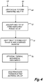
- FIG. 4 depicts a method of making thermoelectric material 12N and/or 12P containing dispersed phase 44 with coherent interfaces 46 according to the present invention.
- the method comprises mixing and heating a first material 64 and a second material 66 at step 68 to form melt 70.
- the chemical compositions of starting materials 64 and 66 are selected or intentionally formulated to create melt 70.
- Melt 70 is then solidified to form a single or multiple-phase solid in step 72. After solidification, the material is heated again at heat treating step 74 to allow the existing phases to further separate or precipitate into formations of dispersed phase 44 and to allow the host, or matrix, phase to homogenize.
- Dispersed phase 44 can form as any combination of spheroids, lamellar or rod-like structures, or as other shapes known to those in the art.
- the material can be optionally treated by standard thermal and/or mechanical means known in the art at step 76.
- thermoelectric material 12N and/or 12P is particularly important to maximize the thermoelectric performance of the material.
- host phase 42 it is preferable for host phase 42 to have commercially acceptable single-phase ZT values.
- semiconductors or semimetals are the best materials for this purpose because they have higher ZT than other classes of materials and are thus preferable materials for host phases 28 and 34.
- ZT is increased by adding or manipulating these structural features within host phases 28 and 34.
- materials with strong bonding affinity for host phase material 42 are considered as candidates for dispersed phase 44.
- materials having an element in common with host phase 42 are good candidates for dispersed phase 44.
- materials having an element in common with host phase 42 are good candidates for dispersed phase 44.
- materials having an element in common with host phase 42 are good candidates for dispersed phase 44.
- materials are selected that will phase separate from a melt to form host phase 42 and dispersed phase 44. Selection can be done by any number of methods, including examining binary phase diagrams to find materials where the elements of host phase 42 and dispersed phase 44 that are not common to each other do not alloy in the solid phase.
- lattice parameters of host phase 42 and dispersed phase 44 are compared and matched according to the limits discussed above to ensure adequate coherency of interface 46.
- phase systems are selected that exhibit a single phase field with a boundary with an adjacent multiple phase field whose solubility decreases with decreasing temperature leading to the potential of forming a supersaturated solid solution by quenching. Subsequent aging to precipitate one or more dispersed phases 44 can lead to materials with elevated ZT values.
- step 72 there are several methods of facilitating heating step 68 and solidification step 72.
- the particular solidification processes in step 72 are designed around initial materials 64 and 66 to selectively induce phase immiscibility between host phase 42 and dispersed phase 44.
- other embodiments of the invention include splat quenching, ribbon spinning, or inert gas powder atomization followed by post powder formation consolidation.
- Other embodiments include vacuum casting, mechanical alloying, mechanical mixing, directional solidification, injection mold processing, and reduction from an oxide.
- Heat treatment step 74 is also designed around the previous steps with a goal to achieve desired at least partial coherency and lattice match between phases 42 and 44 in one or more crystallographic directions. Other purposes of heat treatment step 74 include enhancing phase separation and matrix, or host phase, homogenization.
- Optional treatments step 76 are intended to further process the bulk-processed material, if necessary, to tailor or optimize thermoelectric and structural properties of the bulk-processed material.
- Two examples of such thermal and mechanical treatments include hot forging and elevated-temperature extrusion for overall particle alignment or texturing.
- Optional treatment step 76 can also be used to aid in further dispersion or isolation of any inclusion colonies 80 as shown below in FIG. 5A that may form in the bulk-processed material.
- dispersed phase 44 comprises materials with various degrees of thermal conductivity as well as various degrees of electrical conductivity, which further refines the thermoelectric properties of material 12N and/or 12P.
- One embodiment of the method depicted in FIG. 5 can be seen by way of example 1.
- a bismuth telluride - gallium telluride phase separated, bulk thermoelectric nanocomposite material with at least partially coherent interfaces is created.
- First material 64 is 4.662 g of bismuth telluride powder, 99.98% purity.
- Second material 66 is a combination of 0.09 g of gallium metal, 99.9999% purity in 6mm diameter pellets, and 0.248 g of tellurium powder, 99.99% purity, 325 mesh.
- the reagents are commercially available from laboratory supply companies such as Aldrich and Alfa Aesar.
- Bismuth telluride is an acceptable thermoelectric material and is used in several commercial applications, making it suitable for host phase 42.
- Gallium telluride has strong bonding affinity for bismuth telluride because of their common bridge element tellurium and the similar Te-Te spacings in each. This makes it suitable for dispersed phase 44. Further, according to the binary phase diagram, bismuth and gallium do not form an alloy at the temperatures used in the example.
- host phase 42 preferably has an acceptable ZT as a standalone material to maximize ZT in the bulk-processed material.
- host phase 42 can be a form of doped or undoped bismuth telluride. While the example discusses host phase 42 comprising undoped bismuth telluride, host phase 42 can alternatively be doped by materials including tin (Sn), antimony (Sb), lead (Pb), arsenic (As), selenium (Se), bromine (Br), and iodine (I), forming Bi 2-a X a Te 3 or Bi 2 X a Te 3-a .
- X is dopant selenium (Se) or antimony (Sb). The dopant may be selectively soluble in the host phase, and may be used to tailor p or n character.
- host phase 42 can also be self-doped by a nonstoichiometric amount of bismuth or tellurium, creating either bismuth-rich bismuth telluride compositions or bismuth-poor bismuth telluride compositions. If X is Bi or Te, the above formula then becomes Bi 2+ a Te 3 , where about -0.75 ⁇ a ⁇ 0.825. Doping the host phase is done for any number of purposes, one of which would be to increase ZT in the overall material. Another reason to dope host phase 42 would be in order to ensure that the bulk-processed material operates as an n-type or p-type material. As an example, selectively doping host phase 42 to make a material n-type or p-type would be beneficial in an apparatus similar to that depicted in FIG. 1 , where cooling apparatus 10 comprises alternating n-type and p-type materials.
- the composition of dispersed phase 44 also is selected to increase ZT according to the steps described above.
- the chemical composition of dispersed phase 44 affects not only the thermoelectric performance of the bulk-processed material in its own right, but the composition relative to host phase 42 also affects interface 46.
- the relative chemical compositions determine lattice match and chemical bonding affinity between phases 42 and 44, the impact of which is discussed above in reference to Figs. 3A and 3B .
- dispersed phase 44 is comprised of one or more of the following: a binary bismuth compound, a binary tellurium compound, a ternary bismuth compound, or a ternary tellurium compound.
- the dispersed phase comprises a binary tellurium compound (Y c Te d ), where Y is the second material in the binary tellurium compound, and both c and d reflect the stoichiometric balance of Y and Te in host phase 42.
- Y is aluminum (Al), chromium (Cr), cobalt (Co), copper (Cu), indium (In), iridium (Ir), iron (Fe), gallium (Ga), germanium (Ge), molybdenum (Mo), osmium (Os), rhenium (Re), ruthenium (Ru), silicon (Si), silver (Ag), tantalum (Ta), tungsten (W), vanadium (V) or zinc (Zn). More preferably, Y is gallium (Ga), indium (In), germanium (Ge), silver (Ag), copper (Cu), or zinc (Zn); and even more preferably Y is copper (Cu) or silver (Ag).
- Dispersed phase 44 can also be doped to fine-tune electron conductivity and phonon scattering performance. Doping dispersed phase 44 increases or decreases the number of charge carriers in the bulk-processed material and affects the relative Fermi energy levels of the overall system, thereby controlling thermoelectric performance of the bulk-processed material.
- dopant elements include copper (Cu), gold (Au), lead (Pb), cadmium (Cd), nickel (Ni), zinc (Zn), platinum (Pt), mercury (Hg), magnesium (Mg), silicon (Si), boron (B), gallium (Ga), carbon (C), germanium (Ge), indium (In), tin (Sn), antimony (Sb), arsenic (As), aluminum (Al), phosphorous (P) and silver (Ag).
- the dopants may be selectively soluble in the dispersed phase.
- Step 68 comprises mixing materials 64 and 66 in a nitrogen glovebox, placing them in a quartz ampoule, flame-sealing the ampoule under vacuum and placing it in a box furnace ramping to 800°C at 10°C per minute. After dwelling at 800°C for one hour, melt 70 is quenched in an ice water bath and solidified, step 72.
- Step 74 then comprises the solidified ingot being placed back in the box furnace and annealed at 390°C for 4 days to form desired aspect ratios and coherency between dispersed phase 44 and host phase 42 at interfaces 46. In this example, optional treatment 76 is skipped.
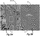
- FIG. 5A is a scanning electron micrograph of a sample area of a polished section of the bismuth telluride gallium telluride sample showing dispersoid free regions of bismuth telluride host phase 42 regions and a region containing a high density of submicron gallium telluride dispersoids.
- Bismuth telluride host phase 42 appears as light gray and gallium telluride dispersoids 44 are black in the micrograph.
- FIG. 5B is a higher magnification view of area 43 in FIG. 5A . The dispersoids appear as both spherical and rectangular shapes and the majority have submicron dimensions.
- FIG. 6 is a scanning electron micrograph indicating another example where dispersed phase 44 is predominantly spheroidal.
- dispersed phase 44 is copper telluride (Cu x Te y ) and matrix phase 42 is bismuth telluride selenide (Bi 2 Te 2.7 Se 0.3 ).
- Dispersed phase 44 is black and matrix phase 42 is gray in the micrograph.
- FIG. 7 shows an example wherein dispersed phase 44 comprises substantially lamellar or rod-like inclusions that appear to be crystallogrically related to the matrix phase.
- Matrix phase 42 is bismuth telluride selenide (Bi 2 Te 2.7 Se 0.3 ) and dispersed phase 44 is copper telluride (Cu x Te y ).
- Candidates for matrix phase 42 and dispersed phase 44 were considered according to the similarity of the tellurium atom spacings in both.
- the following table indicates two candidate systems with tellurium spacings of about 10 and 5 percent differences respectively.
- dispersed phase 44 causes a reduction in phonon thermal conductivity (k ph ) at least about 10 percent greater than an increase in electrical resistivity p, compared to k ph and p of the host phase alone is given here.
- the composite material product was measured to have a lattice thermal conductivity of 0.69 W/m-K.
- a second material product was produced the same exact way as the (BiTe 27 Se 3 ) 0.9 (Cu x Te y ) 0.1 composite phase but this time excluding the copper phase.
- This material product hereafter referred to as the "baseline material”
- This material was measured to have a lattice thermal conductivity of 1.14 W/m-K. The percent different between 0.69 W/m-K and 1.14 W/m-K is 39%.
- thermoelectric causes a reduction in rho-kappa (product of the material product's electrical resistivity, ⁇ , and its thermal conductivity, ⁇ ) at least about 10% compared to the rho-kappa of the host phase alone.
- the composite material product was measured to have a rho-kappa value of 20 ⁇ ohm-W/K.
- a second material product was produced the same exact way as the (BiTe 2.7 Se 3 ) 0.9 (Cu x Te y ) 0.1 composite phase but this time excluding the copper phase.
- This material product hereafter referred to as the "baseline material”
- This material was measured to have a rho-kappa value of 80 ⁇ ohm-W/K.
- the percent difference between 20 ⁇ ohm-W/K and 80 ⁇ ohm-W/K is 75%.
- FIG. 8 An example of at least partial dispersed phase 44 epitaxy with matrix phase 42 is shown in FIG. 8 .
- the figure shows an electron backscatter defraction (EBSD) image of gallium telluride (Ga 2 Te 3 ) dispersed phase 44 in bismuth telluride (Bi 2 Te) matrix phase 42.
- EBSD electron backscatter defraction
- the sample is a polished surface and regions 44 are gallium telluride (Ga 2 Te 3 ) dispersoids.
- Three bismuth telluride matrix grains are evident.
- Lower grain 90 is separated from middle bismuth telluride grain 92 by grain boundary 88.
- Middle bismuth telluride grain 92 is separated from upper bismuth telluride grain 94 by grain boundary 77.
- a predominant feature of EBSD inverse pole maps is that the specific crystalline orientation normal to the sample surface is indicated by specific shading in the image.
- the micrograph in FIG. 8 can be interpreted as indicating that many of the gallium telluride dispersoids in middle grain 92 have similar or identical orientations with respect to middle matrix grain 92 orientation.
- dispersoids 44 in upper grain 94 have identical shading indicating a similar or identical epitaxial relation with upper grain 94.
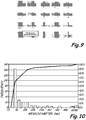
- FIG. 9 is a scanning electron micrograph of bismuth telluride selenide containing 10 atomic percent loading of copper telluride with the composition (BiTe 2.7 Se 3 ) 0.9 (Cu x Te y ) 0.1 .
- the copper telluride dispersoids appear as dark spots.
- An areal image analysis was made of the micrograph to determine the statistical distribution of the size of the dispersed phases. The results of the image analysis are plotted in FIG. 10 and are summarized in this following table.
- FIG. 11 is a scanning electron micrograph of bismuth telluride selenide containing 10 atomic percent loading of copper telluride with the composition (BiTe 2.7 Se 3 ) 0.9 (Cu x Te y ) 0.1 .
- the copper telluride dispersoids appear as dark spots.
- An areal image analysis was made of the micrograph to determine the statistical distribution of the size of the dispersed phases. The results of the image analysis are plotted in FIG. 12 and are summarized in this following table.
- semiconductor based bulk thermoelectric material systems have been identified that exhibit high ZT figures of merit.
- the materials consist of semiconducting host phases containing at least partially coherent submicron dispersed phases formed by at least a quench anneal process.
- the mechanism responsible for the ZT improvement is suggested to be phonon transport impedance due to the strain fields associated with each partially coherent submicron dispersoid phase.
- Inventive host phases include at least doped and undoped bismuth telluride and inventive dispersoid phases include at least binary or ternary bismuth or tellurium compounds.
Landscapes
- Chemical & Material Sciences (AREA)
- Engineering & Computer Science (AREA)
- Ceramic Engineering (AREA)
- Manufacturing & Machinery (AREA)
- Inorganic Chemistry (AREA)
- Materials Engineering (AREA)
- Structural Engineering (AREA)
- Organic Chemistry (AREA)
- Powder Metallurgy (AREA)
- Crystals, And After-Treatments Of Crystals (AREA)
- Silicon Compounds (AREA)
Description
- The present invention relates to the structure and performance of materials with useful thermoelectric characteristics at temperatures less than 200°C, and the production thereof by less expensive bulk material processing techniques.
- Thermoelectric materials exhibit a predictable relationship between their electrical and thermal performance. Depending on the desired outcome, a thermoelectric apparatus is frequently arranged as either a cooling/heat pump device or as an electrical power generator. To use the material as a cooling device or heat pump, an electric field is applied across the material, typically via an electric circuit. This field generates a thermal gradient according to the Peltier effect so long as it is maintained. Heat can be removed from the hot side of the material by a heat sink, heat exchanger or other heat removing means. When both are done simultaneously, the apparatus then operates effectively as a cooling device or heat pump. Conversely, creating a thermal gradient across the material, such as by application of thermal energy, induces an electric field according to the Seebeck effect. Connecting the material to a circuit aligned with this field causes the apparatus to operate effectively as an electrical power generator.
- There are numerous benefits of applying thermoelectric materials to cooling and electrical power generation. The total size of the thermoelectric materials and ancillary parts of a thermoelectric cooling apparatus can be relatively small compared to the size of an equivalent cooling system with typical components. Most typical cooling systems in current production utilize a vapor compression system, which requires at least a compressor, a working fluid, an expansion valve, an evaporator, and a condenser. Likewise, typical power generation facilities utilize large steam turbines to convert heat energy into electricity. A thermoelectric apparatus is smaller because there is less need to house this large, expensive equipment to convert energy from one form to another. This reduces the amount of space necessary to operate a cooling or power generation system, saving valuable functional space for a manufacturer, designer, or builder. Therefore, the compact size of thermoelectric materials the makes them ideal for many cooling and power generation applications where space is at a premium.
- End users also benefit from the virtual maintenance-free operation of a thermoelectric apparatus. Typical systems as described above use mechanical intermediaries to convert energy between a thermal form and an electrical form, while thermoelectric materials directly convert thermal energy to electrical energy without the need for mechanical intermediaries. Moving parts such as turbines, motors, and pumps, even if reliable, typically require periodic inspection and maintenance to minimize unplanned outages and major repairs and tend to reduce overall efficiencies. A thermoelectric apparatus has fewer such ancillary parts, and therefore fewer opportunities for system downtime.
- Despite the size and maintenance advantages over current systems, thermoelectric materials have to date been limited to certain niche and specialty applications. Key factors limiting widespread adoption of the technology are high production costs combined with the practical size requirements for thin film materials. The achievable thermoelectric performance of current materials, especially those designed to operate near room temperature, is also inadequate to make thermoelectric cooling systems competitive for many large scale operations, further restricting broad adoption of current thermoelectric technology.
- Current thermoelectric materials are best suited for applications with virtually no cost restrictions, that have a significant size constraint, or where reliability is more critical than efficiency. For example, current power generation applications include those in remote unattended land-based or space-based operations. Cooling technology using thermoelectric materials is generally limited to small-scale cooling applications, particularly in the medical and scientific fields. Thermoelectric cooling is penetrating the consumer market in certain specialty products such as portable refrigeration units and heated/cooled automotive seats. Each of these applications have particular reliability or size requirements that make thermoelectric cooling more attractive than standard vapor compression systems. In these applications, specialized needs outweigh the limited performance available from current thermoelectric materials.
- The performance of a thermoelectric material is characterized by its dimensionless figure-of-merit, ZT:

- As ZT increases, so does the conversion efficiency. While it is desirable to increase ZT by increasing S or decreasing ρ or k, there has been limited progress in the ability to beneficially change only one factor without causing a counteracting change in the other. For example, kel and p are related by the Wiedemann-Franz law, so that a decrease in p typically causes an offsetting increase in kel, resulting in no significant improvement. A reduction in kel can similarly cause an offsetting increase in p. These offsetting changes in kel and ρ typically result in no significant improvement in ZT. Most advances in thermoelectric performance have come from fabricating materials with reduced kph.
- However, selective reduction in kph has generally been possible only with labor and capital intensive thin film processes such as chemical vapor deposition. These processes reduce kph by creating successive phonon blocking layers or inclusions in one or two dimensions by building the materials several atoms at a time, but not in bulk. These current fabrication processes and their associated costs limit the size, performance, and application of thermoelectric materials.
- Not only do thin film products have a high production cost per unit volume, there are also practical size limits on materials produced via this process. Limits on thin film thermoelectric materials begin to arise in materials with thickness less than about 30 microns. At that level, parasitic losses begin to degrade overall device performance compared to the performance at the material level. Therefore, while vapor-deposited materials have relatively high ZT at room temperature, larger dimensioned thermoelectric materials are prohibitively expensive and insufficient for all but the most cost-insensitive applications.
US 2006/272697 discloses a process for producing bulk thermoelectric compositions containing nanoscale inclusions. The article by POUDEL ET AL.: "High-thermoelectric performance of nanostructured bismuth antimony telluride bulk alloys",SCIENCE, vol. 320, no. 5876, 2 May 2008 (2008-05-02), pages 634-638, XP008147704, discloses a nanostructured bismuth antimony telluride bulk alloy with a peak ZT of 1.4 at 100°C. - The present invention is a bulk-processed thermoelectric material, and a method for producing the same. According to a first aspect, the invention provides a bulk thermoelectric material comprising: a length, a width, and a thickness, wherein the length, width, and thickness are each at least about 30 µm; a host phase comprising bismuth telluride; a dispersed phase forming a plurality of inclusions comprised of one or more of: a binary bismuth compound, a binary tellurium compound, a ternary bismuth compound, or a ternary tellurium compound; an interface between the host phase and the dispersed phase that is substantially coherent in one crystallographic direction; and a thermoelectric figure of merit (ZT) greater than or equal to 1.0 at temperatures less than 200° C. The dispersed phase comprises a plurality of inclusions which form at least a partially coherent interface with matched interatomic distances of at least one shared atom with the host phase in at least one crystallographic direction.
- The method used to produce such a material includes selecting at least two starting materials that will form a host phase and a dispersed phase, then combining the materials by liquid phase or solid state precursor processing to form a dispersed phase in a matrix. The distribution, size, morphology, interfacial registry and electronic characteristics of the dispersed phase can be expediently and implicitly controlled by design of composition and processing (thermal, mechanical) parameters, without requiring the need for high-intensity and expensive thin film, nano-templating or atomic-manipulation fabrication/processing.
-
-
FIG. 1 is a schematic depiction of a thermoelectric cooling apparatus with bulk thermoelectric materials integrated into the apparatus. -
FIG. 2A is an exploded cross-sectional view of the structure of a bulk thermoelectric material having dispersed spheroidal inclusions of a second material within a host phase of a first material. -
FIG. 2B is an exploded cross-sectional view of the structure of a bulk thermoelectric material having dispersed lamellar or rod-like inclusions of a second material within a host phase of a first material. -
FIG. 3A is a diagram that depicts the microstructure of the bulk thermoelectric material near an inclusion and the effect of differing lattice structures on transport of phonons and charge carriers. -
FIG. 3B is a diagram that depicts the coherent phase interface by showing the crystallographic structure of an example material. -
FIG. 4 is a flow chart depicting a method of fabricating a bulk-processed thermoelectric material. -
FIG. 5A is a scanning electron micrograph of a bulk processed thermoelectric material comprising gallium telluride dispersoids in a bismuth telluride matrix. -
FIG. 5B is a higher magnification view ofarea 43 inFIG. 5A . -
FIG. 6 is a scanning electron micrograph of spheroidal copper telluride dispersoids in a bismuth telluride selenide matrix. -
FIG. 7 is a scanning electron micrograph of lamellar copper telluride dispersoids in a bismuth telluride selenide matrix. -
FIG. 8 is an electron backscatter diffraction (EBSD) image of gallium telluride dispersed phase in a bismuth telluride matrix. The image shown is an inverse pole map of the EBSD image. -
FIG. 9 is a scanning electron micrograph of copper telluride dispersoids in a bismuth telluride selenide matrix. -
FIG. 10 is a plot showing the size distribution of the copper telluride dispersoids inFIG. 9 . -
FIG. 11 is a scanning electron micrograph of copper telluride dispersoids in a bismuth telluride matrix. -
FIG. 12 is a plot showing the size distribution of the copper telluride dispersoids inFIG. 11 . -
FIG. 1 depicts a simplified schematic ofthermoelectric cooling apparatus 10 utilizing the Peltier effect to convert electrical energy into thermal gradient ΔT. Two bulk-processed thermoelectric materials,materials apparatus 10. Both have ZT values of at least about 1.0 at temperatures less than 100°C. In this illustration,materials - When input voltage V is applied to
electrical circuit 16, current flows as indicated byarrows 20. As current passes throughmaterials cold side 22 and towardhot side 24 as shown byarrow 18. Thermal gradient ΔT is maintained inmaterials arrows 20. When heat is simultaneously removed fromhot side 24 via heat rejection means such as a heat sink or heat exchanger (not shown), thermal gradient ΔT is maintained acrossmaterials cold side 22. - Thermal gradient ΔT is caused by the relative electrical and thermal energy carried by phonons and charge carriers through the microstructure of
materials materials FIGS. 2A and 2B , paths for each of these particles can be selectively changed to increase the thermoelectric effect. -
Materials FIGS. 2A and 2B . Spheroids and lamella are examples.FIG. 2A is an exploded cross-sectional view ofmicrostructure 40 of bulkthermoelectric material 12N and/or 12P comprising dispersedspheroidal inclusions 26 of a second material within ahost phase 28 comprising a first material. The contact areas betweeninclusions 26 andhost phase 28 define at least partially coherent interfaces 30.Charge carriers 52 can be holes or electrons depending on whether the thermoelectric material is n-type material 12N or p-type material 12P. Regardless of polarity,charge carriers 52 are believed to generally pass throughspheroidal inclusions 26 whilephonons 54 typically scatter atinterfaces 30 or within the strain fields associated with the interfaces. -
FIG. 2B is an exploded cross-sectional view of microstructure 41 of bulkthermoelectric material 12N and/or 12P comprising dispersed lamellar or rod-like inclusions 32 of a second material within ahost phase 34 of a first material. Similar toFIG. 2A , contact areas betweeninclusions 32 andhost phase 34 define interfaces 36. Also,charge carriers 52 are believed to generally pass throughinclusions 32 whilephonons 54 generally scatter atinterfaces 36 or within the strain fields associated with the interfaces. -
FIGS. 3A and3B illustrate the mechanism of this preferential scattering ofphonons 54 overcharge carriers 52FIG. 3A shows how dispersedphase 44 and resultingstrain field 48 operate to reduce the paths forphonons 54.FIG. 3B shows how paths remain available forcharge carriers 52 by makinginterface 46 at least partially coherent. - The differential scattering of
charge carriers 52 versusphonons 54 comes from the pathways available for each of them to travel throughmaterial 12N and/or 12P. To increase ZT, fewer pathways forphonons 54 must be available without reducing an offsetting number of pathways forcharge carriers 52.Charge carriers 52 travel throughchemical bonds 62, andphonons 54 are a manifestation of lattice vibrations that propagate via acoustic resonance. Preferably,thermoelectric material 12N and/or 12P should have substantially the same number ofbonds 62 that hostphase 42 has as a single material, while simultaneously creating lattice distortion to break up the resonance.FIG. 3A depicts how dispersedphase 44 preventsphonons 54 from propagating, and at least partiallycoherent interface 46 provides pathways forcharge carriers 52.FIG. 3B illustrates these pathways forcharge carriers 52 in more detail. -
FIG. 3A depicts a single inclusion and the surrounding structure within bulkthermoelectric material 12N and/or 12P.Microstructure 50 shows dispersedphase 44 at the center surrounded byhost phase 42. InFIG. 3A ,host phase 42 is schematically shown as a series of parallel and perpendicular crystal planes 43. Dispersedphase 44 is shown as a rectangular solid 45 with a smaller lattice parameter thanhost phase 42.Interface 46 forms at the outer surface of dispersedphase 44.Host phase 42 and dispersedphase 44 are depicted as crystal planes 43 and solid 45 for ease of illustration only and may be of any relative size and shape. Dispersedphase 44 can also have a lattice parameter larger thanhost phase 42. - In
FIG. 3A , the difference in the relative lattice parameters of dispersedphase 44 andhost phase 42 createsstrain field 48, depicted by dashed lines surrounding dispersedphase 44. Ascharge carriers 52 transport thermal energy towardhot side 24, the lattice begins to vibrate faster thancold side 22.Phonons 54 carry some of this thermal energy throughout the material as quantized vibration waves. Left alone, these vibrations cause a net transport of heat away fromhot side 24. However,strain field 48 effectively scattersphonons 54 passing throughbulk material 12N and/or 12P due to acoustic mismatch of the respective phases. Scattering atinterface 46 makes it more difficult for the thermal energy ofphonons 54 to migrate fromhot side 24 tocold side 22 inFIG. 1 , which is reflected in a reduced phonon contribution to thermal conductivity, kph . Reducing kph beneficially increases ZT by reducing the overall k value in the denominator of Equation 1 above. - Equation 1 also shows that reducing the charge carrier contribution, kel, would also beneficially increase ZT. It may appear from Equation 1 that kel could be reduced by reducing pathways for charge carriers. Unfortunately, the pathways used by
charge carriers 52 to carry thermal energy are the same pathways thatcharge carriers 52 use to carry electrical energy. Therefore, scattering charge carriers atinterface 46 to reduce kel would also result in an associated increase in electrical resistivity, ρ. - As a result, mobility of
charge carriers 52 betweenhost phase 42 and dispersedphase 44 must be substantially maintained inbulk material 12N and/or 12P by formingchemical bonds 62 atinterface 46 inFIG. 3B . Forming chemical bonds at a phase interface increases the coherency of the interface. Ifinterface 46 is not at least partially coherent, some or all of the beneficial increase in ZT resulting from the reduction of kph is offset by an increase of ρ from scattering ofcharge carriers 52 atinterface 46. -
FIG. 3B schematically illustrates the bond distortion in a single crystal due to a coherent inclusion with a larger lattice parameter in a matrix with a smaller lattice parameter. The coherent inclusion could also have a smaller lattice parameter in a matrix with a larger lattice parameter.FIG. 3B also illustrates the effect of this structure on mobility ofphonons 54 andcharge carriers 52. Instead of two separate lattices, makinginterface 46 at least partially coherent effectively creates a single distortedlattice 60. At the center of distortedlattice 60, the shaded area represents dispersedphase 44.Host phase 42 surrounds dispersedphase 44.Host phase 42 compriseshost phase atoms 56 and dispersedphase 44 comprises dispersedphase atoms 58 andhost phase atoms 56.Host phase 42 could have two or more different atom types and dispersedphase 44 could also have two or more different atom types where at least one of the atoms being the same element.Interface 46 is at least partially coherent when a plurality ofchemical bonds 62 form betweenhost phase atoms 56 and dispersedphase atoms 58. As shown inFIG. 3B , mobility ofcharge carriers 52 is supported by maintaining at least a portion of the original number ofbonds 62 through the material, particularly acrossinterface 46. - As discussed above, to increase ZT in material 12N and/or 12P compared to
host phase 42, the addition of dispersedphase 44 to hostphase 42 must cause a relative reduction in kph greater than the resulting increase in p. To achieve a satisfactory improvement in ZT, the relative reduction in kph caused by addition of dispersedphase 44 is preferably at least about 10% greater than the relative increase in ρ. More preferably the relative reduction in kph is at least about 50% greater than the relative increase in ρ, and even more preferably the relative reduction in kph is about 100% greater than the relative increase in p. - This preferential reduction in kph over an increase in ρ generally results in an overall reduction of the product of thermal conductivity and electrical resistivity pk. As described above, if ρk is reduced, the overall figure of merit ZT increases over that of
host phase 42. Here, the addition of dispersedphase 44 causes an overall reduction in pk, and a resulting increase in ZT of preferably at least about 10% overhost phase 42. The increase in ZT is more preferably at least about 50% greater and most preferably at least about 100% greater thanhost phase 42 without dispersedphase 44. - As shown in
FIG. 3B , reduction of kph by preferential phonon scattering is achieved by establishing at least partial coherency ofinterface 46. The potential for coherency depends on two key attributes ofhost phase 42 and dispersedphase 44. The presence of one or both attributes increases the likelihood of coherency and thus preferential scattering ofphonons 54. One attribute in determining coherency is the relative compatibility and alignment of atom spacings betweenhost phase 42 and dispersedphase 44. A second attribute, seen in several embodiments of the invention, is the sharing of at least one chemical element in common betweenhost phase 42 and dispersedphase 44. - The alignment of similar atom spacings ensures that the overall crystal structure of
host phase 42 is not significantly deformed by the presence of dispersedphase 44. As shown inFIG. 3A , substantial lattice deformation occurs atinterface 46 and induces astrong strain field 48.Strain field 48 is schematically depicted by dashed lines surrounding dispersedphase 44. As can be seen fromFIG. 3B ,bonds 62 will break atinterface 46 if the strain field is large enough, thereby reducing pathways forcharge carriers 52. Similar interatomic spacings of like atoms allow phases 42 and 44 to substantially align throughoutmaterial 12N and/or 12P, thereby maintainingchemical bonds 62 betweenphases charge carriers 52. This promotes lower electrical resistivity, ρ, and structural stability of the bulk-processed material atinterface 46 in at least one crystallographic direction. - This coherency of
interface 46 is optimized when the interatomic spacings of dispersedphase 44 are preferably within about ±10% of the interatomic spacings ofhost phase 42. The interatomic spacings of dispersedphase 44 are more preferably within about ±5% of the interatomic spacings ofhost phase 42, and even more preferably within about ±2% of the interatomic spacings ofhost phase 42. Those skilled in the art will recognize that any material of these dimensions produced by bulk-processing techniques will not be perfectly coherent and will have some imperfections, particularly in comparison to thin film techniques with nanometer-level control. However, the thermoelectric and cost performance will be improved over a thin film process for a large scale version of a given material. - In addition to lattice parameters, in several embodiments of this invention,
host phase atoms 56 and dispersedphase atoms 58 share at least one chemical element in common, which facilitates formation ofchemical bonds 62 betweenphases phases - Thermoelectric behavior is also determined in part by the selection of materials used in
host phase 42 and dispersedphase 44. The materials should be selected so as to have one element in common betweenhost phase 42 and dispersedphase 44. Whenhost phase atoms 56 and dispersedphase atoms 58 have at least one element in common, the shared elements ensure that there aresufficient bonds 62 to maximize the potential coherency ofinterface 46. - The relative concentrations of dispersed
phase 44 compared tohost phase 42 is yet another factor affecting the coherency ofinterface 46. As seen inFIG. 3B , the lattice distortion caused by dispersedphase 44 extends well intohost phase 42. When the concentration of dispersedphase 44 is increased, interfaces 46 and resulting distortions ofhost phase 42 necessarily move closer together. This reduction in space comes from a combination of larger inclusions, causing more lattice distortion inhost phase 42, or from a higher frequency of inclusions in a given volume. - Substantially all inclusions are preferably greater than about 1 nm and less than 1 µm across their smallest dimension. In one embodiment, substantially all inclusions range between 10 nm and 50 nm across their smallest dimension. In another embodiment, the material comprises a broad range of inclusions with about half ranging between about 10 nm to 50 nm across their smallest dimension with the substantial remainder of inclusions measuring between about 2 nm and 1 µm across their smallest dimension.
- In either case, this leaves less space for
host phase 42 to relax the lattice distortion and strain aroundinterface 46. When the distortion grows to a critical size,fewer bonds 62 will form atinterface 46, breaking down coherency and impeding transport ofcharge carriers 52. This lack of coherency resulting from high concentration of dispersedphase 44 thereby effectively increases ρ and kel directly and reduces ZT indirectly. - The opposite effect can also be seen in
FIG. 3B with a low concentration of dispersedphase 44. With relatively few lattice distortions separated by large distances, there is not enough surface area atinterfaces 46 to scatterphonons 54, leaving more of them free to pass fromhot side 24 tocold side 22 inFIG. 1 . Therefore, kph is not reduced sufficiently to materially increase ZT. The density and relative surface area of dispersedphase 44 also affects thermoelectric performance. To achieveinterfaces 46 with sufficient phonon scattering and electron conductivity, the ratio of the surface area to volume of substantially dispersedphase 44 is preferably greater than about 0.08 nm-1. In one embodiment, the ratio is greater than about 0.10 nm-1 and another embodiment, the ratio is between about 0.10 nm-1 and about 0.30 nm-1. - In terms of overall thermoelectric improvement based on relative phase concentrations, dispersed
phase 44 comprises less than about 40% by atomic composition of the bulk-processed material. In one embodiment, dispersedphase 44 is less than about 25% by atomic composition. In other embodiments, the phase concentration is less than about 15%, and in yet other embodiments, the phase concentration of dispersedphase 44 is between about 2% and about 12%. -
FIG. 4 depicts a method of makingthermoelectric material 12N and/or 12P containing dispersedphase 44 withcoherent interfaces 46 according to the present invention. The method comprises mixing and heating afirst material 64 and asecond material 66 atstep 68 to formmelt 70. The chemical compositions of startingmaterials melt 70.Melt 70 is then solidified to form a single or multiple-phase solid instep 72. After solidification, the material is heated again atheat treating step 74 to allow the existing phases to further separate or precipitate into formations of dispersedphase 44 and to allow the host, or matrix, phase to homogenize. Dispersedphase 44 can form as any combination of spheroids, lamellar or rod-like structures, or as other shapes known to those in the art. Afterheat treatment step 74, the material can be optionally treated by standard thermal and/or mechanical means known in the art atstep 76. - Selecting
initial materials thermoelectric material 12N and/or 12P is particularly important to maximize the thermoelectric performance of the material. First, it is preferable forhost phase 42 to have commercially acceptable single-phase ZT values. Typically, semiconductors or semimetals are the best materials for this purpose because they have higher ZT than other classes of materials and are thus preferable materials for host phases 28 and 34. InFIGS 2A and 2B , ZT is increased by adding or manipulating these structural features within host phases 28 and 34. - Second, materials with strong bonding affinity for
host phase material 42 are considered as candidates for dispersedphase 44. Preferably, materials having an element in common withhost phase 42 are good candidates for dispersedphase 44. Third, out of the potential candidates, materials are selected that will phase separate from a melt to formhost phase 42 and dispersedphase 44. Selection can be done by any number of methods, including examining binary phase diagrams to find materials where the elements ofhost phase 42 and dispersedphase 44 that are not common to each other do not alloy in the solid phase. Finally, of the remaining candidates for dispersedphase 44, lattice parameters ofhost phase 42 and dispersedphase 44 are compared and matched according to the limits discussed above to ensure adequate coherency ofinterface 46. - In another embodiment, phase systems are selected that exhibit a single phase field with a boundary with an adjacent multiple phase field whose solubility decreases with decreasing temperature leading to the potential of forming a supersaturated solid solution by quenching. Subsequent aging to precipitate one or more dispersed
phases 44 can lead to materials with elevated ZT values. - Once the materials are selected, there are several methods of facilitating
heating step 68 andsolidification step 72. The particular solidification processes instep 72 are designed aroundinitial materials host phase 42 and dispersedphase 44. In addition to the two step melt-quench process described in the example above, other embodiments of the invention include splat quenching, ribbon spinning, or inert gas powder atomization followed by post powder formation consolidation. Other embodiments include vacuum casting, mechanical alloying, mechanical mixing, directional solidification, injection mold processing, and reduction from an oxide. -
Heat treatment step 74 is also designed around the previous steps with a goal to achieve desired at least partial coherency and lattice match betweenphases heat treatment step 74 include enhancing phase separation and matrix, or host phase, homogenization. - Optional treatments step 76 are intended to further process the bulk-processed material, if necessary, to tailor or optimize thermoelectric and structural properties of the bulk-processed material. Two examples of such thermal and mechanical treatments include hot forging and elevated-temperature extrusion for overall particle alignment or texturing.
Optional treatment step 76 can also be used to aid in further dispersion or isolation of anyinclusion colonies 80 as shown below inFIG. 5A that may form in the bulk-processed material. In some embodiments of the invention, dispersedphase 44 comprises materials with various degrees of thermal conductivity as well as various degrees of electrical conductivity, which further refines the thermoelectric properties of material 12N and/or 12P. - One embodiment of the method depicted in
FIG. 5 can be seen by way of example 1. In this example, a bismuth telluride - gallium telluride phase separated, bulk thermoelectric nanocomposite material with at least partially coherent interfaces is created.First material 64 is 4.662 g of bismuth telluride powder, 99.98% purity.Second material 66 is a combination of 0.09 g of gallium metal, 99.9999% purity in 6mm diameter pellets, and 0.248 g of tellurium powder, 99.99% purity, 325 mesh. The reagents are commercially available from laboratory supply companies such as Aldrich and Alfa Aesar. - These
initial materials host phase 42. Gallium telluride has strong bonding affinity for bismuth telluride because of their common bridge element tellurium and the similar Te-Te spacings in each. This makes it suitable for dispersedphase 44. Further, according to the binary phase diagram, bismuth and gallium do not form an alloy at the temperatures used in the example. This ensures that bismuth telluride and gallium telluride will form out of a melt that includes bismuth, tellurium, and gallium, but also means that the melt is unlikely to form an unwanted bismuth-gallium phase or a ternary bismuth-gallium-tellurium phase. This satisfies the third factor of the selection method. Finally, the lattice parameters between host phase bismuth telluride and dispersed phase gallium telluride differ by less than 10%, thereby satisfying the final element of the selection method. - Further, the material comprising
host phase 42 preferably has an acceptable ZT as a standalone material to maximize ZT in the bulk-processed material. As described in the example,host phase 42 can be a form of doped or undoped bismuth telluride. While the example discusseshost phase 42 comprising undoped bismuth telluride,host phase 42 can alternatively be doped by materials including tin (Sn), antimony (Sb), lead (Pb), arsenic (As), selenium (Se), bromine (Br), and iodine (I), forming Bi2-aX a Te3 or Bi2XaTe3-a. Preferably, X is dopant selenium (Se) or antimony (Sb). The dopant may be selectively soluble in the host phase, and may be used to tailor p or n character. - In lieu of doping by a third element,
host phase 42 can also be self-doped by a nonstoichiometric amount of bismuth or tellurium, creating either bismuth-rich bismuth telluride compositions or bismuth-poor bismuth telluride compositions. If X is Bi or Te, the above formula then becomes Bi2+a Te3, where about -0.75 < a < 0.825. Doping the host phase is done for any number of purposes, one of which would be to increase ZT in the overall material. Another reason todope host phase 42 would be in order to ensure that the bulk-processed material operates as an n-type or p-type material. As an example, selectively dopinghost phase 42 to make a material n-type or p-type would be beneficial in an apparatus similar to that depicted inFIG. 1 , where coolingapparatus 10 comprises alternating n-type and p-type materials. - While the chemical composition of
host phase 42 provides the foundation for a high ZT bulk-processed material, the composition of dispersedphase 44 also is selected to increase ZT according to the steps described above. The chemical composition of dispersedphase 44 affects not only the thermoelectric performance of the bulk-processed material in its own right, but the composition relative to hostphase 42 also affectsinterface 46. The relative chemical compositions determine lattice match and chemical bonding affinity betweenphases Figs. 3A and3B . - To encourage coherency of
interface 46, whenhost phase 42 is bismuth telluride, dispersedphase 44 is comprised of one or more of the following: a binary bismuth compound, a binary tellurium compound, a ternary bismuth compound, or a ternary tellurium compound. Preferably, the dispersed phase comprises a binary tellurium compound (Y cTed ), where Y is the second material in the binary tellurium compound, and both c and d reflect the stoichiometric balance of Y and Te inhost phase 42. Preferably, Y is aluminum (Al), chromium (Cr), cobalt (Co), copper (Cu), indium (In), iridium (Ir), iron (Fe), gallium (Ga), germanium (Ge), molybdenum (Mo), osmium (Os), rhenium (Re), ruthenium (Ru), silicon (Si), silver (Ag), tantalum (Ta), tungsten (W), vanadium (V) or zinc (Zn). More preferably, Y is gallium (Ga), indium (In), germanium (Ge), silver (Ag), copper (Cu), or zinc (Zn); and even more preferably Y is copper (Cu) or silver (Ag). - The choice of elements listed above result in preferable dispersed
phase 44 compounds of aluminum telluride (Al2Te3), chromium telluride (Cr2Te3), cobalt telluride (CoTe), copper telluride (CuTe), dicopper telluride (Cu2Te), copper deficient dicopper telluride (Cu x Te, where 1.0 < x < 2.0), indium telluride (In2Te3), iridium telluride (IrTe2), iron telluride (FeTe), gallium telluride (Ga2Te3), germanium telluride (GeTe), molybdenum telluride (MoTe2), osmium telluride (OsTe2), rhenium telluride (ReTe2), ruthenium telluride (RuTe2), silicon telluride (SiTe2), silver telluride (Ag2Te), tantalum telluride (TaTe2), tungsten telluride (WTe2), vanadium telluride (VTe2) or zinc telluride (ZnTe). The more preferable dispersed phases would then comprise gallium telluride (Ga2Te3), germanium telluride (GeTe), silver telluride (Ag2Te), copper telluride (CuTe), dicopper telluride (Cu2Te), copper deficient dicopper telluride (Cu x Te, where 1.0 < x < 2.0), and zinc telluride (ZnTe). Even more preferable dispersed phases would comprise copper telluride (CuTe), dicopper telluride (Cu2Te), copper deficient dicopper telluride Cu x Te, where 1.0 < x < 2.0, and silver telluride (Ag2Te). - Dispersed
phase 44 can also be doped to fine-tune electron conductivity and phonon scattering performance. Doping dispersedphase 44 increases or decreases the number of charge carriers in the bulk-processed material and affects the relative Fermi energy levels of the overall system, thereby controlling thermoelectric performance of the bulk-processed material. Examples of dopant elements include copper (Cu), gold (Au), lead (Pb), cadmium (Cd), nickel (Ni), zinc (Zn), platinum (Pt), mercury (Hg), magnesium (Mg), silicon (Si), boron (B), gallium (Ga), carbon (C), germanium (Ge), indium (In), tin (Sn), antimony (Sb), arsenic (As), aluminum (Al), phosphorous (P) and silver (Ag). The dopants may be selectively soluble in the dispersed phase. - After selection of Bi2Te3 and Ga2Te3, the materials were then mixed and heated via
step 68 to formmelt 70.Step 68 comprises mixingmaterials step 72.Step 74 then comprises the solidified ingot being placed back in the box furnace and annealed at 390°C for 4 days to form desired aspect ratios and coherency between dispersedphase 44 andhost phase 42 at interfaces 46. In this example,optional treatment 76 is skipped. - The microstructure of the Bi2Te3-Ga2Te3 example discussed herein comprises areas of dispersoid free bismuth
telluride host phase 42 and areas ofhost phase 42 containing high densities of gallium telluride dispersoids.FIG. 5A is a scanning electron micrograph of a sample area of a polished section of the bismuth telluride gallium telluride sample showing dispersoid free regions of bismuthtelluride host phase 42 regions and a region containing a high density of submicron gallium telluride dispersoids. Bismuthtelluride host phase 42 appears as light gray and gallium telluride dispersoids 44 are black in the micrograph.FIG. 5B is a higher magnification view ofarea 43 inFIG. 5A . The dispersoids appear as both spherical and rectangular shapes and the majority have submicron dimensions. -
FIG. 6 is a scanning electron micrograph indicating another example where dispersedphase 44 is predominantly spheroidal. In the figure dispersedphase 44 is copper telluride (CuxTey) andmatrix phase 42 is bismuth telluride selenide (Bi2Te2.7 Se 0.3). Dispersedphase 44 is black andmatrix phase 42 is gray in the micrograph. -
FIG. 7 shows an example wherein dispersedphase 44 comprises substantially lamellar or rod-like inclusions that appear to be crystallogrically related to the matrix phase.Matrix phase 42 is bismuth telluride selenide (Bi2Te2.7 Se 0.3) and dispersedphase 44 is copper telluride (CuxTey). - Candidates for
matrix phase 42 and dispersedphase 44 were considered according to the similarity of the tellurium atom spacings in both. The following table indicates two candidate systems with tellurium spacings of about 10 and 5 percent differences respectively.Table: Comparison of Te atom spacings in candidate matrix and dispersoid materials. Matrix Te-Te Spacing Dispersoid Te-Te Spacing Δ Spacing Sb1.5Bi0.5Te3 4.297Ǻ Ag2Te 4.712Ǻ 9.7% Bi2Te3 4.395Ǻ Ga2Te3 4.169Ǻ 5.2% - An example where dispersed
phase 44 causes a reduction in phonon thermal conductivity (kph) at least about 10 percent greater than an increase in electrical resistivity p, compared to kph and p of the host phase alone is given here. A material product with the composition (BiTe2.7Se3)0.9(CuxTey)0.1, where BiTe2.7Se3 is the host phase at 90 atomic percent loading, and CuxTey is the dispersed phase at 10 atomic percent loading, was produced through a melt-quench-anneal route starting from the base elements as outline inFIG. 4 . The composite material product was measured to have a lattice thermal conductivity of 0.69 W/m-K. A second material product was produced the same exact way as the (BiTe27Se3)0.9(CuxTey)0.1 composite phase but this time excluding the copper phase. This material product, hereafter referred to as the "baseline material," has therefore a composition of BiTe2.7Se3. This material was measured to have a lattice thermal conductivity of 1.14 W/m-K. The percent different between 0.69 W/m-K and 1.14 W/m-K is 39%. - The following is an example demonstrating a material product wherein the presence of the dispersed phase in the bulk thermoelectric causes a reduction in rho-kappa (product of the material product's electrical resistivity, ρ, and its thermal conductivity, κ) at least about 10% compared to the rho-kappa of the host phase alone. A material product with the composition (BiTe2.7Se3)0.9(CuxTey)0.1, where BiTe2.7Se3 is the host phase at 90 atomic percent loading, and CuxTey is the dispersed phase at a 10 atomic percent loading, was produced through a melt-quench-anneal route starting from the base elements as outlined in
FIG. 4 . The composite material product was measured to have a rho-kappa value of 20 µohm-W/K. A second material product was produced the same exact way as the (BiTe2.7Se3)0.9(CuxTey)0.1 composite phase but this time excluding the copper phase. This material product, hereafter referred to as the "baseline material", has therefore a composition of BiTe2.7Se3. This material was measured to have a rho-kappa value of 80 µohm-W/K. The percent difference between 20 µohm-W/K and 80 µohm-W/K is 75%. - An example of at least partial dispersed
phase 44 epitaxy withmatrix phase 42 is shown inFIG. 8 . The figure shows an electron backscatter defraction (EBSD) image of gallium telluride (Ga2Te3) dispersedphase 44 in bismuth telluride (Bi2Te)matrix phase 42. The image shown is an inverse pole map of the EBSD image. The sample is a polished surface andregions 44 are gallium telluride (Ga2Te3) dispersoids. Three bismuth telluride matrix grains are evident.Lower grain 90 is separated from middlebismuth telluride grain 92 bygrain boundary 88. Middlebismuth telluride grain 92 is separated from upperbismuth telluride grain 94 bygrain boundary 77. - A predominant feature of EBSD inverse pole maps is that the specific crystalline orientation normal to the sample surface is indicated by specific shading in the image. As such, the micrograph in
FIG. 8 can be interpreted as indicating that many of the gallium telluride dispersoids inmiddle grain 92 have similar or identical orientations with respect tomiddle matrix grain 92 orientation. Similarly dispersoids 44 inupper grain 94 have identical shading indicating a similar or identical epitaxial relation withupper grain 94. -
FIG. 9 is a scanning electron micrograph of bismuth telluride selenide containing 10 atomic percent loading of copper telluride with the composition (BiTe2.7Se3)0.9 (CuxTey)0.1. The copper telluride dispersoids appear as dark spots. An areal image analysis was made of the micrograph to determine the statistical distribution of the size of the dispersed phases. The results of the image analysis are plotted inFIG. 10 and are summarized in this following table.Volume % Average Diameter Minimum Diameter Maximum Diameter 80th Percentile 50th Percentile 10.8 93.5 nm 21.8 nm 925.5 nm 123.5 nm 47.6 nm - In this sample, all dispersoids were submicron in size and half were sub 47.6 nm in size.
-
FIG. 11 is a scanning electron micrograph of bismuth telluride selenide containing 10 atomic percent loading of copper telluride with the composition (BiTe2.7Se3)0.9 (CuxTey)0.1. The copper telluride dispersoids appear as dark spots. An areal image analysis was made of the micrograph to determine the statistical distribution of the size of the dispersed phases. The results of the image analysis are plotted inFIG. 12 and are summarized in this following table.Volume % Average Diameter Minimum Diameter Maximum Diameter 80th Percentile 50th Percentile 10.1 38.3 nm 9.76 nm 1.42 µm 58.0 nm 18.2 nm - In this sample, all dispersoids were less than 1.42 µm in size and half were less than 18.2 nm in size.
- In summary, semiconductor based bulk thermoelectric material systems have been identified that exhibit high ZT figures of merit. The materials consist of semiconducting host phases containing at least partially coherent submicron dispersed phases formed by at least a quench anneal process. The mechanism responsible for the ZT improvement is suggested to be phonon transport impedance due to the strain fields associated with each partially coherent submicron dispersoid phase. Inventive host phases include at least doped and undoped bismuth telluride and inventive dispersoid phases include at least binary or ternary bismuth or tellurium compounds.
Claims (15)
- A bulk thermoelectric material comprising:a length, a width, and a thickness, wherein the length, width, and thickness are each at least about 30 µm;a host phase comprising bismuth telluride;a dispersed phase forming a plurality of inclusions comprised of one or more of:a binary bismuth compound, a binary tellurium compound, a ternary bismuth compound, or a ternary tellurium compound;an interface between the host phase and the dispersed phase that is substantially coherent in one crystallographic direction; anda thermoelectric figure of merit (ZT) greater than or equal to 1.0 at temperatures less than 200° C.
- The bulk thermoelectric material of claim 1, wherein the dispersed phase comprises substantially spheroidal inclusions or substantially lamellar or rod-like inclusions.
- The bulk thermoelectric material of claim 1, wherein each inclusion has a smallest dimension that measures between about 1 nanometers (nm) and about 1 micron (µm).
- The bulk thermoelectric material of claim 3, wherein at least half the inclusions measure between about 10 nm and about 50 nm across the smallest dimension.
- The bulk thermoelectric material of claim 1, wherein the host phase and the dispersed phase are crystalline with lattice parameters of the dispersed phase being within about ±10% of lattice parameters of the host phase.
- The bulk thermoelectric material of claim 1, wherein the dispersed phase has a surface area to volume ratio, defined by a sum of an outer surface area of the inclusions of the dispersed phase divided by the total volume of the bulk thermoelectric material, the surface area to volume ratio of the dispersed phase being at least about 0.08 nm-1.
- The bulk thermoelectric material of claim 1, wherein presence of the dispersed phase in the bulk thermoelectric material causes a reduction in phonon thermal conductivity (kph ) at least about 10% greater than an increase in electrical resistivity (ρ) compared to kph and p of the host phase alone.
- The bulk thermoelectric material of claim 1, wherein presence of the dispersed phase in the bulk thermoelectric material causes an increase of ZT of at least about 10% compared to the host phase alone.
- The bulk thermoelectric material of claim 1, wherein the host phase is doped, undoped, or self-doped bismuth telluride Bi2-aX a Te3 or Bi2XaTe3-a, where X is a doping material selected from one of bismuth (Bi), lead (Pb), arsenic (As), tin (Sn), bromine (Br), iodine (I), and antimony (Sb); and a is a relative stoichiometric quantity of X.
- The bulk thermoelectric material of claim 1 wherein the host phase is self doped bismuth telluride, Bi2+a Te3 wherein a is greater than or equal to about -0.75 and is less than about 0.825.
- The bulk thermoelectric material of claim 1, wherein the dispersed phase is doped with at least one of: copper (Cu), gold (Au), lead (Pb), cadmium (Cd), nickel (Ni), zinc (Zn), platinum (Pt), mercury (Hg), magnesium (Mg), silicon (Si), boron (B), gallium (Ga), carbon (C), germanium (Ge), indium (In), tin (Sn), antimony (Sb), arsenic (As), aluminum (Al), phosphorus (P), and silver (Ag).
- The bulk thermoelectric material of claim 1, wherein the dispersed phase comprises less than or equal to about 40% by atomic composition of the bulk-processed material.
- The bulk thermoelectric material of claim 1, exhibiting a phase boundary whose solubility between adjacent phase fields decreases with decreasing temperature.
- A method for making a thermoelectric material, the method comprising:heating a mixture of initial materials to form a melt, wherein the materials may consist of (i) simple elements, (ii) binary compounds or (iii) ternary alloys;solidifying the melt to induce phase separation, forming a bulk material comprising a host phase comprising bismuth telluride and a dispersed phase of inclusions comprised of one or more of: a binary bismuth compound, a binary tellurium compound, a ternary bismuth compound, or a ternary tellurium compound; andheat treating the bulk material to further precipitate the dispersed phase from the host phase and homogenize both phases wherein the dispersed phase is aligned with the host phase and coherent in at least one crystallographic direction, so that the bulk material has a thermoelectric figure of merit (ZT) of at least 1.0 at temperatures less than 200°C.
- The method of claim 14, wherein the mixture of materials are (i) simple elements, (ii) binary compounds or (iii) ternary alloys, wherein
the simple elements are selected from the group consisting of: bismuth (Bi), tellurium (Te) and/or antimony (Sb) and one or more of the following: thallium (Tl), selenium (Se), aluminum (Al), chromium (Cr), cobalt (Co), copper (Cu), iridium (Ir), iron (Fe), gallium (Ga), germanium (Ge), molybdenum (Mo), osmium (Os), rhodium (Rh), ruthenium (Ru), silicon (Si), silver (Ag), tantalum (Ta), tungsten (W), vanadium (V) or zinc (Zn),
the binary compounds are selected from the group consisting of bismuth telluride (Bi2Te3), bismuth selenide (Bi2Se3), and/or antimony telluride (Sb2Te3), and one or more of the following: thallium telluride (Tl2Te3), aluminum telluride (Al2Te3), chromium telluride (Cr2Te3), cobalt telluride (CoTe), copper telluride (Cu2Te), CuxTe where 1.0 ≤ x ≤ 2.0, iridium telluride (IrTe2), iron telluride (FeTe), gallium telluride (Ga2Te2), germanium telluride (GeTe), molybdenum telluride (MoTe2), osmium telluride (OsTe2), rhodium (RhTe2), ruthenium telluride (RuTe2), silicon telluride (SiTe2), silver telluride (Ag2Te), tantalum telluride (TaTe2), tungsten telluride (WTe2), vanadium telluride (VTe2) or zinc telluride (ZnTe), and
the ternary alloys are selected from the group consisting of Bi2Te1-xSex, Sb2-xBixTe3 or Sb2-xBixSe3.
Applications Claiming Priority (2)
| Application Number | Priority Date | Filing Date | Title |
|---|---|---|---|
| US13927008P | 2008-12-19 | 2008-12-19 | |
| PCT/US2009/066959 WO2010080279A2 (en) | 2008-12-19 | 2009-12-07 | Bulk-processed, enhanced figure-of-merit thermoelectric materials |
Publications (3)
| Publication Number | Publication Date |
|---|---|
| EP2359417A2 EP2359417A2 (en) | 2011-08-24 |
| EP2359417A4 EP2359417A4 (en) | 2014-03-19 |
| EP2359417B1 true EP2359417B1 (en) | 2017-08-23 |
Family
ID=42317048
Family Applications (1)
| Application Number | Title | Priority Date | Filing Date |
|---|---|---|---|
| EP09837821.9A Not-in-force EP2359417B1 (en) | 2008-12-19 | 2009-12-07 | Bulk-processed, enhanced figure-of-merit thermoelectric materials |
Country Status (4)
| Country | Link |
|---|---|
| US (1) | US8692106B2 (en) |
| EP (1) | EP2359417B1 (en) |
| CN (1) | CN102257648B (en) |
| WO (1) | WO2010080279A2 (en) |
Families Citing this family (35)
| Publication number | Priority date | Publication date | Assignee | Title |
|---|---|---|---|---|
| RU2011142629A (en) * | 2009-03-24 | 2013-04-27 | Басф Се | SELF-ORGANIZING THERMOELECTRIC MATERIALS |
| KR101663183B1 (en) * | 2010-08-26 | 2016-10-06 | 삼성전자주식회사 | Thermoelectric materials, and thermoelectric module and thermoelectric device comprising same |
| CN102403445B (en) * | 2010-09-07 | 2015-06-10 | 中国科学院福建物质结构研究所 | Bismuth telluride-based thermoelectric material and preparation method thereof |
| US8957299B2 (en) * | 2011-01-24 | 2015-02-17 | Samsung Electronics Co., Ltd. | Thermoelectric material including nano-inclusions, thermoelectric module and thermoelectric apparatus including the same |
| JP5853483B2 (en) * | 2011-08-12 | 2016-02-09 | トヨタ自動車株式会社 | Nanocomposite thermoelectric conversion material |
| TWI472069B (en) * | 2011-12-19 | 2015-02-01 | 財團法人工業技術研究院 | Thermoelectric composite |
| KR102001062B1 (en) | 2012-01-16 | 2019-10-01 | 삼성전자주식회사 | Thermoelectric nano-composite, and thermoelectric module and thermoelectric apparatus comprising same |
| DE102012000763A1 (en) * | 2012-01-18 | 2013-07-18 | Emitec Gesellschaft Für Emissionstechnologie Mbh | Semiconductor element and method for producing a tubular thermoelectric module |
| JP2013161989A (en) * | 2012-02-06 | 2013-08-19 | Yamagata Univ | Method for manufacturing crystal composition including bi2te3 crystal and 3d transition metal |
| KR101982279B1 (en) * | 2012-04-27 | 2019-08-28 | 삼성전자주식회사 | Thermoelectric material having high-density interface misfit dislocation, and thermoelectric device and module comprising the same |
| FR2991207B1 (en) * | 2012-06-04 | 2014-05-16 | Commissariat Energie Atomique | METHOD FOR MANUFACTURING THERMOELECTRIC MATERIAL |
| CN103579482B (en) * | 2012-07-25 | 2016-09-07 | 中国科学院上海硅酸盐研究所 | Bismuth telluride-based thermoelectric generating element and preparation method thereof |
| US9076712B2 (en) * | 2012-09-04 | 2015-07-07 | Massachusetts Institute Of Technology | Solid state cloaking for electrical charge carrier mobility control |
| TWI472070B (en) * | 2012-12-13 | 2015-02-01 | Ind Tech Res Inst | Thermoelectric composite material and manufacturing method thereof |
| CN103545442B (en) * | 2013-10-31 | 2016-03-02 | 华南师范大学 | Deformation-free block thermoelectric material during a kind of thermo-electric generation |
| JP6292664B2 (en) * | 2014-01-28 | 2018-03-14 | 株式会社豊島製作所 | Thermoelectric conversion material |
| CN105827149A (en) * | 2015-01-06 | 2016-08-03 | 厦门兰智科技有限公司 | Thermoelectric conversion device for absorbing and converting heat source energy multiple times |
| KR101997203B1 (en) * | 2015-07-21 | 2019-07-05 | 주식회사 엘지화학 | Compound semiconductor thermoelectric material and manufacturing method thereof |
| CN106435329A (en) * | 2016-09-30 | 2017-02-22 | 无锡市明盛强力风机有限公司 | Metal alloy heat conduction material and preparation method thereof |
| CN107445621B (en) * | 2017-09-06 | 2020-05-12 | 济南大学 | A Cu-Te nanocrystal/Cu2SnSe3 thermoelectric composite material and preparation method thereof |
| CN107706297B (en) * | 2017-10-16 | 2018-09-25 | 超晶科技(北京)有限公司 | A kind of thermoelectric conversion element and preparation method thereof based on β type telluride silicon materials |
| CN108447976B (en) * | 2018-02-05 | 2021-03-30 | 沈阳大学 | Method for regulating performance of n-type bismuth telluride film by crystal boundary |
| US10892396B2 (en) | 2018-06-19 | 2021-01-12 | The Regents Of The University Of Michigan | Stabilized copper selenide thermoelectric materials and methods of fabrication thereof |
| ES2697926A1 (en) * | 2018-10-04 | 2019-01-29 | Marquina Alexandra Noriega | PROCEDURE FOR THE OBTAINING OF A THERMOELECTRIC PAINT, HIGH PERFORMANCE PAINT OBTAINED WITH SUCH PROCEDURE AND USE OF THE SAME (Machine-translation by Google Translate, not legally binding) |
| KR102157779B1 (en) * | 2018-11-16 | 2020-09-18 | 한국세라믹기술원 | Bi2Te3 BASED COMPOSITE THERMOELECTRIC MATERIAL COMPRISING FeTe2 NANOPARTICLE AND MANUFACTURING THE SAME |
| US12279528B2 (en) | 2019-01-18 | 2025-04-15 | Lg Electronics Inc. | Thermoelectric material manufacturing method |
| DE112019006226T5 (en) * | 2019-01-18 | 2021-08-26 | Lg Electronics Inc. | THERMOELECTRIC MATERIAL AND METHOD FOR MANUFACTURING IT |
| CN111628071B (en) * | 2020-05-26 | 2022-01-25 | 电子科技大学 | Medium-temperature-range thermoelectric material and preparation method thereof |
| CN112802955B (en) * | 2021-01-15 | 2023-04-18 | 广西大学 | P-type Cu2Te-Ag2Te thermoelectric material and preparation method thereof |
| WO2022264664A1 (en) * | 2021-06-16 | 2022-12-22 | パナソニックIpマネジメント株式会社 | Thermoelectric conversion material, thermoelectric conversion element, thermoelectric conversion module, and method for producing thermoelectric conversion material |
| CN113307236B (en) * | 2021-06-21 | 2024-02-09 | 中国科学技术大学 | Single-layer or multi-layer CrTe3 film and preparation method thereof |
| CN116356172A (en) * | 2021-12-22 | 2023-06-30 | 中国石油天然气集团有限公司 | Ternary thermoelectric material and preparation method thereof |
| CN114408874B (en) * | 2022-01-12 | 2023-07-18 | 深圳热电新能源科技有限公司 | Bismuth telluride thermoelectric material based on entropy engineering and preparation method thereof |
| CN115196965B (en) * | 2022-07-25 | 2023-07-25 | 深圳先进电子材料国际创新研究院 | N-type bismuth telluride thermoelectric material and preparation method thereof |
| CN118004977B (en) * | 2024-02-01 | 2026-05-26 | 清华大学 | Bismuth telluride-based alloys and their processing methods |
Family Cites Families (8)
| Publication number | Priority date | Publication date | Assignee | Title |
|---|---|---|---|---|
| US5108515A (en) * | 1988-11-15 | 1992-04-28 | Director-General, Agency Of Industrial Science And Technology | Thermoelectric material and process for production thereof |
| JP3594008B2 (en) * | 2000-11-30 | 2004-11-24 | ヤマハ株式会社 | Thermoelectric material, manufacturing method thereof and Peltier module |
| KR100933967B1 (en) * | 2001-10-05 | 2009-12-28 | 넥스트림 써멀 솔루션즈, 인크. | Phonon blocking electron permeation compact structure |
| JP4286053B2 (en) * | 2003-05-08 | 2009-06-24 | 株式会社Ihi | THERMOELECTRIC SEMICONDUCTOR MATERIAL, THERMOELECTRIC SEMICONDUCTOR ELEMENT USING THE THERMOELECTRIC SEMICONDUCTOR MATERIAL, THERMOELECTRIC MODULE USING THE THERMOELECTRIC SEMICONDUCTOR ELEMENT, AND METHOD FOR PRODUCING THEM |
| JP2005072391A (en) * | 2003-08-26 | 2005-03-17 | Kyocera Corp | N-type thermoelectric material, manufacturing method thereof, and N-type thermoelectric element |
| US7465871B2 (en) * | 2004-10-29 | 2008-12-16 | Massachusetts Institute Of Technology | Nanocomposites with high thermoelectric figures of merit |
| US8865995B2 (en) | 2004-10-29 | 2014-10-21 | Trustees Of Boston College | Methods for high figure-of-merit in nanostructured thermoelectric materials |
| US7847179B2 (en) * | 2005-06-06 | 2010-12-07 | Board Of Trustees Of Michigan State University | Thermoelectric compositions and process |
-
2009
- 2009-12-07 EP EP09837821.9A patent/EP2359417B1/en not_active Not-in-force
- 2009-12-07 WO PCT/US2009/066959 patent/WO2010080279A2/en not_active Ceased
- 2009-12-07 US US13/139,744 patent/US8692106B2/en not_active Expired - Fee Related
- 2009-12-07 CN CN200980151017.4A patent/CN102257648B/en not_active Expired - Fee Related
Non-Patent Citations (1)
| Title |
|---|
| None * |
Also Published As
| Publication number | Publication date |
|---|---|
| US8692106B2 (en) | 2014-04-08 |
| CN102257648A (en) | 2011-11-23 |
| EP2359417A2 (en) | 2011-08-24 |
| WO2010080279A3 (en) | 2010-09-30 |
| US20110248210A1 (en) | 2011-10-13 |
| CN102257648B (en) | 2018-04-27 |
| EP2359417A4 (en) | 2014-03-19 |
| WO2010080279A2 (en) | 2010-07-15 |
Similar Documents
| Publication | Publication Date | Title |
|---|---|---|
| US8692106B2 (en) | Bulk-processed, enhanced figure-of-merit thermoelectric materials | |
| He et al. | High performance bulk thermoelectrics via a panoscopic approach | |
| Chen et al. | Recent progress of half-Heusler for moderate temperature thermoelectric applications | |
| Musah et al. | Isovalent substitution in metal chalcogenide materials for improving thermoelectric power generation–A critical review | |
| US6342668B1 (en) | Thermoelectric materials with filled skutterudite structure for thermoelectric devices | |
| US20110042607A1 (en) | Thermoelectric compositions and process | |
| Cho et al. | Superior thermoelectric cooling performance by suppressing bipolar diffusion effect and enhancing anisotropic texture in p-/n-type Bi2Te3 based compounds | |
| JP5024393B2 (en) | Nanocomposite thermoelectric conversion material and method for producing the same | |
| WO2011094635A2 (en) | Nanocomposites with high thermoelectric performance and methods | |
| Du et al. | Ru alloying induced enhanced thermoelectric performance in FeSi2-based compounds | |
| US6207888B1 (en) | Semiconductor materials with skutterudite type crystal lattice structures optimized for selected thermoelectric properties and methods of preparation | |
| Goldsmid | Review of thermoelectric materials | |
| US20100025616A1 (en) | MECHANICAL STRENGTH & THERMOELECTRIC PERFORMANCE IN METAL CHALCOGENIDE MQ (M=Ge,Sn,Pb and Q=S, Se, Te) BASED COMPOSITIONS | |
| Irfan et al. | Revolutionizing energy harvesting: A comprehensive review of thermoelectric devices | |
| US11482654B2 (en) | Stabilized copper selenide thermoelectric materials and methods of fabrication thereof | |
| KR20210109639A (en) | Method of manufacturing thermoelectric material | |
| Fan et al. | Thermoelectric properties of p-type Te-doped (Bi, Sb) 2Te3 alloys by mechanical alloying and plasma activated sintering | |
| Xu et al. | Glass-like thermal conductivity in higher manganese silicides with grain boundary nanostructures | |
| HK1164544A (en) | Bulk-processed, enhanced figure-of-merit thermoelectric materials | |
| HK1164544B (en) | Bulk-processed, enhanced figure-of-merit thermoelectric materials | |
| Goldsmid | Review of thermoelectric materials | |
| Krez | Thermoelectric properties in phase-separated half-Heusler materials | |
| Singh et al. | Nanostructuring effects on thermoelectric properties | |
| Akter | Engineered Thermoelectric Materials for Energy Harvesting | |
| Bhatt et al. | Strategic control of excess tellurium to achieve high figure-of-merit in Te-rich Bi |
Legal Events
| Date | Code | Title | Description |
|---|---|---|---|
| PUAI | Public reference made under article 153(3) epc to a published international application that has entered the european phase |
Free format text: ORIGINAL CODE: 0009012 |
|
| 17P | Request for examination filed |
Effective date: 20110516 |
|
| AK | Designated contracting states |
Kind code of ref document: A2 Designated state(s): AT BE BG CH CY CZ DE DK EE ES FI FR GB GR HR HU IE IS IT LI LT LU LV MC MK MT NL NO PL PT RO SE SI SK SM TR |
|
| DAX | Request for extension of the european patent (deleted) | ||
| REG | Reference to a national code |
Ref country code: DE Ref legal event code: R079 Ref document number: 602009047977 Country of ref document: DE Free format text: PREVIOUS MAIN CLASS: H01L0035280000 Ipc: H01L0035160000 |
|
| A4 | Supplementary search report drawn up and despatched |
Effective date: 20140217 |
|
| RIC1 | Information provided on ipc code assigned before grant |
Ipc: H01L 35/16 20060101AFI20140211BHEP Ipc: C04B 35/653 20060101ALI20140211BHEP Ipc: C04B 35/457 20060101ALI20140211BHEP Ipc: H01L 35/26 20060101ALI20140211BHEP |
|
| 17Q | First examination report despatched |
Effective date: 20160303 |
|
| GRAP | Despatch of communication of intention to grant a patent |
Free format text: ORIGINAL CODE: EPIDOSNIGR1 |
|
| STAA | Information on the status of an ep patent application or granted ep patent |
Free format text: STATUS: GRANT OF PATENT IS INTENDED |
|
| INTG | Intention to grant announced |
Effective date: 20170307 |
|
| GRAS | Grant fee paid |
Free format text: ORIGINAL CODE: EPIDOSNIGR3 |
|
| GRAA | (expected) grant |
Free format text: ORIGINAL CODE: 0009210 |
|
| STAA | Information on the status of an ep patent application or granted ep patent |
Free format text: STATUS: THE PATENT HAS BEEN GRANTED |
|
| AK | Designated contracting states |
Kind code of ref document: B1 Designated state(s): AT BE BG CH CY CZ DE DK EE ES FI FR GB GR HR HU IE IS IT LI LT LU LV MC MK MT NL NO PL PT RO SE SI SK SM TR |
|
| REG | Reference to a national code |
Ref country code: GB Ref legal event code: FG4D |
|
| REG | Reference to a national code |
Ref country code: CH Ref legal event code: EP |
|
| REG | Reference to a national code |
Ref country code: AT Ref legal event code: REF Ref document number: 922207 Country of ref document: AT Kind code of ref document: T Effective date: 20170915 |
|
| REG | Reference to a national code |
Ref country code: IE Ref legal event code: FG4D |
|
| REG | Reference to a national code |
Ref country code: DE Ref legal event code: R096 Ref document number: 602009047977 Country of ref document: DE |
|
| REG | Reference to a national code |
Ref country code: FR Ref legal event code: PLFP Year of fee payment: 9 |
|
| REG | Reference to a national code |
Ref country code: NL Ref legal event code: FP |
|
| REG | Reference to a national code |
Ref country code: LT Ref legal event code: MG4D |
|
| REG | Reference to a national code |
Ref country code: AT Ref legal event code: MK05 Ref document number: 922207 Country of ref document: AT Kind code of ref document: T Effective date: 20170823 |
|
| PG25 | Lapsed in a contracting state [announced via postgrant information from national office to epo] |
Ref country code: FI Free format text: LAPSE BECAUSE OF FAILURE TO SUBMIT A TRANSLATION OF THE DESCRIPTION OR TO PAY THE FEE WITHIN THE PRESCRIBED TIME-LIMIT Effective date: 20170823 Ref country code: NO Free format text: LAPSE BECAUSE OF FAILURE TO SUBMIT A TRANSLATION OF THE DESCRIPTION OR TO PAY THE FEE WITHIN THE PRESCRIBED TIME-LIMIT Effective date: 20171123 Ref country code: AT Free format text: LAPSE BECAUSE OF FAILURE TO SUBMIT A TRANSLATION OF THE DESCRIPTION OR TO PAY THE FEE WITHIN THE PRESCRIBED TIME-LIMIT Effective date: 20170823 Ref country code: LT Free format text: LAPSE BECAUSE OF FAILURE TO SUBMIT A TRANSLATION OF THE DESCRIPTION OR TO PAY THE FEE WITHIN THE PRESCRIBED TIME-LIMIT Effective date: 20170823 Ref country code: HR Free format text: LAPSE BECAUSE OF FAILURE TO SUBMIT A TRANSLATION OF THE DESCRIPTION OR TO PAY THE FEE WITHIN THE PRESCRIBED TIME-LIMIT Effective date: 20170823 Ref country code: SE Free format text: LAPSE BECAUSE OF FAILURE TO SUBMIT A TRANSLATION OF THE DESCRIPTION OR TO PAY THE FEE WITHIN THE PRESCRIBED TIME-LIMIT Effective date: 20170823 |
|
| PG25 | Lapsed in a contracting state [announced via postgrant information from national office to epo] |
Ref country code: PL Free format text: LAPSE BECAUSE OF FAILURE TO SUBMIT A TRANSLATION OF THE DESCRIPTION OR TO PAY THE FEE WITHIN THE PRESCRIBED TIME-LIMIT Effective date: 20170823 Ref country code: IS Free format text: LAPSE BECAUSE OF FAILURE TO SUBMIT A TRANSLATION OF THE DESCRIPTION OR TO PAY THE FEE WITHIN THE PRESCRIBED TIME-LIMIT Effective date: 20171223 Ref country code: LV Free format text: LAPSE BECAUSE OF FAILURE TO SUBMIT A TRANSLATION OF THE DESCRIPTION OR TO PAY THE FEE WITHIN THE PRESCRIBED TIME-LIMIT Effective date: 20170823 Ref country code: GR Free format text: LAPSE BECAUSE OF FAILURE TO SUBMIT A TRANSLATION OF THE DESCRIPTION OR TO PAY THE FEE WITHIN THE PRESCRIBED TIME-LIMIT Effective date: 20171124 Ref country code: ES Free format text: LAPSE BECAUSE OF FAILURE TO SUBMIT A TRANSLATION OF THE DESCRIPTION OR TO PAY THE FEE WITHIN THE PRESCRIBED TIME-LIMIT Effective date: 20170823 Ref country code: BG Free format text: LAPSE BECAUSE OF FAILURE TO SUBMIT A TRANSLATION OF THE DESCRIPTION OR TO PAY THE FEE WITHIN THE PRESCRIBED TIME-LIMIT Effective date: 20171123 |
|
| PG25 | Lapsed in a contracting state [announced via postgrant information from national office to epo] |
Ref country code: RO Free format text: LAPSE BECAUSE OF FAILURE TO SUBMIT A TRANSLATION OF THE DESCRIPTION OR TO PAY THE FEE WITHIN THE PRESCRIBED TIME-LIMIT Effective date: 20170823 Ref country code: DK Free format text: LAPSE BECAUSE OF FAILURE TO SUBMIT A TRANSLATION OF THE DESCRIPTION OR TO PAY THE FEE WITHIN THE PRESCRIBED TIME-LIMIT Effective date: 20170823 Ref country code: CZ Free format text: LAPSE BECAUSE OF FAILURE TO SUBMIT A TRANSLATION OF THE DESCRIPTION OR TO PAY THE FEE WITHIN THE PRESCRIBED TIME-LIMIT Effective date: 20170823 |
|
| REG | Reference to a national code |
Ref country code: DE Ref legal event code: R097 Ref document number: 602009047977 Country of ref document: DE |
|
| PG25 | Lapsed in a contracting state [announced via postgrant information from national office to epo] |
Ref country code: SK Free format text: LAPSE BECAUSE OF FAILURE TO SUBMIT A TRANSLATION OF THE DESCRIPTION OR TO PAY THE FEE WITHIN THE PRESCRIBED TIME-LIMIT Effective date: 20170823 Ref country code: IT Free format text: LAPSE BECAUSE OF FAILURE TO SUBMIT A TRANSLATION OF THE DESCRIPTION OR TO PAY THE FEE WITHIN THE PRESCRIBED TIME-LIMIT Effective date: 20170823 Ref country code: EE Free format text: LAPSE BECAUSE OF FAILURE TO SUBMIT A TRANSLATION OF THE DESCRIPTION OR TO PAY THE FEE WITHIN THE PRESCRIBED TIME-LIMIT Effective date: 20170823 Ref country code: SM Free format text: LAPSE BECAUSE OF FAILURE TO SUBMIT A TRANSLATION OF THE DESCRIPTION OR TO PAY THE FEE WITHIN THE PRESCRIBED TIME-LIMIT Effective date: 20170823 |
|
| PLBE | No opposition filed within time limit |
Free format text: ORIGINAL CODE: 0009261 |
|
| STAA | Information on the status of an ep patent application or granted ep patent |
Free format text: STATUS: NO OPPOSITION FILED WITHIN TIME LIMIT |
|
| REG | Reference to a national code |
Ref country code: CH Ref legal event code: PL |
|
| 26N | No opposition filed |
Effective date: 20180524 |
|
| PG25 | Lapsed in a contracting state [announced via postgrant information from national office to epo] |
Ref country code: SI Free format text: LAPSE BECAUSE OF FAILURE TO SUBMIT A TRANSLATION OF THE DESCRIPTION OR TO PAY THE FEE WITHIN THE PRESCRIBED TIME-LIMIT Effective date: 20170823 |
|
| REG | Reference to a national code |
Ref country code: IE Ref legal event code: MM4A |
|
| PG25 | Lapsed in a contracting state [announced via postgrant information from national office to epo] |
Ref country code: LU Free format text: LAPSE BECAUSE OF NON-PAYMENT OF DUE FEES Effective date: 20171207 Ref country code: MT Free format text: LAPSE BECAUSE OF NON-PAYMENT OF DUE FEES Effective date: 20171207 |
|
| REG | Reference to a national code |
Ref country code: BE Ref legal event code: MM Effective date: 20171231 |
|
| PG25 | Lapsed in a contracting state [announced via postgrant information from national office to epo] |
Ref country code: IE Free format text: LAPSE BECAUSE OF NON-PAYMENT OF DUE FEES Effective date: 20171207 |
|
| PG25 | Lapsed in a contracting state [announced via postgrant information from national office to epo] |
Ref country code: CH Free format text: LAPSE BECAUSE OF NON-PAYMENT OF DUE FEES Effective date: 20171231 Ref country code: LI Free format text: LAPSE BECAUSE OF NON-PAYMENT OF DUE FEES Effective date: 20171231 Ref country code: BE Free format text: LAPSE BECAUSE OF NON-PAYMENT OF DUE FEES Effective date: 20171231 |
|
| PG25 | Lapsed in a contracting state [announced via postgrant information from national office to epo] |
Ref country code: HU Free format text: LAPSE BECAUSE OF FAILURE TO SUBMIT A TRANSLATION OF THE DESCRIPTION OR TO PAY THE FEE WITHIN THE PRESCRIBED TIME-LIMIT; INVALID AB INITIO Effective date: 20091207 Ref country code: MC Free format text: LAPSE BECAUSE OF FAILURE TO SUBMIT A TRANSLATION OF THE DESCRIPTION OR TO PAY THE FEE WITHIN THE PRESCRIBED TIME-LIMIT Effective date: 20170823 |
|
| PG25 | Lapsed in a contracting state [announced via postgrant information from national office to epo] |
Ref country code: CY Free format text: LAPSE BECAUSE OF NON-PAYMENT OF DUE FEES Effective date: 20170823 |
|
| PG25 | Lapsed in a contracting state [announced via postgrant information from national office to epo] |
Ref country code: MK Free format text: LAPSE BECAUSE OF FAILURE TO SUBMIT A TRANSLATION OF THE DESCRIPTION OR TO PAY THE FEE WITHIN THE PRESCRIBED TIME-LIMIT Effective date: 20170823 |
|
| PG25 | Lapsed in a contracting state [announced via postgrant information from national office to epo] |
Ref country code: TR Free format text: LAPSE BECAUSE OF FAILURE TO SUBMIT A TRANSLATION OF THE DESCRIPTION OR TO PAY THE FEE WITHIN THE PRESCRIBED TIME-LIMIT Effective date: 20170823 |
|
| PG25 | Lapsed in a contracting state [announced via postgrant information from national office to epo] |
Ref country code: PT Free format text: LAPSE BECAUSE OF FAILURE TO SUBMIT A TRANSLATION OF THE DESCRIPTION OR TO PAY THE FEE WITHIN THE PRESCRIBED TIME-LIMIT Effective date: 20170823 |
|
| REG | Reference to a national code |
Ref country code: DE Ref legal event code: R079 Ref document number: 602009047977 Country of ref document: DE Free format text: PREVIOUS MAIN CLASS: H01L0035160000 Ipc: H10N0010852000 |
|
| PGFP | Annual fee paid to national office [announced via postgrant information from national office to epo] |
Ref country code: NL Payment date: 20221123 Year of fee payment: 14 Ref country code: GB Payment date: 20221116 Year of fee payment: 14 Ref country code: FR Payment date: 20221122 Year of fee payment: 14 Ref country code: DE Payment date: 20221122 Year of fee payment: 14 |
|
| REG | Reference to a national code |
Ref country code: DE Ref legal event code: R119 Ref document number: 602009047977 Country of ref document: DE |
|
| REG | Reference to a national code |
Ref country code: NL Ref legal event code: MM Effective date: 20240101 |
|
| GBPC | Gb: european patent ceased through non-payment of renewal fee |
Effective date: 20231207 |
|
| PG25 | Lapsed in a contracting state [announced via postgrant information from national office to epo] |
Ref country code: NL Free format text: LAPSE BECAUSE OF NON-PAYMENT OF DUE FEES Effective date: 20240101 |
|
| PG25 | Lapsed in a contracting state [announced via postgrant information from national office to epo] |
Ref country code: NL Free format text: LAPSE BECAUSE OF NON-PAYMENT OF DUE FEES Effective date: 20240101 |
|
| PG25 | Lapsed in a contracting state [announced via postgrant information from national office to epo] |
Ref country code: DE Free format text: LAPSE BECAUSE OF NON-PAYMENT OF DUE FEES Effective date: 20240702 |
|
| PG25 | Lapsed in a contracting state [announced via postgrant information from national office to epo] |
Ref country code: GB Free format text: LAPSE BECAUSE OF NON-PAYMENT OF DUE FEES Effective date: 20231207 |
|
| PG25 | Lapsed in a contracting state [announced via postgrant information from national office to epo] |
Ref country code: FR Free format text: LAPSE BECAUSE OF NON-PAYMENT OF DUE FEES Effective date: 20231231 |
|
| PG25 | Lapsed in a contracting state [announced via postgrant information from national office to epo] |
Ref country code: GB Free format text: LAPSE BECAUSE OF NON-PAYMENT OF DUE FEES Effective date: 20231207 Ref country code: FR Free format text: LAPSE BECAUSE OF NON-PAYMENT OF DUE FEES Effective date: 20231231 Ref country code: DE Free format text: LAPSE BECAUSE OF NON-PAYMENT OF DUE FEES Effective date: 20240702 |