EP2351220B1 - Parasitic capacitance cancellation in capacitive measurement applications - Google Patents
Parasitic capacitance cancellation in capacitive measurement applications Download PDFInfo
- Publication number
- EP2351220B1 EP2351220B1 EP09764432.2A EP09764432A EP2351220B1 EP 2351220 B1 EP2351220 B1 EP 2351220B1 EP 09764432 A EP09764432 A EP 09764432A EP 2351220 B1 EP2351220 B1 EP 2351220B1
- Authority
- EP
- European Patent Office
- Prior art keywords
- charge
- circuit
- sense plate
- plate structure
- capacitive
- Prior art date
- Legal status (The legal status is an assumption and is not a legal conclusion. Google has not performed a legal analysis and makes no representation as to the accuracy of the status listed.)
- Active
Links
- 238000005259 measurement Methods 0.000 title claims description 76
- 230000003071 parasitic effect Effects 0.000 title description 38
- 239000003990 capacitor Substances 0.000 claims description 195
- 238000012546 transfer Methods 0.000 claims description 84
- 238000000034 method Methods 0.000 claims description 36
- 230000008859 change Effects 0.000 claims description 15
- 230000035945 sensitivity Effects 0.000 claims description 12
- 238000001514 detection method Methods 0.000 claims description 10
- 238000000691 measurement method Methods 0.000 claims description 9
- 238000012261 overproduction Methods 0.000 claims description 2
- 230000000694 effects Effects 0.000 description 19
- 230000001965 increasing effect Effects 0.000 description 6
- 230000008901 benefit Effects 0.000 description 5
- 230000008569 process Effects 0.000 description 5
- XUIMIQQOPSSXEZ-UHFFFAOYSA-N Silicon Chemical compound [Si] XUIMIQQOPSSXEZ-UHFFFAOYSA-N 0.000 description 4
- 238000004519 manufacturing process Methods 0.000 description 4
- 238000004458 analytical method Methods 0.000 description 3
- 238000013461 design Methods 0.000 description 3
- 238000010586 diagram Methods 0.000 description 3
- 230000007774 longterm Effects 0.000 description 3
- 229910052710 silicon Inorganic materials 0.000 description 3
- 239000010703 silicon Substances 0.000 description 3
- 238000013459 approach Methods 0.000 description 2
- 239000013256 coordination polymer Substances 0.000 description 2
- 230000008878 coupling Effects 0.000 description 2
- 238000010168 coupling process Methods 0.000 description 2
- 238000005859 coupling reaction Methods 0.000 description 2
- 238000007599 discharging Methods 0.000 description 2
- 230000007613 environmental effect Effects 0.000 description 2
- 230000006870 function Effects 0.000 description 2
- 230000003993 interaction Effects 0.000 description 2
- 238000012360 testing method Methods 0.000 description 2
- 241001125929 Trisopterus luscus Species 0.000 description 1
- 235000002017 Zea mays subsp mays Nutrition 0.000 description 1
- 241000482268 Zea mays subsp. mays Species 0.000 description 1
- 230000003044 adaptive effect Effects 0.000 description 1
- 230000003321 amplification Effects 0.000 description 1
- 230000009286 beneficial effect Effects 0.000 description 1
- 230000003247 decreasing effect Effects 0.000 description 1
- 238000005516 engineering process Methods 0.000 description 1
- 238000001914 filtration Methods 0.000 description 1
- 230000036039 immunity Effects 0.000 description 1
- 230000006872 improvement Effects 0.000 description 1
- 230000001939 inductive effect Effects 0.000 description 1
- 230000010354 integration Effects 0.000 description 1
- 238000012544 monitoring process Methods 0.000 description 1
- 238000003199 nucleic acid amplification method Methods 0.000 description 1
- 238000012545 processing Methods 0.000 description 1
- 230000035484 reaction time Effects 0.000 description 1
- 230000000630 rising effect Effects 0.000 description 1
Images


Classifications
-
- H—ELECTRICITY
- H03—ELECTRONIC CIRCUITRY
- H03K—PULSE TECHNIQUE
- H03K17/00—Electronic switching or gating, i.e. not by contact-making and –breaking
- H03K17/94—Electronic switching or gating, i.e. not by contact-making and –breaking characterised by the way in which the control signals are generated
- H03K17/945—Proximity switches
- H03K17/955—Proximity switches using a capacitive detector
-
- G—PHYSICS
- G01—MEASURING; TESTING
- G01D—MEASURING NOT SPECIALLY ADAPTED FOR A SPECIFIC VARIABLE; ARRANGEMENTS FOR MEASURING TWO OR MORE VARIABLES NOT COVERED IN A SINGLE OTHER SUBCLASS; TARIFF METERING APPARATUS; MEASURING OR TESTING NOT OTHERWISE PROVIDED FOR
- G01D5/00—Mechanical means for transferring the output of a sensing member; Means for converting the output of a sensing member to another variable where the form or nature of the sensing member does not constrain the means for converting; Transducers not specially adapted for a specific variable
- G01D5/12—Mechanical means for transferring the output of a sensing member; Means for converting the output of a sensing member to another variable where the form or nature of the sensing member does not constrain the means for converting; Transducers not specially adapted for a specific variable using electric or magnetic means
- G01D5/14—Mechanical means for transferring the output of a sensing member; Means for converting the output of a sensing member to another variable where the form or nature of the sensing member does not constrain the means for converting; Transducers not specially adapted for a specific variable using electric or magnetic means influencing the magnitude of a current or voltage
- G01D5/24—Mechanical means for transferring the output of a sensing member; Means for converting the output of a sensing member to another variable where the form or nature of the sensing member does not constrain the means for converting; Transducers not specially adapted for a specific variable using electric or magnetic means influencing the magnitude of a current or voltage by varying capacitance
- G01D5/241—Mechanical means for transferring the output of a sensing member; Means for converting the output of a sensing member to another variable where the form or nature of the sensing member does not constrain the means for converting; Transducers not specially adapted for a specific variable using electric or magnetic means influencing the magnitude of a current or voltage by varying capacitance by relative movement of capacitor electrodes
- G01D5/2417—Mechanical means for transferring the output of a sensing member; Means for converting the output of a sensing member to another variable where the form or nature of the sensing member does not constrain the means for converting; Transducers not specially adapted for a specific variable using electric or magnetic means influencing the magnitude of a current or voltage by varying capacitance by relative movement of capacitor electrodes by varying separation
-
- G—PHYSICS
- G01—MEASURING; TESTING
- G01R—MEASURING ELECTRIC VARIABLES; MEASURING MAGNETIC VARIABLES
- G01R27/00—Arrangements for measuring resistance, reactance, impedance, or electric characteristics derived therefrom
- G01R27/02—Measuring real or complex resistance, reactance, impedance, or other two-pole characteristics derived therefrom, e.g. time constant
- G01R27/26—Measuring inductance or capacitance; Measuring quality factor, e.g. by using the resonance method; Measuring loss factor; Measuring dielectric constants ; Measuring impedance or related variables
- G01R27/2605—Measuring capacitance
-
- G—PHYSICS
- G01—MEASURING; TESTING
- G01R—MEASURING ELECTRIC VARIABLES; MEASURING MAGNETIC VARIABLES
- G01R27/00—Arrangements for measuring resistance, reactance, impedance, or electric characteristics derived therefrom
- G01R27/02—Measuring real or complex resistance, reactance, impedance, or other two-pole characteristics derived therefrom, e.g. time constant
- G01R27/26—Measuring inductance or capacitance; Measuring quality factor, e.g. by using the resonance method; Measuring loss factor; Measuring dielectric constants ; Measuring impedance or related variables
- G01R27/2611—Measuring inductance
-
- H—ELECTRICITY
- H03—ELECTRONIC CIRCUITRY
- H03K—PULSE TECHNIQUE
- H03K2217/00—Indexing scheme related to electronic switching or gating, i.e. not by contact-making or -breaking covered by H03K17/00
- H03K2217/94—Indexing scheme related to electronic switching or gating, i.e. not by contact-making or -breaking covered by H03K17/00 characterised by the way in which the control signal is generated
- H03K2217/96—Touch switches
- H03K2217/9607—Capacitive touch switches
- H03K2217/96071—Capacitive touch switches characterised by the detection principle
- H03K2217/960725—Charge-transfer
Definitions
- This invention relates to the compensation of parasitic or unwanted capacitance in capacitance measurement applications.
- CN101150309 discloses an adaptive capacitive touch sensitive control circuit.
- EP1406069 discloses a fingerprint identification system that makes use of a capacitance sensor.
- US 2008/061800 discloses methods, systems and devices for detecting a measurable capacitance using sigma-delta charge transfer techniques.
- the invention also relates to an embodiment of the charge transfer method that overcomes the effect of non-linearity in a charging capacitor and enables scaling of a capacitor so that the method can be implemented practically and economically on standard CMOS integrated circuits.
- an integrated circuit comprising a capacitive measurement circuit for use in a capacitive measurement apparatus, as defined in independent Claim 1.
- a method of adjusting the number of charge transfer cycles in a capacitive measurement cycle of a capacitive charge transfer measurement circuit which includes a sense plate structure, as defined in independent Claim 13. The capacitance measurement may be done by repeatedly transferring charge from a capacitor to be measured (C M ) to a reference capacitor (C R ).
- the reference capacitor (C R ) starts in a known initial state (e.g. 0V).
- the measured capacitor C M is charged to a known state (e.g. Vdd).
- Charge is transferred from C M to C R .
- One such cycle is defined as a "Charge Transfer Cycle”. As more Charge Transfer Cycles are performed the charge, and thus the voltage, on C R increases.
- the Charge Transfer Cycles continue until C R reaches a specific voltage level (trip level).
- the time to charge the reference capacitor from the initial state to the trip level is defined as the "measurement period".
- the number of transfers in the measurement period is an indication of the size of C M .
- each Charge Transfer Cycle an additional unwanted amount of charge is transferred from C M to C R because of parasitic capacitances (C P ) in the circuit.
- This invention relates to the removal of this additional unwanted charge originating from the parasitic capacitances (C P ), from C R , during each Charge Transfer Cycle so that only the charge from C M remains on C R after a Charge Transfer Cycle. This compensates for the effect of the parasitic capacitances (C P ) and only the wanted, measured capacitance on C M is measured.
- the sensitivity of the process can be increased by reducing the effective value of C M . This means that not only can the parasitic capacitances be removed, but that C M can be adjusted to have a specific capacitance. This must be done without a physical change to the sensor structure (sense plate/antenna). One way to implement this is described hereinafter.
- the above capacitance measurement method is still applicable if the reference capacitor (C R ) and measured capacitor (C M ) are interchanged.
- Another charge transfer measurement technique is to perform a set number of Charge Transfer Cycles and measure the final voltage on the reference capacitor C R . This method is described in detail in US7148704 by Phillip and in other literature. The same method of compensation for parasitic capacitances (C P ) as described above can also be applied for other charge transfer and general capacitive measurement techniques.
- the effect of parasitic capacitance (C P ) is cancelled by removing the same amount of charge that the C P added to C R in each Charge Transfer Cycle.
- C P parasitic capacitance
- the amount of charge the C P and C M capacitors add to C R in each Charge Transfer Cycle is not the same from one Charge Transfer Cycle to the next.
- This removal of charge is accomplished by pre-charging a compensation capacitor (C C ) and then connecting this C C to the C R capacitor.
- parasitic capacitance cancellation is handled by means of a current mirror structure.
- a capacitor C PC that defines the parasitic capacitance to be cancelled is charged or discharged after being charged to the same value as C M (e.g. Vdd).
- C M e.g. Vdd
- the current flowing is then mirrored and extracted from C R .
- This C PC is not necessarily the real parasitic capacitance in the circuit, it is merely a user or designer defined parameter. This has two significant advantages.
- the current mirror structure is well suited for scaling the current.
- the reference current (I R ) flowing from C PC can be mirrored (I R : I S ).
- the notation 1:1 means the exact same current will flow in the secondary circuit; 1:0.5 (or 2:1) gives 50% of the current in the secondary; and 1:2 results in the current in the secondary circuit being doubled.
- This enables the designer to scale the capacitors, such as C PC , in order to optimise for performance, cost, signal to noise ratio or other design parameters.
- the C PC is charged to a fixed level or discharged from a fixed level to create the reference current. Because of the current mirror operation and characteristics the secondary circuit current (I S ) flowing from C R is independent of the voltage level of C R . This means the charge added to C R due to the parasitic capacitance can be removed in a way that is constant in every charge/discharge cycle i.e. essentially in the same way that it is added. This provides for a linear operation in removing charge from the C R . This, coupled with the implementation described below for handling the charge transfers from C M in the same manner, allows a more linear system is achieved.
- C M is discharged through the current mirror to a fixed voltage (e.g. ground).
- a reference current I R
- I S related current
- This current can be made to flow into C R transferring the related charge. Due to the characteristics of the current mirror element the current is independent of the voltage level on C R and as such results in the linear charging of C R because the amount of charge transferred is related to the charge flowing from C M and not to the voltage level of C R .
- the current mirror or other mirror element can have a ratio between the I R and I S currents. For example if the ratio is a step down ratio of a 1000 then it is possible to reduce the value of C R a 1000 times and still get the same number of transfers. This means a C R that may not be practical to embed in a normal CMOS IC (e.g. 20nF) can be reduced to a value that can very reasonably be implemented on-chip (e.g. 20pF). This results in significant savings in cost through reducing discrete components (cost and manufacturing) as well as reducing pin count, or coupling of noise.
- the ratio is a step down ratio of a 1000 then it is possible to reduce the value of C R a 1000 times and still get the same number of transfers.
- the scaling of charge is used in a charge transfer measurement circuit to facilitate integration of capacitive elements into a standard CMOS integrated circuit.
- a parasitic capacitance cancellation circuit in which scaling of charge is effected through a current mirror structure to scale capacitive elements that define or determine the charge which is to be removed from C R during each charge transfer cycle.
- the current mirror structure may result in a removal of charge from a reference capacitor in a way that is independent of the voltage level of the reference capacitor.
- the invention also extends to a parasitic capacitance cancellation method in which unwanted additional charge which is transferred by a parasitic capacitor to a reference capacitor is removed by a separate compensation capacitor.
- parasitic capacitance cancellation is used in a general sense and extends to the cancellation of capacitance inherent to the antenna, sense plate or sensor electrode structure.
- the unwanted additional charge from the parasitic capacitor is removed during each Charge Transfer Cycle.
- the unwanted additional charge from the parasitic capacitor produced in one Charge Transfer Cycle is removed during a following Charge Transfer Cycle.
- a capacitance cancellation circuit is implemented using the current mirror structure and any applicable ratio for extracting current from C R .
- a reference current is used that flows for a defined period of time.
- the capacitance measurement approach can also benefit from an algorithm designed to obtain certain performance objectives.
- the goal may be sensitivity in which case it would be beneficial to remove as much capacitance as is practical through the capacitance cancellation method or circuit.
- the choice of a larger reference capacitor is better and as such forces a lower capacitance cancellation value.
- the algorithm needs to take into account the interplay between at least the following group of parameters or subsets thereof: the counts per measurement, the reference capacitor size, the amount of capacitance cancellation, current mirror ratios, the noise in the environment, the transfer frequency, etc.
- the noise specifically "looks" like or can manifest itself in signals as a genuine signal related for example to a proximity event, it does interfere with operation of the measurement circuit. As such, it is desirable to be able to detect the presence of RTS noise and then to remove the effect of the RTS noise.
- RTS noise it is possible to look for sudden variations or jumps in measurements, but this may coincide with, or may be similar in form to, normal operational events from sense plate signals.
- the same parts of the measurement circuit e.g. current mirror and capacitance cancellation circuit
- This internal measurement can then be used to indicate the presence or absence of such noise.
- this indication of presence of RTS noise may be used to inhibit proximity detections/indications at the time, but still allow touch indications because the RTS noise is not big enough to cause such false measurements.
- the change in measurement caused by the RTS noise is quantified and then removed from the measurement signals to yield a "clean" signal on which detection decisions are based.
- This may be done through analysis of the change in value of the measurement on the internal system, with no external sense plate and only internal components (e.g. fixed capacitors inside the IC for C M and C R ), or by monitoring the external signal and measuring changes that occur at the time of RTS noise detection or when the noise falls away.
- a quantum of the noise influence on the signal can be determined and the effect thereof removed. In one example such quantum may be added or removed from the long term average to effectively negate its effect in the measurement system.
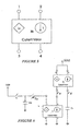
- Figure 1 shows a charge transfer circuit as well as a parasitic capacitance cancellation circuit.
- a reference capacitor (C R ) is initialized to a known voltage Va (e.g. 0V) by closing a switch S1.
- the Charge Transfer Cycle consists of at least 4 phases, viz the Charge Phase (UP), the Transfer Phase (PASS) and two Deadtime Phases ( Figure 2 ) which ensure that the Charge Phase and the Transfer Phase do not overlap.
- UP Charge Phase
- PASS Transfer Phase
- Figure 2 Two Deadtime Phases
- S3, S5 and S7 are closed and switches S2, S4 and S6 are open.
- a measured capacitor (C M ) as well as the parasitic capacitance (C P ) are charged to a reference voltage (Vdd).
- Capacitors C M and Cp are connected to the reference capacitor (C R ) and charge is transferred from C M and C P to C R .
- the voltage on C R at the end of the Transfer Phase is V CR .
- the parasitic capacitance (C P ) adds Cp(Vdd - V CR ) charge to C R . This is the amount of charge that the parasitic capacitance cancellation circuit must remove during each Charge Transfer Cycle.
- a compensation capacitor C C is pre-charged to (Vdd-V CR ) and thus C C has a charge of C C (Vdd-V CR ). This charge is supplied by the buffer and the supply voltage (Vdd). No charge is added to or removed from C R .
- Figure 5 shows graphically the mirror structure required.
- the circuit is connected so that a reference current (I R ) flows between nodes 1 and 3.
- the mirror element is shown in a general circuit for charge transfer measurement.
- C M the capacitor the value of which must be measured
- S 1 Charge Phase
- S 2 Transfer Phase
- the resulting current (I R ) flows through the current mirror element between nodes 1 and 3.
- This same current is connected to a second mirror ratio structure and this results in a current n(kI R ) flowing between nodes 6 and 8.
- the initial reference current I R is multiplied first by a factor k and then by a factor n. In a specific situation k and n are each smaller than 1.
- This current forces charge into C R , charging it with a charge that is related through the factor nk with the charge flowing from C M to ground.
- This technique results in a linear charging of C R i.e. the voltage level on C R rises in equal steps for each Charge Transfer Cycle and does not fall away as results from charging C M directly into C R . After each Charge Transfer Cycle the voltage level on C R can be checked to see if a trip level has been reached.
- the current mirror can be a single current mirror or use can be made of two or more current mirrors. This does not affect the implementation of the invention.
- the two stage implementation is merely an example that works well in practice.
- Figure 7 shows the parasitic capacitance cancellation structure.
- the value of parasitic capacitance to be cancelled can be selectively varied through the various switches available. If the three capacitors shown are used more charge will be removed from C R every cycle.
- the switching selection of the capacitors can be done under software control to automatically calibrate products for optimum operation.
- a product can be designed and the PCC (parasitic capacitance cancellation) can be used to tune automatically for, say, 4000 transfers, when no touch is present. In this way manufacturing variations can be compensated for.
- the adjustment of a trip level can also be used in an equivalent way to adjusting the C R value. Moving the trip level higher is equivalent to enlarging the C R and vice versa.
- Figures 8A and 8B show how the charge to be removed during capacitance cancellation can be determined by choosing between various reference current sources ( Figure 8B ) rather than capacitors ( Figure 8A ).
- a capacitor charged to a specific voltage contains a defined charge. This charge, divided or multiplied via current mirror ratios, is used to define the charge that is removed in the capacitance cancellation technique.
- the same effect ( Figure 8B ) can be achieved using current as a reference for the charge, instead of capacitance.
- a defined current flowing for a specific period of time also defines a charge.
- the charge can be taken out of C R using a current during the complete cycle or during a portion of each cycle. All that is required is that the period (i.e. main oscillator) and amplitude of current remain stable. As mentioned before this may be attractive in terms of implementation on silicon.
- the charge may also be determined by another technique applicable to the specific situation without affecting the other teachings and advantages of this invention.
- CMOS complementary metal-oxide-semiconductor
- CMOS complementary metal-oxide-semiconductor
- the use of currents to remove charge from the C R can also have advantages for the capacitive cancellation implementation in the sense that switching every Charge Transfer Cycle is not needed for the cancellation circuit.
- the cancellation current can flow continuously and as long as the charge transfer frequency is stable a fixed ratio between charge added from the C M to C R and the charge removed from C R will be maintained. If C M changes, the ratio will also change to reflect the changed capacitance measured.
- Figure 9 shows a circuit diagram based on an integrated circuit from Azoteq (Pty) Ltd based on a charge transfer measurement method using current mirror ratios and capacitive cancellation techniques. It is apparent that only a few external components are required and that all C R 's have been implemented on-chip.
- the implementation of current ratio structures makes the on-chip implementation of components practical and at the same time makes possible the selection and implementation on-chip of at least one such component, multiple components or combinations of such components.
- the integrated circuit (U2) (IQS127 from Azoteq (Pty) Ltd) comprises all the building blocks for the capacitive measurement circuit including the current mirror for scaling the charge transferred from the sense plate (which is connected to pad SNS_PLT) to U2 and the capacitive cancellation circuit that contains several capacitors to select from to predetermine the capacitance that is removed.
- An external resistor R 1 is used to increase protection against electrostatic discharge (ESD) from the sense plate to U2.
- Capacitors C 1 and C 2 are for voltage regulation and help to assure a good, stable and noise free supply voltage to the IC U2.
- the device (U2) provides two outputs namely an indication of proximity detection on POUT, and a touch (i.e. much stronger capacitance variation detected) on TOUT.
- Figures 10A and 10B are two flow charts of respective algorithms for automatic adjustment of parameters to achieve certain performance objectives.
- the algorithm in Figure 10A uses the largest acceptable size of C R as a metric to aim for and requires less capacitive cancellation to achieve a certain charge transfer count per cycle.
- the algorithm in Figure 10B aims to have the largest acceptable capacitive cancellation amount and this results in a smaller C R value.
- the Figure 10B algorithm also results in more sensitive settings for capacitive measurements.
- the current mirror ratios can also be used to interplay with the C R values or the capacitive cancellation. Explanation of ATI terms ATI Antenna Tuning Implementation.
- C R Reference Capacitor (Four size selections) CC Bits Capacitance Cancellation size selection (0 to 256) Current Sample The number of charge transfers for the current sense channel ATI Target The preselected number of charge transfers that the ATI algorithm aims for CRI_DIV
- CRI_DIV Select flag Flag to indicate the C R current mirror divider ratio must be selected
- Select flag Flag to indicate the C R size must be selected
- ATI_INIT flag Flag to indicate the initial difference (with all the PCC bits set to zero) between the current sample and the ATI target must be stored ATI_AT_MIN flag Flag to indicate the current sample cannot be adjusted lower ATI AT_MAX flag Flag to indicate the current sample cannot be adjusted higher Long Term Average
- a filtered value of the current sample Reseed Flag Flag to indicate the long term average must be loaded with the current sample value
- the aim of the ATI algorithm is to adjust the relevant parameters (C R size, C R current mirror ratio and the PCC bits) to get the current sample as close as possible to the ATI target count value. This will ensure that the circuit adjusts itself to obtain repeatable performance despite manufacturing and other tolerances.
- the ATI algorithm can be implemented in a number of ways. Two possible algorithms are presented.
- the first algorithm in Figure 10A Stability Enhancement
- CC capacitive cancellation
- the second algorithm in Figure 10B Sensitivity Enhancement
- the ATI_BUSY flag is set to indicate to the system that ATI is in progress.
- the CC bits are set to zero, the current mirror divider ratio is set to a higher value and the C R size is set to a maximum value.
- the CRI-DIV Select flag is also set to force the system to do a determination if the higher value is the optimal selection.
- the system then completes a charge transfer cycle [104]. If it is determined that the CRI_DIV Select flag is set [106] a test is done to check whether the current sample is bigger than the ATI target [138]. If it is bigger the current mirror divider ratio is changed to the lower value [136], the CRI_DIV Select flag is cleared and the CR Select flag is set [134] to force the selection of the appropriate C R size.
- the CR Select flag is set [108].
- the current sample is checked against the ATI target [142]. If the current sample is smaller than the ATI target the CR Select flag is cleared and the ATI_INIT flag is set [140] to start the process of determining the appropriate CC value to get the current sample the closest to the ATI target.
- the C R size is reduced [144] to the next smaller value until the current sample is smaller than the ATI target. If the minimum value of C R size is reached [146] the ATI_AT_MIN flag is set [148] to indicate the current sample cannot be adjusted any lower than its current value.
- the ATI_INIT flag is set [110].
- the current CC value (zero) is stored together with the difference between the current sample and the target [134].
- the ATI_INIT flag is also cleared.
- the algorithm will then keep increasing the CC value [120] and storing the smallest difference value and the CC value that yielded the smallest difference value [118] until either the current sample is at double the target value [112] or the maximum value for the CC is reached [122]. On either of these conditions the CC value that yielded the smallest difference in relation to the target is loaded and a reseed is forced [130].
- the ATI_BUSY flag is set to indicate to the system that ATI is in progress.
- the CC bits are set to a third of the maximum value. This will result in the algorithm selecting a smaller C R value with a higher CC value resulting in higher sensitivity.
- the current mirror divider ratio is set to the lower value and the C R size is set to the maximum value.
- the CRI_DIV Select flag is also set to force the system to do a determination if the lower value is the optimal selection.
- the system then completes a charge transfer cycle [204]. If it is determined that the CRI_DIV Select flag is set [206] a test is done to check whether the current sample is smaller than the ATI target [238]. If it is smaller, the current mirror divider ratio is changed to the higher value [236], the CRI_DIV Select flag is cleared and the CR Select flag is set [234] to force the selection of the appropriate C R size.
- the CR Select flag will be set [208].
- the current sample is checked against the ATI target [242]. If the current sample is smaller than the ATI target the CR Select flag is cleared and the ATI_INIT flag is set [240] to start the process of determining the appropriate CC value to get the current sample the closest to the ATI target.
- the CC value is also set to zero.
- the C R size is reduced [244] to the next smaller value until the current sample is smaller than the ATI target. If the minimum value of C R size is reached the ATI_AT_MIN flag is set [248] to indicate the current sample cannot be adjusted any lower than its current value.
- the ATI_INIT flag is set [210].
- the current CC value (zero) is stored together with the difference between the current sample and the target [234].
- the ATI_INIT flag is also cleared.
- the algorithm will then keep increasing the CC value [220] and storing the smallest difference value and the CC value that yielded the smallest difference value [218] until either the current sample is at double the target value [212] or the maximum value for the CC is reached [222]. On either of these conditions the CC value that yielded the smallest difference in relation to the target is loaded and a reseed is forced [230]
- FIG 11 illustrates an example of a circuit-noise detection structure which is specifically aimed at noise generated on-chip.
- An example of the type of noise is Random Conduct Signal noise (RTS noise) which results in substantial steps in the measurements and which is it not typically Gaussian by nature.
- the normal implementation incorporates the sense plate, C RX (a reference capacitor for external measurement) and C CX (a reference capacitor for capacitance cancellation of the external sense plate), connected through switches S 1 , S 3 and S 5 respectively to a measurement circuit (IC) 320.
- S 1 is the "PASS" switch in a charge transfer implementation.
- the "UP" switch is not shown.
- C MI internal measurement capacitor
- C Cl defines the amount of charge to be removed for the internal measurement. It is important to incorporate as many elements of the circuit as possible for the internal measurement, within the IC.
- the detection of RTS noise in accordance with the preceding description triggers an analysis of the normal measurement data and an automatic learning algorithm is then implemented to model the noise manifestation from these measurements. It is then possible to remove the effects of this noise automatically from the measurement signal when the noise occurs or when it disappears.
- the size (amplitude) of the internal noise is used to derive an effect (through scaling etc) of the noise on the normal measurement and the effect of the noise can be removed.
- Figure 12 shows an implementation for capacitive cancellation to reduce or remove the effect of noise amplification when the charge removal is done after the current mirror.
- a switch S 1 is a PASS switch that transfers the charge from the Sense Plate (C M ) to the current mirror (M1) that mirrors the charge which is transferred as per the ratio (1:X) into the C R where the charge is accumulated to be measured in some way. For example, a fixed trip level may be set and the number of transfers may be counted, or a fixed number of transfers may be done and then the voltage level may be measured with an A/D converter.
- the charge from the sense plate is used to change the capacitors C 1 to C X , (those connected) before the rest of the charge flows into the current mirror.
- S 1 is later opened, a switch S 2 is closed to dump the charge that was accumulated in the capacitance cancellation capacitors. These capacitors must then be charged each time a charge transfer occurs.
- the parasitic capacitance inherent in the capacitance cancellation structure may have a negative effect.
- the structure may be pre-charged (but no cancellation capacitor is switched in) before the charge transfer cycle, to eliminate unwanted parasitic capacitance.
- the capacitors C 1 to C X are not effectively used because the input to the current mirror only allows the current mirror to be charged to a threshold value at its input ( ⁇ 0.7V), whereas the sense plate is charged to a much higher voltage. Hence if these capacitors are pre-charged to a negative voltage it will help to improve size efficiency.
Description
- This invention relates to the compensation of parasitic or unwanted capacitance in capacitance measurement applications.
- Methods of using capacitance measurement to detect the proximity and/or vicinity of an object are known in the art. Inherent parasitic capacitances associated with sense plates, switches, connections and wiring degrade performance in these applications. The same holds true for other capacitance measurement applications. A specific capacitance measurement technique of importance is the "charge transfer method".
- This invention aims to provide a technique to compensate for these parasitic capacitances and thus improve performance.
CN101150309 discloses an adaptive capacitive touch sensitive control circuit.EP1406069 discloses a fingerprint identification system that makes use of a capacitance sensor.US 2008/061800 discloses methods, systems and devices for detecting a measurable capacitance using sigma-delta charge transfer techniques. - The invention also relates to an embodiment of the charge transfer method that overcomes the effect of non-linearity in a charging capacitor and enables scaling of a capacitor so that the method can be implemented practically and economically on standard CMOS integrated circuits.
- According to a first aspect of the invention, there is provided an integrated circuit comprising a capacitive measurement circuit for use in a capacitive measurement apparatus, as defined in
independent Claim 1. According to a further aspect of the invention, there is provided a method of adjusting the number of charge transfer cycles in a capacitive measurement cycle of a capacitive charge transfer measurement circuit which includes a sense plate structure, as defined in independent Claim 13.
The capacitance measurement may be done by repeatedly transferring charge from a capacitor to be measured (CM) to a reference capacitor (CR). - The reference capacitor (CR) starts in a known initial state (e.g. 0V). The measured capacitor CM is charged to a known state (e.g. Vdd). Charge is transferred from CM to CR. One such cycle is defined as a "Charge Transfer Cycle". As more Charge Transfer Cycles are performed the charge, and thus the voltage, on CR increases. The Charge Transfer Cycles continue until CR reaches a specific voltage level (trip level). The time to charge the reference capacitor from the initial state to the trip level is defined as the "measurement period". The number of transfers in the measurement period is an indication of the size of CM.
- In each Charge Transfer Cycle an additional unwanted amount of charge is transferred from CM to CR because of parasitic capacitances (CP) in the circuit. This invention relates to the removal of this additional unwanted charge originating from the parasitic capacitances (CP), from CR, during each Charge Transfer Cycle so that only the charge from CM remains on CR after a Charge Transfer Cycle. This compensates for the effect of the parasitic capacitances (CP) and only the wanted, measured capacitance on CM is measured.
- The sensitivity of the process can be increased by reducing the effective value of CM. This means that not only can the parasitic capacitances be removed, but that CM can be adjusted to have a specific capacitance. This must be done without a physical change to the sensor structure (sense plate/antenna). One way to implement this is described hereinafter.
- The above capacitance measurement method is still applicable if the reference capacitor (CR) and measured capacitor (CM) are interchanged.
- Another charge transfer measurement technique is to perform a set number of Charge Transfer Cycles and measure the final voltage on the reference capacitor CR. This method is described in detail in
US7148704 by Phillip and in other literature. The same method of compensation for parasitic capacitances (CP) as described above can also be applied for other charge transfer and general capacitive measurement techniques. - In an embodiment, the effect of parasitic capacitance (CP) is cancelled by removing the same amount of charge that the CP added to CR in each Charge Transfer Cycle. Unfortunately for many capacitance measurement methods, the amount of charge the CP and CM capacitors add to CR in each Charge Transfer Cycle, is not the same from one Charge Transfer Cycle to the next. Thus the amount of charge that has to be removed from CR to compensate for the effect of the CP capacitor has to change as well. This removal of charge is accomplished by pre-charging a compensation capacitor (CC) and then connecting this CC to the CR capacitor. This connection is such that the net change in voltage of the CC capacitor from the pre-charge value to the final value after connection to CR (ΔVCc), is the same value but of opposite sign as the change in voltage of CP (ΔVCP) from its pre-charged value (e.g. Vdd) to its final value (e.g. voltage on the CR capacitor (VCR)). Thus if CP and CC are of equal value and because the changes in voltage on CP and CC are the same value but of opposite sign (ΔVCP = - ΔVCc) for each Charge Transfer Cycle, the charge CP adds to CR, and the charge CC removes from CR, are the same. Thus the effect of the parasitic capacitance (CP) is cancelled.
- In another embodiment of the invention, parasitic capacitance cancellation is handled by means of a current mirror structure. A capacitor CPC that defines the parasitic capacitance to be cancelled, is charged or discharged after being charged to the same value as CM (e.g. Vdd). The current flowing is then mirrored and extracted from CR. This CPC is not necessarily the real parasitic capacitance in the circuit, it is merely a user or designer defined parameter. This has two significant advantages.
- Firstly, the current mirror structure is well suited for scaling the current. Thus the reference current (IR) flowing from CPC can be mirrored (IR: IS). The notation 1:1 means the exact same current will flow in the secondary circuit; 1:0.5 (or 2:1) gives 50% of the current in the secondary; and 1:2 results in the current in the secondary circuit being doubled. This enables the designer to scale the capacitors, such as CPC, in order to optimise for performance, cost, signal to noise ratio or other design parameters.
- Secondly, since the charge on CR continuously changes as CR is being charged to the trip level, it is not that simple to remove the correct charge in a constant manner. However, in this embodiment the CPC is charged to a fixed level or discharged from a fixed level to create the reference current. Because of the current mirror operation and characteristics the secondary circuit current (IS) flowing from CR is independent of the voltage level of CR. This means the charge added to CR due to the parasitic capacitance can be removed in a way that is constant in every charge/discharge cycle i.e. essentially in the same way that it is added. This provides for a linear operation in removing charge from the CR. This, coupled with the implementation described below for handling the charge transfers from CM in the same manner, allows a more linear system is achieved.
- In a further embodiment of a charge transfer measurement implementation of capacitive sensing or other sensing (e.g. inductive) the same current mirror structure is used in the discharge cycle of CM. So, instead of discharging CM into CR as is common in the art, with the same non-linearity problem due to the rising voltage level in CR, CM is discharged through the current mirror to a fixed voltage (e.g. ground). This creates a reference current (IR) and can, again through a current mirror element or similar structure, be used to form a related current (IS) in a secondary circuit. This current can be made to flow into CR transferring the related charge. Due to the characteristics of the current mirror element the current is independent of the voltage level on CR and as such results in the linear charging of CR because the amount of charge transferred is related to the charge flowing from CM and not to the voltage level of CR.
- In a further embodiment the current mirror or other mirror element can have a ratio between the IR and IS currents. For example if the ratio is a step down ratio of a 1000 then it is possible to reduce the value of CR a 1000 times and still get the same number of transfers. This means a CR that may not be practical to embed in a normal CMOS IC (e.g. 20nF) can be reduced to a value that can very reasonably be implemented on-chip (e.g. 20pF). This results in significant savings in cost through reducing discrete components (cost and manufacturing) as well as reducing pin count, or coupling of noise.
- Thus, in accordance with the invention, the scaling of charge is used in a charge transfer measurement circuit to facilitate integration of capacitive elements into a standard CMOS integrated circuit.
- According to a different aspect of the invention there is provided a parasitic capacitance cancellation circuit in which scaling of charge is effected through a current mirror structure to scale capacitive elements that define or determine the charge which is to be removed from CR during each charge transfer cycle.
- The current mirror structure may result in a removal of charge from a reference capacitor in a way that is independent of the voltage level of the reference capacitor.
- The invention also extends to a parasitic capacitance cancellation method in which unwanted additional charge which is transferred by a parasitic capacitor to a reference capacitor is removed by a separate compensation capacitor. The term "parasitic capacitance cancellation" is used in a general sense and extends to the cancellation of capacitance inherent to the antenna, sense plate or sensor electrode structure.
- Preferably the unwanted additional charge from the parasitic capacitor is removed during each Charge Transfer Cycle. In a variation of the method the unwanted additional charge from the parasitic capacitor produced in one Charge Transfer Cycle is removed during a following Charge Transfer Cycle.
- The removal of some of the intrinsic capacitance of the sensor plate is a very powerful technique to enhance or amplify sensitivity. Normally, increasing the size of a sense plate has two opposing effects in that although coupling with an object (say a user hand) is improved, the inherent capacitance of the sense plate is increased. Since a change in capacitance (delta) is measured, the increased inherent capacitance has a negative impact.
- In a further embodiment a capacitance cancellation circuit is implemented using the current mirror structure and any applicable ratio for extracting current from CR. However, instead of using capacitors to be charged in order to create the reference charge for the cancellation, a reference current is used that flows for a defined period of time. The advantage of this is that it addresses a situation in which extremely small capacitors (femto farad range) are used in some designs in which the effects of layout (parasitic) capacitance, formed in the lines and as part of the active components, are difficult to plan and simulate.
- The capacitance measurement approach can also benefit from an algorithm designed to obtain certain performance objectives. For example, the goal may be sensitivity in which case it would be beneficial to remove as much capacitance as is practical through the capacitance cancellation method or circuit. However, if stability is the main focus then the choice of a larger reference capacitor is better and as such forces a lower capacitance cancellation value. The algorithm needs to take into account the interplay between at least the following group of parameters or subsets thereof: the counts per measurement, the reference capacitor size, the amount of capacitance cancellation, current mirror ratios, the noise in the environment, the transfer frequency, etc.
- In practice it has also been found that the use of current mirrors and capacitance cancellation introduces noise into the circuit during some CMOS manufacturing processes. This noise may be described as 1/f noise, Popcorn Noise or Random Telegraph Signal Noise (much is written about this in the literature), and is difficult to remove when present in a process. In general this noise is linked to traps formed in the silicon. For ease of reference this noise is referred to as RTS noise to differentiate it from other random, environmental and system noise.
- Because the noise specifically "looks" like or can manifest itself in signals as a genuine signal related for example to a proximity event, it does interfere with operation of the measurement circuit. As such, it is desirable to be able to detect the presence of RTS noise and then to remove the effect of the RTS noise.
- To detect the RTS noise it is possible to look for sudden variations or jumps in measurements, but this may coincide with, or may be similar in form to, normal operational events from sense plate signals. However, if the same parts of the measurement circuit (e.g. current mirror and capacitance cancellation circuit) are used to maintain a measurement on the inside of the IC then external events cannot cause a change in the measurement. This internal measurement can then be used to indicate the presence or absence of such noise. In a very simple embodiment this indication of presence of RTS noise may be used to inhibit proximity detections/indications at the time, but still allow touch indications because the RTS noise is not big enough to cause such false measurements.
- In a further improvement the change in measurement caused by the RTS noise is quantified and then removed from the measurement signals to yield a "clean" signal on which detection decisions are based. This may be done through analysis of the change in value of the measurement on the internal system, with no external sense plate and only internal components (e.g. fixed capacitors inside the IC for CM and CR), or by monitoring the external signal and measuring changes that occur at the time of RTS noise detection or when the noise falls away. In both cases a quantum of the noise influence on the signal can be determined and the effect thereof removed. In one example such quantum may be added or removed from the long term average to effectively negate its effect in the measurement system.
- The invention is further described by way of examples with reference to the accompanying drawings in which:
-
Figure 1 shows a charge transfer circuit with a parasitic capacitance cancellation circuit; -
Figure 2 shows charge (UP) and transfer (PASS) signals; -
Figure 3 depicts a charge transfer circuit and capacitance cancellation circuit during a charge phase; -
Figure 4 depicts the charge transfer and parasitic capacitance cancellation circuit during a transfer phase; -
Figure 5 is a graphical representation of the definition of a mirror structure; -
Figure 6 shows a two stage current mirror structure to transfer charge from CM to CR; -
Figure 7 shows a charge transfer circuit which uses a mirror method of parasitic capacitance cancellation; -
Figures 8A and8B respectively show two forms of a cascade mirror structure with a current based capacitance cancellation circuit; -
Figure 9 shows a diagram of an integrated circuit using current mirror ratio technology and capacitive cancellation; -
Figures 10A and10B are respective flow charts of possible algorithms to implement an automatic adjustment of parameters (CR value or current mirror ratios of amount of capacitive cancellation) for performance based on two specific metrics; -
Figure 11 shows a diagram for a circuit to detect the presence of RTS noise; -
Figure 12 shows an implementation for a capacitive cancellation circuit with the cancellation happening before the current mirror structure; and -
Figure 13 shows a charge scaling capacitor on an input side to reduce the size of ratio required in a current mirror structure when large input capacitors are measured. -
Figure 1 shows a charge transfer circuit as well as a parasitic capacitance cancellation circuit. - Before a "measurement period" a reference capacitor (CR) is initialized to a known voltage Va (e.g. 0V) by closing a switch S1.
- The Charge Transfer Cycle consists of at least 4 phases, viz the Charge Phase (UP), the Transfer Phase (PASS) and two Deadtime Phases (
Figure 2 ) which ensure that the Charge Phase and the Transfer Phase do not overlap. During the Charge Phase switches S3, S5 and S7 are closed and switches S2, S4 and S6 are open. A measured capacitor (CM) as well as the parasitic capacitance (CP) are charged to a reference voltage (Vdd). - During the Transfer Phase the switches S2, S4 and S6 are closed and the switches S3, S5 and S7 are open. Capacitors CM and Cp are connected to the reference capacitor (CR) and charge is transferred from CM and CP to CR. The voltage on CR at the end of the Transfer Phase is VCR.
- Thus, during each Charge Transfer Cycle, the parasitic capacitance (CP) adds Cp(Vdd - VCR) charge to CR. This is the amount of charge that the parasitic capacitance cancellation circuit must remove during each Charge Transfer Cycle.
- During the Transfer Phase (
Figure 4 ), a compensation capacitor CC is pre-charged to (Vdd-VCR) and thus CC has a charge of CC(Vdd-VCR). This charge is supplied by the buffer and the supply voltage (Vdd). No charge is added to or removed from CR. - During the Charge Phase (
Figure 3 ) the charge on CC is decreased to 0. The charge needed to change the charge on Cc from CC(Vdd-VCR) to 0, is removed from CR. The VCC+ terminal of the Cc capacitor is connected to a buffer output and the VCC-terminal is connected to CR. This connection configuration causes charge to be removed from CR as the CC capacitor discharges from (Vdd-VCR) volt to 0 volt. - Thus if CP = CC, the additional charge that the parasitic capacitance (CP) adds to CR during each Charge Transfer Cycle, is removed by the compensation capacitor (CC) in the next Charge Transfer Cycle and the net gain of charge on CR is only because of CM. The effect of the parasitic capacitance CP is thus cancelled.
-
Figure 5 shows graphically the mirror structure required. The circuit is connected so that a reference current (IR) flows betweennodes nodes - In
Figure 6 the mirror element is shown in a general circuit for charge transfer measurement. CM (the capacitor the value of which must be measured) is charged through S1 (Charge Phase) and then discharged to ground through S2 (Transfer Phase). The resulting current (IR) flows through the current mirror element betweennodes nodes nodes - The values of n and k can be chosen to meet certain objectives, for example to limit the value of CR due to size or cost considerations e.g. if k = 0.1 and n = 0.01 then the charge transfer is reduced by a factor of 1000.
- The current mirror can be a single current mirror or use can be made of two or more current mirrors. This does not affect the implementation of the invention. The two stage implementation is merely an example that works well in practice.
-
Figure 7 shows the parasitic capacitance cancellation structure. The value of parasitic capacitance to be cancelled can be selectively varied through the various switches available. If the three capacitors shown are used more charge will be removed from CR every cycle. - Through switches S6, S7and S8 the capacitors are charged. The capacitors are discharged through the switches S3, S4 and S5 to ground, creating a reference current. The mirrored and scaled currents then flow through the secondary nodes of the current mirror structure resulting in charge being removed from CR.
- During very low voltage levels on CR, the structure does not operate well and the charge removed will not reflect the desired parasitic capacitance to be removed. However, in this application it is believed that the negative effect is negligible and is far outweighed by the positives.
- The switching selection of the capacitors can be done under software control to automatically calibrate products for optimum operation. For example, a product can be designed and the PCC (parasitic capacitance cancellation) can be used to tune automatically for, say, 4000 transfers, when no touch is present. In this way manufacturing variations can be compensated for.
- This means a sensor can be "tuned" to have a certain capacitance and hence a standard level of performance can be achieved over production. It is thus possible to use various current mirror ratios, different size reference capacitors, various capacitance cancellation values and an algorithm to adjust these to obtain specific transfer counts for a fixed trip level with various objectives such as sensitivity (proximity distance), stability, noise immunity, reaction time and number of charge transfer cycles, to reach a specific voltage level (trip level) and sample frequency. These features can be achieved on a single integrated circuit coupled with a sense plate without the need for external capacitors.
- The adjustment of a trip level can also be used in an equivalent way to adjusting the CR value. Moving the trip level higher is equivalent to enlarging the CR and vice versa.
-
Figures 8A and8B show how the charge to be removed during capacitance cancellation can be determined by choosing between various reference current sources (Figure 8B ) rather than capacitors (Figure 8A ). A capacitor charged to a specific voltage contains a defined charge. This charge, divided or multiplied via current mirror ratios, is used to define the charge that is removed in the capacitance cancellation technique. The same effect (Figure 8B ) can be achieved using current as a reference for the charge, instead of capacitance. A defined current flowing for a specific period of time also defines a charge. The charge can be taken out of CR using a current during the complete cycle or during a portion of each cycle. All that is required is that the period (i.e. main oscillator) and amplitude of current remain stable. As mentioned before this may be attractive in terms of implementation on silicon. The charge may also be determined by another technique applicable to the specific situation without affecting the other teachings and advantages of this invention. - Currents are in general more stable and noise immune than voltages. On silicon (CMOS) it is also possible to generate a range of current references, using mirror structures and other techniques, that are well matched and less affected by layout parasitic effect than, for example, capacitors. The use of currents to remove charge from the CR can also have advantages for the capacitive cancellation implementation in the sense that switching every Charge Transfer Cycle is not needed for the cancellation circuit. The cancellation current can flow continuously and as long as the charge transfer frequency is stable a fixed ratio between charge added from the CM to CR and the charge removed from CR will be maintained. If CM changes, the ratio will also change to reflect the changed capacitance measured.
-
Figure 9 shows a circuit diagram based on an integrated circuit from Azoteq (Pty) Ltd based on a charge transfer measurement method using current mirror ratios and capacitive cancellation techniques. It is apparent that only a few external components are required and that all CR's have been implemented on-chip. The implementation of current ratio structures makes the on-chip implementation of components practical and at the same time makes possible the selection and implementation on-chip of at least one such component, multiple components or combinations of such components. - The integrated circuit (U2) (IQS127 from Azoteq (Pty) Ltd) comprises all the building blocks for the capacitive measurement circuit including the current mirror for scaling the charge transferred from the sense plate (which is connected to pad SNS_PLT) to U2 and the capacitive cancellation circuit that contains several capacitors to select from to predetermine the capacitance that is removed. An external resistor R1 is used to increase protection against electrostatic discharge (ESD) from the sense plate to U2. Capacitors C1 and C2 are for voltage regulation and help to assure a good, stable and noise free supply voltage to the IC U2. The device (U2) provides two outputs namely an indication of proximity detection on POUT, and a touch (i.e. much stronger capacitance variation detected) on TOUT.
-
Figures 10A and10B are two flow charts of respective algorithms for automatic adjustment of parameters to achieve certain performance objectives. The algorithm inFigure 10A uses the largest acceptable size of CR as a metric to aim for and requires less capacitive cancellation to achieve a certain charge transfer count per cycle. The algorithm inFigure 10B aims to have the largest acceptable capacitive cancellation amount and this results in a smaller CR value. TheFigure 10B algorithm also results in more sensitive settings for capacitive measurements. The current mirror ratios can also be used to interplay with the CR values or the capacitive cancellation.Explanation of ATI terms ATI Antenna Tuning Implementation. CR Reference Capacitor (Four size selections) CC Bits Capacitance Cancellation size selection (0 to 256) Current Sample The number of charge transfers for the current sense channel ATI Target The preselected number of charge transfers that the ATI algorithm aims for CRI_DIV The CR current mirror divider ratio (0 = 32 / 1 = 128) ATI_BUSY Flag that indicates the ATI is in progress for the current sense channel CRI_DIV Select flag Flag to indicate the CR current mirror divider ratio must be selected CR Select flag Flag to indicate the CR size must be selected ATI_INIT flag Flag to indicate the initial difference (with all the PCC bits set to zero) between the current sample and the ATI target must be stored ATI_AT_MIN flag Flag to indicate the current sample cannot be adjusted lower ATI AT_MAX flag Flag to indicate the current sample cannot be adjusted higher Long Term Average A filtered value of the current sample Reseed Flag Flag to indicate the long term average must be loaded with the current sample value - The aim of the ATI algorithm is to adjust the relevant parameters (CR size, CR current mirror ratio and the PCC bits) to get the current sample as close as possible to the ATI target count value. This will ensure that the circuit adjusts itself to obtain repeatable performance despite manufacturing and other tolerances.
- The ATI algorithm can be implemented in a number of ways. Two possible algorithms are presented. The first algorithm in
Figure 10A (Stability Enhancement) will result in a big CR being selected with a smaller capacitive cancellation (CC) value. This produces a more stable system that is less sensitive and also less noise sensitive. The second algorithm inFigure 10B (Sensitivity Enhancement) will result in the selection of a big CC value. This produces a more sensitive system that can be used to maximize proximity detection distance. - During initialization for ATI [102], the ATI_BUSY flag is set to indicate to the system that ATI is in progress. The CC bits are set to zero, the current mirror divider ratio is set to a higher value and the CR size is set to a maximum value. The CRI-DIV Select flag is also set to force the system to do a determination if the higher value is the optimal selection.
- The system then completes a charge transfer cycle [104]. If it is determined that the CRI_DIV Select flag is set [106] a test is done to check whether the current sample is bigger than the ATI target [138]. If it is bigger the current mirror divider ratio is changed to the lower value [136], the CRI_DIV Select flag is cleared and the CR Select flag is set [134] to force the selection of the appropriate CR size.
- After the next charge transfer cycle is completed the CR Select flag is set [108]. The current sample is checked against the ATI target [142]. If the current sample is smaller than the ATI target the CR Select flag is cleared and the ATI_INIT flag is set [140] to start the process of determining the appropriate CC value to get the current sample the closest to the ATI target.
- If the current sample is bigger than the ATI target the CR size is reduced [144] to the next smaller value until the current sample is smaller than the ATI target. If the minimum value of CR size is reached [146] the ATI_AT_MIN flag is set [148] to indicate the current sample cannot be adjusted any lower than its current value.
- After the next charge transfer cycle is completed the ATI_INIT flag is set [110]. The current CC value (zero) is stored together with the difference between the current sample and the target [134]. The ATI_INIT flag is also cleared.
- The algorithm will then keep increasing the CC value [120] and storing the smallest difference value and the CC value that yielded the smallest difference value [118] until either the current sample is at double the target value [112] or the maximum value for the CC is reached [122]. On either of these conditions the CC value that yielded the smallest difference in relation to the target is loaded and a reseed is forced [130].
- During initialization for ATI [202], the ATI_BUSY flag is set to indicate to the system that ATI is in progress. The CC bits are set to a third of the maximum value. This will result in the algorithm selecting a smaller CR value with a higher CC value resulting in higher sensitivity. The current mirror divider ratio is set to the lower value and the CR size is set to the maximum value. The CRI_DIV Select flag is also set to force the system to do a determination if the lower value is the optimal selection.
- The system then completes a charge transfer cycle [204]. If it is determined that the CRI_DIV Select flag is set [206] a test is done to check whether the current sample is smaller than the ATI target [238]. If it is smaller, the current mirror divider ratio is changed to the higher value [236], the CRI_DIV Select flag is cleared and the CR Select flag is set [234] to force the selection of the appropriate CR size.
- After the next charge transfer cycle is completed the CR Select flag will be set [208]. The current sample is checked against the ATI target [242]. If the current sample is smaller than the ATI target the CR Select flag is cleared and the ATI_INIT flag is set [240] to start the process of determining the appropriate CC value to get the current sample the closest to the ATI target. The CC value is also set to zero.
- If the current sample is bigger than the ATI target the CR size is reduced [244] to the next smaller value until the current sample is smaller than the ATI target. If the minimum value of CR size is reached the ATI_AT_MIN flag is set [248] to indicate the current sample cannot be adjusted any lower than its current value.
- After the next charge transfer cycle is completed the ATI_INIT flag is set [210]. The current CC value (zero) is stored together with the difference between the current sample and the target [234]. The ATI_INIT flag is also cleared.
- The algorithm will then keep increasing the CC value [220] and storing the smallest difference value and the CC value that yielded the smallest difference value [218] until either the current sample is at double the target value [212] or the maximum value for the CC is reached [222]. On either of these conditions the CC value that yielded the smallest difference in relation to the target is loaded and a reseed is forced [230]
-
Figure 11 illustrates an example of a circuit-noise detection structure which is specifically aimed at noise generated on-chip. An example of the type of noise is Random Telegraph Signal noise (RTS noise) which results in substantial steps in the measurements and which is it not typically Gaussian by nature. The normal implementation incorporates the sense plate, CRX (a reference capacitor for external measurement) and CCX (a reference capacitor for capacitance cancellation of the external sense plate), connected through switches S1, S3 and S5 respectively to a measurement circuit (IC) 320. S1 is the "PASS" switch in a charge transfer implementation. The "UP" switch is not shown. CMI (internal measurement capacitor) is used to emulate the operation of a sense plate. This is done wholly within the integrated circuit to avoid environmental influences. CCl defines the amount of charge to be removed for the internal measurement. It is important to incorporate as many elements of the circuit as possible for the internal measurement, within the IC. - It is possible but not essential for the internal and external measurements to work concurrently. For example, when one is in the "UP" phase, the other can do the "PASS" phase and vice versa. An additional trip circuit is required for the internal measurements. Detection of a step or change in measurement on the internal CRI indicates a change in the transfer function of the
capacitance measurement circuit 320. This is then used for the filtering of the measurement data. - In one embodiment the detection of RTS noise in accordance with the preceding description triggers an analysis of the normal measurement data and an automatic learning algorithm is then implemented to model the noise manifestation from these measurements. It is then possible to remove the effects of this noise automatically from the measurement signal when the noise occurs or when it disappears.
- In another embodiment the size (amplitude) of the internal noise is used to derive an effect (through scaling etc) of the noise on the normal measurement and the effect of the noise can be removed.
- Various levels of complexity can be involved and this will depend on the requirements in the application and also on the processing resources available to the designers. In a simple form the indication or triggering of a proximity event detection is inhibited for a period when noise is detected.
- In analysis it has been found that noise is introduced into the current mirror structures and that when the capacitance cancellation is then performed this noise is amplified.
Figure 12 shows an implementation for capacitive cancellation to reduce or remove the effect of noise amplification when the charge removal is done after the current mirror. - A switch S1 is a PASS switch that transfers the charge from the Sense Plate (CM) to the current mirror (M1) that mirrors the charge which is transferred as per the ratio (1:X) into the CR where the charge is accumulated to be measured in some way. For example, a fixed trip level may be set and the number of transfers may be counted, or a fixed number of transfers may be done and then the voltage level may be measured with an A/D converter.
- Essentially the charge from the sense plate is used to change the capacitors C1 to CX, (those connected) before the rest of the charge flows into the current mirror. When S1 is later opened, a switch S2 is closed to dump the charge that was accumulated in the capacitance cancellation capacitors. These capacitors must then be charged each time a charge transfer occurs.
- In the measurement of small capacitance values the parasitic capacitance inherent in the capacitance cancellation structure may have a negative effect. In this case the structure may be pre-charged (but no cancellation capacitor is switched in) before the charge transfer cycle, to eliminate unwanted parasitic capacitance.
- The capacitors C1 to CX are not effectively used because the input to the current mirror only allows the current mirror to be charged to a threshold value at its input (~ 0.7V), whereas the sense plate is charged to a much higher voltage. Hence if these capacitors are pre-charged to a negative voltage it will help to improve size efficiency.
- Experience has shown that noise is introduced through the current mirror structures. It has not been determined if higher ratios exacerbate this issue, but in another embodiment (shown in
Figure 13 ) a simple capacitive charge divider structure is implemented to achieve a scaling effect of the charge transferred from the sense plate (CM) to the measurement circuit. This is important to keep on-chip components, such as capacitors and currents, within practical limits. InFigure 13 the switch S2 is closed to charge the sense plate which is effectively a capacitor CM. A switch S2 is then opened and S1 is closed. This will "pass" the charge from the sense plate to the charge transfer measurement circuit. If S3 is closed and S4 is open the charge will be fully transferred and thecapacitive cancellation circuit 322 will perform its function on this charge in accordance with its design. - When S1 is closed, S3 is open and S4 is closed the charge from CM is divided between CM and CDIV. In the next operation S1 is opened and S3 closed. The circuit then operates as before but the charge will have been divided according to the ratio of CM and CDIV. When S1 is opened the process to charge CM through S2 can start again. It is also preferable that CDIV is chosen so that when the charge division is done, the voltage on CDIV is still higher than the input to the current mirror structure (typically a diode voltage drop). This can also be ensured by not discharging CDlV between each charge transfer cycle. This will change the ratio of charge division but can easily be calculated and accounted for.
- The use of the CDIV approach reduces the sensitivity at very high values of CM but provides a large input range.
Claims (15)
- An integrated circuit comprising a capacitive charge transfer measurement circuit for use in a capacitive measurement apparatus that is connected to a sense plate structure, wherein the integrated circuit is designed to change the number of cycles required to complete a measurement cycle, that measures the sense plate structure capacitance, according to a predetermined algorithm, characterized in that the number of cycles is changed by adjusting, through the use of selectable on-chip structures, at least one of the following parameters:(a) a current mirror ratio, derived through selecting at least a current mirror ratio from a structure that offers multiple current mirror ratios, to scale a charge transferred from the sense plate structure to the capacitive measurement circuit; or(b) an amount of charge, that is subtracted from a charge in the capacitive measurement circuit that reflects the charge transferred from the sense plate structure to the capacitive measurement circuit, in order to effectively reduce the measured capacitance of the sense plate.
- The integrated circuit of claim 1 wherein a charge transfer capacitance measurement method is implemented to measure the capacitance associated with the sense plate structure and wherein the charge, transferred from the sense plate structure to the capacitive measurement circuit, is reduced during every cycle by an amount of charge that is determined during the integrated circuit operation.
- The integrated circuit of claim 1 b characterized in that a sense plate structure capacitance cancellation technique by removing charge from the measurement circuit, and a sense plate structure charge transfer capacitive measurement technique, are achieved and implemented using means comprising multiple current mirror ratios to scale the amounts of charge that is (a) transferred from the sense plate structure to the measurement circuit and (b) removed from the measurement circuit during each charge transfer cycle.
- The integrated circuit of claim 3 characterized in that the current mirror ratios allow for the scaling of on-chip reference capacitors used for implementing the capacitance cancellation technique or for the charge transfer capacitive measurement technique.
- The integrated circuit of claim 1 wherein the technique of 1 a is implemented.
- The integrated circuit of claim 1 wherein the technique of 1 b is implemented.
- The integrated circuit of claim 6 wherein the selection of a capacitor from multiple capacitors is used to determine the amount of charge that is removed from the capacitive measurement circuit to implement the effective reduction in measured capacitance of the sense plate structure.
- The integrated circuit of claim 6 wherein the selection of a reference current from multiple reference currents is used to determine the amount of charge that is removed from the capacitive measurement circuit to implement the effective reduction in measured capacitance of the sense plate structure.
- The integrated circuit of claim 5 further characterized by automatically selecting at least one capacitor when operating, from multiple capacitors in the capacitive measurement circuit, wherein the charge reflecting the charge transferred from the sense plate structure is accumulated, according to an algorithm that is designed to optimize performance based on a predetermined parameter.
- The integrated circuit of claim 1 which implements techniques 1 a and 1b, further characterized in that at least one capacitor is dynamically selected during operation, in the capacitive measurement circuit that implements the charge transfer measurement of the sense plate structure and the capacitive cancellation technique, according to an algorithm to optimize the performance of the capacitive measurement system in terms of stability or sensitivity.
- The integrated circuit of claim 6 further characterized by automatically selecting at least one component in the capacitive measurement circuit to adjust the amount of charge to be removed from the capacitive measurement circuit to implement an effective reduction in measured capacitance of the sense plate structure, in accordance with an algorithm that optimizes the performance of the capacitive measurement system in terms of stability or sensitivity or conformance of performance over production tolerances.
- The integrated circuit of any one of claims 1 to 11, further characterized by implementing an integrated noise detection circuit and using information from such circuit to remove individual measurement cycle data samples, that may have been corrupted.
- A method of adjusting the number of charge transfer cycles in a capacitive measurement cycle of a capacitive charge transfer measurement circuit which includes a sense plate structure, characterized in that the method includes the step of optimizing the capacitive measurement circuit performance in terms of a predetermined parameter, by adjusting, during operation of the measurement circuit, at least one of the following parameters in accordance with a predetermined algorithm:(a) a current mirror ratio to scale amounts of charge in the measurement circuit;(b) the size of an on-chip reference capacitor in which charge, reflecting the capacitance of the sense plate structure, is accumulated; or(c) an amount of charge to be removed from charge in the capacitive measurement circuit that reflects the capacitance of the sense plate structure, during each charge transfer cycle.
- The method of claim 13 wherein at least two of the parameters in 13a, 13b and 13c are adjusted to optimize the performance of the capacitive measurement circuit for sensitivity.
- The method of claim 13 wherein the adjustments are made to enhance the sensitivity of the capacitive measurement circuit.
Applications Claiming Priority (2)
| Application Number | Priority Date | Filing Date | Title |
|---|---|---|---|
| ZA200808832 | 2008-10-15 | ||
| PCT/ZA2009/000091 WO2010045662A2 (en) | 2008-10-15 | 2009-10-15 | Parasitic capacitance cancellation in capacitive measurement applications |
Publications (2)
| Publication Number | Publication Date |
|---|---|
| EP2351220A2 EP2351220A2 (en) | 2011-08-03 |
| EP2351220B1 true EP2351220B1 (en) | 2014-01-01 |
Family
ID=41796092
Family Applications (1)
| Application Number | Title | Priority Date | Filing Date |
|---|---|---|---|
| EP09764432.2A Active EP2351220B1 (en) | 2008-10-15 | 2009-10-15 | Parasitic capacitance cancellation in capacitive measurement applications |
Country Status (4)
| Country | Link |
|---|---|
| US (3) | US8659306B2 (en) |
| EP (1) | EP2351220B1 (en) |
| HK (1) | HK1157080A1 (en) |
| WO (1) | WO2010045662A2 (en) |
Cited By (1)
| Publication number | Priority date | Publication date | Assignee | Title |
|---|---|---|---|---|
| CN112198390A (en) * | 2020-12-03 | 2021-01-08 | 广东电网有限责任公司佛山供电局 | Real-time evaluation method and system for health state of capacitor bank |
Families Citing this family (25)
| Publication number | Priority date | Publication date | Assignee | Title |
|---|---|---|---|---|
| EP2351220B1 (en) * | 2008-10-15 | 2014-01-01 | Azoteq (PTY) Limited | Parasitic capacitance cancellation in capacitive measurement applications |
| GB2469623B (en) | 2009-04-20 | 2011-10-26 | Naseem Bari | Submerged filter indicator |
| JP5622596B2 (en) * | 2011-01-13 | 2014-11-12 | アルプス電気株式会社 | Capacity detector |
| CN102320506A (en) * | 2011-06-23 | 2012-01-18 | 南通维科机电制造有限公司 | Charge transfer type touch button and control circuit thereof |
| US8896327B2 (en) * | 2012-04-12 | 2014-11-25 | Atmel Corporation | Current mirror self-capacitance measurement |
| DE102012105266A1 (en) * | 2012-06-18 | 2013-12-19 | Huf Hülsbeck & Fürst Gmbh & Co. Kg | Capacitive proximity sensor for a motor vehicle |
| US9098155B2 (en) * | 2012-10-12 | 2015-08-04 | Atmel Corporation | Self-capacitance measurement using compensation capacitor |
| WO2014095223A1 (en) * | 2012-12-18 | 2014-06-26 | Huf Hülsbeck & Fürst Gmbh & Co. Kg | Capacitive sensor device with associated evaluation circuit |
| KR101684642B1 (en) | 2013-11-12 | 2016-12-08 | 주식회사 센트론 | Touch input sensing method using mutual capacitance with matrix-disposed electrode pads and device for the same |
| CN103699280A (en) * | 2013-11-28 | 2014-04-02 | 安沛科技股份有限公司 | Capacitance sensing circuit for sensing capacitance change by utilizing charge replication method |
| TW201520865A (en) * | 2013-11-28 | 2015-06-01 | Anapex Technology Inc | Capacitance detection circuit that detects variation of capacitance through electrical charge duplication |
| US9476752B2 (en) | 2014-10-01 | 2016-10-25 | Sealed Air Corporation | Fluid level sensor |
| EP3262380B1 (en) | 2015-02-27 | 2019-04-10 | Azoteq (Pty) Limited | Inductance sensing |
| CN106249970B (en) | 2015-06-05 | 2020-11-27 | 恩智浦美国有限公司 | Capacitive sensor with noise suppression |
| CN106325632B (en) | 2015-06-15 | 2020-12-15 | 恩智浦美国有限公司 | Capacitive sensor with noise suppression |
| CN106598362B (en) | 2015-10-14 | 2020-12-25 | 恩智浦美国有限公司 | Mutual capacitance sensing circuit |
| US10275055B2 (en) | 2016-03-31 | 2019-04-30 | Azoteq (Pty) Ltd | Rotational sensing |
| CN108802494B (en) | 2017-05-03 | 2020-03-20 | 华为技术有限公司 | Detection circuit, detection method and device of insulation resistance |
| DE112018003575T5 (en) | 2017-07-13 | 2020-10-29 | Azoteq (Pty) Ltd. | Inductive sensing user interface devices |
| US10712360B2 (en) | 2017-09-27 | 2020-07-14 | Azoteq (Pty) Ltd | Differential charge transfer based accelerometer |
| DK3654532T3 (en) * | 2018-11-16 | 2022-06-07 | Bently Nevada Llc | PROXIMITY REGISTRATION SYSTEM WITH COMPONENT COMPATIBILITY TEST |
| DE102019209430A1 (en) * | 2019-06-28 | 2020-12-31 | Robert Bosch Gmbh | Sensor device with capacitive sensor |
| US11722137B1 (en) * | 2020-10-02 | 2023-08-08 | Meta Platforms Technologies, Llc | Variable-distance proximity detector |
| CN112649777B (en) * | 2020-11-27 | 2022-12-16 | 杨新芳 | Dynamic calibration method, device and computer readable storage medium |
| US11509844B2 (en) | 2021-02-24 | 2022-11-22 | Semiconductor Components Industries, Llc | Image sensor with active capacitance cancellation circuitry to reduce pixel output settling time |
Citations (1)
| Publication number | Priority date | Publication date | Assignee | Title |
|---|---|---|---|---|
| US20080122454A1 (en) * | 2006-11-29 | 2008-05-29 | Aisin Seiki Kabushiki Kaisha | Capacitance detecting apparatus |
Family Cites Families (22)
| Publication number | Priority date | Publication date | Assignee | Title |
|---|---|---|---|---|
| US5730165A (en) * | 1995-12-26 | 1998-03-24 | Philipp; Harald | Time domain capacitive field detector |
| KR100595920B1 (en) * | 1998-01-26 | 2006-07-05 | 웨인 웨스터만 | Method and apparatus for integrating manual input |
| US6909279B2 (en) | 2001-06-29 | 2005-06-21 | Matsushita Electric Works, Ltd. | Position sensor to compensate for change of temperature coefficient of impedance of a detection coil |
| US7293467B2 (en) * | 2001-07-09 | 2007-11-13 | Nartron Corporation | Anti-entrapment system |
| JP2003028607A (en) | 2001-07-12 | 2003-01-29 | Sony Corp | Capacitance detector and fingerprint collation apparatus using the same |
| DE50214778D1 (en) | 2001-09-19 | 2010-12-30 | Micro Epsilon Messtechnik | CIRCUIT FOR MEASURING PATHWAYS |
| EP1427997A1 (en) | 2001-09-19 | 2004-06-16 | Micro-Epsilon Messtechnik GmbH & Co. KG | Demodulation circuit |
| DE10158223B4 (en) | 2001-11-16 | 2017-10-05 | Dr. Johannes Heidenhain Gmbh | Rotation angle meter |
| US7129714B2 (en) * | 2002-07-02 | 2006-10-31 | Baxter Larry K | Capacitive measurement system |
| AU2003301707A1 (en) * | 2002-10-31 | 2004-05-25 | Harald Philipp | Charge transfer capacitive position sensor |
| US7777501B2 (en) | 2005-06-03 | 2010-08-17 | Synaptics Incorporated | Methods and systems for sigma delta capacitance measuring using shared component |
| JP5395429B2 (en) * | 2005-06-03 | 2014-01-22 | シナプティクス インコーポレイテッド | Method and system for detecting capacitance using sigma delta measurement |
| WO2007129085A2 (en) | 2006-05-09 | 2007-11-15 | Sensopad Limited | Navigation arrangement for an electronic device |
| WO2008032008A1 (en) | 2006-09-14 | 2008-03-20 | Sagentia Limited | Position sensor |
| WO2008035041A2 (en) | 2006-09-18 | 2008-03-27 | Sensopad Limited | Exchangeable input means for electronic device |
| US7880462B2 (en) | 2006-10-05 | 2011-02-01 | Advanced Sensor Technology Limited | Pulsed coil drive circuit for a sampled inductive transducer |
| US8058937B2 (en) * | 2007-01-30 | 2011-11-15 | Cypress Semiconductor Corporation | Setting a discharge rate and a charge rate of a relaxation oscillator circuit |
| CN101150309B (en) | 2007-10-31 | 2010-12-08 | 启攀微电子(上海)有限公司 | A self-adapted capacitance touch sensing control circuit |
| US8395395B2 (en) * | 2007-11-27 | 2013-03-12 | Azoteq (Pty) Ltd. | Noise rejection and parasitic capacitance removal implementations |
| US7863909B2 (en) * | 2008-03-04 | 2011-01-04 | Synaptics Incorporated | System and method for measuring a capacitance by transferring charge from a fixed source |
| US8154317B2 (en) | 2008-10-09 | 2012-04-10 | Microchip Technology Incorporated | Integrated circuit device to support inductive sensing |
| EP2351220B1 (en) * | 2008-10-15 | 2014-01-01 | Azoteq (PTY) Limited | Parasitic capacitance cancellation in capacitive measurement applications |
-
2009
- 2009-10-15 EP EP09764432.2A patent/EP2351220B1/en active Active
- 2009-10-15 US US13/061,144 patent/US8659306B2/en active Active
- 2009-10-15 WO PCT/ZA2009/000091 patent/WO2010045662A2/en active Application Filing
-
2011
- 2011-10-19 HK HK11111189.5A patent/HK1157080A1/en unknown
-
2014
- 2014-02-24 US US14/188,658 patent/US9360510B2/en active Active
-
2016
- 2016-06-05 US US15/173,675 patent/US9709614B2/en active Active
Patent Citations (1)
| Publication number | Priority date | Publication date | Assignee | Title |
|---|---|---|---|---|
| US20080122454A1 (en) * | 2006-11-29 | 2008-05-29 | Aisin Seiki Kabushiki Kaisha | Capacitance detecting apparatus |
Cited By (2)
| Publication number | Priority date | Publication date | Assignee | Title |
|---|---|---|---|---|
| CN112198390A (en) * | 2020-12-03 | 2021-01-08 | 广东电网有限责任公司佛山供电局 | Real-time evaluation method and system for health state of capacitor bank |
| CN112198390B (en) * | 2020-12-03 | 2021-04-02 | 广东电网有限责任公司佛山供电局 | Real-time evaluation method and system for health state of capacitor bank |
Also Published As
| Publication number | Publication date |
|---|---|
| US20110148440A1 (en) | 2011-06-23 |
| WO2010045662A2 (en) | 2010-04-22 |
| EP2351220A2 (en) | 2011-08-03 |
| US20140285220A1 (en) | 2014-09-25 |
| WO2010045662A3 (en) | 2010-09-16 |
| US20160282393A1 (en) | 2016-09-29 |
| US9709614B2 (en) | 2017-07-18 |
| WO2010045662A9 (en) | 2010-11-04 |
| HK1157080A1 (en) | 2012-06-22 |
| US8659306B2 (en) | 2014-02-25 |
| US9360510B2 (en) | 2016-06-07 |
Similar Documents
| Publication | Publication Date | Title |
|---|---|---|
| EP2351220B1 (en) | Parasitic capacitance cancellation in capacitive measurement applications | |
| US10345980B2 (en) | Capacitive detection device, method and pressure detection system | |
| US8629686B2 (en) | Noise measurement in capacitive touch sensors | |
| CA2753680C (en) | Apparatus and method for determining a touch input | |
| US8395395B2 (en) | Noise rejection and parasitic capacitance removal implementations | |
| US20080068030A1 (en) | Successive approximate capacitance measurement circuit | |
| CN208013309U (en) | Capacitive detection circuit, touch device and terminal device | |
| US7755614B2 (en) | Motion detection system and motion detection method | |
| CN113258916A (en) | Capacitive touch detection circuit, chip and electronic equipment | |
| US8531190B2 (en) | Power supply noise measuring circuit and power supply noise measuring method | |
| EP2020605B1 (en) | System and method for high resolution sensing of capacitance or other reactive impedance change in a large dynamic range | |
| KR101135702B1 (en) | Capacitance measuring circuit for touch sensor | |
| CN108287033B (en) | Pressure-sensitive detection circuit and method, display panel and display device | |
| CN114593753A (en) | Sensor signal detection circuit and detection method | |
| JP2002108553A (en) | Circuit for generating touch detection signal and method for the same and coordinate inputting device | |
| CN107153489B (en) | Touch detection method | |
| US11959962B2 (en) | Integrated circuit package with internal circuitry to detect external component parameters and parasitics | |
| US20230417828A1 (en) | Integrated circuit package with internal circuitry to detect external component parameters and parasitics | |
| CN117031133A (en) | Micro-power consumption capacitance detection circuit and detection method | |
| KR101897150B1 (en) | Fingerprint detection apparatus and the method | |
| CN114499486A (en) | Anti-noise touch key integrated circuit |
Legal Events
| Date | Code | Title | Description |
|---|---|---|---|
| PUAI | Public reference made under article 153(3) epc to a published international application that has entered the european phase |
Free format text: ORIGINAL CODE: 0009012 |
|
| 17P | Request for examination filed |
Effective date: 20110509 |
|
| AK | Designated contracting states |
Kind code of ref document: A2 Designated state(s): AT BE BG CH CY CZ DE DK EE ES FI FR GB GR HR HU IE IS IT LI LT LU LV MC MK MT NL NO PL PT RO SE SI SK SM TR |
|
| RIN1 | Information on inventor provided before grant (corrected) |
Inventor name: BRUWER, FREDERICK, JOHANNES Inventor name: MELLET, DIETER, SYDNEY-CHARLES Inventor name: SWANEPOEL, NICO, JOHANN Inventor name: VAN DER MERWE, DOUW, GERBRANDT |
|
| DAX | Request for extension of the european patent (deleted) | ||
| 17Q | First examination report despatched |
Effective date: 20120509 |
|
| REG | Reference to a national code |
Ref country code: HK Ref legal event code: DE Ref document number: 1157080 Country of ref document: HK |
|
| GRAP | Despatch of communication of intention to grant a patent |
Free format text: ORIGINAL CODE: EPIDOSNIGR1 |
|
| INTG | Intention to grant announced |
Effective date: 20130722 |
|
| GRAS | Grant fee paid |
Free format text: ORIGINAL CODE: EPIDOSNIGR3 |
|
| GRAA | (expected) grant |
Free format text: ORIGINAL CODE: 0009210 |
|
| AK | Designated contracting states |
Kind code of ref document: B1 Designated state(s): AT BE BG CH CY CZ DE DK EE ES FI FR GB GR HR HU IE IS IT LI LT LU LV MC MK MT NL NO PL PT RO SE SI SK SM TR |
|
| REG | Reference to a national code |
Ref country code: GB Ref legal event code: FG4D |
|
| REG | Reference to a national code |
Ref country code: CH Ref legal event code: EP |
|
| REG | Reference to a national code |
Ref country code: IE Ref legal event code: FG4D |
|
| REG | Reference to a national code |
Ref country code: AT Ref legal event code: REF Ref document number: 647978 Country of ref document: AT Kind code of ref document: T Effective date: 20140215 |
|
| REG | Reference to a national code |
Ref country code: DE Ref legal event code: R096 Ref document number: 602009021170 Country of ref document: DE Effective date: 20140220 |
|
| REG | Reference to a national code |
Ref country code: NL Ref legal event code: VDEP Effective date: 20140101 |
|
| REG | Reference to a national code |
Ref country code: AT Ref legal event code: MK05 Ref document number: 647978 Country of ref document: AT Kind code of ref document: T Effective date: 20140101 |
|
| REG | Reference to a national code |
Ref country code: LT Ref legal event code: MG4D |
|
| PG25 | Lapsed in a contracting state [announced via postgrant information from national office to epo] |
Ref country code: IS Free format text: LAPSE BECAUSE OF FAILURE TO SUBMIT A TRANSLATION OF THE DESCRIPTION OR TO PAY THE FEE WITHIN THE PRESCRIBED TIME-LIMIT Effective date: 20140501 Ref country code: LT Free format text: LAPSE BECAUSE OF FAILURE TO SUBMIT A TRANSLATION OF THE DESCRIPTION OR TO PAY THE FEE WITHIN THE PRESCRIBED TIME-LIMIT Effective date: 20140101 |
|
| REG | Reference to a national code |
Ref country code: HK Ref legal event code: GR Ref document number: 1157080 Country of ref document: HK |
|
| PG25 | Lapsed in a contracting state [announced via postgrant information from national office to epo] |
Ref country code: ES Free format text: LAPSE BECAUSE OF FAILURE TO SUBMIT A TRANSLATION OF THE DESCRIPTION OR TO PAY THE FEE WITHIN THE PRESCRIBED TIME-LIMIT Effective date: 20140101 Ref country code: AT Free format text: LAPSE BECAUSE OF FAILURE TO SUBMIT A TRANSLATION OF THE DESCRIPTION OR TO PAY THE FEE WITHIN THE PRESCRIBED TIME-LIMIT Effective date: 20140101 Ref country code: NL Free format text: LAPSE BECAUSE OF FAILURE TO SUBMIT A TRANSLATION OF THE DESCRIPTION OR TO PAY THE FEE WITHIN THE PRESCRIBED TIME-LIMIT Effective date: 20140101 Ref country code: PT Free format text: LAPSE BECAUSE OF FAILURE TO SUBMIT A TRANSLATION OF THE DESCRIPTION OR TO PAY THE FEE WITHIN THE PRESCRIBED TIME-LIMIT Effective date: 20140502 Ref country code: FI Free format text: LAPSE BECAUSE OF FAILURE TO SUBMIT A TRANSLATION OF THE DESCRIPTION OR TO PAY THE FEE WITHIN THE PRESCRIBED TIME-LIMIT Effective date: 20140101 Ref country code: CY Free format text: LAPSE BECAUSE OF FAILURE TO SUBMIT A TRANSLATION OF THE DESCRIPTION OR TO PAY THE FEE WITHIN THE PRESCRIBED TIME-LIMIT Effective date: 20140101 Ref country code: SE Free format text: LAPSE BECAUSE OF FAILURE TO SUBMIT A TRANSLATION OF THE DESCRIPTION OR TO PAY THE FEE WITHIN THE PRESCRIBED TIME-LIMIT Effective date: 20140101 |
|
| PG25 | Lapsed in a contracting state [announced via postgrant information from national office to epo] |
Ref country code: LV Free format text: LAPSE BECAUSE OF FAILURE TO SUBMIT A TRANSLATION OF THE DESCRIPTION OR TO PAY THE FEE WITHIN THE PRESCRIBED TIME-LIMIT Effective date: 20140101 Ref country code: HR Free format text: LAPSE BECAUSE OF FAILURE TO SUBMIT A TRANSLATION OF THE DESCRIPTION OR TO PAY THE FEE WITHIN THE PRESCRIBED TIME-LIMIT Effective date: 20140101 Ref country code: BE Free format text: LAPSE BECAUSE OF FAILURE TO SUBMIT A TRANSLATION OF THE DESCRIPTION OR TO PAY THE FEE WITHIN THE PRESCRIBED TIME-LIMIT Effective date: 20140101 |
|
| REG | Reference to a national code |
Ref country code: DE Ref legal event code: R097 Ref document number: 602009021170 Country of ref document: DE |
|
| PG25 | Lapsed in a contracting state [announced via postgrant information from national office to epo] |
Ref country code: EE Free format text: LAPSE BECAUSE OF FAILURE TO SUBMIT A TRANSLATION OF THE DESCRIPTION OR TO PAY THE FEE WITHIN THE PRESCRIBED TIME-LIMIT Effective date: 20140101 Ref country code: CZ Free format text: LAPSE BECAUSE OF FAILURE TO SUBMIT A TRANSLATION OF THE DESCRIPTION OR TO PAY THE FEE WITHIN THE PRESCRIBED TIME-LIMIT Effective date: 20140101 Ref country code: DK Free format text: LAPSE BECAUSE OF FAILURE TO SUBMIT A TRANSLATION OF THE DESCRIPTION OR TO PAY THE FEE WITHIN THE PRESCRIBED TIME-LIMIT Effective date: 20140101 Ref country code: RO Free format text: LAPSE BECAUSE OF FAILURE TO SUBMIT A TRANSLATION OF THE DESCRIPTION OR TO PAY THE FEE WITHIN THE PRESCRIBED TIME-LIMIT Effective date: 20140101 |
|
| PLBE | No opposition filed within time limit |
Free format text: ORIGINAL CODE: 0009261 |
|
| STAA | Information on the status of an ep patent application or granted ep patent |
Free format text: STATUS: NO OPPOSITION FILED WITHIN TIME LIMIT |
|
| PG25 | Lapsed in a contracting state [announced via postgrant information from national office to epo] |
Ref country code: SK Free format text: LAPSE BECAUSE OF FAILURE TO SUBMIT A TRANSLATION OF THE DESCRIPTION OR TO PAY THE FEE WITHIN THE PRESCRIBED TIME-LIMIT Effective date: 20140101 Ref country code: PL Free format text: LAPSE BECAUSE OF FAILURE TO SUBMIT A TRANSLATION OF THE DESCRIPTION OR TO PAY THE FEE WITHIN THE PRESCRIBED TIME-LIMIT Effective date: 20140101 |
|
| 26N | No opposition filed |
Effective date: 20141002 |
|
| REG | Reference to a national code |
Ref country code: DE Ref legal event code: R097 Ref document number: 602009021170 Country of ref document: DE Effective date: 20141002 |
|
| PG25 | Lapsed in a contracting state [announced via postgrant information from national office to epo] |
Ref country code: SI Free format text: LAPSE BECAUSE OF FAILURE TO SUBMIT A TRANSLATION OF THE DESCRIPTION OR TO PAY THE FEE WITHIN THE PRESCRIBED TIME-LIMIT Effective date: 20140101 Ref country code: MC Free format text: LAPSE BECAUSE OF FAILURE TO SUBMIT A TRANSLATION OF THE DESCRIPTION OR TO PAY THE FEE WITHIN THE PRESCRIBED TIME-LIMIT Effective date: 20140101 Ref country code: LU Free format text: LAPSE BECAUSE OF FAILURE TO SUBMIT A TRANSLATION OF THE DESCRIPTION OR TO PAY THE FEE WITHIN THE PRESCRIBED TIME-LIMIT Effective date: 20141015 |
|
| REG | Reference to a national code |
Ref country code: CH Ref legal event code: PL |
|
| REG | Reference to a national code |
Ref country code: IE Ref legal event code: MM4A |
|
| PG25 | Lapsed in a contracting state [announced via postgrant information from national office to epo] |
Ref country code: CH Free format text: LAPSE BECAUSE OF NON-PAYMENT OF DUE FEES Effective date: 20141031 Ref country code: LI Free format text: LAPSE BECAUSE OF NON-PAYMENT OF DUE FEES Effective date: 20141031 |
|
| REG | Reference to a national code |
Ref country code: FR Ref legal event code: PLFP Year of fee payment: 7 |
|
| PG25 | Lapsed in a contracting state [announced via postgrant information from national office to epo] |
Ref country code: IE Free format text: LAPSE BECAUSE OF NON-PAYMENT OF DUE FEES Effective date: 20141015 |
|
| PG25 | Lapsed in a contracting state [announced via postgrant information from national office to epo] |
Ref country code: SM Free format text: LAPSE BECAUSE OF FAILURE TO SUBMIT A TRANSLATION OF THE DESCRIPTION OR TO PAY THE FEE WITHIN THE PRESCRIBED TIME-LIMIT Effective date: 20140101 Ref country code: NO Free format text: LAPSE BECAUSE OF FAILURE TO SUBMIT A TRANSLATION OF THE DESCRIPTION OR TO PAY THE FEE WITHIN THE PRESCRIBED TIME-LIMIT Effective date: 20140401 |
|
| PG25 | Lapsed in a contracting state [announced via postgrant information from national office to epo] |
Ref country code: BG Free format text: LAPSE BECAUSE OF FAILURE TO SUBMIT A TRANSLATION OF THE DESCRIPTION OR TO PAY THE FEE WITHIN THE PRESCRIBED TIME-LIMIT Effective date: 20140101 Ref country code: GR Free format text: LAPSE BECAUSE OF FAILURE TO SUBMIT A TRANSLATION OF THE DESCRIPTION OR TO PAY THE FEE WITHIN THE PRESCRIBED TIME-LIMIT Effective date: 20140402 Ref country code: IT Free format text: LAPSE BECAUSE OF FAILURE TO SUBMIT A TRANSLATION OF THE DESCRIPTION OR TO PAY THE FEE WITHIN THE PRESCRIBED TIME-LIMIT Effective date: 20140101 |
|
| PG25 | Lapsed in a contracting state [announced via postgrant information from national office to epo] |
Ref country code: TR Free format text: LAPSE BECAUSE OF FAILURE TO SUBMIT A TRANSLATION OF THE DESCRIPTION OR TO PAY THE FEE WITHIN THE PRESCRIBED TIME-LIMIT Effective date: 20140101 Ref country code: MT Free format text: LAPSE BECAUSE OF FAILURE TO SUBMIT A TRANSLATION OF THE DESCRIPTION OR TO PAY THE FEE WITHIN THE PRESCRIBED TIME-LIMIT Effective date: 20140101 Ref country code: HU Free format text: LAPSE BECAUSE OF FAILURE TO SUBMIT A TRANSLATION OF THE DESCRIPTION OR TO PAY THE FEE WITHIN THE PRESCRIBED TIME-LIMIT; INVALID AB INITIO Effective date: 20091015 |
|
| REG | Reference to a national code |
Ref country code: FR Ref legal event code: PLFP Year of fee payment: 8 |
|
| REG | Reference to a national code |
Ref country code: FR Ref legal event code: PLFP Year of fee payment: 9 |
|
| PG25 | Lapsed in a contracting state [announced via postgrant information from national office to epo] |
Ref country code: MK Free format text: LAPSE BECAUSE OF FAILURE TO SUBMIT A TRANSLATION OF THE DESCRIPTION OR TO PAY THE FEE WITHIN THE PRESCRIBED TIME-LIMIT Effective date: 20140101 |
|
| REG | Reference to a national code |
Ref country code: FR Ref legal event code: PLFP Year of fee payment: 10 |
|
| PGFP | Annual fee paid to national office [announced via postgrant information from national office to epo] |
Ref country code: FR Payment date: 20191022 Year of fee payment: 11 |
|
| PGFP | Annual fee paid to national office [announced via postgrant information from national office to epo] |
Ref country code: GB Payment date: 20191016 Year of fee payment: 11 |
|
| GBPC | Gb: european patent ceased through non-payment of renewal fee |
Effective date: 20201015 |
|
| PG25 | Lapsed in a contracting state [announced via postgrant information from national office to epo] |
Ref country code: FR Free format text: LAPSE BECAUSE OF NON-PAYMENT OF DUE FEES Effective date: 20201031 |
|
| PG25 | Lapsed in a contracting state [announced via postgrant information from national office to epo] |
Ref country code: GB Free format text: LAPSE BECAUSE OF NON-PAYMENT OF DUE FEES Effective date: 20201015 |
|
| REG | Reference to a national code |
Ref country code: DE Ref legal event code: R081 Ref document number: 602009021170 Country of ref document: DE Owner name: AZOTEQ HOLDINGS LTD., CY Free format text: FORMER OWNER: AZOTEQ (PTY) LTD., PAARL, ZA |
|
| PGFP | Annual fee paid to national office [announced via postgrant information from national office to epo] |
Ref country code: DE Payment date: 20231018 Year of fee payment: 15 |