EP2348652A1 - Process and apparatus for reducing EMI in the RF subsystem of a wireless communication system - Google Patents
Process and apparatus for reducing EMI in the RF subsystem of a wireless communication system Download PDFInfo
- Publication number
- EP2348652A1 EP2348652A1 EP20100368010 EP10368010A EP2348652A1 EP 2348652 A1 EP2348652 A1 EP 2348652A1 EP 20100368010 EP20100368010 EP 20100368010 EP 10368010 A EP10368010 A EP 10368010A EP 2348652 A1 EP2348652 A1 EP 2348652A1
- Authority
- EP
- European Patent Office
- Prior art keywords
- component
- transceiver
- frequency
- clock
- telecommunication apparatus
- Prior art date
- Legal status (The legal status is an assumption and is not a legal conclusion. Google has not performed a legal analysis and makes no representation as to the accuracy of the status listed.)
- Granted
Links
- 238000000034 method Methods 0.000 title claims abstract description 21
- 238000004891 communication Methods 0.000 title description 5
- 230000008569 process Effects 0.000 title description 2
- 230000003044 adaptive effect Effects 0.000 claims abstract description 7
- 230000004044 response Effects 0.000 claims abstract description 5
- 101100137546 Arabidopsis thaliana PRF2 gene Proteins 0.000 claims description 6
- 101000987581 Homo sapiens Perforin-1 Proteins 0.000 claims description 6
- 102100028467 Perforin-1 Human genes 0.000 claims description 6
- 101100191501 Zea mays PRO2 gene Proteins 0.000 claims description 6
- 230000000694 effects Effects 0.000 claims description 5
- 230000005055 memory storage Effects 0.000 claims description 4
- 229920000729 poly(L-lysine) polymer Polymers 0.000 claims description 2
- 230000015654 memory Effects 0.000 description 18
- 230000002093 peripheral effect Effects 0.000 description 5
- 230000003595 spectral effect Effects 0.000 description 5
- 238000012546 transfer Methods 0.000 description 5
- 238000000586 desensitisation Methods 0.000 description 4
- 230000008901 benefit Effects 0.000 description 3
- 230000008878 coupling Effects 0.000 description 3
- 238000010168 coupling process Methods 0.000 description 3
- 238000005859 coupling reaction Methods 0.000 description 3
- 239000013078 crystal Substances 0.000 description 3
- 230000010354 integration Effects 0.000 description 3
- 238000012545 processing Methods 0.000 description 3
- 230000006870 function Effects 0.000 description 2
- 238000004519 manufacturing process Methods 0.000 description 2
- 230000016571 aggressive behavior Effects 0.000 description 1
- 238000013459 approach Methods 0.000 description 1
- 230000005540 biological transmission Effects 0.000 description 1
- 230000001413 cellular effect Effects 0.000 description 1
- 238000006243 chemical reaction Methods 0.000 description 1
- 239000000470 constituent Substances 0.000 description 1
- 238000013461 design Methods 0.000 description 1
- 238000002955 isolation Methods 0.000 description 1
- 230000007774 longterm Effects 0.000 description 1
- 230000000116 mitigating effect Effects 0.000 description 1
- 238000010295 mobile communication Methods 0.000 description 1
- 230000009467 reduction Effects 0.000 description 1
- 238000001228 spectrum Methods 0.000 description 1
- 230000007480 spreading Effects 0.000 description 1
- 238000003892 spreading Methods 0.000 description 1
- 238000003860 storage Methods 0.000 description 1
Images


Classifications
-
- H—ELECTRICITY
- H04—ELECTRIC COMMUNICATION TECHNIQUE
- H04B—TRANSMISSION
- H04B15/00—Suppression or limitation of noise or interference
- H04B15/02—Reducing interference from electric apparatus by means located at or near the interfering apparatus
-
- H—ELECTRICITY
- H04—ELECTRIC COMMUNICATION TECHNIQUE
- H04B—TRANSMISSION
- H04B15/00—Suppression or limitation of noise or interference
- H04B15/005—Reducing noise, e.g. humm, from the supply
-
- H—ELECTRICITY
- H04—ELECTRIC COMMUNICATION TECHNIQUE
- H04B—TRANSMISSION
- H04B15/00—Suppression or limitation of noise or interference
- H04B15/02—Reducing interference from electric apparatus by means located at or near the interfering apparatus
- H04B15/04—Reducing interference from electric apparatus by means located at or near the interfering apparatus the interference being caused by substantially sinusoidal oscillations, e.g. in a receiver or in a tape-recorder
-
- H—ELECTRICITY
- H04—ELECTRIC COMMUNICATION TECHNIQUE
- H04B—TRANSMISSION
- H04B2215/00—Reducing interference at the transmission system level
- H04B2215/064—Reduction of clock or synthesizer reference frequency harmonics
Definitions
- the invention relates to the field of wireless communications and more particularly to a process and apparatus for reducing EMI in the RF subsystem of a wireless communication system.
- ICs Integrated Circuits
- RF Radio Frequency
- BB baseband
- PMU Power Management Unit
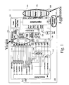
- Figure 1 shows a typical general architecture of a multiple-band 2G/3G phone 100 consisting of a quad band 2.75G (EGPRS), triple band 3G (HSPA+) with 3G receive diversity, comprising one single die 190, of a RF Front End circuit 110, a 2G/3G RF transceiver 120, a baseband 130, a PMU unit 140 and possibly DDR memory 150, being either external or internal, plus some additional components which are all listed below:
- RF Front-End circuitry 110 supports quad band 2G (Band II, III, V, VIII EGPRS), triple band 3G (WCDMA I, II, III) which is typical of recent mobile phone architecture, the selection of the particular mode/band being performed by means of an antenna switch 111 which directs the signal to the appropriate set of front end filters 112. Conversely, antenna switch 111 directs the transmit signal generated by the appropriate 2G or 3G Power amplifiers, respectively 113 and 114, to the antenna.
- 2/3G transceiver 120 includes the conventional circuits required for achieving a 2G or 3G mobile communication, such as, in the receiving chain, Low Noise amplifiers (LNA) 121, a Rx VCO Frequency synthesizer 122 with appropriate division circuits (represented by local divider LO Div), a circuit 123 achieving programmable Gain amplifier (PGA), Analog to digital converter (ADC) as well as DSP processing.
- LNA Low Noise amplifiers
- Rx VCO Frequency synthesizer 122 with appropriate division circuits (represented by local divider LO Div)
- PGA programmable Gain amplifier
- ADC Analog to digital converter
- transceiver 120 includes a circuit 126 achieving PGA, Digital to Analog (DAC) conversion as well as DSP processing, a Tx VCO frequency synthesizer 125 associated with dividing circuits (LO Div), and conventional digitally controlled Gain amplifier 124.
- DAC Digital to Analog
- Tx VCO frequency synthesizer 125 associated
- Transceiver 120 further includes appropriate timing circuits 126 as well as a RF-BB baseband interface 127 for interfacing the baseband 130.
- RFBBi_EN RX data 1, RX data 2, TX data 1, SYSCLKEN, SYSCLK
- SYSCLK SYSCLK
- baseband 130 achieves communication between the transceiver 120 (through interface 127) with different devices and peripherals, such as two cameras 160, two displays 170, a USB device 180 through appropriate data and control leads (including CLK clocks and Chip Select CSi) as well as external DDR memory.
- devices and peripherals such as two cameras 160, two displays 170, a USB device 180 through appropriate data and control leads (including CLK clocks and Chip Select CSi) as well as external DDR memory.
- PA Power Amplifier
- the present application particularly relates to the protection of the 2G receiver chain, identified in figure 1 as being the victim.
- the victim suffers from multiple sources of aggression which can be sorted into two categories:
- a first known solution consists in protecting the victim by carefully designing the LNA and systematically using differential wires in order to make best benefit of the common mode rejection of such a differential architectures.
- a second known solution is based on the use of sophisticated packages (eg. so-called flip chip package) for embodying the RF transceiver integrated circuit may reduce the coupling between the input wire of the LNA and the digital interface, which coupling generally increases with the frequency.
- sophisticated packages eg. so-called flip chip package
- control is based on the use of at least one programmable frequency divider
- control is performed by means of a general control unit (UCM) for the purpose of performing a contextual analysis of the current mode of operation of said wireless telecommunications and, in response to said contextual analysis, for determining the fine tuning of the clock rate to be applied to said component.
- UCM general control unit
- the general control unit - the Use Case Manager - uses one of the following information for determining said frequency :
- the individual component which is likely to desensitize the victim is one of the following: a memory storage, a display, a USB interface or a camera interface.
- the invention also achieves a wireless telecommunication apparatus comprising a RF transceiver for transmitting and receiving RF signals, a baseband comprising digital interface which are likely to desensitize said RF transceiver.
- the apparatus is characterized in that it further comprises means for performing an adaptive control on the clock rate of said component so as to locate a wideband noise PSD null just to the left or to the right, in the frequency domain, of the RF transceiver wanted carrier frequency (f w )
- the fine tuning of the clock rate of the component is achieved by means of at least one programmable frequency divider
- the apparatus includes a general control unit - a so called Use Case Manager - which performs a contextual analysis of the current mode of operation of said wireless telecommunications and, in response to said contextual analysis, for determining the fine tuning of the clock rate to be applied to said component.
- the invention is particularly suitable for achieving a 2G, 3G or LTE mobile phone incorporate highly sophisticated multimedia functionalities. Alternatively, it can be used for carrying out a Portable Document Assistant.
- clocking architecture which will be described is suitable for allowing combination of wide number of features and functions such as mentioned above, but can also be used for a limited subset of functionalities.
- each individual component identified as an aggressor in a mobile phone, has its own clock signal which is generated by one Phase Locked loops so that, in the whole phone, no less than 10 PLLs can be simultaneously (and asynchronously) operated, each one corresponding to its particular functional entity.
- the present invention brings a partial solution to the problem of wideband noise falling in the first category, which is generated by high speed data transfers between the single chip and its peripherals, such as camera, displays but also, USB and external memory interface (blocks 150, 160, 170, 180).
- the aggressor's frequency lobes result from the several high order harmonics of either the bit rate grid used to exchange data between the single chip I/O (input/output) pads and the external memory, or the external display(s), or the external camera(s), or even from the USB bus.
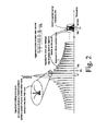
- Figure 2 shows the first power spectral density (PSD) properties of the first category of aggressor: wideband noise of a high speed data transfer on a serial or on a parallel interface, in the case of a high speed NRZ or RZ serial data link.
- PSD power spectral density
- the victim's carrier frequency denoted f w is located in between the N th harmonic null (or zero) and the N th +1 null of the aggressors PSD, thereby suffering from being jammed by the maximum PSD of the N th PSD lobe. It should be noticed that the data interface exhibits the spectrum of a pulsed clock spur leakage located at the frequency nulls of the data PSD.
- the digital high speed serial interfaces generate wideband spectral lobes which span over several hundred of MHz, which can couple directly into the LNA input pin(s) via electromagnetic coupling of the long bonding wires which can be modeled as radiating transmissions lines, acting in a fashion very similar to antennae.
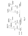
- FIG. 3a there is illustrated the severity of the problem for the case of a single chip GSM 900 RF /BB / PMU receiver which tends to be desensitized by the presence of the external memory interface wideband noise being clocked at 65 MHz (crosses) .
- the victim's carrier frequency is set to 937 MHz (channel 10). It can be seen that the victim is located within a maximum of the aggressor's 14 th lobe PSD.
- control is performed so as to set the aggressor wideband noise PSD null just to the left or to the right, in the frequency domain, of the victim's wanted carrier frequency denoted "f w ".
- the clocking rate of the individual aggressor(s) is/are defined by means of a central clocking system with a frequency plan being arranged so as to allow dynamic, reprogrammable scheme under control by the USM, in order to move the grid based upon the a-priori knowledge of the downlink wanted carrier frequency. This permits the victim to always take advantage of the lowest possible aggressor noise PSD and yet avoids the eventual strong pulsed clock leakage located at the exact frequency nulls of the the aggressor PSD.
- the adjustment of the particular clock rate of the one individual component - or aggressor - is achieved by means of at least one programmable frequency divider providing high resolution dividing ratio, based on the combination of integer divide ratios and fractional divide ratios for achieving fine adjustment of the clocking frequency
- the Use Case Manager UCM is arranged to have high-level vision of the contextual operations of the mobile telephone, and particularly any frequency switching of the RF transmitter controlled by the base station, so as to precisely generate the appropriate control parameters for controlling the different clocks required by the different elements
- the latter more particularly uses the following information for controlling the fine tuning of the clock rate:
- CM Use Case Manager
- the USM continuously performs a contextual analysis of the mode of operation of the mobile phone, taking into account a number of input parameters above, so as to precisely determine the control parameters used by the programmable dividers and, thus, fix the clock rate of the considered aggressor.
- the fine control of the clock rate of the memory is achieved by means of a central system clock generator PLL associated with a set of integer frequency dividers to derive multiple grids from a unique master clock source on which the external peripherals can be clocked to ensure evasion of the aggressor noise PSD.
- a central system clock generator PLL associated with a set of integer frequency dividers to derive multiple grids from a unique master clock source on which the external peripherals can be clocked to ensure evasion of the aggressor noise PSD.
- the unique system clock frequency is a multiple integer number of :
- Figure 5 illustrates one possible - and non limiting - embodiment of a clock architecture which can be used for providing accurate control of the frequency values for different aggressors.
- the architecture is based on at least one master clock reference, operating at f vco , for instance between 4 and 5 Ghz, and which can be used for generating all or most of the clocks used by the different constituents of the mobile phone, including the possible aggressors.
- PLL Phase Locked Loop
- oscillator 102 operating at f vco the output of which being connected to the input of a a programmable divider by N circuit 103 and which output is connected to the a first input of a phase comparator circuit 104, a second input of which receives the output of a 26 MHz reference crystal oscillator 105.
- this conventional PLL architecture may rely upon integer N or fractional N division ratios.
- the PLL comprising blocks 101, 102, 103, and 104 is used for generating all frequency clock references, particularly required by the baseband (or also entitled “CPU"), the memory (or also known as “DDR”) and display etc...
- the f vco frequency is divided by a programmable divider 106 which allows any division between N to N 1 so as to provide a so called variable Digital clock which can be further divided by a dedicated programmable divider 107 used for clocking the Digital Signal Processor (DSP) or also called “Central Processing Unit” (CPU) , as well as the divider 107 to feed the external DDR memory, the divider 109 to feed the camera interfaces etc...
- DSP Digital Signal Processor
- CPU Central Processing Unit
- programmable division ratios N1, N2 of divider 106, P1 of divider 107, P2 of divider 108 and P3 of divider 109 can be either implemented in integer N or as fractional division ratios depending on the mobile phone application (number of bands, number of telecommunication standards being supported, etc etc..).
- the architecture which is illustrated in figure 5 is only one illustrative example of how achieving one complete set of clocking signals which are derived from one single centralized master clock.
- the architecture can be adapted for the purpose of introducing some clock spreading techniques which are out of the scope of the present invention, but which may be advantageously used by the skilled man.
- the Use Case Manager is thus able to precisely define and control the clocking of each "aggressor", in accordance with the particular context of use of the mobile phone, including the Tx modulated carrier frequency, the Tx modulated carrier power, the DL received carrier power, the operating frequency band (DD & DG), the mode of operation (2G, 3G) , the clocking of the aggressor being considered.
- the PLL IS arranged so as to provide all clocks - high speed and low speed - which are required for embodying a recent mobile phone including a wide range of multimedia functionalities.
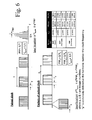
- Figure 6 illustrates, in the case of the memory, the determination of the position of the victim or RF carrier with respect to different possible situations:
- the spur location is generally defined by : p*f burst +/- q*PRF with q being an integer number
- the minimum frequency gap between the aggressor data PSD null and the location of the victim's carrier must be at least equal to p*f burst +PRF1+PRF2.
- the spur location is generally defined by : p*f burst +/- q*PRF1 +/- r*PRF2, where p, q & r are integer numbers, and "p" referring to the harmonic number of the clock frequency.
- Figure 6 also illustrates example of numerical values for 2 different categories of memories or aggressors, with the indication of the particular values for parameter PRF1 and PRF2.
- the invention which was described above achieves a very effective mitigation technique which prevents wideband data spectral lobes from falling within the downlink carrier frequency to which the UE is attached to in either Cell DCH state for 3G, or in connected mode for 2G systems.
Landscapes
- Engineering & Computer Science (AREA)
- Computer Networks & Wireless Communication (AREA)
- Signal Processing (AREA)
- Telephone Function (AREA)
- Mobile Radio Communication Systems (AREA)
- Transceivers (AREA)
- Noise Elimination (AREA)
Abstract
Particularly, the control is performed by means of the control of programmable frequency dividers, and under the control of a general control unit (UCM) for the purpose of performing a contextual analysis of the current mode of operation of said wireless telecommunications and, in response to said contextual analysis, for determining the fine tuning of the clock rate to be applied to said component.
Description
- The invention relates to the field of wireless communications and more particularly to a process and apparatus for reducing EMI in the RF subsystem of a wireless communication system.
- Until recently, mobile wireless equipment used separate Integrated Circuits (ICs) for the Radio Frequency (RF) transceiver, the baseband (BB) processor and the Power Management Unit (PMU). In the context of the permanent perpetual quest for cost reduction, the approach taken by most IC vendors is that of a single chip, made up of either a single RF CMOS die, or multiple separate dies, which integrates into a single package all three previously listed ICs, namely, RF, BB and PMU into a single package.
-
Figure 1 shows a typical general architecture of a multiple-band 2G/3G phone 100 consisting of a quad band 2.75G (EGPRS),triple band 3G (HSPA+) with 3G receive diversity, comprising onesingle die 190, of a RFFront End circuit 110, a 2G/3G RF transceiver 120, abaseband 130, aPMU unit 140 and possiblyDDR memory 150, being either external or internal, plus some additional components which are all listed below: - Label 110: mobile phone's RF front-end.
- Label 111: Antenna switch used for switching between different frequency bands.
- Label 112: 3G (HSPA) duplexer allows connection of the TX and RX path to the antenna switch and further achieves RF isolation between RF tx and RF rx chains.
- Label 113: 2.75 G (EGPRS) power amplifiers
- Label 114: 3G (HSPA) power amplifiers
- Label 115: Diversity receiver RF bandpass filters
- Label 190: Single die/single-chip RF (label 120)-BB(label 130)-PMU (label 140) IC.
- Label 120: Multi-standard, multi-band RF transmit/ receive (transceiver) IC.
- Label 130: Digital baseband (DBB) IC
- RF Front-
End circuitry 110 supportsquad band 2G (Band II, III, V, VIII EGPRS),triple band 3G (WCDMA I, II, III) which is typical of recent mobile phone architecture, the selection of the particular mode/band being performed by means of anantenna switch 111 which directs the signal to the appropriate set offront end filters 112. Conversely,antenna switch 111 directs the transmit signal generated by the appropriate 2G or 3G Power amplifiers, respectively 113 and 114, to the antenna. - 2/
3G transceiver 120 includes the conventional circuits required for achieving a 2G or 3G mobile communication, such as, in the receiving chain, Low Noise amplifiers (LNA) 121, a RxVCO Frequency synthesizer 122 with appropriate division circuits (represented by local divider LO Div), acircuit 123 achieving programmable Gain amplifier (PGA), Analog to digital converter (ADC) as well as DSP processing. On the transmitting chain,transceiver 120 includes acircuit 126 achieving PGA, Digital to Analog (DAC) conversion as well as DSP processing, a TxVCO frequency synthesizer 125 associated with dividing circuits (LO Div), and conventional digitally controlledGain amplifier 124.Transceiver 120 further includesappropriate timing circuits 126 as well as a RF-BB baseband interface 127 for interfacing thebaseband 130. For the sake of clarity, the different control, data and clock signals which are represented infigure 1 (such as RFBBi_EN,RX data 1,RX data 2,TX data 1, SYSCLKEN, SYSCLK) are conventional and known to the skilled man and do not need any further discussion. - Similarly,
baseband 130 achieves communication between the transceiver 120 (through interface 127) with different devices and peripherals, such as twocameras 160, two displays 170, aUSB device 180 through appropriate data and control leads (including CLK clocks and Chip Select CSi) as well as external DDR memory. - The integration of those components in a single die clearly reduces the cost of manufacturing a handset since the telecom pipe of the mobile phone now only requires very few extra additional components to make a phone call: one or several Power Amplifier(s) (PA) and its associated front-end circuitry such as RF bandpass filters, duplexers, antenna switch etc..
- However, despite the significant cost saving resulting from the use of a single RF-BB-PMU chip, some significant EMI problems need to be considered in order to prevent the RF receiver as well as the RF transmitter chain from being polluted by digital BB and external memory bus noise, as well as associated clock spurs, and their multiple harmonics.
- The present application particularly relates to the protection of the 2G receiver chain, identified in
figure 1 as being the victim. InFigure 1 , the victim suffers from multiple sources of aggression which can be sorted into two categories: - Wideband noise source aggressors: falls into this category, noise generated by high speed data transfers between the single chip and its peripherals, such as camera, displays but also, USB and external memory interface (
blocks - Narrowband spurs: falls into this category, either clock harmonics spurs, or pulsed clock source and their harmonics.
- Some solutions are known in the art for reducing the effects of such additional spurs.
- A first known solution consists in protecting the victim by carefully designing the LNA and systematically using differential wires in order to make best benefit of the common mode rejection of such a differential architectures.
- A second known solution is based on the use of sophisticated packages (eg. so-called flip chip package) for embodying the RF transceiver integrated circuit may reduce the coupling between the input wire of the LNA and the digital interface, which coupling generally increases with the frequency.
- All those techniques clearly tend to increase the design and manufacturing costs of the transceiver IC.
- In some situations, those techniques do not allow to avoid desensitization of the receiver in some circumstances. In particular, it has been shown that multiple integer harmonics of the reference clock used to transfer data over the external memory interface desensitize degrade an RF receiver.
- It is an object of the present invention to provide a new method for facilitating the cellular integration, particularly the digital (MCU/DSP) and one or more RF subsystem.
- It is another object of the present invention to provide a new wireless communication apparatus which allows simultaneous use of RF subsystem of a mobile phone, together with digital baseband operating in the same package while avoiding the desensitizing of the RF receiver located in the mobile phone.
- It is an object of the present invention to provide a new clocking architecture suitable for a mobile telephone offering multiple multimedia functionalities.
- It is a further object of the present invention to provide a new technique and method for defining the clock rate of individual component which are likely to generate wideband noise in one RF receiver, so as to minimize desensitization of the latter.
- These and other objects of the invention are achieved by means of method for dynamically clocking one component which is likely to desensitize a victim within the RF subsystem, such as the RF receiver for instance, comprising the step of performing an adaptive control on the clock rate of said component so as to locate a wideband noise PSD null just to the left or to the right, in the frequency domain, of the RF transceiver wanted carrier frequency (fw)
- In one embodiment, the control is based on the use of at least one programmable frequency divider
- Preferably, the control is performed by means of a general control unit (UCM) for the purpose of performing a contextual analysis of the current mode of operation of said wireless telecommunications and, in response to said contextual analysis, for determining the fine tuning of the clock rate to be applied to said component.
- In one particular embodiment, the general control unit - the Use Case Manager - uses one of the following information for determining said frequency :
- the RF receiver wanted carrier frequency;
- the RF receiver operating frequency band,
- the RF receiver operating mode (EGPRS, WCDMA etc...)
- the RF receiver wanted carrier received power
- the component activity: a priori knowledge of min and max values of Pulse Repetition Frequencies and fburst
- the component min/max clock frequency capabilities
- In one embodiment, the individual component which is likely to desensitize the victim is one of the following: a memory storage, a display, a USB interface or a camera interface.
- The invention also achieves a wireless telecommunication apparatus comprising a RF transceiver for transmitting and receiving RF signals, a baseband comprising digital interface which are likely to desensitize said RF transceiver.
- The apparatus is characterized in that it further comprises means for performing an adaptive control on the clock rate of said component so as to locate a wideband noise PSD null just to the left or to the right, in the frequency domain, of the RF transceiver wanted carrier frequency (fw)
- The fine tuning of the clock rate of the component is achieved by means of at least one programmable frequency divider
- In one embodiment, the apparatus includes a general control unit - a so called Use Case Manager - which performs a contextual analysis of the current mode of operation of said wireless telecommunications and, in response to said contextual analysis, for determining the fine tuning of the clock rate to be applied to said component.
- The invention is particularly suitable for achieving a 2G, 3G or LTE mobile phone incorporate highly sophisticated multimedia functionalities. Alternatively, it can be used for carrying out a Portable Document Assistant.
- Other features of one or more embodiments of the invention will best be understood by reference to the following detailed description when read in conjunction with the accompanying drawings.
-
Figure 1 shows an illustrative architecture of a mobile telephone including RF transceiver and different peripherals. -
Figure 2 shows the first power spectral density (PSD) properties of the first category of aggressor: wideband noise of a high speed data transfer on a serial or on a parallel interface -
Figures 3a illustrates the situation of asingle chip GSM 900 RF /BB / PMU receiver which shows to be desensitized by the presence of the external memory interface wideband noise being clocked at 65 MHz (crosses) -
Figures 3b illustrates the situation of asingle chip GSM 900 RF /BB / PMU receiver which shows to be desensitized by the presence of the external memory interface wideband noise being clocked at 78 MHz (crosses) -
Figure 4 illustrates one example of an arrangement of frequencies which are based on three independent references 19.2 Mhz, 26.0 Mhz and 38.4 Mhz. -
Figure 5 illustrates one embodiment of a clocking architecture which allows dynamic control of the modulated Tx clock spurs in accordance with one embodiment. -
Figure 6 illustrates in one example the determination of the spur location for different types of memory. - It will now be described how one can improve the integration of digital baseband systems and circuits with one or more RF subsystem. Clearly, the method and system being described hereinafter are particularly suitable for the purpose of designing an new mobile phone fitted with multimedia and enhanced functionalities, such as Global Positioning System (GPS), Bluetooth , wireless Ian, 2G and 3G, a high resolution camera and display(s) a TV out capability etc..
- Clearly, the clocking architecture which will be described is suitable for allowing combination of wide number of features and functions such as mentioned above, but can also be used for a limited subset of functionalities.
- Furthermore, it should be clear that the embodiments which will be described hereinafter should not be restricted to the telecommunication standards, nor to the frequency bands nor to the combination of bands which are shown in the illustrative example of
figure 1 . The technique described below can be used in a wide range of applications, and is particularly applicable to both 2G (EGPRS) systems and 3G systems (FDD-WCDMA all releases including Long Term Evolution), and can be advantageously incorporated in any recent architecture, such as typical architecture offigure 1 . - Conventionally, each individual component, identified as an aggressor in a mobile phone, has its own clock signal which is generated by one Phase Locked loops so that, in the whole phone, no less than 10 PLLs can be simultaneously (and asynchronously) operated, each one corresponding to its particular functional entity.
- The clocking of all those individual components - or aggressors - results, as mentioned in the first section of the present description, wideband noise which might contribute to desensitize the RF receiver.
- The present invention brings a partial solution to the problem of wideband noise falling in the first category, which is generated by high speed data transfers between the single chip and its peripherals, such as camera, displays but also, USB and external memory interface (
blocks - For such wideband noise, the aggressor's frequency lobes result from the several high order harmonics of either the bit rate grid used to exchange data between the single chip I/O (input/output) pads and the external memory, or the external display(s), or the external camera(s), or even from the USB bus.
-
Figure 2 shows the first power spectral density (PSD) properties of the first category of aggressor: wideband noise of a high speed data transfer on a serial or on a parallel interface, in the case of a high speed NRZ or RZ serial data link. - The victim's carrier frequency denoted fw is located in between the Nth harmonic null (or zero) and the Nth+1 null of the aggressors PSD, thereby suffering from being jammed by the maximum PSD of the Nth PSD lobe. It should be noticed that the data interface exhibits the spectrum of a pulsed clock spur leakage located at the frequency nulls of the data PSD.
- As shown in the figure, the digital high speed serial interfaces generate wideband spectral lobes which span over several hundred of MHz, which can couple directly into the LNA input pin(s) via electromagnetic coupling of the long bonding wires which can be modeled as radiating transmissions lines, acting in a fashion very similar to antennae.
- With respect to
Figure 3a , there is illustrated the severity of the problem for the case of asingle chip GSM 900 RF /BB / PMU receiver which tends to be desensitized by the presence of the external memory interface wideband noise being clocked at 65 MHz (crosses) . The victim's carrier frequency is set to 937 MHz (channel 10). It can be seen that the victim is located within a maximum of the aggressor's 14th lobe PSD. - In order to reduce desensitization of the RF receiver by the different possible aggressors, it is proposed to implement a fine and adaptive control of the clocking of each individual component or functional block which is identified as a possible aggressor for the considered victim, generally the RF receiver. This fine adaptive control is performed by a general control unit - a so-called Use Case Manager (UCM) - which has the function of adjusting, at a very fine level, the clock rate of the considered component so as to precisely position the aggressor wideband noise PSD with respect to the considered victim's carrier.
- In one embodiment, the control is performed so as to set the aggressor wideband noise PSD null just to the left or to the right, in the frequency domain, of the victim's wanted carrier frequency denoted "fw".
- It has been noticed that the fine adjustment of the null should not be exactly centered onto fw, because of the presence of interface clock leakage, but very close near that value.
- In any case, the skilled man will particularly define the best relative position of the victim's wanted carrier frequency "fw" with respect to the aggressor wideband noise PSD null
- In one particular embodiment, the clocking rate of the individual aggressor(s) is/are defined by means of a central clocking system with a frequency plan being arranged so as to allow dynamic, reprogrammable scheme under control by the USM, in order to move the grid based upon the a-priori knowledge of the downlink wanted carrier frequency. This permits the victim to always take advantage of the lowest possible aggressor noise PSD and yet avoids the eventual strong pulsed clock leakage located at the exact frequency nulls of the the aggressor PSD.
- In one embodiment, the adjustment of the particular clock rate of the one individual component - or aggressor - is achieved by means of at least one programmable frequency divider providing high resolution dividing ratio, based on the combination of integer divide ratios and fractional divide ratios for achieving fine adjustment of the clocking frequency
- By precisely adjusting the frequency clocking of the considered aggressor - such as the DDR storage for instance - one can ensure that the impact of wide band noise generated by external high speed data interface of the previously identified aggressors is being minimized within the RF receiver.
- In one particular embodiment, the Use Case Manager UCM is arranged to have high-level vision of the contextual operations of the mobile telephone, and particularly any frequency switching of the RF transmitter controlled by the base station, so as to precisely generate the appropriate control parameters for controlling the different clocks required by the different elements
- The latter more particularly uses the following information for controlling the fine tuning of the clock rate:
- victim's wanted carrier frequency (location of the victim in the frequency domain)
- victim's operating frequency band, and therefore a priori knowledge of duplex gap and duplex distance
- victim's operating mode (EGPRS, WCDMA etc...)
- victims's wanted carrier received power
- aggressor activity: a priori knowledge of min and max values of PRF1 and PRF2, and fburst
- aggressor min/max clock frequency capabilities (for eg. certain memories have tight tolerances on changing their operating clock frequencies)
- Indeed, considering for instance the case of the carrier received power, it has been noticed when the received power is very low - which is the case when the mobile phone is far away from its base station - a fine control of the clock rate shows to be very critical so as to avoid any desensitization of the RF receiver and, therefore, the Use Case Manager (CM) is aware of such information so as to perform very fine and effective control of the clock rate of the memory storage.
- To achieve the fine tuning of the clock rate of the aggressor, the USM continuously performs a contextual analysis of the mode of operation of the mobile phone, taking into account a number of input parameters above, so as to precisely determine the control parameters used by the programmable dividers and, thus, fix the clock rate of the considered aggressor.
- For the sake of clarity, there will now be considered one illustrative example of a
GSM900 channel 10 receiver victim and a new memory interface which is now clocked onto a 78 MHz grid instead of the previously shown 65 MHz grid. - Such illustrative example is shown in
Figure 3b . - It can be seen that not only does the victim benefit from the lowest aggressor noise PSD, but it is also protected from the strong clock leakage. The skilled man will straightforwardly adapt the teaching of the invention to not only other victim's carrier frequencies within this frequency band, but also to other frequency bands of the ETSI GSM standard. Note also that the technique also applies to other telecommunication standards than EGPRS. For example, but not limited to, this invention can be applied to any of the frequency bands of a WCDMA 3GPP standard modulated carrier.
- The fine control of the clock rate of the memory is achieved by means of a central system clock generator PLL associated with a set of integer frequency dividers to derive multiple grids from a unique master clock source on which the external peripherals can be clocked to ensure evasion of the aggressor noise PSD. To minimize cost and complexity, it is preferable, but not compulsory, that the unique system clock frequency is a multiple integer number of :
- The various crystal running frequencies, namely a multiple of 26 MHz and 19.2 MHz,
- Of the various interface data rates: for example 480 MHz for USB, 1248 MHz for M-PHY camera interfaces, etc..
- Clock candidates that fullfil these requirements are 1248 MHz, 2496MHz as shown in
Figure 4 illustrating a Master clock PLL source being the multiple integer of world's most used crystal frequencies: 26 and 19.2 MHz. It should be noticed that from 1248, the UMTS chip rate can be easily derived, as well as GSM, as well as LTE system clocks. USB 2.0 which uses 480 Mbit/s can also be derived since 1248 and 2496 are multiple integers of 24 MHz, and 480 MHz=24*20 MHz. -
Figure 5 illustrates one possible - and non limiting - embodiment of a clock architecture which can be used for providing accurate control of the frequency values for different aggressors. - The architecture is based on at least one master clock reference, operating at fvco, for instance between 4 and 5 Ghz, and which can be used for generating all or most of the clocks used by the different constituents of the mobile phone, including the possible aggressors.
- One sees a Phase Locked Loop (PLL) which is formed by means of
oscillator 102 operating at fvco the output of which being connected to the input of a a programmable divider byN circuit 103 and which output is connected to the a first input of aphase comparator circuit 104, a second input of which receives the output of a 26 MHzreference crystal oscillator 105. Note that this conventional PLL architecture may rely upon integer N or fractional N division ratios. - The
PLL comprising blocks programmable divider 106 which allows any division between N to N1 so as to provide a so called variable Digital clock which can be further divided by a dedicatedprogrammable divider 107 used for clocking the Digital Signal Processor (DSP) or also called "Central Processing Unit" (CPU) , as well as thedivider 107 to feed the external DDR memory, thedivider 109 to feed the camera interfaces etc... - Note that programmable division ratios N1, N2 of
divider 106, P1 ofdivider 107, P2 ofdivider 108 and P3 ofdivider 109 can be either implemented in integer N or as fractional division ratios depending on the mobile phone application (number of bands, number of telecommunication standards being supported, etc etc..). - It should be noticed that the architecture which is illustrated in
figure 5 is only one illustrative example of how achieving one complete set of clocking signals which are derived from one single centralized master clock. In particular, the architecture can be adapted for the purpose of introducing some clock spreading techniques which are out of the scope of the present invention, but which may be advantageously used by the skilled man. - It can be seen in
figure 5 that all the different clocks are under control of the Use Case Manager. This is represented by the control leads ofprogrammable dividers mutiplexors - Accordingly, the Use Case Manager is thus able to precisely define and control the clocking of each "aggressor", in accordance with the particular context of use of the mobile phone, including the Tx modulated carrier frequency, the Tx modulated carrier power, the DL received carrier power, the operating frequency band (DD & DG), the mode of operation (2G, 3G) , the clocking of the aggressor being considered.
- Basically, the PLL IS arranged so as to provide all clocks - high speed and low speed - which are required for embodying a recent mobile phone including a wide range of multimedia functionalities.
-
Figure 6 illustrates, in the case of the memory, the determination of the position of the victim or RF carrier with respect to different possible situations: - a. in the case of simple pulsed clock aggressors, the victim wanted carrier location in the frequency domain relative to the position of the data aggressor noise power spectral density null must be equal to the pulse repetition frequency (PRF = 1/T). fburst is equal to 1/T
- The spur location is generally defined by : p*fburst +/- q*PRF with q being an integer number
- b. In the case of aggressors using packet of pulsed clock, the minimum frequency gap between the aggressor data PSD null and the location of the victim's carrier must be at least equal to p*fburst+PRF1+PRF2.
- The spur location is generally defined by : p*fburst +/- q*PRF1 +/- r*PRF2, where p, q & r are integer numbers, and "p" referring to the harmonic number of the clock frequency.
-
Figure 6 also illustrates example of numerical values for 2 different categories of memories or aggressors, with the indication of the particular values for parameter PRF1 and PRF2. - As a conclusion, the invention which was described above achieves a very effective mitigation technique which prevents wideband data spectral lobes from falling within the downlink carrier frequency to which the UE is attached to in either Cell DCH state for 3G, or in connected mode for 2G systems.
Claims (15)
- Method for dynamically rocking one component located into a Wireless telecommunication apparatus comprising a RF transceiver subject to desensizitation by said component EMI, characterized in that it involves the steps of performing an adaptive control on the clock rate of said component so as to locate a wideband noise PSD null just to the left or to the right, in the frequency domain, of the RF transceiver wanted carrier frequency (fw)
- Method according to claim 1 characterized in that said control is based on the use of at least one programmable frequency divider.
- Method according to claim 1 or 2 characterized in that said control is performed by means of a general control unit (UCM) performing a contextual analysis of the current mode of operation of said wireless telecommunications and, in response to said contextual analysis, for determining the fine tuning of the clock rate to be applied to said component.
- Method according to claim 1 characterized in that said general control unit uses one of the following information for determining said frequency :- the RF transceiver wanted carrier frequency;- the RF transceiver operating frequency band,- the RF transceiver operating mode (EGPRS, WCDMA etc...)- the RF transceiver wanted carrier received power- the component activity, including a priori knowledge of min and max values of Pulse Repetition Frequencies (PRF1, PRF2) and fburst- the component min/max clock frequency capabilities
- A method according to anyone of claims 1 to 4 wherein said individual component is a memory storage, a display, a USB interface or a camera interface.
- A method according to anyone of claims 1 to 4 wherein a centralized master clock operates at a frequency between 4 and 5 Ghz.
- A method according to anyone of claims 1 to 4 wherein said centralized master clock drives a set of PLLs controlled by said central control unit.
- A wireless telecommunication apparatus comprising a RF transceiver subject to desensizitation by said component EMI, one component such as a baseband comprising digital interface which are likely to desensitize said RF transceiver; characterized in that it further comprises means for performing an adaptive control on the clock rate of said component so as to locate a wideband noise PSD null just to the left or to the right, in the frequency domain, of the RF transceiver wanted carrier frequency (fw)
- A wireless telecommunication apparatus according to claim 8 characterized in that said control is performed by means of the control of at least one programmable frequency divider
- A wireless telecommunication apparatus according to claim 8 or 9 further comprising a general control unit (UCM) for the purpose of performing a contextual analysis of the current mode of operation of said wireless telecommunications and, in response to said contextual analysis, for determining the fine tuning of the clock rate to be applied to said component.
- A wireless telecommunication apparatus according to claim 10 characterized in that said general control unit uses one of the following information for determining said frequency:- the RF transceiver wanted carrier frequency;- the RF transceiver operating frequency band,- the RF transceiver operating mode (EGPRS, WCDMA etc...)- the RF transceiver wanted carrier received power- the component activity, including a priori knowledge of min and max values of Pulse Repetition Frequencies (PRF1, PRF2) and fburst- the component min/max clock frequency capabilities
- A wireless telecommunication apparatus according to anyone of claims 8 to 11 wherein said individual component is a memory storage, a display, a USB interface or a camera interface.
- A wireless telecommunication apparatus according to anyone of claims 8 to 11 wherein a centralized master clock
- A wireless telecommunication apparatus according to anyone of claims 8 to 13 characterized in that it is embodied in a 2G or 3G or LTE mobile phone.
- A wireless telecommunication apparatus according to anyone of claims 8 to 13 characterized in that it is embodied in a Portable Assistant Document.
Priority Applications (4)
| Application Number | Priority Date | Filing Date | Title |
|---|---|---|---|
| EP10368010.4A EP2348652B1 (en) | 2010-01-26 | 2010-01-26 | Process and apparatus for reducing EMI in the RF subsystem of a wireless communication system |
| US13/574,965 US9059795B2 (en) | 2010-01-26 | 2011-01-26 | Process and apparatus for reducing EMI in the RF subsystem of a wireless communication system |
| PCT/EP2011/000347 WO2011092004A1 (en) | 2010-01-26 | 2011-01-26 | Process and apparatus for reducing emi in the rf subsystem of a wireless communication system |
| KR1020127019709A KR101795090B1 (en) | 2010-01-26 | 2011-01-26 | Process and apparatus for reducing emi in the rf subsystem of a wireless communication system |
Applications Claiming Priority (1)
| Application Number | Priority Date | Filing Date | Title |
|---|---|---|---|
| EP10368010.4A EP2348652B1 (en) | 2010-01-26 | 2010-01-26 | Process and apparatus for reducing EMI in the RF subsystem of a wireless communication system |
Publications (2)
| Publication Number | Publication Date |
|---|---|
| EP2348652A1 true EP2348652A1 (en) | 2011-07-27 |
| EP2348652B1 EP2348652B1 (en) | 2016-08-10 |
Family
ID=42272376
Family Applications (1)
| Application Number | Title | Priority Date | Filing Date |
|---|---|---|---|
| EP10368010.4A Not-in-force EP2348652B1 (en) | 2010-01-26 | 2010-01-26 | Process and apparatus for reducing EMI in the RF subsystem of a wireless communication system |
Country Status (4)
| Country | Link |
|---|---|
| US (1) | US9059795B2 (en) |
| EP (1) | EP2348652B1 (en) |
| KR (1) | KR101795090B1 (en) |
| WO (1) | WO2011092004A1 (en) |
Cited By (1)
| Publication number | Priority date | Publication date | Assignee | Title |
|---|---|---|---|---|
| WO2015038658A1 (en) * | 2013-09-13 | 2015-03-19 | Qualcomm Incorporated | Dynamic frequency plan |
Families Citing this family (4)
| Publication number | Priority date | Publication date | Assignee | Title |
|---|---|---|---|---|
| JP6449568B2 (en) * | 2014-06-24 | 2019-01-09 | 京セラ株式会社 | Mobile terminal and control method |
| US9584209B2 (en) * | 2014-12-31 | 2017-02-28 | Nxp B. V. | Multiple antenna distributed radio system |
| KR102530073B1 (en) | 2016-07-15 | 2023-05-08 | 삼성전자주식회사 | Baseband Integrated Circuit for communicating with RF Integrated Circuit using digital interface And Apparatus including the same |
| US20200076488A1 (en) | 2018-08-30 | 2020-03-05 | Skyworks Solutions, Inc. | Beamforming communication systems with sensor aided beam management |
Citations (3)
| Publication number | Priority date | Publication date | Assignee | Title |
|---|---|---|---|---|
| WO1996037978A1 (en) * | 1995-05-23 | 1996-11-28 | Microunity Systems Engineering, Inc. | Noise reduction in integrated circuits and circuit assemblies |
| US20050255881A1 (en) * | 2004-05-17 | 2005-11-17 | Shinya Yamamoto | Portable telephone apparatus with camera |
| US20090138745A1 (en) * | 2007-11-26 | 2009-05-28 | John Gregory Dorsey | Electronic devices with radio-frequency collision resolution capabilities |
Family Cites Families (5)
| Publication number | Priority date | Publication date | Assignee | Title |
|---|---|---|---|---|
| US20040239415A1 (en) * | 2003-05-27 | 2004-12-02 | Bishop Christopher Brent | Methods of predicting power spectral density of a modulated signal and of a multi-h continuous phase modulated signal |
| ATE422732T1 (en) * | 2004-09-06 | 2009-02-15 | Freescale Semiconductor Inc | WIRELESS COMMUNICATION DEVICE AND DATA INTERFACE |
| AR060699A1 (en) * | 2006-04-26 | 2008-07-10 | Qualcomm Inc | ENERGY SCHEME OF THE WORK CYCLE |
| US7804377B2 (en) * | 2006-10-21 | 2010-09-28 | Mnemonics, Inc. | Apparatus and method for producing an SBPSK-type modulated signal using piecewise linear phase transition shaping |
| US8239694B2 (en) * | 2008-03-31 | 2012-08-07 | Qualcomm, Incorporated | Dynamic frequency scaling of a switched mode power supply |
-
2010
- 2010-01-26 EP EP10368010.4A patent/EP2348652B1/en not_active Not-in-force
-
2011
- 2011-01-26 US US13/574,965 patent/US9059795B2/en active Active
- 2011-01-26 WO PCT/EP2011/000347 patent/WO2011092004A1/en not_active Ceased
- 2011-01-26 KR KR1020127019709A patent/KR101795090B1/en not_active Expired - Fee Related
Patent Citations (3)
| Publication number | Priority date | Publication date | Assignee | Title |
|---|---|---|---|---|
| WO1996037978A1 (en) * | 1995-05-23 | 1996-11-28 | Microunity Systems Engineering, Inc. | Noise reduction in integrated circuits and circuit assemblies |
| US20050255881A1 (en) * | 2004-05-17 | 2005-11-17 | Shinya Yamamoto | Portable telephone apparatus with camera |
| US20090138745A1 (en) * | 2007-11-26 | 2009-05-28 | John Gregory Dorsey | Electronic devices with radio-frequency collision resolution capabilities |
Cited By (2)
| Publication number | Priority date | Publication date | Assignee | Title |
|---|---|---|---|---|
| WO2015038658A1 (en) * | 2013-09-13 | 2015-03-19 | Qualcomm Incorporated | Dynamic frequency plan |
| US20150079909A1 (en) * | 2013-09-13 | 2015-03-19 | Qualcomm Incorporated | Dynamic frequency plan |
Also Published As
| Publication number | Publication date |
|---|---|
| WO2011092004A1 (en) | 2011-08-04 |
| KR101795090B1 (en) | 2017-12-01 |
| US9059795B2 (en) | 2015-06-16 |
| EP2348652B1 (en) | 2016-08-10 |
| US20130122958A1 (en) | 2013-05-16 |
| KR20120140646A (en) | 2012-12-31 |
Similar Documents
| Publication | Publication Date | Title |
|---|---|---|
| EP2348642B1 (en) | Process for achieving spur mitigation in an integrated circuit including a wide band receiver | |
| US8755751B2 (en) | Wireless communication apparatus having modulated Tx clock spur control | |
| US8724649B2 (en) | Distributed coexistence system for interference mitigation in a single chip radio or multi-radio communication device | |
| US8548104B2 (en) | Receiver with configurable clock frequencies | |
| US8891679B2 (en) | Polar transmitter suitable for monolithic integration in SoCs | |
| WO2016023002A1 (en) | Front end architecture for intermittent emissions and/or coexistence specifications | |
| US9059795B2 (en) | Process and apparatus for reducing EMI in the RF subsystem of a wireless communication system | |
| TWI693806B (en) | Wireless communication device with coexistence of multiple wireless communication systems | |
| CN113098549B (en) | Harmonic rejection local oscillator signal generation | |
| EP1792410B1 (en) | Wireless communication device and data interface | |
| CN104243376B (en) | Communicator and associated method | |
| US20140051365A1 (en) | Method and device for sending signals between a radio frequency circuit and a baseband circuit | |
| EP2811670B1 (en) | Interference suppression method and apparatus | |
| US12395178B2 (en) | Partial-fractional phase-locked loop with sigma delta modulator and finite impulse response filter | |
| US20250266981A1 (en) | Mitigating digital interference within radio frequency circuitry | |
| Friedman et al. | Coexistence performance enhancement techniques for DRP based WLAN/WPAN and cellular radios collocated in a mobile device | |
| US20070186125A1 (en) | Electronic circuit and method for operating an electronic circuit | |
| HK1233778A1 (en) | Front end architecture for intermittent emissions and/or coexistence specifications |
Legal Events
| Date | Code | Title | Description |
|---|---|---|---|
| PUAI | Public reference made under article 153(3) epc to a published international application that has entered the european phase |
Free format text: ORIGINAL CODE: 0009012 |
|
| AK | Designated contracting states |
Kind code of ref document: A1 Designated state(s): AT BE BG CH CY CZ DE DK EE ES FI FR GB GR HR HU IE IS IT LI LT LU LV MC MK MT NL NO PL PT RO SE SI SK SM TR |
|
| AX | Request for extension of the european patent |
Extension state: AL BA RS |
|
| 17P | Request for examination filed |
Effective date: 20120127 |
|
| 17Q | First examination report despatched |
Effective date: 20120309 |
|
| GRAP | Despatch of communication of intention to grant a patent |
Free format text: ORIGINAL CODE: EPIDOSNIGR1 |
|
| INTG | Intention to grant announced |
Effective date: 20160218 |
|
| GRAS | Grant fee paid |
Free format text: ORIGINAL CODE: EPIDOSNIGR3 |
|
| GRAA | (expected) grant |
Free format text: ORIGINAL CODE: 0009210 |
|
| AK | Designated contracting states |
Kind code of ref document: B1 Designated state(s): AT BE BG CH CY CZ DE DK EE ES FI FR GB GR HR HU IE IS IT LI LT LU LV MC MK MT NL NO PL PT RO SE SI SK SM TR |
|
| REG | Reference to a national code |
Ref country code: GB Ref legal event code: FG4D |
|
| REG | Reference to a national code |
Ref country code: CH Ref legal event code: EP Ref country code: AT Ref legal event code: REF Ref document number: 819884 Country of ref document: AT Kind code of ref document: T Effective date: 20160815 |
|
| REG | Reference to a national code |
Ref country code: IE Ref legal event code: FG4D |
|
| REG | Reference to a national code |
Ref country code: DE Ref legal event code: R096 Ref document number: 602010035319 Country of ref document: DE |
|
| REG | Reference to a national code |
Ref country code: LT Ref legal event code: MG4D |
|
| REG | Reference to a national code |
Ref country code: NL Ref legal event code: MP Effective date: 20160810 |
|
| REG | Reference to a national code |
Ref country code: FR Ref legal event code: PLFP Year of fee payment: 8 |
|
| REG | Reference to a national code |
Ref country code: DE Ref legal event code: R081 Ref document number: 602010035319 Country of ref document: DE Owner name: OCT CIRCUIT TECHNOLOGIES INTERNATIONAL LTD., IE Free format text: FORMER OWNER: ST-ERICSSON SA, PLAN-LES-OUATES, CH |
|
| REG | Reference to a national code |
Ref country code: AT Ref legal event code: MK05 Ref document number: 819884 Country of ref document: AT Kind code of ref document: T Effective date: 20160810 |
|
| RAP2 | Party data changed (patent owner data changed or rights of a patent transferred) |
Owner name: OCT CIRCUIT TECHNOLOGIES INTERNATIONAL LIMITED |
|
| PG25 | Lapsed in a contracting state [announced via postgrant information from national office to epo] |
Ref country code: NL Free format text: LAPSE BECAUSE OF FAILURE TO SUBMIT A TRANSLATION OF THE DESCRIPTION OR TO PAY THE FEE WITHIN THE PRESCRIBED TIME-LIMIT Effective date: 20160810 Ref country code: LT Free format text: LAPSE BECAUSE OF FAILURE TO SUBMIT A TRANSLATION OF THE DESCRIPTION OR TO PAY THE FEE WITHIN THE PRESCRIBED TIME-LIMIT Effective date: 20160810 Ref country code: IS Free format text: LAPSE BECAUSE OF FAILURE TO SUBMIT A TRANSLATION OF THE DESCRIPTION OR TO PAY THE FEE WITHIN THE PRESCRIBED TIME-LIMIT Effective date: 20161210 Ref country code: NO Free format text: LAPSE BECAUSE OF FAILURE TO SUBMIT A TRANSLATION OF THE DESCRIPTION OR TO PAY THE FEE WITHIN THE PRESCRIBED TIME-LIMIT Effective date: 20161110 Ref country code: HR Free format text: LAPSE BECAUSE OF FAILURE TO SUBMIT A TRANSLATION OF THE DESCRIPTION OR TO PAY THE FEE WITHIN THE PRESCRIBED TIME-LIMIT Effective date: 20160810 Ref country code: IT Free format text: LAPSE BECAUSE OF FAILURE TO SUBMIT A TRANSLATION OF THE DESCRIPTION OR TO PAY THE FEE WITHIN THE PRESCRIBED TIME-LIMIT Effective date: 20160810 Ref country code: FI Free format text: LAPSE BECAUSE OF FAILURE TO SUBMIT A TRANSLATION OF THE DESCRIPTION OR TO PAY THE FEE WITHIN THE PRESCRIBED TIME-LIMIT Effective date: 20160810 |
|
| PG25 | Lapsed in a contracting state [announced via postgrant information from national office to epo] |
Ref country code: ES Free format text: LAPSE BECAUSE OF FAILURE TO SUBMIT A TRANSLATION OF THE DESCRIPTION OR TO PAY THE FEE WITHIN THE PRESCRIBED TIME-LIMIT Effective date: 20160810 Ref country code: GR Free format text: LAPSE BECAUSE OF FAILURE TO SUBMIT A TRANSLATION OF THE DESCRIPTION OR TO PAY THE FEE WITHIN THE PRESCRIBED TIME-LIMIT Effective date: 20161111 Ref country code: LV Free format text: LAPSE BECAUSE OF FAILURE TO SUBMIT A TRANSLATION OF THE DESCRIPTION OR TO PAY THE FEE WITHIN THE PRESCRIBED TIME-LIMIT Effective date: 20160810 Ref country code: SE Free format text: LAPSE BECAUSE OF FAILURE TO SUBMIT A TRANSLATION OF THE DESCRIPTION OR TO PAY THE FEE WITHIN THE PRESCRIBED TIME-LIMIT Effective date: 20160810 Ref country code: PL Free format text: LAPSE BECAUSE OF FAILURE TO SUBMIT A TRANSLATION OF THE DESCRIPTION OR TO PAY THE FEE WITHIN THE PRESCRIBED TIME-LIMIT Effective date: 20160810 Ref country code: PT Free format text: LAPSE BECAUSE OF FAILURE TO SUBMIT A TRANSLATION OF THE DESCRIPTION OR TO PAY THE FEE WITHIN THE PRESCRIBED TIME-LIMIT Effective date: 20161212 Ref country code: AT Free format text: LAPSE BECAUSE OF FAILURE TO SUBMIT A TRANSLATION OF THE DESCRIPTION OR TO PAY THE FEE WITHIN THE PRESCRIBED TIME-LIMIT Effective date: 20160810 |
|
| PG25 | Lapsed in a contracting state [announced via postgrant information from national office to epo] |
Ref country code: RO Free format text: LAPSE BECAUSE OF FAILURE TO SUBMIT A TRANSLATION OF THE DESCRIPTION OR TO PAY THE FEE WITHIN THE PRESCRIBED TIME-LIMIT Effective date: 20160810 Ref country code: EE Free format text: LAPSE BECAUSE OF FAILURE TO SUBMIT A TRANSLATION OF THE DESCRIPTION OR TO PAY THE FEE WITHIN THE PRESCRIBED TIME-LIMIT Effective date: 20160810 |
|
| REG | Reference to a national code |
Ref country code: DE Ref legal event code: R097 Ref document number: 602010035319 Country of ref document: DE |
|
| PG25 | Lapsed in a contracting state [announced via postgrant information from national office to epo] |
Ref country code: SM Free format text: LAPSE BECAUSE OF FAILURE TO SUBMIT A TRANSLATION OF THE DESCRIPTION OR TO PAY THE FEE WITHIN THE PRESCRIBED TIME-LIMIT Effective date: 20160810 Ref country code: CZ Free format text: LAPSE BECAUSE OF FAILURE TO SUBMIT A TRANSLATION OF THE DESCRIPTION OR TO PAY THE FEE WITHIN THE PRESCRIBED TIME-LIMIT Effective date: 20160810 Ref country code: DK Free format text: LAPSE BECAUSE OF FAILURE TO SUBMIT A TRANSLATION OF THE DESCRIPTION OR TO PAY THE FEE WITHIN THE PRESCRIBED TIME-LIMIT Effective date: 20160810 Ref country code: BG Free format text: LAPSE BECAUSE OF FAILURE TO SUBMIT A TRANSLATION OF THE DESCRIPTION OR TO PAY THE FEE WITHIN THE PRESCRIBED TIME-LIMIT Effective date: 20161110 Ref country code: SK Free format text: LAPSE BECAUSE OF FAILURE TO SUBMIT A TRANSLATION OF THE DESCRIPTION OR TO PAY THE FEE WITHIN THE PRESCRIBED TIME-LIMIT Effective date: 20160810 Ref country code: BE Free format text: LAPSE BECAUSE OF FAILURE TO SUBMIT A TRANSLATION OF THE DESCRIPTION OR TO PAY THE FEE WITHIN THE PRESCRIBED TIME-LIMIT Effective date: 20160810 |
|
| PLBE | No opposition filed within time limit |
Free format text: ORIGINAL CODE: 0009261 |
|
| STAA | Information on the status of an ep patent application or granted ep patent |
Free format text: STATUS: NO OPPOSITION FILED WITHIN TIME LIMIT |
|
| 26N | No opposition filed |
Effective date: 20170511 |
|
| PG25 | Lapsed in a contracting state [announced via postgrant information from national office to epo] |
Ref country code: SI Free format text: LAPSE BECAUSE OF FAILURE TO SUBMIT A TRANSLATION OF THE DESCRIPTION OR TO PAY THE FEE WITHIN THE PRESCRIBED TIME-LIMIT Effective date: 20160810 |
|
| REG | Reference to a national code |
Ref country code: CH Ref legal event code: PL |
|
| PG25 | Lapsed in a contracting state [announced via postgrant information from national office to epo] |
Ref country code: MC Free format text: LAPSE BECAUSE OF FAILURE TO SUBMIT A TRANSLATION OF THE DESCRIPTION OR TO PAY THE FEE WITHIN THE PRESCRIBED TIME-LIMIT Effective date: 20160810 |
|
| PG25 | Lapsed in a contracting state [announced via postgrant information from national office to epo] |
Ref country code: CH Free format text: LAPSE BECAUSE OF NON-PAYMENT OF DUE FEES Effective date: 20170131 Ref country code: LI Free format text: LAPSE BECAUSE OF NON-PAYMENT OF DUE FEES Effective date: 20170131 |
|
| REG | Reference to a national code |
Ref country code: IE Ref legal event code: MM4A |
|
| PG25 | Lapsed in a contracting state [announced via postgrant information from national office to epo] |
Ref country code: LU Free format text: LAPSE BECAUSE OF NON-PAYMENT OF DUE FEES Effective date: 20170126 |
|
| REG | Reference to a national code |
Ref country code: FR Ref legal event code: PLFP Year of fee payment: 9 |
|
| PG25 | Lapsed in a contracting state [announced via postgrant information from national office to epo] |
Ref country code: IE Free format text: LAPSE BECAUSE OF NON-PAYMENT OF DUE FEES Effective date: 20170126 |
|
| PG25 | Lapsed in a contracting state [announced via postgrant information from national office to epo] |
Ref country code: MT Free format text: LAPSE BECAUSE OF NON-PAYMENT OF DUE FEES Effective date: 20170126 |
|
| PG25 | Lapsed in a contracting state [announced via postgrant information from national office to epo] |
Ref country code: HU Free format text: LAPSE BECAUSE OF FAILURE TO SUBMIT A TRANSLATION OF THE DESCRIPTION OR TO PAY THE FEE WITHIN THE PRESCRIBED TIME-LIMIT; INVALID AB INITIO Effective date: 20100126 |
|
| PG25 | Lapsed in a contracting state [announced via postgrant information from national office to epo] |
Ref country code: CY Free format text: LAPSE BECAUSE OF NON-PAYMENT OF DUE FEES Effective date: 20160810 |
|
| PG25 | Lapsed in a contracting state [announced via postgrant information from national office to epo] |
Ref country code: MK Free format text: LAPSE BECAUSE OF FAILURE TO SUBMIT A TRANSLATION OF THE DESCRIPTION OR TO PAY THE FEE WITHIN THE PRESCRIBED TIME-LIMIT Effective date: 20160810 |
|
| PG25 | Lapsed in a contracting state [announced via postgrant information from national office to epo] |
Ref country code: TR Free format text: LAPSE BECAUSE OF FAILURE TO SUBMIT A TRANSLATION OF THE DESCRIPTION OR TO PAY THE FEE WITHIN THE PRESCRIBED TIME-LIMIT Effective date: 20160810 |
|
| REG | Reference to a national code |
Ref country code: GB Ref legal event code: 732E Free format text: REGISTERED BETWEEN 20210722 AND 20210728 |
|
| REG | Reference to a national code |
Ref country code: GB Ref legal event code: 732E Free format text: REGISTERED BETWEEN 20210805 AND 20210811 |
|
| PGFP | Annual fee paid to national office [announced via postgrant information from national office to epo] |
Ref country code: FR Payment date: 20230125 Year of fee payment: 14 |
|
| PGFP | Annual fee paid to national office [announced via postgrant information from national office to epo] |
Ref country code: GB Payment date: 20230127 Year of fee payment: 14 Ref country code: DE Payment date: 20230127 Year of fee payment: 14 |
|
| REG | Reference to a national code |
Ref country code: DE Ref legal event code: R119 Ref document number: 602010035319 Country of ref document: DE |
|
| GBPC | Gb: european patent ceased through non-payment of renewal fee |
Effective date: 20240126 |
|
| PG25 | Lapsed in a contracting state [announced via postgrant information from national office to epo] |
Ref country code: DE Free format text: LAPSE BECAUSE OF NON-PAYMENT OF DUE FEES Effective date: 20240801 |
|
| PG25 | Lapsed in a contracting state [announced via postgrant information from national office to epo] |
Ref country code: GB Free format text: LAPSE BECAUSE OF NON-PAYMENT OF DUE FEES Effective date: 20240126 |
|
| PG25 | Lapsed in a contracting state [announced via postgrant information from national office to epo] |
Ref country code: FR Free format text: LAPSE BECAUSE OF NON-PAYMENT OF DUE FEES Effective date: 20240131 |
|
| PG25 | Lapsed in a contracting state [announced via postgrant information from national office to epo] |
Ref country code: GB Free format text: LAPSE BECAUSE OF NON-PAYMENT OF DUE FEES Effective date: 20240126 Ref country code: FR Free format text: LAPSE BECAUSE OF NON-PAYMENT OF DUE FEES Effective date: 20240131 Ref country code: DE Free format text: LAPSE BECAUSE OF NON-PAYMENT OF DUE FEES Effective date: 20240801 |