EP2348529A2 - Organic light-emitting diode display apparatus and method of manufacturing the same - Google Patents
Organic light-emitting diode display apparatus and method of manufacturing the same Download PDFInfo
- Publication number
- EP2348529A2 EP2348529A2 EP11151596A EP11151596A EP2348529A2 EP 2348529 A2 EP2348529 A2 EP 2348529A2 EP 11151596 A EP11151596 A EP 11151596A EP 11151596 A EP11151596 A EP 11151596A EP 2348529 A2 EP2348529 A2 EP 2348529A2
- Authority
- EP
- European Patent Office
- Prior art keywords
- display apparatus
- pdl
- oled display
- electrodes
- layer
- Prior art date
- Legal status (The legal status is an assumption and is not a legal conclusion. Google has not performed a legal analysis and makes no representation as to the accuracy of the status listed.)
- Ceased
Links
- 238000004519 manufacturing process Methods 0.000 title claims abstract description 9
- 239000010409 thin film Substances 0.000 claims abstract description 6
- 239000010410 layer Substances 0.000 claims description 105
- 239000000758 substrate Substances 0.000 claims description 24
- 229920000642 polymer Polymers 0.000 claims description 23
- VYPSYNLAJGMNEJ-UHFFFAOYSA-N Silicium dioxide Chemical compound O=[Si]=O VYPSYNLAJGMNEJ-UHFFFAOYSA-N 0.000 claims description 16
- 238000000034 method Methods 0.000 claims description 13
- -1 A12O3 Inorganic materials 0.000 claims description 11
- 229910004205 SiNX Inorganic materials 0.000 claims description 7
- 229910052681 coesite Inorganic materials 0.000 claims description 7
- 229910052906 cristobalite Inorganic materials 0.000 claims description 7
- 239000000377 silicon dioxide Substances 0.000 claims description 7
- 229910052682 stishovite Inorganic materials 0.000 claims description 7
- 229910052905 tridymite Inorganic materials 0.000 claims description 7
- URLKBWYHVLBVBO-UHFFFAOYSA-N Para-Xylene Chemical group CC1=CC=C(C)C=C1 URLKBWYHVLBVBO-UHFFFAOYSA-N 0.000 claims description 6
- UMIVXZPTRXBADB-UHFFFAOYSA-N benzocyclobutene Chemical compound C1=CC=C2CCC2=C1 UMIVXZPTRXBADB-UHFFFAOYSA-N 0.000 claims description 6
- ZKATWMILCYLAPD-UHFFFAOYSA-N niobium pentoxide Chemical compound O=[Nb](=O)O[Nb](=O)=O ZKATWMILCYLAPD-UHFFFAOYSA-N 0.000 claims description 6
- 239000004952 Polyamide Substances 0.000 claims description 5
- 239000012044 organic layer Substances 0.000 claims description 5
- 229920002647 polyamide Polymers 0.000 claims description 5
- GWEVSGVZZGPLCZ-UHFFFAOYSA-N Titan oxide Chemical compound O=[Ti]=O GWEVSGVZZGPLCZ-UHFFFAOYSA-N 0.000 claims description 4
- MCMNRKCIXSYSNV-UHFFFAOYSA-N Zirconium dioxide Chemical compound O=[Zr]=O MCMNRKCIXSYSNV-UHFFFAOYSA-N 0.000 claims description 4
- 229920003229 poly(methyl methacrylate) Polymers 0.000 claims description 4
- 239000004926 polymethyl methacrylate Substances 0.000 claims description 4
- 229910052814 silicon oxide Inorganic materials 0.000 claims description 4
- KXGFMDJXCMQABM-UHFFFAOYSA-N 2-methoxy-6-methylphenol Chemical compound [CH]OC1=CC=CC([CH])=C1O KXGFMDJXCMQABM-UHFFFAOYSA-N 0.000 claims description 3
- ATVJXMYDOSMEPO-UHFFFAOYSA-N 3-prop-2-enoxyprop-1-ene Chemical compound C=CCOCC=C ATVJXMYDOSMEPO-UHFFFAOYSA-N 0.000 claims description 3
- 229910016553 CuOx Inorganic materials 0.000 claims description 3
- IMROMDMJAWUWLK-UHFFFAOYSA-N Ethenol Chemical compound OC=C IMROMDMJAWUWLK-UHFFFAOYSA-N 0.000 claims description 3
- YCKRFDGAMUMZLT-UHFFFAOYSA-N Fluorine atom Chemical compound [F] YCKRFDGAMUMZLT-UHFFFAOYSA-N 0.000 claims description 3
- 239000004642 Polyimide Substances 0.000 claims description 3
- 150000001408 amides Chemical class 0.000 claims description 3
- 239000011737 fluorine Substances 0.000 claims description 3
- 229910052731 fluorine Inorganic materials 0.000 claims description 3
- 150000003949 imides Chemical class 0.000 claims description 3
- 239000005011 phenolic resin Substances 0.000 claims description 3
- 229920001568 phenolic resin Polymers 0.000 claims description 3
- 229920001721 polyimide Polymers 0.000 claims description 3
- 239000004793 Polystyrene Substances 0.000 claims description 2
- 229910052454 barium strontium titanate Inorganic materials 0.000 claims description 2
- CJNBYAVZURUTKZ-UHFFFAOYSA-N hafnium(IV) oxide Inorganic materials O=[Hf]=O CJNBYAVZURUTKZ-UHFFFAOYSA-N 0.000 claims description 2
- 229910052451 lead zirconate titanate Inorganic materials 0.000 claims description 2
- ISWSIDIOOBJBQZ-UHFFFAOYSA-N phenol group Chemical group C1(=CC=CC=C1)O ISWSIDIOOBJBQZ-UHFFFAOYSA-N 0.000 claims description 2
- PBCFLUZVCVVTBY-UHFFFAOYSA-N tantalum pentoxide Inorganic materials O=[Ta](=O)O[Ta](=O)=O PBCFLUZVCVVTBY-UHFFFAOYSA-N 0.000 claims description 2
- 229920000740 poly(D-lysine) polymer Polymers 0.000 claims 19
- 239000003990 capacitor Substances 0.000 description 10
- PXHVJJICTQNCMI-UHFFFAOYSA-N Nickel Chemical compound [Ni] PXHVJJICTQNCMI-UHFFFAOYSA-N 0.000 description 9
- 239000011651 chromium Substances 0.000 description 8
- 229910052804 chromium Inorganic materials 0.000 description 7
- 229910052759 nickel Inorganic materials 0.000 description 7
- 239000011368 organic material Substances 0.000 description 7
- 239000000203 mixture Substances 0.000 description 6
- 229910052782 aluminium Inorganic materials 0.000 description 5
- 229910052779 Neodymium Inorganic materials 0.000 description 4
- 229910052791 calcium Inorganic materials 0.000 description 4
- 229910052737 gold Inorganic materials 0.000 description 4
- 229910052741 iridium Inorganic materials 0.000 description 4
- 229910052744 lithium Inorganic materials 0.000 description 4
- 229910052749 magnesium Inorganic materials 0.000 description 4
- 229910052751 metal Inorganic materials 0.000 description 4
- 239000002184 metal Substances 0.000 description 4
- 229910052763 palladium Inorganic materials 0.000 description 4
- 229910052697 platinum Inorganic materials 0.000 description 4
- 229910052709 silver Inorganic materials 0.000 description 4
- 229910045601 alloy Inorganic materials 0.000 description 3
- 239000000956 alloy Substances 0.000 description 3
- 238000001505 atmospheric-pressure chemical vapour deposition Methods 0.000 description 3
- 150000001875 compounds Chemical class 0.000 description 3
- 239000004020 conductor Substances 0.000 description 3
- 239000002019 doping agent Substances 0.000 description 3
- 239000011229 interlayer Substances 0.000 description 3
- 238000004518 low pressure chemical vapour deposition Methods 0.000 description 3
- 239000011159 matrix material Substances 0.000 description 3
- 229910052750 molybdenum Inorganic materials 0.000 description 3
- 238000002161 passivation Methods 0.000 description 3
- 238000000623 plasma-assisted chemical vapour deposition Methods 0.000 description 3
- 238000004528 spin coating Methods 0.000 description 3
- YTPLMLYBLZKORZ-UHFFFAOYSA-N Thiophene Chemical compound C=1C=CSC=1 YTPLMLYBLZKORZ-UHFFFAOYSA-N 0.000 description 2
- QVGXLLKOCUKJST-UHFFFAOYSA-N atomic oxygen Chemical compound [O] QVGXLLKOCUKJST-UHFFFAOYSA-N 0.000 description 2
- 238000005530 etching Methods 0.000 description 2
- PJXISJQVUVHSOJ-UHFFFAOYSA-N indium(III) oxide Inorganic materials [O-2].[O-2].[O-2].[In+3].[In+3] PJXISJQVUVHSOJ-UHFFFAOYSA-N 0.000 description 2
- 238000002347 injection Methods 0.000 description 2
- 239000007924 injection Substances 0.000 description 2
- 238000007641 inkjet printing Methods 0.000 description 2
- 229910010272 inorganic material Inorganic materials 0.000 description 2
- 239000011147 inorganic material Substances 0.000 description 2
- 239000011810 insulating material Substances 0.000 description 2
- PQXKHYXIUOZZFA-UHFFFAOYSA-M lithium fluoride Inorganic materials [Li+].[F-] PQXKHYXIUOZZFA-UHFFFAOYSA-M 0.000 description 2
- 239000011572 manganese Substances 0.000 description 2
- 239000000463 material Substances 0.000 description 2
- 229910052760 oxygen Inorganic materials 0.000 description 2
- 239000001301 oxygen Substances 0.000 description 2
- 230000035515 penetration Effects 0.000 description 2
- 229920000767 polyaniline Polymers 0.000 description 2
- 229910021420 polycrystalline silicon Inorganic materials 0.000 description 2
- 235000012239 silicon dioxide Nutrition 0.000 description 2
- 239000010936 titanium Substances 0.000 description 2
- 239000012780 transparent material Substances 0.000 description 2
- 229910052721 tungsten Inorganic materials 0.000 description 2
- 239000004925 Acrylic resin Substances 0.000 description 1
- 229920000178 Acrylic resin Polymers 0.000 description 1
- OKTJSMMVPCPJKN-UHFFFAOYSA-N Carbon Chemical compound [C] OKTJSMMVPCPJKN-UHFFFAOYSA-N 0.000 description 1
- VYZAMTAEIAYCRO-UHFFFAOYSA-N Chromium Chemical compound [Cr] VYZAMTAEIAYCRO-UHFFFAOYSA-N 0.000 description 1
- 229910001374 Invar Inorganic materials 0.000 description 1
- XEEYBQQBJWHFJM-UHFFFAOYSA-N Iron Chemical compound [Fe] XEEYBQQBJWHFJM-UHFFFAOYSA-N 0.000 description 1
- PWHULOQIROXLJO-UHFFFAOYSA-N Manganese Chemical compound [Mn] PWHULOQIROXLJO-UHFFFAOYSA-N 0.000 description 1
- ZOKXTWBITQBERF-UHFFFAOYSA-N Molybdenum Chemical compound [Mo] ZOKXTWBITQBERF-UHFFFAOYSA-N 0.000 description 1
- 229910052581 Si3N4 Inorganic materials 0.000 description 1
- RTAQQCXQSZGOHL-UHFFFAOYSA-N Titanium Chemical compound [Ti] RTAQQCXQSZGOHL-UHFFFAOYSA-N 0.000 description 1
- 230000002745 absorbent Effects 0.000 description 1
- 239000002250 absorbent Substances 0.000 description 1
- 229910021417 amorphous silicon Inorganic materials 0.000 description 1
- 230000004888 barrier function Effects 0.000 description 1
- 229910052799 carbon Inorganic materials 0.000 description 1
- 238000005229 chemical vapour deposition Methods 0.000 description 1
- 239000011248 coating agent Substances 0.000 description 1
- 238000000576 coating method Methods 0.000 description 1
- 238000000151 deposition Methods 0.000 description 1
- 238000009792 diffusion process Methods 0.000 description 1
- 239000010408 film Substances 0.000 description 1
- 239000011888 foil Substances 0.000 description 1
- 239000011521 glass Substances 0.000 description 1
- 230000005525 hole transport Effects 0.000 description 1
- 229910001026 inconel Inorganic materials 0.000 description 1
- 150000002500 ions Chemical class 0.000 description 1
- 229910000833 kovar Inorganic materials 0.000 description 1
- 239000002346 layers by function Substances 0.000 description 1
- 239000007788 liquid Substances 0.000 description 1
- 229910052748 manganese Inorganic materials 0.000 description 1
- 239000007769 metal material Substances 0.000 description 1
- 239000011733 molybdenum Substances 0.000 description 1
- 230000002093 peripheral effect Effects 0.000 description 1
- 229920003023 plastic Polymers 0.000 description 1
- 229920002098 polyfluorene Polymers 0.000 description 1
- 238000007639 printing Methods 0.000 description 1
- 230000002940 repellent Effects 0.000 description 1
- 239000005871 repellent Substances 0.000 description 1
- 238000007789 sealing Methods 0.000 description 1
- HQVNEWCFYHHQES-UHFFFAOYSA-N silicon nitride Chemical compound N12[Si]34N5[Si]62N3[Si]51N64 HQVNEWCFYHHQES-UHFFFAOYSA-N 0.000 description 1
- 238000004544 sputter deposition Methods 0.000 description 1
- 239000010935 stainless steel Substances 0.000 description 1
- 229910001220 stainless steel Inorganic materials 0.000 description 1
- 229930192474 thiophene Natural products 0.000 description 1
- 229910052719 titanium Inorganic materials 0.000 description 1
- 238000010023 transfer printing Methods 0.000 description 1
- TVIVIEFSHFOWTE-UHFFFAOYSA-K tri(quinolin-8-yloxy)alumane Chemical compound [Al+3].C1=CN=C2C([O-])=CC=CC2=C1.C1=CN=C2C([O-])=CC=CC2=C1.C1=CN=C2C([O-])=CC=CC2=C1 TVIVIEFSHFOWTE-UHFFFAOYSA-K 0.000 description 1
- WFKWXMTUELFFGS-UHFFFAOYSA-N tungsten Chemical compound [W] WFKWXMTUELFFGS-UHFFFAOYSA-N 0.000 description 1
- 239000010937 tungsten Substances 0.000 description 1
Images



Classifications
-
- H—ELECTRICITY
- H10—SEMICONDUCTOR DEVICES; ELECTRIC SOLID-STATE DEVICES NOT OTHERWISE PROVIDED FOR
- H10K—ORGANIC ELECTRIC SOLID-STATE DEVICES
- H10K59/00—Integrated devices, or assemblies of multiple devices, comprising at least one organic light-emitting element covered by group H10K50/00
- H10K59/10—OLED displays
- H10K59/12—Active-matrix OLED [AMOLED] displays
- H10K59/122—Pixel-defining structures or layers, e.g. banks
-
- H—ELECTRICITY
- H10—SEMICONDUCTOR DEVICES; ELECTRIC SOLID-STATE DEVICES NOT OTHERWISE PROVIDED FOR
- H10K—ORGANIC ELECTRIC SOLID-STATE DEVICES
- H10K2102/00—Constructional details relating to the organic devices covered by this subclass
- H10K2102/301—Details of OLEDs
- H10K2102/351—Thickness
Definitions
- the invention relates to an organic light-emitting diode (OLED) display apparatus and a method of manufacturing the same, and more particularly, to an OLED display apparatus including pixels having uniform thicknesses and a method of manufacturing the same.
- OLED organic light-emitting diode
- An organic light-emitting diode (OLED) display apparatus is classified as passive matrix (PM) and active matrix (AM) type OLED display apparatus according to its driving method.
- PM type OLED (PM-OLED) display apparatus anodes and cathodes are arrayed in a plurality of columns and a plurality of rows.
- the cathodes are supplied with scanning signals from a row driving circuit.
- a data signal is input into each pixel from a column driving circuit.
- the AM type OLED (AM-OLED) display apparatus controls a signal input into each pixel using a thin film transistor (TFT) and is appropriate for processing a large number of signals.
- TFT thin film transistor
- a passivation layer is formed on the TFT of the AM-OLED display apparatus to passivate the TFT and as a planarizing layer for planarizing an upper surface of the TFT.
- Pixel-defining layers are formed on the passivation layer.
- the PDLs are formed to be thick to prevent colour mixtures among pixels, the thicknesses of emission parts formed among the PDLs vary. If thin PDLs are formed to solve these colour mixtures, an upper surface of the TFT area underneath the thin PDLs is not planarized.
- the present embodiments aim to overcome the above problems as well as providing additional advantages.
- the present embodiments provide an organic light-emitting diode (OLED) display apparatus in which a thickness of an emission area is uniform and an upper surface of thin film transistor (TFT) area is planarized and a method of manufacturing the OLED display apparatus.
- OLED organic light-emitting diode
- an organic light-emitting diode (OLED) display apparatus including: thin film transistor (TFT) which is formed on a substrate; first electrode which is formed on a planarizing layer in each pixel, wherein the planarizing layer covers the TFT; pixel-defining layers (PDLs) which includes first PDL covering an end of the first electrode and second PDL exposing an end of the first PDL and covering the first PDL; intermediate layer which is formed on the first electrode and includes an emission layer (EML); and second electrode which is positioned opposite to the first electrode.
- TFT thin film transistor
- PDLs pixel-defining layers
- EML emission layer
- an organic light-emitting diode (OLED) display apparatus including: forming over a substrate first electrodes in each pixel; forming first PDLs covering ends of the first electrodes; forming second PDLs exposing ends of the first PDLs and covering the first PDLs; and forming intermediate layers including EMLs on the first electrodes; and forming second electrodes opposite to the first electrodes.
- OLED organic light-emitting diode
- the second PDL may be formed on the first PDL to bury uneven parts formed on a planarizing layer.
- the first PDLs may be formed of inorganic layers.
- the first PDLs may be formed of at least one of SiO 2 , SiN x , A1 2 O 3 , CuO x , Tb 4 O 7 , Y 2 O 3 , Nb 2 O 5 , and Pr 2 O 3 , for example.
- Each of the first PDLs may be formed to a thickness of from about 0.1 ⁇ m to about 1 ⁇ m.
- the second PDLs may include organic layers.
- the second PDLs may be formed of one selected from the group consisting of polyacryl, polyimide, polyamide (PA), benzocyclobutene (BCB), and phenolic resin.
- Each of the second PDLs may have a thickness from about 0.1 ⁇ m to about 2 ⁇ m in a direction in which different colour pixels are arrayed, and a thickness between 0.1 ⁇ m and 1 ⁇ m in a direction in which equal colour pixels are arrayed.
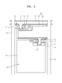
- FIG. 1 is a schematic plan view of a pixel electrode part of an organic light-emitting diode (OLED) display apparatus according to an embodiment.
- FIG. 2 is an enlarged plan view of a pixel of the OLED display apparatus of FIG. 1 .
- the OLED display apparatus includes a display area in which red (R), green (G), and blue (B) pixels are repeatedly arrayed.
- the R, G, and B pixels are repeatedly arrayed in stripe patterns in columns and rows but the present embodiments are not limited thereto.
- the R, G, and B pixels may be arrayed in zigzag patterns in which pixels in each row are misaligned, matrix patterns, or the like.
- a part of the display area is illustrated for convenience, the R, G, and B pixels are repeatedly arrayed in direction A-A', and the same colour pixels are repeatedly arrayed in direction B-B'.
- Each of the R, G, and B pixels includes a selective driving circuit, which has thin film transistors (TFTs) 30 and 40, a capacitor 50, and the like, and an OLED 60.
- TFTs thin film transistors
- Each of the R, G, and B pixels includes a data line 72, a gate line 71, and a power source line 73 that is a driving power source of the OLED 60.
- the TFTs 30 and 40 respectively are a switching TFT and a driving TFT (hereinafter the TFTs 30 and 40 will be respectively referred to as the switching TFT 30 and the driving TFT 40).
- the switching TFT 30 is driven by a scan signal applied to the gate line 71 to transmit a data signal applied to the data line 72.
- the driving TFT 40 determines an amount of current flowing into the OLED 60 according to the data signal transmitted through the switching TFT 30 e.g., a voltage difference between a gate and a source.
- the capacitor 50 stores the data signal transmitted through the switching TFT 30 for a frame.
- a source electrode 31 of the switching TFT 30 is connected to the selective driving circuit through the data line 72, and a gate electrode 32 of the switching TFT 30 is connected to another driving circuit (not shown) through the gate line 71.
- a drain electrode 33 of the switching TFT 30 is connected to a first capacitor electrode 51 of the capacitor 50 and a gate electrode 43 of the driving TFT 40.
- a second capacitor electrode 52 of the capacitor 50 and a source electrode 47 of the driving TFT 40 are connected to the power source line 73, and a drain electrode 45 of the driving TFT 40 is connected to a first electrode 61 of the OLED 60.
- the number of TFTs and capacitors of the selective driving circuit is not limited thereto, and the selective driving circuit may include a larger number of TFTs and a larger number of capacitors.
- the OLED 60 includes the first electrode 61, which is a pixel electrode, and a second electrode (not shown) which is a common electrode and opposite the first electrode at a predetermined gap from the first electrode 61.
- An intermediate layer (not shown) including an organic emission layer (OEML) intervenes between the first electrode 61 and the second electrode to emit light by the first electrode 61 and the second electrode.
- OEML organic emission layer
- a pixel-defining layer (PDL) 81 is formed around an end of the first electrode 61 of the OLED 60.
- the PDL 81 includes a first PDL 81a, which is an inorganic layer, and a second PDL 81b, which is an organic layer.
- the first PDL 81a is formed to cover the end of the first electrode 61
- the second PDL 81b is formed on the first PDL 81a to expose an end of the first PDL 81a.
- FIG. 3 is a schematic cross-sectional view of an OLED display apparatus according to another embodiment.
- the OLED display apparatus includes a plurality of TFTs 40 and a plurality of OLEDs 60 which are formed on a substrate 10.
- Each TFT 40 includes active layer 41, gate electrode 43, and source and drain electrodes 45 and 47.
- a gate insulating layer 13 intervenes between the gate electrode 43 and the active layer 41 to insulate the gate electrode 43 from the active layer 41.
- the active layer 41 includes source and drain regions and a channel region. Here, a high-density dopant has been injected into both ends of each of the source and drain regions, and the channel region is formed between the source and drain regions. The source and drain regions are respectively connected to the source/drain electrodes 45 and 47.
- Each OLED 60 includes a first electrode 61, a second electrode 65, and an intermediate layer 63 intervening between the first and second electrodes 61 and 65.
- the first electrode 61 is formed on a passivation layer 17 in each pixel and connected to one of the source/drain electrodes 45 and 47 of the TFTs 40 through via holes H1.
- the PDLs 81 are formed around ends of the first electrodes 61 to define the pixels.
- the PDLs 81 include first PDLs 81a and second PDLs 81b.
- Each of the first PDLs 81a is formed of an inorganic layer.
- the first PDLs 81a are formed between adjacent two first electrodes 61 and cover the ends of the first electrodes 61.
- Each of the second PDLs 81b is formed of organic layer on the first PDL 81a to cover steep slope region P in which the end of the first electrode 61 and the via hole H1 is formed.
- the edge of second PDL 81b is positioned at predetermined distance from edge of the first PDL 81a. Distances between edges of the first and second PDLs 81a and 81b may be about 1 ⁇ m or less and may be determined in consideration of aperture ratio and emission effective region of the first electrode 61.
- Thicknesses of the first PDLs 81a may be each set to from about 0.1 ⁇ m to about 1 ⁇ m.
- Thicknesses of the second PDL 81b may be each set to from about 0.1 ⁇ m to about 2 ⁇ m in the direction A-A' of FIG. 1 to prevent colour mixtures among adjacent R, G, and B pixels. And thickness of the second PDL 81b may be set to from about 0.1 ⁇ m to about 1 ⁇ m in the direction B-B' of FIG. 1 to minimize step differences of the OEMLs.
- the first PDLs 81a are formed of an inorganic material having similar surface energy to that of the intermediate layers 63 stacked on the first electrodes 61.
- the second PDLs 81b are formed of an organic material having different surface energy from that of the intermediate layers 63.
- the PDL is formed, and a surface of the PDL is processed using a liquid repellent to prevent colour mixtures among pixels in order to form OEML using an ink jet or nozzle printing method.
- a liquid repellent to prevent colour mixtures among pixels in order to form OEML using an ink jet or nozzle printing method.
- the PDLs are formed thick, thicknesses of the centre of a pixel and the end of the pixel meeting the PDL are different from each other.
- the PDL is formed thin, surface curves of lower TFT area formed by uneven parts such as steep slope regions P or cracks A are not sufficiently planarized, wherein a via hole is formed in the steep slope region P, and the cracks A are formed in an etching process.
- moisture, oxygen, or the like penetrates into the PDL, and shorts may occur between the first and second electrodes 61 and 65.
- the first PDLs 81a having thin thicknesses are formed around the end of the first electrode 61, and the second PDL 81b is formed at predetermined distance from the edge of the first PDL 81.
- the second PDLs 81b are formed on the first PDLs 81a in which uneven parts such as cracks or the like are formed, to improve step coverage in order to planarize lower TFT area and minimize short between the first and second electrodes 61 and 65.
- the second PDLs 81b are formed on the first PDLs 81a, except on the ends of the first PDLs 81a.
- the second PDLs 81b may be additionally formed in the uneven parts such as the steep slope regions P or the cracks A.
- TFTs and three capacitors are shown in FIG. 3 but the present embodiment is not limited thereto. Thus, at least one TFT and at least one capacitor may be formed.
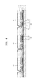
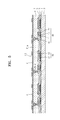
- FIGS. 4 through 6 are schematic cross-sectional views illustrating a method of manufacturing an OLED display apparatus, according to an embodiment.
- the present embodiment exemplifies an OLED display apparatus having a stripe structure in which the same colour pixels are arrayed in column directions, and R, G, and B pixels are repeatedly arrayed in row directions from left to right.
- TFTs 40 and first electrodes 61 are formed above a substrate 10.
- the substrate 10 may be formed of a transparent glass material including SiO2 as a main component but is not limited thereto. That is, the substrate 10 may be formed of a transparent plastic material, a metallic material, or the like.
- the substrate 10 is formed of a transparent material. If the OLED display apparatus is a top-emission type display apparatus which realizes an image in an opposite direction to the substrate 10, the substrate 10 does not need to be formed of a transparent material.
- the substrate 10 may be formed of metal. If the substrate 10 is formed of the metal, the substrate 10 may include at least one or more selected from the group consisting of carbon (C), iron (Fe), chromium (Cr), manganese (Mn), nickel (Ni), titanium (Ti), molybdenum (Mo), stainless steel (SUS), an Invar alloy, an Inconel alloy, and a Kovar alloy.
- the substrate 10 is not limited thereto and may be formed of a metal foil.
- An insulating layer 11 is formed on an upper surface of the substrate 10 to prevent diffusion of dopant ions and penetration of moisture or air and function and for planarizing the upper surface of the substrate 10 as a barrier layer and/or a buffer layer.
- the insulating layer 11 may be formed of SiO2 and/or silicon nitride (SiNx) using a plasma enhanced chemical vapor deposition (PECVD) method, an atmospheric pressure CVD (APCVD) method, a low pressure CVD (LPCVD) method, or the like.
- PECVD plasma enhanced chemical vapor deposition
- APCVD atmospheric pressure CVD
- LPCVD low pressure CVD
- Active layers 41 of the TFTs 40 are formed on the insulating layer 11.
- amorphous silicon may be deposited and crystallized on the insulating layer 11 to form a polycrystalline silicon layer (not shown), and the polycrystalline silicon layer may be patterned.
- Each active layer 41 of the TFTs 40 includes source and/or drain regions and channel region.
- Each active layer 41 has the source and drain regions at ends of the active layer 41 corresponding to sides of gate electrode 43 by doped with N-type or p-type dopants.
- the channel region is formed between the source and drain regions.
- a gate insulating layer 13 is formed on the active layers 41 of the TFTs 40.
- the gate insulating layer 13 may be formed of an inorganic material such as SiNx or silicon oxide (SiOx) using a PECVD method, an APCVD method, an LPCVD method, or the like.
- the gate electrodes 43 are formed partially on the gate insulating layer 13, and an interlayer insulating layer 15 is formed to cover the gate electrodes 43.
- the gate electrodes 43 may be formed of various types of conductive materials such as Al, Mo, tungsten (W), Cr, Ni, or a compound of Al, Mo, W, Cr, and Ni. If light is to pass through the active layers 41 of the TFTs 40 and other elements, the gate electrodes 43 may be formed of various types of transparent conductive materials such as ITO, IZO, or the like.
- Source/drain electrodes 45 and 47 are formed on the interlayer insulating layer 15 and connected to the active layers 41 through contact holes formed in the interlayer insulating layer 15.
- a planarizing layer 17 is formed on the source/drain electrodes 45 and 47.
- the planarizing layer 17 may be an inorganic insulating layer and/or an organic insulating layer.
- the inorganic insulating layer may include SiO 2 , SiN x , SiON, A1 2 O 3 , TiO 2 , Ta 2 O 5 , HfO 2 , ZrO 2 , BST, PZT, or the like.
- the organic insulating layer may include commercial polymer such as polymethyl methacrylate (PMMA), polystyrene (PS), or the like, polymeric derivative having a phenol group, acryl-based polymer, imide-based polymer, allylether-based polymer, amide-based polymer, fluorine-based polymer, p-xylene-based polymer, vinyl alcohol-based polymer, or a blend of commercial polymer, polymeric derivative, acryl-based polymer, imide-based polymer, allylether-based polymer,amide-based polymer, fluorine-based polymer, p-xylene-based polymer, and vinyl alcohol-based polymer.
- the planarizing layer 17 may have a complex stack structure of an inorganic insulating layer and an organic insulating layer.
- Stack structures of TFTs as described above are not limited thereto, and TFTs having various types of structures may be used.
- the present embodiment exemplifies top gate type TFTs, but different types of TFTs may be formed.
- the first electrodes 61 are formed on the planarizing layer 17 as pixel electrodes of an OLED and are electrically connected to one of the source/drain electrodes 45 and 47 through via holes H1.
- the via holes H1 are formed by etching the planarizing layer 17 and exposing the source/drain electrodes 45 and 47.
- the first electrodes 61 may be formed of various types of conductive materials in each pixel. If the OLED display apparatus is a bottom-emission type display apparatus which realizes an image toward the substrate 10, the first electrodes 61 may be transparent electrodes and may be formed of ITO, IZO, ZnO, or In 2 O 3 for example, having a high work function. If the OLED display apparatus is a top-emission type display apparatus which realizes an image in an opposite direction to the substrate 10, the first electrodes 61 may be reflective electrodes.
- a reflective layer may be formed of Ag, Mg, Al, Pt, Pd, Au, Ni, Nd, Ir, Cr, Li, Ca, or a compound of Ag, Mg, A1, Pt, Pd, Au, Ni, Nd, Ir, Cr, Li, and Ca, and ITO, IZO, ZnO, or In 2 O 3 , for example, having a high work function may be formed on the reflective layer in order to form the first electrodes 61.
- first PDLs 81a are formed to cover ends of the first electrodes 61.
- an inorganic insulating layer is deposited on a whole surface of the substrate 10 above which the first electrodes 61 have been formed, and patterned using a photolithographic process, to form openings H2 which expose central parts of the first electrodes 61.
- the inorganic insulating layer may be formed of one or more inorganic insulating materials selected from SiO 2 , SiN x , A1 2 O 3 , CuO x , Tb 4 O 7 , Y 2 O 3 , Nb 2 O 5 , Pr 2 O 3 , and the like using a sputtering method, a CVD method, a deposition method, or the like.
- the first PDLs 81a may be each formed to a thickness between about 0.1 ⁇ m and 1 ⁇ m to minimize differences in thicknesses of OEMLs between ends and central parts of the first electrodes 61.
- second PDLs 81b are formed on the first PDLs 81a.
- An organic insulating layer is deposited on the whole surface of the substrate 10 above which the first PDLs 81a have been formed, and then patterned using a photolithographic process, to form openings H3 so as to expose central parts of the first electrode 61 and ends of the first PDLs 81a.
- the organic insulating layer may be formed of one or more organic insulating materials selected from the group consisting of polyimide, polyamide, acrylic resin, benzocyclobutene (BCB), and phenolic resin using spin coating, slot coating, or the like.
- Thicknesses of the second PDLs 81b may be each set to a range between about 0.1 ⁇ m and 2 ⁇ m in row directions to prevent colour mixtures among adjacent R, G, and B pixels and a range between about 0.1 ⁇ m and 1 ⁇ m in column directions to minimize step differences in the thicknesses of the OEMLs.
- a gap between edges of the first and second PDLs 81a and 81b around the end of the first electrode 61 may be about 1 ⁇ m.
- the second PDLs 81b are formed on the first PDLs 81a to bury the cracks in order to improve step coverage and prevent penetration of air and shorts between electrodes.
- the intermediate layers 63 including the OEMLs and the second electrodes 65 are formed in openings through which first electrodes 61 are exposed.
- the intermediate layers 63 may be formed in a single or complex stack structure of one or more of functional layers including an emissive layer (EML), a hole transport layer (HTL), a hole injection layer (HIL), an electron transport layer (ETL), and an electron injection layer (EIL).
- EML emissive layer
- HTL hole transport layer
- HIL hole injection layer
- ETL electron transport layer
- EIL electron injection layer
- the intermediate layers 63 may be formed of a low or high molecular weight organic material.
- the HTL and the HIL are stacked toward the first electrodes 61 based on the OEMLs, and the ETL and the EIL are stacked toward the second electrodes 65 in order form the intermediate layers 63.
- Other types of layers may be stacked in order to form the intermediate layers 63.
- the low molecular weight organic material may be CuPC, NPB, Alq 3 , or the like.
- the intermediate layers 63 may include only the HTL toward the first electrodes 61 with respect to the OEMLs.
- the HTL may be formed of poly-(2,4)-ethylene-dihydroxy thiophene (PEDOT), polyaniline (PANI), or the like on the first electrodes 61 using ink jet printing, spin coating, or the like.
- the high molecular weight organic material may be a PPV-based or polyfluorene-based high molecular weight organic material.
- Colour patterns may be formed using a normal method such as ink jet printing, spin coating, thermal transfer printing using a laser, or the like, in order to form the intermediate layers 63.
- the second electrodes 65 may be deposited above the whole surface of the substrate 10 and may be formed as common electrodes.
- the first electrodes 61 are used as anode electrodes
- the second electrodes 65 are used as cathode electrodes.
- the present embodiments are not limited thereto and the polarities of the first electrodes 61 and the second electrodes 65 may be the opposite.
- the first electrodes 61 are transparent electrodes
- the second electrodes 65 are reflective electrodes.
- a metal having a low work function for example, Ag, Mg, Al, Pt, Pd, Au, Ni, Nd, Ir, Cr, Li, Ca, LiF/Ca, LiF/Al, or a compound of Ag, Mg, Al, Pt, Pd, Au, Ni, Nd, Ir, Cr, Li, Ca, LiF/Ca, and LiF/Al, for example, may be thinly deposited to form the reflective electrodes.
- a sealing member (not shown) and a moisture absorbent may be further formed on the second electrodes 65 to protect the OEMLs from external moisture or oxygen.
- an OLED display apparatus includes PDLs formed of inorganic and organic insulating layers.
- PDLs formed of inorganic and organic insulating layers.
Landscapes
- Engineering & Computer Science (AREA)
- Microelectronics & Electronic Packaging (AREA)
- Electroluminescent Light Sources (AREA)
- Devices For Indicating Variable Information By Combining Individual Elements (AREA)
Abstract
Description
- The invention relates to an organic light-emitting diode (OLED) display apparatus and a method of manufacturing the same, and more particularly, to an OLED display apparatus including pixels having uniform thicknesses and a method of manufacturing the same.
- An organic light-emitting diode (OLED) display apparatus is classified as passive matrix (PM) and active matrix (AM) type OLED display apparatus according to its driving method. In the PM type OLED (PM-OLED) display apparatus, anodes and cathodes are arrayed in a plurality of columns and a plurality of rows. Thus, the cathodes are supplied with scanning signals from a row driving circuit. Here, only one of the plurality of rows is selected. Also, a data signal is input into each pixel from a column driving circuit. The AM type OLED (AM-OLED) display apparatus controls a signal input into each pixel using a thin film transistor (TFT) and is appropriate for processing a large number of signals. Thus, the AM-OLED display apparatus is mainly used as a display apparatus for realizing a moving picture.
- A passivation layer is formed on the TFT of the AM-OLED display apparatus to passivate the TFT and as a planarizing layer for planarizing an upper surface of the TFT. Pixel-defining layers (PDLs) are formed on the passivation layer.
- If the PDLs are formed to be thick to prevent colour mixtures among pixels, the thicknesses of emission parts formed among the PDLs vary. If thin PDLs are formed to solve these colour mixtures, an upper surface of the TFT area underneath the thin PDLs is not planarized. The present embodiments aim to overcome the above problems as well as providing additional advantages.
- The present embodiments provide an organic light-emitting diode (OLED) display apparatus in which a thickness of an emission area is uniform and an upper surface of thin film transistor (TFT) area is planarized and a method of manufacturing the OLED display apparatus.
- According to an aspect of the present embodiments, there is provided an organic light-emitting diode (OLED) display apparatus including: thin film transistor (TFT) which is formed on a substrate; first electrode which is formed on a planarizing layer in each pixel, wherein the planarizing layer covers the TFT; pixel-defining layers (PDLs) which includes first PDL covering an end of the first electrode and second PDL exposing an end of the first PDL and covering the first PDL; intermediate layer which is formed on the first electrode and includes an emission layer (EML); and second electrode which is positioned opposite to the first electrode.
- According to another aspect of the present embodiments, there is provided a method of manufacturing an organic light-emitting diode (OLED) display apparatus, including: forming over a substrate first electrodes in each pixel; forming first PDLs covering ends of the first electrodes; forming second PDLs exposing ends of the first PDLs and covering the first PDLs; and forming intermediate layers including EMLs on the first electrodes; and forming second electrodes opposite to the first electrodes.
- The second PDL may be formed on the first PDL to bury uneven parts formed on a planarizing layer.
- The first PDLs may be formed of inorganic layers. The first PDLs may be formed of at least one of SiO2, SiNx, A12O3, CuOx, Tb4O7, Y2O3, Nb2O5, and Pr2O3, for example.
- Each of the first PDLs may be formed to a thickness of from about 0.1µm to about 1µm.
- The second PDLs may include organic layers. The second PDLs may be formed of one selected from the group consisting of polyacryl, polyimide, polyamide (PA), benzocyclobutene (BCB), and phenolic resin.
- Each of the second PDLs may have a thickness from about 0.1µm to about 2 µm in a direction in which different colour pixels are arrayed, and a thickness between 0.1µm and 1µm in a direction in which equal colour pixels are arrayed.
- The above and other features and advantages of the present embodiments will become more apparent by describing in detail exemplary embodiments thereof with reference to the attached drawings in which:
-
FIG. 1 is a schematic plan view of a pixel electrode part of an organic light-emitting diode (OLED) display apparatus according to an embodiment; -
FIG. 2 is an enlarged plan view of a pixel of OLED display apparatus ofFIG. 1 ; -
FIG. 3 is a schematic cross-sectional view of an OLED display apparatus according to another embodiment; and -
FIGS. 4 through 6 are schematic cross-sectional views illustrating a method of manufacturing an OLED display apparatus, according to an embodiment. - Exemplary embodiments will now be described with reference to the accompanying drawings. In the drawings, like reference numerals denote like elements. These embodiments may, however, be embodied in many different forms and should not be construed as limited to the embodiments set forth herein. Rather, these embodiments are provided so that this disclosure is thorough, and will fully convey the scope of the embodiments to those skilled in the art.
- In the drawings, the size and relative sizes of layers and regions may be exaggerated for clarity. It will be understood that, unless otherwise specified, when an element such as a layer, film, region or substrate is referred to as being "on" another element, it can be directly on the other element or intervening elements may also be present.
-
FIG. 1 is a schematic plan view of a pixel electrode part of an organic light-emitting diode (OLED) display apparatus according to an embodiment.FIG. 2 is an enlarged plan view of a pixel of the OLED display apparatus ofFIG. 1 . - Referring to
FIGS. 1 and2 , the OLED display apparatus includes a display area in which red (R), green (G), and blue (B) pixels are repeatedly arrayed. In the present embodiment, the R, G, and B pixels are repeatedly arrayed in stripe patterns in columns and rows but the present embodiments are not limited thereto. For example, the R, G, and B pixels may be arrayed in zigzag patterns in which pixels in each row are misaligned, matrix patterns, or the like. In the present embodiment, a part of the display area is illustrated for convenience, the R, G, and B pixels are repeatedly arrayed in direction A-A', and the same colour pixels are repeatedly arrayed in direction B-B'. - Each of the R, G, and B pixels includes a selective driving circuit, which has thin film transistors (TFTs) 30 and 40, a
capacitor 50, and the like, and anOLED 60. Each of the R, G, and B pixels includes adata line 72, agate line 71, and apower source line 73 that is a driving power source of the OLED 60. - The
TFTs TFTs TFT 30 and the driving TFT 40). The switchingTFT 30 is driven by a scan signal applied to thegate line 71 to transmit a data signal applied to thedata line 72. The drivingTFT 40 determines an amount of current flowing into theOLED 60 according to the data signal transmitted through the switchingTFT 30 e.g., a voltage difference between a gate and a source. Thecapacitor 50 stores the data signal transmitted through the switchingTFT 30 for a frame. - A
source electrode 31 of the switchingTFT 30 is connected to the selective driving circuit through thedata line 72, and agate electrode 32 of the switchingTFT 30 is connected to another driving circuit (not shown) through thegate line 71. Adrain electrode 33 of the switchingTFT 30 is connected to afirst capacitor electrode 51 of thecapacitor 50 and agate electrode 43 of the drivingTFT 40. - A
second capacitor electrode 52 of thecapacitor 50 and asource electrode 47 of the driving TFT 40 are connected to thepower source line 73, and adrain electrode 45 of the drivingTFT 40 is connected to afirst electrode 61 of the OLED 60. - The number of TFTs and capacitors of the selective driving circuit is not limited thereto, and the selective driving circuit may include a larger number of TFTs and a larger number of capacitors.
- The OLED 60 includes the
first electrode 61, which is a pixel electrode, and a second electrode (not shown) which is a common electrode and opposite the first electrode at a predetermined gap from thefirst electrode 61. An intermediate layer (not shown) including an organic emission layer (OEML) intervenes between thefirst electrode 61 and the second electrode to emit light by thefirst electrode 61 and the second electrode. - A pixel-defining layer (PDL) 81 is formed around an end of the
first electrode 61 of the OLED 60. The PDL 81 includes afirst PDL 81a, which is an inorganic layer, and asecond PDL 81b, which is an organic layer. The first PDL 81a is formed to cover the end of thefirst electrode 61, and thesecond PDL 81b is formed on the first PDL 81a to expose an end of thefirst PDL 81a. -
FIG. 3 is a schematic cross-sectional view of an OLED display apparatus according to another embodiment. - Referring to
FIG. 3 , the OLED display apparatus includes a plurality ofTFTs 40 and a plurality ofOLEDs 60 which are formed on asubstrate 10. - Each
TFT 40 includesactive layer 41,gate electrode 43, and source anddrain electrodes gate insulating layer 13 intervenes between thegate electrode 43 and theactive layer 41 to insulate thegate electrode 43 from theactive layer 41. Theactive layer 41 includes source and drain regions and a channel region. Here, a high-density dopant has been injected into both ends of each of the source and drain regions, and the channel region is formed between the source and drain regions. The source and drain regions are respectively connected to the source/drain electrodes - Each OLED 60 includes a
first electrode 61, asecond electrode 65, and anintermediate layer 63 intervening between the first andsecond electrodes first electrode 61 is formed on apassivation layer 17 in each pixel and connected to one of the source/drain electrodes TFTs 40 through via holes H1. - PDLs 81 are formed around ends of the
first electrodes 61 to define the pixels. ThePDLs 81 includefirst PDLs 81a andsecond PDLs 81b. Each of thefirst PDLs 81a is formed of an inorganic layer. Thefirst PDLs 81a are formed between adjacent twofirst electrodes 61 and cover the ends of thefirst electrodes 61. Each of thesecond PDLs 81b is formed of organic layer on thefirst PDL 81a to cover steep slope region P in which the end of thefirst electrode 61 and the via hole H1 is formed. The edge ofsecond PDL 81b is positioned at predetermined distance from edge of thefirst PDL 81a. Distances between edges of the first andsecond PDLs first electrode 61. - Thicknesses of the
first PDLs 81a may be each set to from about 0.1µm to about 1µm. - Thicknesses of the
second PDL 81b may be each set to from about 0.1µm to about 2µm in the direction A-A' ofFIG. 1 to prevent colour mixtures among adjacent R, G, and B pixels. And thickness of thesecond PDL 81b may be set to from about 0.1µm to about 1µm in the direction B-B' ofFIG. 1 to minimize step differences of the OEMLs. - The
first PDLs 81a are formed of an inorganic material having similar surface energy to that of theintermediate layers 63 stacked on thefirst electrodes 61. Thesecond PDLs 81b are formed of an organic material having different surface energy from that of the intermediate layers 63. - The PDL is formed, and a surface of the PDL is processed using a liquid repellent to prevent colour mixtures among pixels in order to form OEML using an ink jet or nozzle printing method. Here, if the PDLs are formed thick, thicknesses of the centre of a pixel and the end of the pixel meeting the PDL are different from each other. If the PDL is formed thin, surface curves of lower TFT area formed by uneven parts such as steep slope regions P or cracks A are not sufficiently planarized, wherein a via hole is formed in the steep slope region P, and the cracks A are formed in an etching process. Thus, moisture, oxygen, or the like penetrates into the PDL, and shorts may occur between the first and
second electrodes - Accordingly, in the present embodiment, the
first PDLs 81a having thin thicknesses are formed around the end of thefirst electrode 61, and thesecond PDL 81b is formed at predetermined distance from the edge of thefirst PDL 81. Thus, non-uniformities of the thicknesses of the OEMLs are minimized. Also, thesecond PDLs 81b are formed on thefirst PDLs 81a in which uneven parts such as cracks or the like are formed, to improve step coverage in order to planarize lower TFT area and minimize short between the first andsecond electrodes - In the present embodiment, the
second PDLs 81b are formed on thefirst PDLs 81a, except on the ends of thefirst PDLs 81a. According to another embodiment, thesecond PDLs 81b may be additionally formed in the uneven parts such as the steep slope regions P or the cracks A. - Three TFTs and three capacitors are shown in
FIG. 3 but the present embodiment is not limited thereto. Thus, at least one TFT and at least one capacitor may be formed. -
FIGS. 4 through 6 are schematic cross-sectional views illustrating a method of manufacturing an OLED display apparatus, according to an embodiment. The present embodiment exemplifies an OLED display apparatus having a stripe structure in which the same colour pixels are arrayed in column directions, and R, G, and B pixels are repeatedly arrayed in row directions from left to right. - Referring to
FIG. 4 ,TFTs 40 andfirst electrodes 61 are formed above asubstrate 10. - The
substrate 10 may be formed of a transparent glass material including SiO2 as a main component but is not limited thereto. That is, thesubstrate 10 may be formed of a transparent plastic material, a metallic material, or the like. - If the OLED display apparatus is a bottom-emission type display apparatus which realizes an image toward the
substrate 10, thesubstrate 10 is formed of a transparent material. If the OLED display apparatus is a top-emission type display apparatus which realizes an image in an opposite direction to thesubstrate 10, thesubstrate 10 does not need to be formed of a transparent material. In this case, thesubstrate 10 may be formed of metal. If thesubstrate 10 is formed of the metal, thesubstrate 10 may include at least one or more selected from the group consisting of carbon (C), iron (Fe), chromium (Cr), manganese (Mn), nickel (Ni), titanium (Ti), molybdenum (Mo), stainless steel (SUS), an Invar alloy, an Inconel alloy, and a Kovar alloy. However, thesubstrate 10 is not limited thereto and may be formed of a metal foil. - An insulating
layer 11 is formed on an upper surface of thesubstrate 10 to prevent diffusion of dopant ions and penetration of moisture or air and function and for planarizing the upper surface of thesubstrate 10 as a barrier layer and/or a buffer layer. The insulatinglayer 11 may be formed of SiO2 and/or silicon nitride (SiNx) using a plasma enhanced chemical vapor deposition (PECVD) method, an atmospheric pressure CVD (APCVD) method, a low pressure CVD (LPCVD) method, or the like. -
Active layers 41 of theTFTs 40 are formed on the insulatinglayer 11. In order to form theactive layers 41 of theTFTs 40, amorphous silicon may be deposited and crystallized on the insulatinglayer 11 to form a polycrystalline silicon layer (not shown), and the polycrystalline silicon layer may be patterned. - Each
active layer 41 of theTFTs 40 includes source and/or drain regions and channel region. Eachactive layer 41 has the source and drain regions at ends of theactive layer 41 corresponding to sides ofgate electrode 43 by doped with N-type or p-type dopants. The channel region is formed between the source and drain regions. - A
gate insulating layer 13 is formed on theactive layers 41 of theTFTs 40. Thegate insulating layer 13 may be formed of an inorganic material such as SiNx or silicon oxide (SiOx) using a PECVD method, an APCVD method, an LPCVD method, or the like. - The
gate electrodes 43 are formed partially on thegate insulating layer 13, and an interlayer insulatinglayer 15 is formed to cover thegate electrodes 43. - The
gate electrodes 43 may be formed of various types of conductive materials such as Al, Mo, tungsten (W), Cr, Ni, or a compound of Al, Mo, W, Cr, and Ni. If light is to pass through theactive layers 41 of theTFTs 40 and other elements, thegate electrodes 43 may be formed of various types of transparent conductive materials such as ITO, IZO, or the like. - Source/
drain electrodes interlayer insulating layer 15 and connected to theactive layers 41 through contact holes formed in theinterlayer insulating layer 15. Aplanarizing layer 17 is formed on the source/drain electrodes - The
planarizing layer 17 may be an inorganic insulating layer and/or an organic insulating layer. The inorganic insulating layer may include SiO2, SiNx, SiON, A12O3, TiO2, Ta2O5, HfO2, ZrO2, BST, PZT, or the like. The organic insulating layer may include commercial polymer such as polymethyl methacrylate (PMMA), polystyrene (PS), or the like, polymeric derivative having a phenol group, acryl-based polymer, imide-based polymer, allylether-based polymer, amide-based polymer, fluorine-based polymer, p-xylene-based polymer, vinyl alcohol-based polymer, or a blend of commercial polymer, polymeric derivative, acryl-based polymer, imide-based polymer, allylether-based polymer,amide-based polymer, fluorine-based polymer, p-xylene-based polymer, and vinyl alcohol-based polymer. Theplanarizing layer 17 may have a complex stack structure of an inorganic insulating layer and an organic insulating layer. - Stack structures of TFTs as described above are not limited thereto, and TFTs having various types of structures may be used. The present embodiment exemplifies top gate type TFTs, but different types of TFTs may be formed.
- The
first electrodes 61 are formed on theplanarizing layer 17 as pixel electrodes of an OLED and are electrically connected to one of the source/drain electrodes planarizing layer 17 and exposing the source/drain electrodes - The
first electrodes 61 may be formed of various types of conductive materials in each pixel. If the OLED display apparatus is a bottom-emission type display apparatus which realizes an image toward thesubstrate 10, thefirst electrodes 61 may be transparent electrodes and may be formed of ITO, IZO, ZnO, or In2O3 for example, having a high work function. If the OLED display apparatus is a top-emission type display apparatus which realizes an image in an opposite direction to thesubstrate 10, thefirst electrodes 61 may be reflective electrodes. A reflective layer may be formed of Ag, Mg, Al, Pt, Pd, Au, Ni, Nd, Ir, Cr, Li, Ca, or a compound of Ag, Mg, A1, Pt, Pd, Au, Ni, Nd, Ir, Cr, Li, and Ca, and ITO, IZO, ZnO, or In2O3, for example, having a high work function may be formed on the reflective layer in order to form thefirst electrodes 61. - Referring to
FIG. 5 ,first PDLs 81a are formed to cover ends of thefirst electrodes 61. - In order to form the
first PDLs 81 a, an inorganic insulating layer is deposited on a whole surface of thesubstrate 10 above which thefirst electrodes 61 have been formed, and patterned using a photolithographic process, to form openings H2 which expose central parts of thefirst electrodes 61. - The inorganic insulating layer may be formed of one or more inorganic insulating materials selected from SiO2, SiNx, A12O3, CuOx, Tb4O7, Y2O3, Nb2O5, Pr2O3, and the like using a sputtering method, a CVD method, a deposition method, or the like.
- The
first PDLs 81a may be each formed to a thickness between about 0.1µm and 1µm to minimize differences in thicknesses of OEMLs between ends and central parts of thefirst electrodes 61. - Referring to
FIG. 6 ,second PDLs 81b are formed on thefirst PDLs 81a. - An organic insulating layer is deposited on the whole surface of the
substrate 10 above which thefirst PDLs 81a have been formed, and then patterned using a photolithographic process, to form openings H3 so as to expose central parts of thefirst electrode 61 and ends of thefirst PDLs 81a. - The organic insulating layer may be formed of one or more organic insulating materials selected from the group consisting of polyimide, polyamide, acrylic resin, benzocyclobutene (BCB), and phenolic resin using spin coating, slot coating, or the like.
- Thicknesses of the
second PDLs 81b may be each set to a range between about 0.1µm and 2µm in row directions to prevent colour mixtures among adjacent R, G, and B pixels and a range between about 0.1 µm and 1µm in column directions to minimize step differences in the thicknesses of the OEMLs. - A gap between edges of the first and
second PDLs first electrode 61 may be about 1µm. - Cracks may be formed in the
first electrodes 61 and thefirst PDLs 81a due to low step coverage between the ends of thefirst electrodes 61 and peripheral parts of via holes H. Therefore, thesecond PDLs 81b are formed on thefirst PDLs 81a to bury the cracks in order to improve step coverage and prevent penetration of air and shorts between electrodes. - As shown in
FIG.3 , theintermediate layers 63 including the OEMLs and thesecond electrodes 65 are formed in openings through whichfirst electrodes 61 are exposed. - The
intermediate layers 63 may be formed in a single or complex stack structure of one or more of functional layers including an emissive layer (EML), a hole transport layer (HTL), a hole injection layer (HIL), an electron transport layer (ETL), and an electron injection layer (EIL). - The
intermediate layers 63 may be formed of a low or high molecular weight organic material. - If the
intermediate layers 63 are formed of the low molecular weight organic material, the HTL and the HIL are stacked toward thefirst electrodes 61 based on the OEMLs, and the ETL and the EIL are stacked toward thesecond electrodes 65 in order form the intermediate layers 63. Other types of layers may be stacked in order to form the intermediate layers 63. The low molecular weight organic material may be CuPC, NPB, Alq3, or the like. - If the
intermediate layers 63 are formed of the high molecular weight organic material, theintermediate layers 63 may include only the HTL toward thefirst electrodes 61 with respect to the OEMLs. The HTL may be formed of poly-(2,4)-ethylene-dihydroxy thiophene (PEDOT), polyaniline (PANI), or the like on thefirst electrodes 61 using ink jet printing, spin coating, or the like. Here, the high molecular weight organic material may be a PPV-based or polyfluorene-based high molecular weight organic material. Colour patterns may be formed using a normal method such as ink jet printing, spin coating, thermal transfer printing using a laser, or the like, in order to form the intermediate layers 63. - The
second electrodes 65 may be deposited above the whole surface of thesubstrate 10 and may be formed as common electrodes. In the OLED display apparatus according to the present embodiment, thefirst electrodes 61 are used as anode electrodes, and thesecond electrodes 65 are used as cathode electrodes. However, the present embodiments are not limited thereto and the polarities of thefirst electrodes 61 and thesecond electrodes 65 may be the opposite. - If the OLED display apparatus is a bottom-emission type display apparatus which realizes an image toward the
substrate 10, thefirst electrodes 61 are transparent electrodes, and thesecond electrodes 65 are reflective electrodes. Here, a metal having a low work function, for example, Ag, Mg, Al, Pt, Pd, Au, Ni, Nd, Ir, Cr, Li, Ca, LiF/Ca, LiF/Al, or a compound of Ag, Mg, Al, Pt, Pd, Au, Ni, Nd, Ir, Cr, Li, Ca, LiF/Ca, and LiF/Al, for example, may be thinly deposited to form the reflective electrodes. - Although not shown in the drawings, a sealing member (not shown) and a moisture absorbent may be further formed on the
second electrodes 65 to protect the OEMLs from external moisture or oxygen. - As described above, an OLED display apparatus according to the present embodiments includes PDLs formed of inorganic and organic insulating layers. Thus, non-uniformities of the thicknesses of OEMLs are minimized, and lower TFTs are planarized, thereby improving a lifespan of the OLED display apparatus.
- While the present invention has been particularly shown and described with reference to exemplary embodiments thereof, it will be understood by those of ordinary skill in the art that various changes in form and details may be made therein without departing from the scope of the invention as defined by the following claims.
Claims (14)
- An organic light-emitting diode OLED display apparatus comprising:a plurality of thin film transistors TFT (40) formed on a substrate (10);a plurality of pixels including a planarizing layer (17);a first electrode (61) formed on the planarizing layer in each pixel, wherein the planarizing layer (17) covers the TFT (40);a plurality of pixel-defining layers PDLs (81) which comprise a first PDL (81a) covering an end of the first electrode and a second PDL (81b) exposing an end of the first PDL and covering the first PDL (81a);an intermediate layer (63) formed on the first electrode and comprising an emission layer EML; anda second electrode (65) positioned opposite the first electrode (61).
- The OLED display apparatus of claim 1, wherein the second PDL is formed on the first PDL to bury uneven parts formed on the planarizing layer.
- The OLED display apparatus of claim 1 or 2, wherein the first PDL comprises inorganic layers.
- The OLED display apparatus of any one of the preceding claims, wherein the first PDL comprises at least one selected from the group consisting of SiO2, SiNx, A12O3, CuOx, Tb4O7, Y2O3, Nb2O5, and Pr2O3.
- The OLED display apparatus of any one of the preceding claims, wherein the first PDL is formed to a thickness of from about 0.1µm to about 1µm.
- The OLED display apparatus of any one of the preceding claims, wherein the second PDL comprises organic layers.
- The OLED display apparatus of any one of the preceding claims, wherein the second PDL comprises at least one selected from the group consisting of polyacryl, polyimide, polyamide (PA), benzocyclobutene (BCB), and phenolic resin.
- The OLED display apparatus of any one of the preceding claims, wherein the second PDL has a thickness of about 0.1µm to about 2µm in a direction in which different colour pixels are arrayed, and a thickness of about 0.1 µm to about 1µm in a direction in which equal colour pixels are arrayed.
- The OLED display apparatus of any one of the preceding claims wherein the planarizing layer comprises at least one of an inorganic insulating layer and an organic insulating layer.
- The OLED display apparatus of claim 9, wherein the planarizing layer comprises an inorganic layer comprising at least one selected from the group consisting of SiO2, SiNx, SiON, A12O3, TiO2, Ta2O5, HfO2, ZrO2, BST, and PZT.
- The OLED display apparatus of claim 9 or 10, wherein the planarizing layer comprises an organic layer comprising at least one of polymethyl methacrylate (PMMA), polystyrene (PS), polymeric derivative having a phenol group, acryl-based polymer, imide-based polymer, allylether-based polymer, amide-based polymer, fluorine-based polymer, p-xylene-based polymer, vinyl alcohol-based polymer.
- The OLED display apparatus of any one of the preceding claims, wherein the planarizing layer has a complex stack structure of an inorganic insulating layer and an organic insulating layer.
- A method of manufacturing an organic light-emitting diode OLED display apparatus, comprising:forming first electrodes on a planarizing layer in each pixel;forming first pixel-defining layers PDLs covering ends of the first electrodes;forming second PDLs exposing ends of the first PDLs and covering the first PDLs; andforming intermediate layers comprising emission layers EMLs on the first electrodes; andforming second electrodes opposite the first electrodes.
- The method of claim 13, wherein the second PDL is formed on the first PDL to bury uneven parts formed on the planarizing layer.
Applications Claiming Priority (1)
| Application Number | Priority Date | Filing Date | Title |
|---|---|---|---|
| KR1020100005745A KR101084187B1 (en) | 2010-01-21 | 2010-01-21 | OLED display device and manufacturing method thereof |
Publications (2)
| Publication Number | Publication Date |
|---|---|
| EP2348529A2 true EP2348529A2 (en) | 2011-07-27 |
| EP2348529A3 EP2348529A3 (en) | 2011-11-23 |
Family
ID=43852763
Family Applications (1)
| Application Number | Title | Priority Date | Filing Date |
|---|---|---|---|
| EP11151596A Ceased EP2348529A3 (en) | 2010-01-21 | 2011-01-20 | Organic light-emitting diode display apparatus and method of manufacturing the same |
Country Status (4)
| Country | Link |
|---|---|
| US (1) | US8664659B2 (en) |
| EP (1) | EP2348529A3 (en) |
| JP (1) | JP2011151017A (en) |
| KR (1) | KR101084187B1 (en) |
Families Citing this family (19)
| Publication number | Priority date | Publication date | Assignee | Title |
|---|---|---|---|---|
| CN102709243B (en) * | 2012-05-18 | 2015-04-29 | 京东方科技集团股份有限公司 | Organic light-emitting diode display panel and manufacturing method thereof |
| KR101967600B1 (en) * | 2012-11-09 | 2019-04-10 | 엘지디스플레이 주식회사 | Flexible organic electroluminescent device and method for fabricating the same |
| KR20140108025A (en) * | 2013-02-28 | 2014-09-05 | 삼성디스플레이 주식회사 | Organic light emitting display apparatus and manufacturing method for the same |
| KR102096887B1 (en) | 2013-05-30 | 2020-04-06 | 삼성디스플레이 주식회사 | Organic light emitting display device and method manufacturing the same |
| US10910590B2 (en) * | 2014-03-27 | 2021-02-02 | Universal Display Corporation | Hermetically sealed isolated OLED pixels |
| US11211582B2 (en) | 2016-01-15 | 2021-12-28 | Samsung Display Co., Ltd. | Organic light-emitting display apparatus with protection layer surrounding the pixel electrode |
| KR102562897B1 (en) | 2016-03-28 | 2023-08-04 | 삼성디스플레이 주식회사 | Organic light emitting display device |
| CN106025092B (en) * | 2016-07-19 | 2018-05-25 | 京东方科技集团股份有限公司 | Organic electroluminescence device and preparation method thereof, display device |
| KR102660313B1 (en) * | 2017-09-12 | 2024-04-25 | 엘지디스플레이 주식회사 | Electroluminescent Display Device |
| CN108018523B (en) * | 2017-11-30 | 2019-10-25 | 哈尔滨工业大学深圳研究生院 | A method for growing lead zirconate titanate (PZT) nanorings using pulsed laser deposition |
| JP7077001B2 (en) * | 2017-12-15 | 2022-05-30 | 株式会社ジャパンディスプレイ | Display device |
| KR102512725B1 (en) * | 2018-02-28 | 2023-03-23 | 삼성디스플레이 주식회사 | Display apparatus |
| CN108470753B (en) * | 2018-03-28 | 2021-02-26 | 京东方科技集团股份有限公司 | An electroluminescent display panel, its manufacturing method and display device |
| CN108831916B (en) * | 2018-06-25 | 2020-06-05 | 京东方科技集团股份有限公司 | Display substrate and preparation method thereof, and display device |
| KR102650273B1 (en) | 2018-07-31 | 2024-03-22 | 삼성디스플레이 주식회사 | Organic light emitting diode display device and method for manufacturing the same |
| CN109321008B (en) * | 2018-12-12 | 2020-11-03 | 郴州市泰益表面涂层技术有限公司 | Ultra-high temperature high-emissivity infrared radiation coating and preparation method thereof |
| KR102687429B1 (en) * | 2018-12-28 | 2024-07-22 | 엘지디스플레이 주식회사 | Lighting apparatus |
| KR102903226B1 (en) * | 2019-11-06 | 2025-12-24 | 삼성디스플레이 주식회사 | Display device and method for manufacturing the same |
| KR20220039941A (en) | 2020-09-22 | 2022-03-30 | 삼성디스플레이 주식회사 | Organic light-emitting display device and method for manufacturing the same |
Citations (1)
| Publication number | Priority date | Publication date | Assignee | Title |
|---|---|---|---|---|
| JP2009070859A (en) * | 2007-09-10 | 2009-04-02 | Casio Comput Co Ltd | Organic electroluminescence display device and manufacturing method thereof |
Family Cites Families (11)
| Publication number | Priority date | Publication date | Assignee | Title |
|---|---|---|---|---|
| JP3705264B2 (en) * | 2001-12-18 | 2005-10-12 | セイコーエプソン株式会社 | Display device and electronic device |
| JP4479381B2 (en) * | 2003-09-24 | 2010-06-09 | セイコーエプソン株式会社 | Electro-optical device, method of manufacturing electro-optical device, and electronic apparatus |
| KR100544133B1 (en) | 2003-09-25 | 2006-01-23 | 삼성에스디아이 주식회사 | Actively Driven Flat Panel Display |
| JP3951055B2 (en) | 2004-02-18 | 2007-08-01 | セイコーエプソン株式会社 | Organic electroluminescence device and electronic device |
| JP2006201423A (en) * | 2005-01-20 | 2006-08-03 | Seiko Epson Corp | Substrate with color element, film forming method, electro-optical device, and electronic apparatus |
| JP4715226B2 (en) * | 2005-02-21 | 2011-07-06 | セイコーエプソン株式会社 | ORGANIC ELECTROLUMINESCENT DEVICE, METHOD FOR PRODUCING ORGANIC ELECTROLUMINESCENT DEVICE, ELECTRONIC DEVICE |
| JP2007035484A (en) * | 2005-07-28 | 2007-02-08 | Seiko Epson Corp | Film pattern forming method and device manufacturing method |
| JP4544168B2 (en) | 2006-02-01 | 2010-09-15 | セイコーエプソン株式会社 | ORGANIC ELECTROLUMINESCENT DEVICE, ITS MANUFACTURING METHOD, AND ELECTRONIC DEVICE |
| KR100782458B1 (en) | 2006-03-27 | 2007-12-05 | 삼성에스디아이 주식회사 | Organic light emitting display device and manufacturing method |
| KR20080014328A (en) | 2006-08-10 | 2008-02-14 | 삼성에스디아이 주식회사 | OLED display and manufacturing method thereof |
| JP5167932B2 (en) | 2008-05-01 | 2013-03-21 | セイコーエプソン株式会社 | Organic electroluminescence device |
-
2010
- 2010-01-21 KR KR1020100005745A patent/KR101084187B1/en active Active
-
2011
- 2011-01-06 US US12/985,935 patent/US8664659B2/en active Active
- 2011-01-11 JP JP2011003199A patent/JP2011151017A/en active Pending
- 2011-01-20 EP EP11151596A patent/EP2348529A3/en not_active Ceased
Patent Citations (1)
| Publication number | Priority date | Publication date | Assignee | Title |
|---|---|---|---|---|
| JP2009070859A (en) * | 2007-09-10 | 2009-04-02 | Casio Comput Co Ltd | Organic electroluminescence display device and manufacturing method thereof |
Also Published As
| Publication number | Publication date |
|---|---|
| US20110175095A1 (en) | 2011-07-21 |
| KR20110085777A (en) | 2011-07-27 |
| JP2011151017A (en) | 2011-08-04 |
| KR101084187B1 (en) | 2011-11-17 |
| US8664659B2 (en) | 2014-03-04 |
| EP2348529A3 (en) | 2011-11-23 |
Similar Documents
| Publication | Publication Date | Title |
|---|---|---|
| US8664659B2 (en) | Organic light-emitting diode display apparatus and method of manufacturing the same | |
| US9343521B2 (en) | Organic light-emitting display apparatus and method of manufactuing the same | |
| US9997741B2 (en) | Method of manufacturing organic light emitting display apparatus | |
| US8659021B2 (en) | Organic light-emitting display device and method of manufacturing the same | |
| KR101146991B1 (en) | Organic light emitting diode display apparatus and method of manufacturing the same | |
| US8164252B2 (en) | Organic light emitting diode display apparatus and method of manufacturing the same | |
| US8624249B2 (en) | Organic light emitting display device and manufacturing method for the same | |
| US9331127B2 (en) | Organic light-emitting display apparatus and method of manufacturing the same | |
| US8716058B2 (en) | Organic light-emitting display device and method of manufacturing the same | |
| US8525174B2 (en) | Organic light emitting display device and method of manufacturing the same | |
| US8461591B2 (en) | Organic light emitting display apparatus and method of manufacturing the same | |
| US8941133B2 (en) | Organic light-emitting display apparatus and method of manufacturing the same | |
| US8643019B2 (en) | Organic light emitting display device and manufacturing method for the same | |
| US8785940B2 (en) | Organic light-emitting display apparatus and method of manufacturing the same | |
| US9245905B2 (en) | Back plane for flat panel display device and method of manufacturing the same | |
| US8592818B2 (en) | Organic light emitting display device and method of manufacturing the same | |
| US20110198597A1 (en) | Organic light-emitting display device and method of manufacturing organic light-emitting display device | |
| US8888547B2 (en) | Organic light-emitting display apparatus and method of manufacturing the same | |
| KR20080014328A (en) | OLED display and manufacturing method thereof |
Legal Events
| Date | Code | Title | Description |
|---|---|---|---|
| PUAI | Public reference made under article 153(3) epc to a published international application that has entered the european phase |
Free format text: ORIGINAL CODE: 0009012 |
|
| AK | Designated contracting states |
Kind code of ref document: A2 Designated state(s): AL AT BE BG CH CY CZ DE DK EE ES FI FR GB GR HR HU IE IS IT LI LT LU LV MC MK MT NL NO PL PT RO RS SE SI SK SM TR |
|
| AX | Request for extension of the european patent |
Extension state: BA ME |
|
| PUAL | Search report despatched |
Free format text: ORIGINAL CODE: 0009013 |
|
| AK | Designated contracting states |
Kind code of ref document: A3 Designated state(s): AL AT BE BG CH CY CZ DE DK EE ES FI FR GB GR HR HU IE IS IT LI LT LU LV MC MK MT NL NO PL PT RO RS SE SI SK SM TR |
|
| AX | Request for extension of the european patent |
Extension state: BA ME |
|
| RIC1 | Information provided on ipc code assigned before grant |
Ipc: H01L 27/32 20060101AFI20111020BHEP |
|
| 17P | Request for examination filed |
Effective date: 20120215 |
|
| RAP1 | Party data changed (applicant data changed or rights of an application transferred) |
Owner name: SAMSUNG DISPLAY CO., LTD. |
|
| RAP1 | Party data changed (applicant data changed or rights of an application transferred) |
Owner name: SAMSUNG DISPLAY CO., LTD. |
|
| 17Q | First examination report despatched |
Effective date: 20160203 |
|
| STAA | Information on the status of an ep patent application or granted ep patent |
Free format text: STATUS: THE APPLICATION HAS BEEN REFUSED |
|
| 18R | Application refused |
Effective date: 20180723 |