EP2348292A1 - Sensor device - Google Patents
Sensor device Download PDFInfo
- Publication number
- EP2348292A1 EP2348292A1 EP10000239A EP10000239A EP2348292A1 EP 2348292 A1 EP2348292 A1 EP 2348292A1 EP 10000239 A EP10000239 A EP 10000239A EP 10000239 A EP10000239 A EP 10000239A EP 2348292 A1 EP2348292 A1 EP 2348292A1
- Authority
- EP
- European Patent Office
- Prior art keywords
- coating
- sensor device
- membrane
- stress
- tensile
- Prior art date
- Legal status (The legal status is an assumption and is not a legal conclusion. Google has not performed a legal analysis and makes no representation as to the accuracy of the status listed.)
- Withdrawn
Links
- 238000000576 coating method Methods 0.000 claims abstract description 158
- 239000011248 coating agent Substances 0.000 claims abstract description 135
- 239000012528 membrane Substances 0.000 claims abstract description 75
- 229910052581 Si3N4 Inorganic materials 0.000 claims abstract description 17
- HQVNEWCFYHHQES-UHFFFAOYSA-N silicon nitride Chemical compound N12[Si]34N5[Si]62N3[Si]51N64 HQVNEWCFYHHQES-UHFFFAOYSA-N 0.000 claims abstract description 17
- 239000004065 semiconductor Substances 0.000 claims abstract description 14
- QGZKDVFQNNGYKY-UHFFFAOYSA-N Ammonia Chemical compound N QGZKDVFQNNGYKY-UHFFFAOYSA-N 0.000 claims description 16
- 229910021529 ammonia Inorganic materials 0.000 claims description 8
- VYPSYNLAJGMNEJ-UHFFFAOYSA-N Silicium dioxide Chemical compound O=[Si]=O VYPSYNLAJGMNEJ-UHFFFAOYSA-N 0.000 claims description 6
- 229910052814 silicon oxide Inorganic materials 0.000 claims description 6
- 238000004519 manufacturing process Methods 0.000 abstract description 9
- 239000010410 layer Substances 0.000 description 33
- 239000000758 substrate Substances 0.000 description 23
- 238000012545 processing Methods 0.000 description 8
- 238000013461 design Methods 0.000 description 5
- 239000000126 substance Substances 0.000 description 5
- 239000012530 fluid Substances 0.000 description 4
- 239000000463 material Substances 0.000 description 4
- 238000000034 method Methods 0.000 description 4
- 238000004873 anchoring Methods 0.000 description 3
- 238000001816 cooling Methods 0.000 description 3
- 238000005516 engineering process Methods 0.000 description 3
- 230000001681 protective effect Effects 0.000 description 3
- 239000011241 protective layer Substances 0.000 description 3
- 229910052710 silicon Inorganic materials 0.000 description 3
- 239000010703 silicon Substances 0.000 description 3
- 239000004696 Poly ether ether ketone Substances 0.000 description 2
- 238000003491 array Methods 0.000 description 2
- 230000007547 defect Effects 0.000 description 2
- 230000000694 effects Effects 0.000 description 2
- 238000005530 etching Methods 0.000 description 2
- 239000007788 liquid Substances 0.000 description 2
- 239000002184 metal Substances 0.000 description 2
- 229920002530 polyetherether ketone Polymers 0.000 description 2
- 230000035945 sensitivity Effects 0.000 description 2
- 239000007787 solid Substances 0.000 description 2
- OKTJSMMVPCPJKN-UHFFFAOYSA-N Carbon Chemical compound [C] OKTJSMMVPCPJKN-UHFFFAOYSA-N 0.000 description 1
- 239000004642 Polyimide Substances 0.000 description 1
- 230000003466 anti-cipated effect Effects 0.000 description 1
- 238000013459 approach Methods 0.000 description 1
- 239000006227 byproduct Substances 0.000 description 1
- 229910052799 carbon Inorganic materials 0.000 description 1
- 238000006243 chemical reaction Methods 0.000 description 1
- 239000004020 conductor Substances 0.000 description 1
- 230000007797 corrosion Effects 0.000 description 1
- 238000005260 corrosion Methods 0.000 description 1
- 230000008878 coupling Effects 0.000 description 1
- 238000010168 coupling process Methods 0.000 description 1
- 238000005859 coupling reaction Methods 0.000 description 1
- 230000001419 dependent effect Effects 0.000 description 1
- 238000000151 deposition Methods 0.000 description 1
- 229910003460 diamond Inorganic materials 0.000 description 1
- 239000010432 diamond Substances 0.000 description 1
- 230000007613 environmental effect Effects 0.000 description 1
- 230000000763 evoking effect Effects 0.000 description 1
- 230000001747 exhibiting effect Effects 0.000 description 1
- 238000002474 experimental method Methods 0.000 description 1
- 239000011810 insulating material Substances 0.000 description 1
- 230000010354 integration Effects 0.000 description 1
- 238000005259 measurement Methods 0.000 description 1
- 230000003287 optical effect Effects 0.000 description 1
- 238000000623 plasma-assisted chemical vapour deposition Methods 0.000 description 1
- 229920001721 polyimide Polymers 0.000 description 1
- 229920000642 polymer Polymers 0.000 description 1
- 239000011253 protective coating Substances 0.000 description 1
- 238000004088 simulation Methods 0.000 description 1
- 239000002356 single layer Substances 0.000 description 1
Images
Classifications
-
- G—PHYSICS
- G01—MEASURING; TESTING
- G01F—MEASURING VOLUME, VOLUME FLOW, MASS FLOW OR LIQUID LEVEL; METERING BY VOLUME
- G01F1/00—Measuring the volume flow or mass flow of fluid or fluent solid material wherein the fluid passes through a meter in a continuous flow
- G01F1/68—Measuring the volume flow or mass flow of fluid or fluent solid material wherein the fluid passes through a meter in a continuous flow by using thermal effects
- G01F1/684—Structural arrangements; Mounting of elements, e.g. in relation to fluid flow
- G01F1/6845—Micromachined devices
-
- G—PHYSICS
- G01—MEASURING; TESTING
- G01F—MEASURING VOLUME, VOLUME FLOW, MASS FLOW OR LIQUID LEVEL; METERING BY VOLUME
- G01F1/00—Measuring the volume flow or mass flow of fluid or fluent solid material wherein the fluid passes through a meter in a continuous flow
- G01F1/68—Measuring the volume flow or mass flow of fluid or fluent solid material wherein the fluid passes through a meter in a continuous flow by using thermal effects
- G01F1/684—Structural arrangements; Mounting of elements, e.g. in relation to fluid flow
- G01F1/688—Structural arrangements; Mounting of elements, e.g. in relation to fluid flow using a particular type of heating, cooling or sensing element
- G01F1/6888—Thermoelectric elements, e.g. thermocouples, thermopiles
Definitions
- the present invention relates to a sensor device, its use, and a method for its manufacture.
- Sensor devices can be embodied for measuring flow, temperature, pressure, or other measures.
- Measuring elements for such sensor devices may be thermo-couplers or the like.
- a preferred location for arranging measuring elements in such sensor devices is on a membrane.
- the rationale for arranging a measuring element on a membrane may be one or more of the membrane being part of the measuring system, e.g. the membrane being deflected and allowing for measuring pressure, the membrane being accessible from the backside for processing purposes, or the membrane being advantageously decoupled from the substrate for improving measurement results.
- a membrane of the sensor device most often is formed by layers of one or more of semiconducting, insulating and conductive material which layers are deposited for building the integrated circuit.
- the membrane can be regarded as sort of a by-product as it can be processed simply by removing the substrate in the subject area.
- WO 02/055967 A1 teaches a coating with an inherent tensile stress to be deposited on top of the membrane in order to compensate for the compressive stress induced in the membrane during processing.
- the problem to be solved by the present invention is therefore to provide a sensor device which improves protection of the membrane against damaging impact.
- Such impact may result from the medium to be measured itself if, for instance, such medium exhibits chemically aggressive properties as ammonia does.
- the sensor device comprises a second coating under compressive stress.
- the second coating comprises silicon nitride.
- the first and the second coatings are designed such that a combined stress of the first and the second coating is of tensile nature in order to compensate for compressive stress induced into the membrane.
- the resulting sensor device not only compensates for compressive stress induced into the membrane, but also protects the membrane and components arranged on or in the membrane against chemically aggressive environments.
- the protective property is owed to the compressive nature of the second coating which leads to a high density in such coating.
- the high density prevents from pinholes in the coating by that making the second coating less porous for damaging media such that underlying structures are protected.
- the tensile coating may have pinholes owed to its tensile nature for the reason that the compressive coating provides protection.
- the second coating extends over at least a part of or even the entirety of an integrated circuit arranged in a semiconductor device.
- a single second coating may protect the membrane and such integrated circuit from an aggressive environment in cases where the membrane and an integrated circuit are integrated in a common semiconductor device.
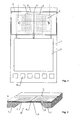
- Fig. 1 and its cross-sectional representation in Fig. 2 illustrate an exemplary embodiment of a sensor device according to the invention.
- the sensor device illustrated represents a flow sensor for measuring a flow of liquid or gas passing the sensor device.
- the sensor device is formed by a semiconductor device. Both, a measuring element 2 and an integrated circuit 3 are integrated into the semiconductor device, however, in areas distinct from each other. Contact pads 10 in form of metal pads are accessible for electrically connecting the sensor device.
- the integrated circuit 3 may include electronic components for calculating an output signal from the signals delivered by the measuring element 2, for amplifying signals, for digitizing signals, for providing reference voltages, etc..
- the semiconductor device includes a substrate 1 on which the measuring element 2 and the integrated circuit 3 are arranged.
- the substrate 1 may be any suitable substrate for depositing integrated electrical circuitry and measuring elements on.
- the integrated circuit 3 may be processed by way of standard CMOS processing technology and may include the processing of one or more of semiconducting, conducting and insulating layers.
- the measuring element 2 may be processed simultaneously with the integrated circuit 3 and may make use of the subject layers deposited on the substrate 1.
- the substrate 1 Underneath a region where the measuring element 2 is arranged, the substrate 1 provides for an opening or - as depicted in Fig 2 - a recess 4.
- Such recess 4 can be achieved by etching the substrate 1 from its back-side by means of a suitable etchant and by using the first insulating layer as an etchant stop.
- a membrane 5 is fabricated in the semiconductor device.
- the membrane 5 does not extend into the region of the integrated circuit 3. Instead, the substrate 1 fully extends underneath the region of the integrated circuit 3.
- an integrated circuit 3 or at least parts of it may be arranged in a zone close to the membrane 5 where the substrate not necessarily fully supports such zone, but may be of sufficient presence for building an integrated circuit. Such zone may be the region where the substrate slopes towards the membrane 5.
- the membrane 5 holds the measuring element 2.
- the measuring element 2 includes a heater 6 and two meandering thermopiles 7, 8 aligned symmetrically with respect to the heater 6.
- the sensor device is arranged with respect to the flow of the medium to be measured such that the medium first passes the first thermopile 7, then the heater 6 and finally the second thermopile 8.
- the thermopiles 7 and 8 are embodied as temperature sensors. By means of temperature signals provided by the thermopiles 7 and 8 a mass flow of the medium can be determined. Especially, a difference in temperature between the two thermopiles 7 and 8 is a function of the mass flow.
- the general principle of operation of measuring element 2 is described in more detail in " Scaling of Thermal CMOS Gas Flow Microsensors: Experiment and Simulation" by F. Mayer et al., in Proc. IEEE Micro Electro Mechanical Systems, (IEEE, 1996), pp. 116ff .
- the measuring element 2 is covered by a first coating 9 which is under tensile stress.
- the first coating 9 extends beyond the membrane 5 on all sides or at least on two opposite sides of the recess 4. Such overlap provides anchoring for the first coating 9 on the substrate 1 or layers deposited on the substrate 1 for receiving the tension.
- the first coating 9 is covered by a second coating 11 which is under compressive stress.
- tensile stress results from pressure forces acting within the plane of the respective coating / layer in a direction towards a coupling of the membrane 5 with the substrate 1.
- compressive stress results from forces acting within the plane of the respective layer / coating in opposite direction than tensile forces, i.e. a direction towards a centre or centreline of the membrane 5.
- the first coating 9 exhibiting tensile stress can advantageously comprise or even consist of one of silicon oxide, silicon nitride, a polymer, in particular polyimide, "Diamond Like Carbon” (DLC), polyether ether ketone (PEEK) and silicon. Silicon nitride has been found to be especially suited.
- the tensile stress in the first coating 9 can be generated and controlled by suitable choice of manufacturing parameters in known methods, see e.g. U. Münch et al., "Industrial Fabrication Technology for CMOS Infrared Sensor Arrays” in “Transducers '97, International conference on Solid State Sensors and Actuators", IEEE 1997 .
- This quotation teaches how, by suitable selection of the low frequency power and the pressure in a PECVD method, the tensile stress of a layer of oxynitride can be adjusted.
- the first coating 9 under tensile stress can also be manufactured by applying a coating material with a thermal expansion coefficient higher than silicon at an elevated temperature onto substrate 1. When cooling the sensor device down, a tensile coating is generated inevitably.
- any planar design of the coating 9 may be pre-determined such that the height - in the following also called thickness - of such coating 9 may be one of the parameters of choice for doing stress design.
- the second coating 11 exhibits compressive stress and protects the underlying measuring element 2.
- the compressive stress makes the second coating 11 become dense and prevents from pinholes occurring in the second coating by that hindering aggressive media from passing through. This means, that the second coating 11 is less porous than the first coating 9.
- the second coating 11 comprises silicon nitride or may even consist of silicon nitride.
- the second coating 11 is provided for protecting a topmost metal layer in the membrane from corrosion.
- the second coating 11 provides protection for the measuring element 2 in order to allow for a sustainable use of the sensor device in such chemically aggressive environment.
- the compressive stress in the second coating 11 can be generated and controlled by suitable choice of the manufacturing parameters in known methods, see e g. U. Münch et al., "Industrial Fabrication Technology for CMOS Infrared Sensor Arrays” in “Transducers '97, International conference on Solid State Sensors and Actuators", IEEE 1997 .
- the second coating 11 under compressive stress can also be manufactured by applying a coating material with a thermal expansion coefficient lower than silicon at an elevated temperature onto the substrate 1. When cooling the device down, a compressive coating is generated inevitably.
- any planar design of the coating 11 may be pre-determined such that the height - in the following also called thickness - of such coating 11 may be one of the parameters of choice for doing stress design.
- the coatings 9 and 11 are preferably designed such that a combined stress in the first coating 9 and the second coating 11 shows tensile stress properties in order to prevent the membrane from being bent or from buckling.
- the combined stress of the two coatings 9 and 11 may be considered as the sum of the individual stress values of the coatings 9 and 11 - i.e. the tensile stress value in the first coating 9 plus the compressive stress value in the second coating 11 - with any compressive stress value being by default a negative value.
- the combined stress of the two coatings 9 and 11 may be considered as the sum of the individual stress values multiplied by the thicknesses of the individual coatings - i.e. the tensile stress value of the first coating 9 multiplied by the thickness of the first coating 9 plus the compressive stress value of the second coating 11 multiplied by the thickness of the second coating 11 - with any compressive stress value being by default a negative value.
- both coatings 9 and 11 do not show different widths when applied to the membrane 5.
- the magnitude of the combined tensile stress to be achieved by the combined coatings 9 and 11 is subject to the processing and the materials used, and as such by the compressive stress induced into the membrane 5.
- the magnitude of the compressive stress to be provided for the second coating 11 is subject to the anticipated use of the sensor device and its exposure to aggressive substances.
- an absolute value of the compressive stress of the second coating 11 is preferably not less than 50 MPa for providing sufficient protection to the measuring element 2 and/or other components on/in the membrane 5.
- Such compressive stress value is advantageously provided in combination with a thickness of the second coating of not less than 100 nm.
- an absolute value of the stand-alone tensile stress of the first coating 9 preferably is not less than 150 MPa.
- the first coating 9, the second coating 11 and the membrane 5 all have the same thickness, advantageously a thickness not less than 100 nm.
- the combined stress of the two coatings 9 and 11 as the tensile stress value of the first coating 9 multiplied by the thickness of the first coating 9 plus the compressive stress value of the second coating 11 multiplied by the thickness of the second coating 11 advantageously is not less than a tensile stress value of the membrane 5 multiplied with the thickness of the membrane 5, and in a preferred embodiment is not less than 150 MPA.
- the membrane 5 may comprise multiple layers that are layers used for processing the integrated circuit 3. Therefore, the mechanical properties of these membrane 5 building layers cannot be chosen freely. Still, the overall tensile character of coatings 9 and 11 allow for keeping the membrane 5 taut and for controlling its flexing properties independently from the used manufacturing process while simultaneously the membrane 5 and its components are sufficiently protected.
- the coatings 9 and 11 only cover a part of the semiconductor device, namely the part that is meant to be exposed to the medium to be measured.
- the medium may get into touch with the entire top surface of the semiconductor device such that protection for the integrated circuit might be envisaged, too.
- the first coating 9 advantageously is limited to a region of the membrane 5 with at least slightly extending the membrane at at least two opposite sides for anchoring purposes.
- the second coating 11 may advantageously extend over the integrated circuit 2, too, and provide protection from environmental impacts.
- the second coating 11 may be deposited directly on the CMOS layers forming the integrated circuit 3 without the first coating 9 in between for the reason the tensile character of the first coating 9 may exert mechanical stress to the integrated circuit 3 possibly resulting in failures.
- the entire surface of the semiconductor device may be covered by the second coating 11, except for the contact pads 10.
- Using the sensor device other than as a flow detector may include its use as a pressure sensor, in which a pressure difference to be measured is applied over the membrane. It is noted that in such applications the combined coatings 9 and 11 may have impact on the sensitivity of such sensor device. The higher the combined tensile stress and the elastic modulus in coatings 9 and 11 are, the lower the sensitivity becomes. In another application, the sensor device may be used as a humidity sensor.
- a stack is built over the recess 4 formed by the membrane 5, the first coating 9, and the second coating 11.
- the membrane 5 may comprise multiple layers itself or may be formed by a single layer and a measuring element and/or components attached thereto
- the first coating 9 is provided on top of the membrane 5, either directly or by way of inserting an intermediate layer.
- the first coating 9 may serve additional purposes.
- the first coating 9 can even be an active part of the measuring element 2. Its material may offer dielectric or electric properties which vary depending on a parameter to be measured.
- the dielectric constant or the conductivity of a polymeric tensile coating 9 may vary depending on current humidity.
- a tensile coating 9 - provided the coating 9 is exposed to the substance to be measured - may undergo chemical reactions with such substance, or its chemical potential or work function may change. Also optical properties of the tensile coating 9 may be subject to a parameter to be measured.
- the second, protective coating 11 under compressive stress is provided on top of the first coating 9.
- such coating 11 is applied to the semiconductor device in a last step and may cover the same completely, again with the exception of the contact pads 10.
- the second coating 11 may also protect the structures of the integrated circuit 3.
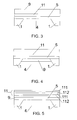
- Fig. 3 illustrates a sectional view of a stack of a sensor device according to an embodiment of the present invention.
- the stack comprises the membrane 5, the second coating 11 and the first coating 9.
- the second coating 11 is directly arranged on top of the membrane 5 while the first coating 9 is arranged on top of the second coating 11.
- the first, tensile coating 9 is the topmost layer and is exposed to the medium. Coating 9 nevertheless can provide its tensile character to the overall stack thereby causing the combined coatings 9 and 11 to counteract any compressive forces in the membrane 5.
- coating 9 may support insulating properties of second coating 11 even if coating 9 as such may not provide sufficient protection to membrane 5.
- both coatings 9 and 11 consisting of silicon nitride.
- Silicon nitride may provide excellent properties in both its tensile and compressive status in view of protection and counteracting compressive forces in the membrane 5.
- a preferred thickness of the second coating is not less than 100 nm.
- a preferred thickness of the first coating is not less than 100 nm.
- Figure 4 illustrates a sectional view of a stack of a sensor device according to another embodiment of the present invention.
- the first coating 9 now is arranged underneath the membrane 5 which back-side of the membrane 5 again is not exposed to a potentially aggressive medium.
- the first coating 9 can counteract any compressive forces induced into the membrane 5.
- the first coating 9 may even be arranged as a layer within the membrane 5 provided the membrane 5 is embodied as a multi-layer membrane 5.
- Figure 5 shows another embodiment of a stack of a sensor device according to an embodiment of the present invention.
- This stack resembles the stack of Fig. 1 and 2 in that the second coating 11 is arranged on top of the first coating 9.
- the second coating 11 itself encompasses a layer stack comprising layers of silicon nitride 111 and silicon oxide 112 in alternating order.
- Such layered structure of coating 11 provides advantages in that any pinhole or other defect in one of the layers may be covered by the next layer on top for the reason that it is not very likely that the next layer shows a pinhole or other defect at the same location.
- a propagation of pinholes from one layer into the next is not very likely either as silicon oxide and silicon nitride grow independently from each other. Consequently, the more layers are provided within the second coating 11 the better the protection is against pinholes.
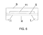
- Figure 6 shows another embodiment of a stack of a sensor device according to an embodiment of the present invention.
- This stack again resembles the stack of Fig. 1 , however, the first coating 9 does not fully cover the breadth of the device but only overlaps the breadth of the membrane slightly for anchoring purposes.
- the second coating 11 extends to the full breadth of the device, and is directly deposited on the CMOS layers where the first coating 9 does not extend very much beyond the membrane 5.
- any region where an integrated circuit is arranged in the semiconductor device Such region is free from the first coating 9, however, advantageously covered by the second coating 11 in order to provide protection.
- the sensor device may comprise an enclosure designed for holding a fluid such as a liquid or a gas.
- the measuring element may be arranged such that it is exposed to the fluid to be measured.
- the enclosure may take the form of a housing, or of a duct.
- the membrane including the measuring element may be integrated in a wall of such enclosure.
- the fluid to be measured advantageously is ammonia
- the parameter of the fluid to be measured advantageously is the mass flow of ammonia
Landscapes
- Physics & Mathematics (AREA)
- Fluid Mechanics (AREA)
- General Physics & Mathematics (AREA)
- Pressure Sensors (AREA)
Abstract
Semiconductor sensor device with a membrane (5) to be operated in a chemically aggressive environment. While the sensor device provides for a first coating (9) under tensile stress, that compensates for e.g. thermally induced compressive stress in the membrane (5) as a result of manufacturing, a second coating (11) is meant to protect the membrane (5) against the environment. For such protection, the second coating (11) is under compressive stress, however, the combined stress of first and second coating (9,11) is of tensile character such that any compressive stress in the membrane (5) still can be compensated. Preferably, both coatings (9,11) comprise silicon nitride.
Description
- The present invention relates to a sensor device, its use, and a method for its manufacture.
- The trend of miniaturization and integration not only affects electronic circuits but also sensors. While conventional sensors were often built from discrete components and connected to electric circuits by means of leads new sensor devices are built on substrates which substrates most often carry electronic circuits embodied by semiconducting structures built on such a common substrate.
- Sensor devices can be embodied for measuring flow, temperature, pressure, or other measures. Measuring elements for such sensor devices may be thermo-couplers or the like. A preferred location for arranging measuring elements in such sensor devices is on a membrane. The rationale for arranging a measuring element on a membrane may be one or more of the membrane being part of the measuring system, e.g. the membrane being deflected and allowing for measuring pressure, the membrane being accessible from the backside for processing purposes, or the membrane being advantageously decoupled from the substrate for improving measurement results.
- As long as the sensor device provides an associate integrated circuit, a membrane of the sensor device most often is formed by layers of one or more of semiconducting, insulating and conductive material which layers are deposited for building the integrated circuit. The membrane can be regarded as sort of a by-product as it can be processed simply by removing the substrate in the subject area.
- However, during the manufacturing process the layers and the substrate may be heated and cooled down to different temperatures and consequently may show different temperature induced behaviour during such processing steps. A typical problem addressed in
PCT Application WO 02/055967 A1 WO 02/055967 A1 - While the above International Application does raise the need for an additional protective layer embodied as a silicon nitride layer for protecting electronic components of the integrated circuit, it explicitly discourages from covering the membrane with such protective layer due to the compressive properties of such protective layer which otherwise would re-compensate for the effects evoked by the tensile coating. Consequently, provision of such silicon nitride layer as protective means is restricted to areas outside the membrane. On the other hand, the protective effect of the tensile coating may not be sufficient subject to the medium protection should be sought from.
- The problem to be solved by the present invention is therefore to provide a sensor device which improves protection of the membrane against damaging impact. Such impact may result from the medium to be measured itself if, for instance, such medium exhibits chemically aggressive properties as ammonia does.
- This problem is solved by a sensor device according to the features of
independent claim 1. - In addition to the first coating under tensile stress, the sensor device comprises a second coating under compressive stress. The second coating comprises silicon nitride. The first and the second coatings are designed such that a combined stress of the first and the second coating is of tensile nature in order to compensate for compressive stress induced into the membrane.
- The resulting sensor device not only compensates for compressive stress induced into the membrane, but also protects the membrane and components arranged on or in the membrane against chemically aggressive environments. The protective property is owed to the compressive nature of the second coating which leads to a high density in such coating. The high density, in turn, prevents from pinholes in the coating by that making the second coating less porous for damaging media such that underlying structures are protected. In case of an arrangement of the compressive coating on top of the tensile coating the tensile coating may have pinholes owed to its tensile nature for the reason that the compressive coating provides protection.
- In a preferred embodiment, the second coating extends over at least a part of or even the entirety of an integrated circuit arranged in a semiconductor device. Hence, a single second coating may protect the membrane and such integrated circuit from an aggressive environment in cases where the membrane and an integrated circuit are integrated in a common semiconductor device.
- For other advantageous embodiments it is referred to the dependent claims. Many of the embodiments relate to the design of a stack of coatings and membrane, or to the compressive / tensile properties of the respective coatings.
- A number of embodiments of the present invention will now be described by way of example only and with reference to the accompanying drawings, in which the figures show:
-
Fig. 1 a top view of a sensor device according to an embodiment of the present invention, -
Fig. 2 a cross-sectional view of the sensor device according toFigure 1 along the lines II-II, -
Fig. 3 a cross-sectional view of a stack of a sensor device according to an embodiment of the present invention, -
Fig. 4 a cross-sectional view of another stack of a sensor device according to an embodiment of the present invention, -
Fig. 5 a cross-sectional view of another stack of a sensor device according to an embodiment of the present invention, and -
Fig. 6 a cross-sectional view of another stack of a sensor device according to an embodiment of the present invention. -
Fig. 1 and its cross-sectional representation inFig. 2 illustrate an exemplary embodiment of a sensor device according to the invention. The sensor device illustrated represents a flow sensor for measuring a flow of liquid or gas passing the sensor device. - The sensor device is formed by a semiconductor device. Both, a measuring element 2 and an integrated circuit 3 are integrated into the semiconductor device, however, in areas distinct from each other. Contact
pads 10 in form of metal pads are accessible for electrically connecting the sensor device. - The integrated circuit 3 may include electronic components for calculating an output signal from the signals delivered by the measuring element 2, for amplifying signals, for digitizing signals, for providing reference voltages, etc..
- The semiconductor device includes a
substrate 1 on which the measuring element 2 and the integrated circuit 3 are arranged. Thesubstrate 1 may be any suitable substrate for depositing integrated electrical circuitry and measuring elements on. - The integrated circuit 3 may be processed by way of standard CMOS processing technology and may include the processing of one or more of semiconducting, conducting and insulating layers. The measuring element 2 may be processed simultaneously with the integrated circuit 3 and may make use of the subject layers deposited on the
substrate 1. - Underneath a region where the measuring element 2 is arranged, the
substrate 1 provides for an opening or - as depicted inFig 2 - arecess 4.Such recess 4 can be achieved by etching thesubstrate 1 from its back-side by means of a suitable etchant and by using the first insulating layer as an etchant stop. - By etching the recess 4 a
membrane 5 is fabricated in the semiconductor device. Note that in the present embodiment themembrane 5 does not extend into the region of the integrated circuit 3. Instead, thesubstrate 1 fully extends underneath the region of the integrated circuit 3. However, in other embodiments an integrated circuit 3 or at least parts of it may be arranged in a zone close to themembrane 5 where the substrate not necessarily fully supports such zone, but may be of sufficient presence for building an integrated circuit. Such zone may be the region where the substrate slopes towards themembrane 5. - The
membrane 5 holds the measuring element 2. The measuring element 2 includes a heater 6 and two meanderingthermopiles first thermopile 7, then the heater 6 and finally thesecond thermopile 8. Thethermopiles thermopiles 7 and 8 a mass flow of the medium can be determined. Especially, a difference in temperature between the twothermopiles - In the present embodiment, the measuring element 2 is covered by a
first coating 9 which is under tensile stress. Thefirst coating 9 extends beyond themembrane 5 on all sides or at least on two opposite sides of therecess 4. Such overlap provides anchoring for thefirst coating 9 on thesubstrate 1 or layers deposited on thesubstrate 1 for receiving the tension. - The
first coating 9 is covered by asecond coating 11 which is under compressive stress. - Throughout the present patent application it is understood that tensile stress results from pressure forces acting within the plane of the respective coating / layer in a direction towards a coupling of the
membrane 5 with thesubstrate 1. In turn, compressive stress results from forces acting within the plane of the respective layer / coating in opposite direction than tensile forces, i.e. a direction towards a centre or centreline of themembrane 5. - The
first coating 9 exhibiting tensile stress can advantageously comprise or even consist of one of silicon oxide, silicon nitride, a polymer, in particular polyimide, "Diamond Like Carbon" (DLC), polyether ether ketone (PEEK) and silicon. Silicon nitride has been found to be especially suited. - The tensile stress in the
first coating 9 can be generated and controlled by suitable choice of manufacturing parameters in known methods, see e.g. U. Münch et al., "Industrial Fabrication Technology for CMOS Infrared Sensor Arrays" in "Transducers '97, International conference on Solid State Sensors and Actuators", IEEE 1997. This quotation teaches how, by suitable selection of the low frequency power and the pressure in a PECVD method, the tensile stress of a layer of oxynitride can be adjusted. - The
first coating 9 under tensile stress can also be manufactured by applying a coating material with a thermal expansion coefficient higher than silicon at an elevated temperature ontosubstrate 1. When cooling the sensor device down, a tensile coating is generated inevitably. - As stress is defined by force per area, the dimensioning of the cross-section of the
coating 9 is critical to determine the stress in thecoating 9. In most embodiments, any planar design of thecoating 9 may be pre-determined such that the height - in the following also called thickness - ofsuch coating 9 may be one of the parameters of choice for doing stress design. - The
second coating 11 exhibits compressive stress and protects the underlying measuring element 2. The compressive stress makes thesecond coating 11 become dense and prevents from pinholes occurring in the second coating by that hindering aggressive media from passing through. This means, that thesecond coating 11 is less porous than thefirst coating 9. Thesecond coating 11 comprises silicon nitride or may even consist of silicon nitride. - The
second coating 11 is provided for protecting a topmost metal layer in the membrane from corrosion. When operating the sensor device in an ammonia environment, for instance, thesecond coating 11 provides protection for the measuring element 2 in order to allow for a sustainable use of the sensor device in such chemically aggressive environment. - The compressive stress in the
second coating 11 can be generated and controlled by suitable choice of the manufacturing parameters in known methods, see e g. U. Münch et al., "Industrial Fabrication Technology for CMOS Infrared Sensor Arrays" in "Transducers '97, International conference on Solid State Sensors and Actuators", IEEE 1997. - The
second coating 11 under compressive stress can also be manufactured by applying a coating material with a thermal expansion coefficient lower than silicon at an elevated temperature onto thesubstrate 1. When cooling the device down, a compressive coating is generated inevitably. - As stress is defined by force per area, the dimensioning of the cross-section of the
coating 11 is critical to determine the stress in thecoating 11. In most embodiments, any planar design of thecoating 11 may be pre-determined such that the height - in the following also called thickness - ofsuch coating 11 may be one of the parameters of choice for doing stress design. - Focus now is turned to the dimensioning of
coatings coatings first coating 9 and thesecond coating 11 shows tensile stress properties in order to prevent the membrane from being bent or from buckling. Provided the twocoatings coatings coatings 9 and 11 - i.e. the tensile stress value in thefirst coating 9 plus the compressive stress value in the second coating 11 - with any compressive stress value being by default a negative value. If the twocoatings coatings first coating 9 multiplied by the thickness of thefirst coating 9 plus the compressive stress value of thesecond coating 11 multiplied by the thickness of the second coating 11 - with any compressive stress value being by default a negative value. - In case the
coatings coatings membrane 5. - The magnitude of the combined tensile stress to be achieved by the combined
coatings membrane 5. On the other hand, the magnitude of the compressive stress to be provided for thesecond coating 11 is subject to the anticipated use of the sensor device and its exposure to aggressive substances. - For its use in an ammonia environment, for example, an absolute value of the compressive stress of the
second coating 11 is preferably not less than 50 MPa for providing sufficient protection to the measuring element 2 and/or other components on/in the membrane 5.Such compressive stress value is advantageously provided in combination with a thickness of the second coating of not less than 100 nm. - Under the assumption that a preferred absolute value of the combined tensile stress of the first and
second coating membrane 5 induced bysubstrate 1 during processing, an absolute value of the stand-alone tensile stress of thefirst coating 9 preferably is not less than 150 MPa. Advantageously, thefirst coating 9, thesecond coating 11 and themembrane 5 all have the same thickness, advantageously a thickness not less than 100 nm. - If the thickness of at least one of the
coatings membrane 5 is different to the thickness of the other layers, the combined stress of the twocoatings first coating 9 multiplied by the thickness of thefirst coating 9 plus the compressive stress value of thesecond coating 11 multiplied by the thickness of thesecond coating 11 advantageously is not less than a tensile stress value of themembrane 5 multiplied with the thickness of themembrane 5, and in a preferred embodiment is not less than 150 MPA. - The
membrane 5 may comprise multiple layers that are layers used for processing the integrated circuit 3. Therefore, the mechanical properties of thesemembrane 5 building layers cannot be chosen freely. Still, the overall tensile character ofcoatings membrane 5 taut and for controlling its flexing properties independently from the used manufacturing process while simultaneously themembrane 5 and its components are sufficiently protected. - In
Fig. 1 and 2 , thecoatings first coating 9 advantageously is limited to a region of themembrane 5 with at least slightly extending the membrane at at least two opposite sides for anchoring purposes. Thesecond coating 11 may advantageously extend over the integrated circuit 2, too, and provide protection from environmental impacts. In the region of the integrated circuit 3, thesecond coating 11 may be deposited directly on the CMOS layers forming the integrated circuit 3 without thefirst coating 9 in between for the reason the tensile character of thefirst coating 9 may exert mechanical stress to the integrated circuit 3 possibly resulting in failures. Advantageously, the entire surface of the semiconductor device may be covered by thesecond coating 11, except for thecontact pads 10. - Using the sensor device other than as a flow detector may include its use as a pressure sensor, in which a pressure difference to be measured is applied over the membrane. It is noted that in such applications the combined
coatings coatings - In the embodiment according to
Fig. 1 and 2 , a stack is built over therecess 4 formed by themembrane 5, thefirst coating 9, and thesecond coating 11. While themembrane 5 may comprise multiple layers itself or may be formed by a single layer and a measuring element and/or components attached thereto, thefirst coating 9 is provided on top of themembrane 5, either directly or by way of inserting an intermediate layer. In a set-up where thefirst coating 9 is arranged on top or underneath themembrane 5 thefirst coating 9 may serve additional purposes. For example, thefirst coating 9 can even be an active part of the measuring element 2. Its material may offer dielectric or electric properties which vary depending on a parameter to be measured. In a humidity sensor, for example, the dielectric constant or the conductivity of a polymerictensile coating 9 may vary depending on current humidity. In a substance detector, for example, a tensile coating 9 - provided thecoating 9 is exposed to the substance to be measured - may undergo chemical reactions with such substance, or its chemical potential or work function may change. Also optical properties of thetensile coating 9 may be subject to a parameter to be measured. - In the arrangement of
Fig. 1 and 2 , the second,protective coating 11 under compressive stress is provided on top of thefirst coating 9. In a standard CMOS manufacturing processsuch coating 11 is applied to the semiconductor device in a last step and may cover the same completely, again with the exception of thecontact pads 10. Thus, thesecond coating 11 may also protect the structures of the integrated circuit 3. -
Fig. 3 illustrates a sectional view of a stack of a sensor device according to an embodiment of the present invention. The stack comprises themembrane 5, thesecond coating 11 and thefirst coating 9. In this embodiment, thesecond coating 11 is directly arranged on top of themembrane 5 while thefirst coating 9 is arranged on top of thesecond coating 11. It is assumed that the medium to be measured only approaches the top of the stack while the free back-side of themembrane 5 is not exposed to any damaging medium. In this embodiment, the first,tensile coating 9 is the topmost layer and is exposed to the medium.Coating 9 nevertheless can provide its tensile character to the overall stack thereby causing the combinedcoatings membrane 5. Additionally,coating 9 may support insulating properties ofsecond coating 11 even if coating 9 as such may not provide sufficient protection tomembrane 5. - In the present embodiment, as well as in any other embodiment, it is advantageous to have both
coatings membrane 5. - Irrespective of the present embodiment, a preferred thickness of the second coating is not less than 100 nm. Again, irrespective of the present embodiment a preferred thickness of the first coating is not less than 100 nm.
-
Figure 4 illustrates a sectional view of a stack of a sensor device according to another embodiment of the present invention. In contrast to the stack inFig. 3 , thefirst coating 9 now is arranged underneath themembrane 5 which back-side of themembrane 5 again is not exposed to a potentially aggressive medium. In such embodiment, thefirst coating 9 can counteract any compressive forces induced into themembrane 5. In yet another embodiment, thefirst coating 9 may even be arranged as a layer within themembrane 5 provided themembrane 5 is embodied as amulti-layer membrane 5. -
Figure 5 shows another embodiment of a stack of a sensor device according to an embodiment of the present invention. This stack resembles the stack ofFig. 1 and 2 in that thesecond coating 11 is arranged on top of thefirst coating 9. However, thesecond coating 11 itself encompasses a layer stack comprising layers ofsilicon nitride 111 andsilicon oxide 112 in alternating order. Such layered structure ofcoating 11 provides advantages in that any pinhole or other defect in one of the layers may be covered by the next layer on top for the reason that it is not very likely that the next layer shows a pinhole or other defect at the same location. A propagation of pinholes from one layer into the next is not very likely either as silicon oxide and silicon nitride grow independently from each other. Consequently, the more layers are provided within thesecond coating 11 the better the protection is against pinholes. -
Figure 6 shows another embodiment of a stack of a sensor device according to an embodiment of the present invention. This stack again resembles the stack ofFig. 1 , however, thefirst coating 9 does not fully cover the breadth of the device but only overlaps the breadth of the membrane slightly for anchoring purposes. Still, thesecond coating 11 extends to the full breadth of the device, and is directly deposited on the CMOS layers where thefirst coating 9 does not extend very much beyond themembrane 5. The same holds for any region where an integrated circuit is arranged in the semiconductor device: Such region is free from thefirst coating 9, however, advantageously covered by thesecond coating 11 in order to provide protection. - The sensor device may comprise an enclosure designed for holding a fluid such as a liquid or a gas.
The measuring element may be arranged such that it is exposed to the fluid to be measured. The enclosure may take the form of a housing, or of a duct. The membrane including the measuring element may be integrated in a wall of such enclosure. - The fluid to be measured advantageously is ammonia, and the parameter of the fluid to be measured advantageously is the mass flow of ammonia.
-
- 1
- Substrate
- 2
- Measuring element
- 3
- Integrated circuit
- 4
- Recess
- 5
- Membrane
- 6
- Heater
- 7
- First thermopile
- 8
- Second thermopile
- 9
- First coating
- 10
- Contact pad
- 11
- Second coating
- 111
- Silicon nitride layer
- 112
- Silicon oxide layer
Claims (15)
- Sensor device, comprising- a membrane (5) with a measuring element (2),- a first coating (9) under tensile stress, and- a second coating (11),
characterized in that the second coating (11) is under compressive stress and comprises silicon nitride, and that a combined stress of the first and the second coating (9, 11) is of tensile nature. - Sensor device of claim 1, wherein the second coating (11) comprises a layer stack, a first layer (111) of which layer stack comprising silicon nitride and a second layer (112) comprising silicon oxide.
- Sensor device of claim 2, wherein the layer stack comprises multiple layers (111, 112) of silicon nitride and silicon oxide in alternating order.
- Sensor device of one of the preceding claims, wherein the first coating (9) comprises silicon nitride.
- Sensor device of one of the preceding claims, wherein the membrane (5), the first coating (9) and the second coating (11) are arranged in a stack.
- Sensor device of claim 6, wherein the first coating (9) is arranged between the membrane (5) and the second coating (11).
- Sensor device of claim 5, wherein the second coating (11) is arranged between the membrane (5) and the first coating (9).
- Sensor device of one of the preceding claims, wherein a thickness of the second coating (11) is not less than 100nm.
- Sensor device of one of the preceding claims, wherein an absolute value of the compressive stress of the second coating (11) is not less than 50 MPa.
- Sensor device of one of the preceding claims, wherein an absolute value of the tensile stress of the first coating (9) is not less than 100 MPa.
- Sensor device of one of the preceding claims, wherein an absolute value of the combined stress is not less than 100 MPa.
- Sensor device of one of the preceding claims, comprising a semiconductor device including an integrated circuit (3), wherein the second coating (11) covers at least a part of the integrated circuit (3).
- Sensor device of claim 12, wherein the first coating (9) does not extend over the integrated circuit (3).
- Sensor device of one of the preceding claims, comprising an enclosure designed for holding ammonia, wherein the measuring element (2) being arranged for measuring an ammonia related parameter.
- Use of a sensor device of one of the preceding claims as a flow sensor for measuring the flow of ammonia.
Priority Applications (1)
| Application Number | Priority Date | Filing Date | Title |
|---|---|---|---|
| EP10000239A EP2348292A1 (en) | 2010-01-13 | 2010-01-13 | Sensor device |
Applications Claiming Priority (1)
| Application Number | Priority Date | Filing Date | Title |
|---|---|---|---|
| EP10000239A EP2348292A1 (en) | 2010-01-13 | 2010-01-13 | Sensor device |
Publications (1)
| Publication Number | Publication Date |
|---|---|
| EP2348292A1 true EP2348292A1 (en) | 2011-07-27 |
Family
ID=42334021
Family Applications (1)
| Application Number | Title | Priority Date | Filing Date |
|---|---|---|---|
| EP10000239A Withdrawn EP2348292A1 (en) | 2010-01-13 | 2010-01-13 | Sensor device |
Country Status (1)
| Country | Link |
|---|---|
| EP (1) | EP2348292A1 (en) |
Cited By (10)
| Publication number | Priority date | Publication date | Assignee | Title |
|---|---|---|---|---|
| WO2014102086A1 (en) * | 2012-12-21 | 2014-07-03 | Innovative Sensor Technology Ist Ag | Sensor for determining a process variable of a medium |
| EP2762864A1 (en) * | 2013-01-31 | 2014-08-06 | Sensirion AG | Membrane-based sensor device and method for manufacturing the same |
| WO2015182257A1 (en) * | 2014-05-28 | 2015-12-03 | 日立オートモティブシステムズ株式会社 | Flow rate sensor and method for manufacturing same |
| WO2016111096A1 (en) * | 2015-01-09 | 2016-07-14 | 日立オートモティブシステムズ株式会社 | Thermal fluid flow-rate sensor |
| US9506885B2 (en) | 2014-09-26 | 2016-11-29 | Sensirion Ag | Sensor chip |
| US9612146B2 (en) | 2014-02-07 | 2017-04-04 | Honeywell International, Inc. | Airflow sensor with dust reduction |
| WO2019135004A1 (en) * | 2018-01-05 | 2019-07-11 | Hahn-Schickard-Gesellschaft für angewandte Forschung e.V. | Gas sensor, and method for operating the gas sensor |
| WO2019215981A1 (en) * | 2018-05-08 | 2019-11-14 | 日立オートモティブシステムズ株式会社 | Thermal-type sensor device |
| WO2020116016A1 (en) * | 2018-12-05 | 2020-06-11 | 日立オートモティブシステムズ株式会社 | Thermal sensor and method for manufacturing same, and semiconductor device |
| EP3735580B1 (en) * | 2018-01-05 | 2022-04-27 | Hahn-Schickard-Gesellschaft für angewandte Forschung e.V. | Evaluation arrangement for a thermal gas sensor, method and computer program product |
Citations (6)
| Publication number | Priority date | Publication date | Assignee | Title |
|---|---|---|---|---|
| WO2002055967A1 (en) | 2001-01-10 | 2002-07-18 | Sensirion Ag | Micromechanical flow sensor with a tensile coating |
| US20030019290A1 (en) * | 2001-07-27 | 2003-01-30 | Takao Iwaki | Flow sensor |
| US20040147057A1 (en) * | 2001-04-07 | 2004-07-29 | Hubert Benzel | Method for producing a semiconductor component and a semiconductor component produced according to this method |
| US20060160314A1 (en) * | 2005-01-15 | 2006-07-20 | Applied Materials, Inc. | Substrate having silicon germanium material and stressed silicon nitride layer |
| EP1944585A2 (en) * | 2007-01-15 | 2008-07-16 | Hitachi, Ltd. | Thermal type fluid sensor and manufacturing method thereof |
| EP2085754A2 (en) * | 2008-01-29 | 2009-08-05 | Hitachi Ltd. | Flow sensor with metal film resistor |
-
2010
- 2010-01-13 EP EP10000239A patent/EP2348292A1/en not_active Withdrawn
Patent Citations (6)
| Publication number | Priority date | Publication date | Assignee | Title |
|---|---|---|---|---|
| WO2002055967A1 (en) | 2001-01-10 | 2002-07-18 | Sensirion Ag | Micromechanical flow sensor with a tensile coating |
| US20040147057A1 (en) * | 2001-04-07 | 2004-07-29 | Hubert Benzel | Method for producing a semiconductor component and a semiconductor component produced according to this method |
| US20030019290A1 (en) * | 2001-07-27 | 2003-01-30 | Takao Iwaki | Flow sensor |
| US20060160314A1 (en) * | 2005-01-15 | 2006-07-20 | Applied Materials, Inc. | Substrate having silicon germanium material and stressed silicon nitride layer |
| EP1944585A2 (en) * | 2007-01-15 | 2008-07-16 | Hitachi, Ltd. | Thermal type fluid sensor and manufacturing method thereof |
| EP2085754A2 (en) * | 2008-01-29 | 2009-08-05 | Hitachi Ltd. | Flow sensor with metal film resistor |
Non-Patent Citations (2)
| Title |
|---|
| F. MAYER ET AL.: "Scaling of Thermal CMOS Gas Flow Microsensors: Experiment and Simulation", PROC. IEEE MICRO ELECTRO MECHANICAL SYSTEMS, 1996, pages 116FF |
| U. MUNCH ET AL.: "Industrial Fabrication Technology for CMOS Infrared Sensor Arrays", TRANSDUCERS '97, INTERNATIONAL CONFERENCE ON SOLID STATE SENSORS AND ACTUATORS, 1997 |
Cited By (22)
| Publication number | Priority date | Publication date | Assignee | Title |
|---|---|---|---|---|
| US10345129B2 (en) | 2012-12-21 | 2019-07-09 | Innovative Sensor Technology Ist Ag | Sensor with metal substrate and dielectric membrane for determining a process variable of a medium |
| WO2014102086A1 (en) * | 2012-12-21 | 2014-07-03 | Innovative Sensor Technology Ist Ag | Sensor for determining a process variable of a medium |
| EP2762864A1 (en) * | 2013-01-31 | 2014-08-06 | Sensirion AG | Membrane-based sensor device and method for manufacturing the same |
| US9224658B2 (en) | 2013-01-31 | 2015-12-29 | Sensirion Ag | Membrane-based sensor device with non-dielectric etch-stop layer around substrate recess |
| US9612146B2 (en) | 2014-02-07 | 2017-04-04 | Honeywell International, Inc. | Airflow sensor with dust reduction |
| WO2015182257A1 (en) * | 2014-05-28 | 2015-12-03 | 日立オートモティブシステムズ株式会社 | Flow rate sensor and method for manufacturing same |
| JP2015224993A (en) * | 2014-05-28 | 2015-12-14 | 日立オートモティブシステムズ株式会社 | Flow sensor and manufacturing method thereof |
| US9506885B2 (en) | 2014-09-26 | 2016-11-29 | Sensirion Ag | Sensor chip |
| US10393557B2 (en) | 2015-01-09 | 2019-08-27 | Hitachi Automotive Systems, Ltd. | Thermal fluid flow sensor |
| WO2016111096A1 (en) * | 2015-01-09 | 2016-07-14 | 日立オートモティブシステムズ株式会社 | Thermal fluid flow-rate sensor |
| JP2016128770A (en) * | 2015-01-09 | 2016-07-14 | 日立オートモティブシステムズ株式会社 | Thermal fluid flow sensor |
| WO2019135004A1 (en) * | 2018-01-05 | 2019-07-11 | Hahn-Schickard-Gesellschaft für angewandte Forschung e.V. | Gas sensor, and method for operating the gas sensor |
| KR20200101989A (en) * | 2018-01-05 | 2020-08-28 | 한-식카드-게셀쉐프트 퓨어 안게반테 포슝 이.브이. | Gas sensor and method for operating the gas sensor |
| EP3735580B1 (en) * | 2018-01-05 | 2022-04-27 | Hahn-Schickard-Gesellschaft für angewandte Forschung e.V. | Evaluation arrangement for a thermal gas sensor, method and computer program product |
| US11454622B2 (en) | 2018-01-05 | 2022-09-27 | Hahn-Schickard-Gesellschaft für angewandte Forschung e.V. | Gas sensor, and method for operating the gas sensor |
| US11686695B2 (en) | 2018-01-05 | 2023-06-27 | Hahn-Schickard-Gesellschaft für angewandte Forschung e.V. | Evaluation arrangement for a thermal gas sensor, methods and computer programs |
| US11874242B2 (en) | 2018-01-05 | 2024-01-16 | Habn-Schickard-Gesellschaft für angewandte Forschung e.V. | Evaluation arrangement for a thermal gas sensor, methods and computer programs |
| US12385862B2 (en) | 2018-01-05 | 2025-08-12 | Hahn-Schickard-Gesellschaft für angewandte Forschung e.V. | Evaluation arrangement for a thermal gas sensor, methods and computer programs |
| WO2019215981A1 (en) * | 2018-05-08 | 2019-11-14 | 日立オートモティブシステムズ株式会社 | Thermal-type sensor device |
| WO2020116016A1 (en) * | 2018-12-05 | 2020-06-11 | 日立オートモティブシステムズ株式会社 | Thermal sensor and method for manufacturing same, and semiconductor device |
| JP2020091191A (en) * | 2018-12-05 | 2020-06-11 | 日立オートモティブシステムズ株式会社 | Thermal sensor, manufacturing method thereof, and semiconductor device |
| JP6990165B2 (en) | 2018-12-05 | 2022-01-12 | 日立Astemo株式会社 | Thermal sensors and their manufacturing methods and semiconductor devices |
Similar Documents
| Publication | Publication Date | Title |
|---|---|---|
| US7154372B2 (en) | Micromechanical flow sensor with tensile coating | |
| US6184773B1 (en) | Rugged fluid flow and property microsensor | |
| US8130072B2 (en) | Vanadium oxide thermal microprobes | |
| EP2762864B1 (en) | Membrane-based sensor device and method for manufacturing the same | |
| Marsi et al. | Development of high temperature resistant of 500° C employing silicon carbide (3C-SiC) based MEMS pressure sensor | |
| KR102696081B1 (en) | Microelectromechanical system | |
| TWI648527B (en) | Improved pressure sensor structure | |
| EP2762866B1 (en) | CMOS gas sensor and method for manufacturing the same | |
| US7051595B2 (en) | Monolithic multi-functional integrated sensor and method for fabricating the same | |
| Sheeparamatti et al. | Fabrication and characterization of polysilicon-on-insulator (PolySOI) and a-SOI based micro piezoresistive pressure sensor for harsh environment applications | |
| WO2009096504A1 (en) | Micro vacuum gauge | |
| US8399811B2 (en) | Stage for substrate temperature control apparatus | |
| Zhang et al. | Characterization of a silicon nanowire-based cantilever air-flow sensor | |
| JP7049747B2 (en) | Gas sensor, content component detection device equipped with gas sensor, inspection system equipped with gas sensor, inspection method of gas sensor, manufacturing method of gas sensor | |
| Marsi et al. | RETRACTED ARTICLE: A MEMS packaged capacitive pressure sensor employing 3C-SiC with operating temperature of 500° C | |
| EP3301072B1 (en) | Semiconductor device and method for forming a semiconductor device | |
| CN114746733A (en) | Pressure measuring sensor | |
| US7185539B2 (en) | Flow sensor | |
| Iwata et al. | Design, fabrication, and characterization of bridge-type micro-hotplates with an SU-8 supporting layer for a smart gas sensing system | |
| WO2006020674A1 (en) | Silicon carbide mems structures and methods of forming the same | |
| Lee et al. | A concave-patterned TiN/PECVD-Si3N4/TiN diaphragm MEMS acoustic sensor based on a polyimide sacrificial layer | |
| KR20100110213A (en) | Micro heat flux sensor and method for producing the said sensor | |
| EP2938570B1 (en) | Surface charge mitigation layer for mems sensors | |
| Demirci et al. | Electro-thermal simulations and modelling of micromachined gas sensor | |
| JP6990165B2 (en) | Thermal sensors and their manufacturing methods and semiconductor devices |
Legal Events
| Date | Code | Title | Description |
|---|---|---|---|
| PUAI | Public reference made under article 153(3) epc to a published international application that has entered the european phase |
Free format text: ORIGINAL CODE: 0009012 |
|
| AK | Designated contracting states |
Kind code of ref document: A1 Designated state(s): AT BE BG CH CY CZ DE DK EE ES FI FR GB GR HR HU IE IS IT LI LT LU LV MC MK MT NL NO PL PT RO SE SI SK SM TR |
|
| AX | Request for extension of the european patent |
Extension state: AL BA RS |
|
| STAA | Information on the status of an ep patent application or granted ep patent |
Free format text: STATUS: THE APPLICATION IS DEEMED TO BE WITHDRAWN |
|
| 18D | Application deemed to be withdrawn |
Effective date: 20120128 |