EP2346669B1 - Improvements for rapid prototyping apparatus - Google Patents
Improvements for rapid prototyping apparatus Download PDFInfo
- Publication number
- EP2346669B1 EP2346669B1 EP09783883.3A EP09783883A EP2346669B1 EP 2346669 B1 EP2346669 B1 EP 2346669B1 EP 09783883 A EP09783883 A EP 09783883A EP 2346669 B1 EP2346669 B1 EP 2346669B1
- Authority
- EP
- European Patent Office
- Prior art keywords
- light
- emitting diode
- circuit board
- printed circuit
- light emitting
- Prior art date
- Legal status (The legal status is an assumption and is not a legal conclusion. Google has not performed a legal analysis and makes no representation as to the accuracy of the status listed.)
- Active
Links
Images







Classifications
-
- B—PERFORMING OPERATIONS; TRANSPORTING
- B29—WORKING OF PLASTICS; WORKING OF SUBSTANCES IN A PLASTIC STATE IN GENERAL
- B29C—SHAPING OR JOINING OF PLASTICS; SHAPING OF MATERIAL IN A PLASTIC STATE, NOT OTHERWISE PROVIDED FOR; AFTER-TREATMENT OF THE SHAPED PRODUCTS, e.g. REPAIRING
- B29C67/00—Shaping techniques not covered by groups B29C39/00 - B29C65/00, B29C70/00 or B29C73/00
-
- B—PERFORMING OPERATIONS; TRANSPORTING
- B29—WORKING OF PLASTICS; WORKING OF SUBSTANCES IN A PLASTIC STATE IN GENERAL
- B29C—SHAPING OR JOINING OF PLASTICS; SHAPING OF MATERIAL IN A PLASTIC STATE, NOT OTHERWISE PROVIDED FOR; AFTER-TREATMENT OF THE SHAPED PRODUCTS, e.g. REPAIRING
- B29C64/00—Additive manufacturing, i.e. manufacturing of three-dimensional [3D] objects by additive deposition, additive agglomeration or additive layering, e.g. by 3D printing, stereolithography or selective laser sintering
- B29C64/10—Processes of additive manufacturing
- B29C64/106—Processes of additive manufacturing using only liquids or viscous materials, e.g. depositing a continuous bead of viscous material
- B29C64/124—Processes of additive manufacturing using only liquids or viscous materials, e.g. depositing a continuous bead of viscous material using layers of liquid which are selectively solidified
- B29C64/129—Processes of additive manufacturing using only liquids or viscous materials, e.g. depositing a continuous bead of viscous material using layers of liquid which are selectively solidified characterised by the energy source therefor, e.g. by global irradiation combined with a mask
-
- B—PERFORMING OPERATIONS; TRANSPORTING
- B29—WORKING OF PLASTICS; WORKING OF SUBSTANCES IN A PLASTIC STATE IN GENERAL
- B29C—SHAPING OR JOINING OF PLASTICS; SHAPING OF MATERIAL IN A PLASTIC STATE, NOT OTHERWISE PROVIDED FOR; AFTER-TREATMENT OF THE SHAPED PRODUCTS, e.g. REPAIRING
- B29C35/00—Heating, cooling or curing, e.g. crosslinking or vulcanising; Apparatus therefor
- B29C35/02—Heating or curing, e.g. crosslinking or vulcanizing during moulding, e.g. in a mould
- B29C35/08—Heating or curing, e.g. crosslinking or vulcanizing during moulding, e.g. in a mould by wave energy or particle radiation
-
- B—PERFORMING OPERATIONS; TRANSPORTING
- B33—ADDITIVE MANUFACTURING TECHNOLOGY
- B33Y—ADDITIVE MANUFACTURING, i.e. MANUFACTURING OF THREE-DIMENSIONAL [3D] OBJECTS BY ADDITIVE DEPOSITION, ADDITIVE AGGLOMERATION OR ADDITIVE LAYERING, e.g. BY 3D PRINTING, STEREOLITHOGRAPHY OR SELECTIVE LASER SINTERING
- B33Y30/00—Apparatus for additive manufacturing; Details thereof or accessories therefor
Definitions
- the invention relates to improvements relating to a rapid prototyping apparatus for the manufacturing of three-dimensional objects by additive treatment of cross-sections.
- Apparatuses for use in stereolithography have been developed over the recent years. They now include both UV-light bulbs and light emitting diodes as light sources.
- Document US 2008/0157412 A1 relates to an optical modeling apparatus, comprising two light sources, a spatial light modulator, input and output optics and a control unit. Implementing light emitting diodes as light source leads to different problems, which are dealt with in this application.
- the invention relates to a stereolithography apparatus with an exposure system, said exposure system comprising at least one printed circuit board with at least one socket and at least one light emitting diode, at least two spatial light modulators with a plurality of individually controllable light modulators, input optics optically coupled to said spatial light modulators, output optics optically coupled to said spatial light modulators, at least one control unit, at least one light source bed releasably locking said printed circuit board in such a way that the optical axis of the light emitting diode is aligned with the optical axis of said input optics, wherein said input optics and output optics facilitate transmission of light emitted from said light emitting diodes via said individually controllable light modulators of said spatial light modulators to an illumination area, wherein said spatial light modulators enable an establishment of a pattern of the light from said input optics, according to control signals from said control unit, wherein said output optics enables focusing of the pattern of light from said spatial light modulators onto an illumination area.
- the life time of the whole stereolithography apparatus is several times the life time of the light emitting diodes, hence exchange of the light emitting diodes is necessary.
- the light source bed is part of the exposure system e.g. including at least some of the input optics and hence is not easy to remove from the stereolithography apparatus. Hence it is very advantageous to be able to remove the light emitting diodes from the light bed without removing the light source bed itself.
- More than one spatial light modulator are used e.g. to increase the width of the exposure system and thereby to increase the area which is possible to illuminate; hence it is possible to build larger objects or a larger number of small objects at the same time.
- the light emitting diodes are easier to handle if one or more of the light emitting diodes are connected to a printed circuit board. It may be easier and faster to exchange a printed circuit board comprising e.g. four light emitting diodes compared to exchanging four individual light emitting diodes.
- said printed circuit board is releasably locked to said light source bed by means of a releasable locking mechanism, wherein said printed circuit board is releasable locked by means of said releasable locking mechanism in such a way that the optical axis of said at least one light emitting diode is coinciding with the optical axis of said input optics.
- a light source bed comprising a releasable locking mechanism.
- the optical axis of the light emitting diode is aligned with the optical axis for the input optics within a given tolerance and locked in this position by means of the releasable locking mechanism.
- said stereolithography apparatus comprises an alarm for indicating malfunction or abnormalities in operation of the apparatus.
- An alarm may indicate when it is time to change one or more of the light emitting diodes.
- the alarm could e.g. be in form of a sound, light (e.g. flashing or rotating), electronic data alarm etc.
- An alarm may be very advantageous because then the light emitting diodes are not changed without reason and no need for service personnel to check e.g. the intensity of the light emitting diodes is needed.
- Service personnel may by means of e.g. a computer check the light emitting diodes, e.g. how many hours they have been used, the present intensity etc; this may be very advantageous for the service personnel in order to plan maintenance of parts of the stereolithography apparatus.
- said at least one printed circuit board comprises cooling means comprising at least one cooling surface.
- a cooling surface may be attached to the printed circuit board to facilitate cooling of the electronics on the printed circuit board to reduce the risk of damaging the electronics or the printed circuit board.
- the cooling surface may be provided with a fan for optimizing the removal of heat from the printed circuit board.
- Holes may be made through the printed circuit board to optimize the removal of heat from one side of the printed circuit board to the other side of the printed circuit board.
- said releasable locking mechanism is movably connected to said light source bed.
- the error of alignment of the optical axis of the light emitting diode and the optical axis of the input optics is smaller than 20 ⁇ m.
- said light source bed, said exposure system or said printed circuit board comprise an adjusting mechanism for adjusting the position of the optical axis of said at least one light emitting diode or of the optical axis of said input optics.
- the light source bed may be provided with a mechanism for adjusting the printed circuit board or the printed circuit board may be provided with a mechanism for adjusting the light emitting diode manually or electrically.
- a light emitting diode or a printed circuit board is exchanged and e.g. a measuring reveals that the optical axis of the light emitting diode is not completely coinciding with the optical axis of the input optics, it may be advantageous to be able to calibrate the light emitting diode or the printed circuit board until coincidence of the two optical axis occurs.
- elements of the exposure system may be adjusted such as the input and or output optics.
- the invention relates to a method of manufacturing three-dimensional objects from a light-sensitive material by the use of an apparatus according to any of the claims 1-9.
- the number of light emitting diodes is equal to or less than the number of spatial light modulators.
- One specific light emitting diode may be dedicated to one specific spatial light modulator. This may be very advantageous because it then becomes possible to completely turn off one light emitting diode if patterned light from one of the spatial light modulators does not have to be use to build one layer of an object. Turning off one light emitting diode reduces the energy consumption as well as the production of heat.
- the apparatus comprises light guiding means for guiding light emitted from one or more of said light emitting diodes to said spatial light modulators, said light guiding means being in the form of optical fibers
- a light-sensitive material LSM is used as the material forming the object.
- a person skilled in the art will know of various types of light-sensitive material suitable for this purpose.
- Figure 1 illustrates a simplified cross-sectional view of a stereolithography apparatus SA for building three-dimensional objects OB according to one aspect of the present invention.
- the three-dimensional objects OB are built layer-wise through the curing of light-sensitive material LSM when exposed to light from the exposure system ES.
- the stereolithography apparatus SA comprises a building plate BP on which one or more three-dimensional objects OB are build.
- the building plate BP is moved vertically into a vat V comprising light-sensitive material LSM by means of an elevator EL.
- a recoater REC is scanned across the new layer of light-sensitive material LSM to ensure uniformity of the new layer.
- the three-dimensional object OB is built by exposing a layer of light-sensitive material LSM with patterned light from the exposure system ES.
- a layer of the light-sensitive material LSM is cured according to the pattern of light to which it is exposed.
- the building plate BP with the cured first layer of the three-dimensional object OB is lowered into the vat V and the recoater REC scans across the layer of light-sensitive material LSM in order to establish a fresh upper layer of light-sensitive material LSM.
- the exposure system ES is again scanned across the light-sensitive material LSM curing a new layer of the three-dimensional object OB.
- the stereolithography apparatus SA comprises an exposure system ES.
- the exposure system ES comprises an illumination source IS (not illustrated) and an illumination unit IU (not illustrated). At least part of the exposure system ES is scanned across the light-sensitive material LSM in a scanning direction SD.
- the vat V may be equipped with means for moving the vat V such as wheels, interactions with a rail, track, forklifts etc.
- the vat V may be removable located in the stereolithography apparatus SA, which is accessible via an opening OP, e.g. to refill the vat V with light-sensitive material LSM or for easy removal of three-dimensional objects OB from the building plate BP.
- the digital layer-wise representation of the three-dimensional object OB may be provided to the stereolithography apparatus SA via an interface unit IFU.
- the interface unit IFU may comprise input interfaces, such as e.g. a keyboard or pointer and output interfaces such as e.g. a screen or a printer, to handle communication via interfaces such as e.g. LAN (LAN; Local Area Network), WLAN (WLAN; Wireless Local Area Network), serial communication etc.
- the interface unit IFU may comprise data processors, memories and/or means for permanent storing of data.
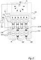
- Figure 2 illustrates a simplified cross-sectional view of the elements of the exposure system ES.
- the elements of the exposure system ES are an illumination source IS and an illumination unit IU.
- the illumination source IS comprises at least one light-emitting diode LD and a reflector (not illustrated).
- the illumination source IS furthermore may comprise optics which may or may not be part of the input optics 10. This optics may e.g. be part of the collimation of the light from the light-emitting diode LD.
- Various illumination sources IS may be used combined or not with reflectors and optics or any combinations thereof.
- the light-emitting diode LD may, be located in a one to one relationship with the spatial light modulators SLM. Hence one light-emitting diode LD is illuminating at least part of the light modulators LM of the spatial light modulator SLM. Such one to one relationship may facilitate that the optical axis of the light-emitting diode OALD is coinciding with the optical axis of at least some of the input optics OAOP.
- the light-emitting diode LD is located above the spatial light modulator SLM so that at least part of the modulators LM of at least one spatial light modulators SLM are illuminated by light from the light-emitting diode LD.
- the illumination source IS hence the light-emitting diodes LD, may be located so that light guides may be necessary to transmit light from the light-emitting diode LD to at least part of the light modulators LM of the at least one spatial light modulator SLM.
- Such light guides may e.g. comprise optical fibres (e.g. made of polymer, plastic, glass etc.), optics, lens arrays, reflectors, etc.
- the light-emitting diode LD may be of any known type or any development thereof.
- the light emitting diode LD may be e.g. a laser diode, ultraviolet diode or any other light source emitting light in form of electromagnetic radiation.
- the spatial light modulator SLM establishes a plurality of individual light beams, illuminating a plurality of illumination spots ISP together forming an illumination area.
- illumination area an approximated plane as defined by a number of focus points also referred to as illumination spot ISP of the individual light beams.
- the illumination area may form an approximated plane on the surface of the light-sensitive material LSM according to a digital layer-wise representation of the three-dimensional object OB.
- the exposure system ES is curing the light-sensitive material LSM in a pattern according to the digital layer-wise representation thereby forming the three-dimensional object OB.
- the light-sensitive material LSM may be a determining factor for the choice of light-emitting diode LD.
- the light-sensitive material LSM is cured when exposed or illuminated with light of high intensity with wavelengths between 200- 100000nm.
- light with a wavelength center frequency between 300 and 400nm are the most optimal for curing the preferred type of light-sensitive material LSM.
- light with other than the mentioned wavelengths may be used if special light-sensitive material LSM is required.
- optics or the spatial light modulators SLM which may be damaged when exposed to light with certain wavelengths.
- the light-sensitive material LSM is also cured when it is exposed to broad-spectrum light e.g. from the diffuse light distribution in a room, because the diffuse light distribution of a room often also contains light with wavelengths at which the light-sensitive material LSM reacts. Curing of light-sensitive material LSM from such stray-light is not desirable because it is slow and not controllable.
- the intensity of the light emitted from the light-emitting diode LD may vary. The higher the intensity is, the shorter is the time that the light-sensitive material LSM has to be exposed to the curing light. Hereby the speed of the exposure system ES scanning over the light-sensitive material LSM may be faster. Of course other factors are also determining the scanning speed, such as the type of light-sensitive material LSM, response time in the spatial light modulators SLM. etc.
- the illumination unit IU comprises input optics 10, at least one spatial light modulator SLM and output optics 00. Hence light from the illumination source IS is collimated and focused by means of the input optics 10, patterned by the spatial light modulator SLM and focused on the light-sensitive material by the output optics 00.
- the light is focused on at least some of the apertures of the at least one spatial light modulator SLM.
- the at least one spatial light modulator SLM then establishes a pattern of light onto the output optics 00, which again focuses the patterned light onto illumination spots ISP on the light-sensitive material LSM.
- a pattern of light also includes the situation when all individual light modulators LM of the spatial light modulator SLM are in a position which either lets light through all apertures of the spatial light modulator SLM or does not let any light at all through the apertures of the spatial light modulator SLM.
- the stereolithography apparatus SA comprises more than 64 spatial light modulators SLM. It should be noted that the stereolithography apparatus SA is very flexible in relation to the amount of spatial light modulators SLM. Hence the number of spatial light modulators SLM may vary between 1 and e.g. up to more then 100.
- the individual spatial light modulators SLM may be combined in modules of four. Hence, when more than four spatial light modulators SLM are needed, more than one module are combined together forming the exposure system ES.
- the illumination source IS may be adapted to a module of spatial light modulators SLM, e.g. with illumination source modules of four light emitting diodes LD.
- Each spatial light modulator SLM comprises more than 500 individually controllable light modulators LM.
- spatial light modulators SLM with a number which differs, sometimes differs a lot, from the 500 individually controllable light modulators LM may be used.
- the figures only illustrate the spatial light modulators SLM with e.g. four light modulators even though, as mentioned, there may be more than 500.
- the input optics 10 may comprise a lens system including e.g. collimation optics CO, focus optics e.g. in form of a micro lens arrays ML, lenses, etc.
- a micro lens ML is a plate e.g. of glass on which a polymer layer is deposited. The polymer layer is then shaped in order to have one spherical surface just in front of one aperture of the spatial light modulator SLM.
- the collimation optics CO is used for directional aligning the light from the light-emitting diode LD; hence the light forming the output from the collimation optics CO is preferably parallel.
- the introduction of the collimation optics CO may introduce large optical losses to the exposure system ES.
- an unintentional filtering of the light from the light-emitting diode LD may be introduced.
- the effect of the mentioned losses and filtering may result in that not all of the light emitted from the light-emitting diode LD is present after the collimation optics CO. It is a well known problem in the art that the loss of light emitted from the light emitting area LE of a light emitting diode LD is above 50%.
- the input optics 10 may also include focus optics e.g. in form of an array of micro lenses ML.
- the function of the micro lenses ML is to focus the collimated light onto the at least one spatial light modulator SLM.
- the at least one spatial light modulator SLM comprises a plurality of apertures and it is onto or down through these apertures that the micro lenses ML are focusing the collimated light.
- the size of the apertures may be between 20-40 ⁇ m, but preferably 30 ⁇ m.
- Figure 2 illustrates an example where the input optics 10 only comprises one array of micro lenses ML and the collimation optics CO comprises only one optical component.
- the input optics may firstly collimate the light by a first stage of optical components (also referred to as collimation optics CO) and then focus the light by a second stage of optical components e.g. in form micro lenses ML.
- the optical components may be any combination of optical components such as e.g. mirrors or singlets, doublets or aspherics lenses etc.
- the collimation optics CO may comprise 4 lenses.
- One reason to implement the collimations optics CO and micro lenses ML is to optimize the efficiency of the light emitted from the light-emitting diode LD.
- at least part of the collimation optics CO and/or micro lenses ML may be included in the illumination source IS.
- the at least one spatial light modulator SLM may be used to pattern the collimated and focused light onto illumination spots ISP on the light-sensitive material LSM.
- the at least one spatial light modulator SLM comprises a plurality of individual light modulators LM also referred to as light switches, light valves, micro shutters etc.
- the individual controllable light modulators LM are controlled by a control unit CU.
- the control unit CU may control the exposure system ES according to the digital layer-wise representation of the three-dimensional object to be built.
- the illustrated control unit CU may control the light-emitting diode LD and the individual controllable light modulators LM of the at least one spatial light modulator SLM.
- Controlling the light-emitting diodes LD implies to turn the light-emitting diodes LD off if e.g. only a small part of an object or a small object is to be built, which does not require patterned light from at least one spatial light modulator SLM included in the exposure system ES.
- the controlling of the light modulators LM in the at least one spatial light modulators SLM may be done by addressing the light modulators LM according to the pattern.
- the pattern may represent one layer of the three-dimensional object to be built.
- the illustrated control unit CU may also control other part of the stereolithography apparatus SA than the exposure system ES.
- the control unit CU may be included in other control systems in relation to the stereolithography apparatus SA.
- the stereolithography apparatus SA may be provided with digital layer-wise descriptions of the three-dimensional object to be built.
- the layer-wise description of the three-dimensional object may include a support structure if the three-dimensional object requires support during the building process.
- the exposure system ES is scanned across the light-sensitive material LSM and the individual digital layer-wise descriptions of the three-dimensional object determines the pattern of light from the spatial light modulator SLM.
- the output optics OO focuses the patterned light from the spatial light modulator SLM onto one or more illumination spots ISP on the surface of the light-sensitive material LSM.
- the output optics OO may comprise more than one lens system e.g. more than one array of micro lenses ML.
- the illumination spots ISP may be focus points located on the surface of the light-sensitive material LSM. It should be noted that the illumination spots ISP also could be located beneath the surface of the light-sensitive material LSM.
- the size of an illumination spot ISP is between 80 and 120 ⁇ m, preferably 100 ⁇ m.
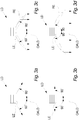
- Figure 3A-E illustrates principles of the light-emitting area LE of the light-emitting diode LD located in the illumination source IS.
- the illustrated embodiments on figure 3A-E are only to illustrate some of the possible principles behind the light-emitting diodes LD used in the illumination source IS.
- Each of the embodiments on figure 3A-E illustrates the light-emitting area LE, the part of the light-emitting diode LD which is emitting light.
- the preferred light-emitting diodes LD used in the illumination source IS has a cover (not illustrated) of e.g. a polymer, glass or plastic material, covering the light-emitting area LE.
- This cover may be used as pre-focusing and/or pre-collimating optics of the light emitted from the light-emitting area LE. Hence this cover may be part of the collimating optics CO described above e.g. in relation to figure 2 .
- Figure 3A illustrates an example, where the light-distributing angle of light emitted from the light-emitting area LE is 60 degrees from the optical axis of the light-emitting diode OALD.
- Figure 3B illustrates an example, where the light-distributing angle of light emitted from the light-emitting area LE is 90 degrees from the optical axis of the light-emitting diode OALD.
- Figure 3C illustrates an example, where the light-distributing angle of light emitted from the light-emitting area LE is 60 degrees from the optical axis of the light-emitting diode OALD and wherein a reflector RE is reflecting at least part of the light emitted from the light-emitting area LE. Inserting a reflector RE may serve to several purposes. First of all the reflector RE helps to direct the light emitted from the light-emitting area LE at least partly in the same direction. Hence the reflector may be seen as a pre-aligning or pre-collimating means of the light from the light-emitting area LE.
- a reflector RE may be shaped or designed to reflect the light from the light-emitting area LE in certain directions which may facilitate the further treatment of the light. Moreover the use of a reflector RE may reduce the stray-light incoming from the back side of the light emitting diode LD.
- Figure 3D illustrates an example where the light-distributing angle of light emitted from the light emitting area LE is 90 degrees from the optical axis of the light-emitting diode OALD and wherein a reflector RE is reflecting at least part of the light emitted from the light-emitting area LE.
- Figure 3E illustrates an example where light is emitted from both sides of the light-emitting area LE in light distributing angles up to 90 degrees from the optical axis OALD.
- An area AE is illustrated where no light is emitted from the light-emitting area LE, which is just to indicate that it may be very difficult to build a light-emitting diode LD emitting light from the lateral sides SI of the light-emitting area LE. If such light-emitting diode is built, it would be possible to utilise at least part of the light emitted from the side SI of such light-emitting diode.
- the light emitting center LE of the light emitting diode LD is located as close as possible to the focus point of the reflector RE.
- the implementation of the reflector may provide an optimized utilization of the light emitted from the light-emitting area LE of the light-emitting diode LD.
- more photons per added amount of power e.g. measured in mW, mA, mV, etc. may be utilised from the light-emitting diode LD.
- the reflector RE may be an integrated part of the light-emitting diode LD or the reflector RE may be placed external to the light-emitting diode LD. In the latter case the reflector RE may be part of the illumination source IS. Furthermore note that not all of the reflected light may be parallel as could be interpreted from the figures.
- the illumination source IS may comprise a light-emitting diode LD with an internal reflector which together with a reflector external to the light-emitting diode LD are reflecting the light emitted from the light-emitting diode LD.
- the light-distributing angle of light emitted from the light-emitting diode LD may vary from the mentioned 60 and 90 degrees. Hence the light-distributing angle is smaller e.g. down to 30 or even 10 degrees from the optical axis of the light-emitting diode OALD.
- optics may be inserted immediately after the light-emitting diode e.g. as part of the illumination source IS.
- Such optical elements may preferably be part of the collimation optics CO collimating the light from the light-emitting diode LD, but may also simply be used for focusing the light from the light-emitting diode LD.
- the illumination source IS including the light-emitting diode LD and e.g. optics is mounted on a printed circuit board PCB as illustrated on figure 4 .
- the illustration on figure 4 is only illustrating one way of carrying out the implementing of the illumination source IS in the stereolithography apparatus SA.
- At least one light-emitting diode LD is mounted on the printed circuit board PCB together with electronics EL, cooling means CM and at least one socket SO for supplying the printed circuit board PCB with control signals and/or power.
- the printed circuit board PCB may comprise the power supplies to the at least one light-emitting diode LD located on the printed circuit board PCB. Furthermore at least part of the control electronics for controlling e.g. the current or the voltage supplied to the light-emitting diodes LD may also be located on the printed circuit board PCB.
- the printed circuit board PCB also comprises sockets SO. This facilitates easy removal of wires W e.g. supplying the printed circuit board PCB with power- or control signals, hence easy removal of the printed circuit board PCB from the stereolithography apparatus SA. This could e.g. be advantageous in the situation where some of the electronics EL is damaged and the printed circuit board PCB is to be changed or repaired.
- heat H When the light-emitting diodes LD are emitting light they are producing heat H; hence it may be necessary to provide the printed circuit board PCB with cooling means CM to prevent from damaging the components mounted on or in relation to the printed circuit board PCB. Furthermore heat H from the light-emitting diodes LD may also cause structural changes in different material such as e.g. in iron, which is expanding when it is heated, having impact on the precision of the system.
- the cooling means CM may be a combination of different arrangements working together to optimize the cooling of the components mounted on the printed circuit board PCB.
- One arrangement could be one or more cooling surfaces CS optimized for transporting heat H away from the printed cooling board PCB.
- the one or more cooling surfaces CS may furthermore be provided with a fan FA circulating the air between the one or more cooling surfaces CS.
- An additional arrangement for removing heat H e.g. from the one or more light-emitting diodes LD is cooling channels CC through the printed circuit board PCB from the one or more light-emitting diodes LD to the cooling surfaces CS.
- Other cooling arrangements or elements than the above mentioned may be applied to the cooling means CM to optimize the removal of heat H from the components on the printed circuit board PCB.
- Such further elements could e.g. be cooling paste, water or metal for removing the heat H away from the printed circuit board PCB.
- some Peltier modules may be used in relation to the cooling means CM in order to control the temperature of /on the printed circuit board PCB. It should be noted that one or more Peltier modules may be enough to control the temperature of / on the printed circuit
- printed circuit board may be improved with printed circuit board guiding means PCBG.
- PCBG printed circuit board guiding means
- These printed circuit board guiding means PCBG are only optional and whether or not these printed circuit board guiding means PCBG form part of the printed circuit board PCB, if they are necessary and their exact location on the printed circuit board PCB depend on the system or method of mounting the printed circuit board PCB in the exposure system ES. This is disclosed in more details in relation to figure 7A and 7B .
- Examples on an illumination unit and a method of point illumination of a medium comprising a plurality of light emitters in the form of light guides which are arranged to illuminate at least one illumination face via a light valve arrangement can be seen e.g. from WO 98/47042 ,
- This apparatus comprises at least one light source for illumination of a cross-section of the light-sensitive material by at least one spatial light modulator of individually controllable light modulators, wherein at least one light source is optically coupled with a plurality of light guides arranged with respect to the spatial light modulator arrangement in such a manner that each light guide illuminates a sub-area of the cross-section.
- Figure 5A-C illustrates an example where the exposure system ES takes advantages of light from the light emitting diode LD emitted up to 90 degrees from the optical axis of the light emitting diode OALD.
- the scope is to utilise as much as possible of the light emitted from the light emitting diode LD.
- the light distribution angle of the light from the light emitting area LE of the light emitting diode LD may vary according to which type of light emitting diode is used in the illumination source IS. Hence some types of light emitting diodes LD may emit very focused light e.g. with a light distributions angle below 20 degrees from the optical axis of the light emitting diode OALD. Other types of light emitting diodes LD may on the other side emit diffuse light with a light distribution angle above 60 degrees from the optical axis of the light emitting diode OALD.
- the light emitting area LE emitting focused light e.g. with a light distributions angle below 20 degrees from the optical axis of the light emitting diode OALD, is used in the exposure system ES. It is therefore possible for a person skilled in the art to exploit the majority of the emitted light.
- Figure 5A illustrates the illumination source IS where light from the light emitting area LE is directed directly from the light emitting area LE towards a first optical lens OP. Since the light from the light emitting diode LD is relatively focused when emitted it may not be necessary to include any aligning optics shaping the light before the light enters the collimation optics.
- the first optical lens OP may therefore be part of the collimation system, collimating the light from the light emitting diode LD. Hence the losses in light are minimized, such losses could e.g. originate in reflectors, optics etc. because of the simple construction of the exposure system ES.
- the wider light distribution angle is, the more complicated is to exploit the majority of light emitted from the light emitting diode LD.
- the light emitting diode LD is emitting light in a light distribution angle above e.g. 60 degrees from the optical axis of the light emitting diode OALD, actions have to be taken to exploit at least some of the light.
- Such actions could e.g. be including one or more reflectors, optics, etc. as illustrated on figure 5B .
- a reflector is guiding at least part of the light from the light emitting area LE towards a first optical lens OP.
- This first optical lens OP may e.g. be focusing optics, collimation optics, etc.
- the illumination sources IS illustrated on figure 5A and 5B may be two among a plurality of different systems adapted to align light from the light emitting diode LD towards the first optical lens OP.
- other illumination sources IS may be used including protection P of the light emitting diode LD as part of the aligning / guiding of light towards the input optics 10.
- the choice of which illumination source IS is preferred depends on the choice of light emitting diode LD and any combinations of optics, reflectors, light guides etc. may be used to optimize the amount of usable light from the light emitting diode LD.
- the reflector RE illustrated on figure 5B and 5C may be internal or external in relation to the light emitting diode. Furthermore a combination of internal and external reflectors RE may be used to optimize the utilisation of the light from the light emitting diode LD.
- the illumination source IS illustrated on figure 5C comprises a combination of the protection P of the light emitting area LE, reflector RE and the first optics for directionally aligning the light.
- the example illustrated on figure 5C illustrates that the directional aligned light is directed towards the input optics 10.
- the input optics 10 comprises one or more collimation lenses illustrated as collimation optics CO and focusing optics in form of at least one micro lens array ML.
- the at least one micro lens array ML are focusing the collimated light through the spatial light modulator SLM, which by means of individual controllable light modulators LM establish a pattern of light.
- This pattern of light is by means at least one array of micro lenses ML directed in the output optics 00.
- the output optics then focuses the patterned light into illumination spots ISP on the surface of the light-sensitive material LSM.
- a control unit CU is controlling the light emitting diode LD and the spatial light modulator SLM.
- Figure 6 illustrates a second example facilitating measuring and control of the individual light emitting diode LD comprised in the illumination source IS. It is an important factor in building three-dimensional objects, especially when these three-dimensional objects cover a large area (e.g. 100-300cm 2 ), that the light-sensitive material LSM is illuminated with light having the same intensity. If the light-sensitive material LSM is not illuminated with light having the same intensity, the layers of light-sensitive material LSM are not uniformly cured.
- the scanning speed is partly depending on the amount of light received by the light-sensitive material LSM, the scanning speed can be increased if the intensity of the emitted light is increased. Hence the higher the intensity of light is, the faster the exposure system ES can be scanned across the light-sensitive material LSM.
- first illumination source 1IS and a second illumination source 2IS.
- the two illustrated illumination sources 1IS and 2IS would be part of a module comprising four illuminations units IU and four illumination sources IS. Furthermore more than one module would be coupled together forming a scanning bar.
- the first illumination source 1IS are illuminating the first illumination unit 1IU which again illuminates a measuring unit MU.
- the spatial light modulator SLM illustrated on figure 6 have all illustrated light modulators LM in a position letting light through the spatial light modulator SLM, to let as much of the light emitted from the illumination source IS as possible be received by the measuring unit MU.
- the measuring unit MU may be based on any light receiving sensor or light-sensitive material electrical coupled to the control unit CU.
- the measuring unit MU is measuring one or more representative values of the light from the light emitting diodes LD.
- the representative value may e.g. be a representation of the wavelength, intensity, position and size of the illumination spot ISP, etc.
- the representative value is then used as basis for controlling the individual light emitting diodes LD.
- Excluding light emitting diodes LD from the measuring and control procedure saves time and thereby the stereolithography apparatus SA becomes more efficient.
- the light emitting diodes LD which are to be used may be adjusted to emit light with a higher intensity and hence it becomes possible to increase the scanning speed and thereby the time for building a three-dimensional object.
- the measuring unit MU receives as much light from the light emitting diode LD of the illumination source IS as possible. This should not be confused with adjusting the light emitting diode LD to illuminate with the highest possible intensity e.g. by turning up the voltage or current applied to the light emitting diode LD.
- control unit CU may control the intensity and also the wavelength of the light from the light emitting diode LD by controlling the current or voltage applied to the light emitting diode LD.
- a control profile based on change of wavelength in relation to change of applied voltage or current may be provided.
- the exposure system may comprise several light emitting diodes each illuminating part of a layer of a three-dimensional object to be build.
- each individual light emitting diode LD has to be adjusted and / or regulated.
- One way of achieving this is to measure the intensity of the light received from the light emitting diode.
- each individual light emitting diode LD is adjusted so that all measured light emitting diodes LD are emitting light with the same intensity.
- Both the measuring and the adjustment / regulating of the light emitting diodes LD is controlled be means of a control unit CU.
- the control unit may comprise a data processor or control circuit which may perform the adjustment / regulating basing on different regulating algorithms such as e.g. proportional, integral and/or derivative or any combination thereof.
- the measuring unit MU may be implemented so that light from all the individual light emitting diodes LD can be measured by the measuring unit MU.
- the measuring unit MU it is possible to implement the measuring unit MU in such a way that not all light from all light emitting diodes LD is received. But a better result would be obtained, if the measuring unit is implemented according to what above. It should be noted that measuring light from all the light emitting diodes LD may not be done at the same time.
- the measuring unit may be mounted in the recoater REC (not shown). For each cured layer of light-sensitive material LSM the recoater REC is scanned perpendicular the scanning direction of the exposure system ES, hence the measuring unit is then, without any waste of time, scanning the individual light emitting diodes LD as the recoater REC recoats the new layer.
- the measuring apparatus may only be adapted to measure light from one light emitting diode at the time.
- one or more measuring units MU e.g. one or more light-sensitive sensors have to be used.
- the measuring unit MU may, be mounted right underneath the location where the exposure system ES is parked when the recoater REC recoats a new layer of light-sensitive material LSM. This facilitates that a measuring can be made between each layer to be cured.
- the measuring unit MU may then either be formed as a light-sensitive plate adapted to receive light from all light emitting diode LD at the same time.
- the measuring unit may comprise one or more light-sensitive sensors which are scanned under the exposure system ES. The number of sensors may be determined by the number of scans of the light-sensitive sensors underneath the exposure system ES.
- the diameter of the light-sensitive sensor has to be at least 9 mm to be able to measure all light from one spatial light modulator SLM
- the exposure system ES or the measuring unit MU comprises means for avoiding light from the exposure system to illuminate the light-sensitive material LSM when measuring the intensity of the light from the light emitting diode LS. This is done to reduce the amount of stray-light which is undesirable because it performs an uncontrollable curing of the light-sensitive material LSM.
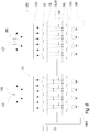
- Figure 7A and 7B illustrates a third example facilitating removal of the printed circuit board PCB.
- the printed circuit board PCB illustrated on figure 7A and 7B is similar to the printed circuit board PCB described in relation to figure 4 . Note that only an illumination source IS including a light emitting diode LD are illustrated on the printed circuit board PCB in relation to figure 7A and 7B .
- One module comprises four illumination sources IS and four illumination units IU.
- the third example illustrated on figure 7A discloses four illumination units and a printed circuit board PCB comprising four illumination sources IS. It is advantageous to be able to exchange at least one of the light emitting diodes LD, simply because the life time of the stereolithography apparatus SA may be several times the life time of a light emitting diode LD.
- the light emitting diode LS is mounted on a printed circuit board PCB; in relation to this aspect of the invention it may furthermore be advantageous to be able to exchange the whole printed circuit board PCB.
- Each of these electrical components, including the light emitting diodes LD, represents a potential source of failure for the exposure system ES. In case just one of the electrical components fails the exposure system ES may not operate optimally, hence this electrical component or even the whole printed circuit board PCB must to be changed.
- the releasable locking mechanism RLM may at least partly be located on a light source bed LSB. Other guidance means for facilitating securing the printed circuit board PCB may be located on the printed circuit board PCB.
- the light source bed LSB may e.g. be part of the casing / cover protecting the exposure system ES.
- Figure 7A illustrates a side view of an example.
- the light source bed LSB may be equipped with at least one but preferably four releasable locking mechanisms (only two are shown). Only one releasable locking mechanism RLM may be enough to secure the printed circuit board PCB to the light source bed LSB.
- the printed circuit board guidance means PCBG on the printed circuit board PCB may be shaped as a protruding part e.g. in form of a pawl.
- the light source bed guidance means LSBG on the light source bed LSB may be shaped as holes in the light source bed LSB adapted to receive the protruding part of the printed circuit board guidance means PCBG.
- the illustrated releasable locking mechanism RLM is only one way of securing the printed circuit board PCB to the light source bed LSB.
- the light source guidance means LSBG may e.g. be a recess or a hole in any geometrical form.
- the protruding part illustrated as the printed circuit board guidance means PCBG is located on the printed circuit board PCB or on the light source bed LSB.
- Figure 7B illustrates a top view of an example, where a printed circuit board PCB is partly connected to a light source bed LSB.
- the releasable locking mechanisms RLM are movable connected to the light source bed LSB.
- the releasable locking mechanisms RLM may e.g. be turned thereby overlapping or covering at least a part of the printed circuit board PCB.
- the printed circuit board PCB is secured to the light source bed LSB as illustrated on the left side LS of the printed circuit board PCB.
- the two releasable locking mechanisms RLM are turned so that they are not overlapping or covering part of the printed circuit board PCB.
- the illustrated releasable locking mechanism RLM is only one way of securing the printed circuit board PCB to the light source bed LSB.
- the releasable locking mechanisms RLM may e.g. turn both ways, be removable e.g. by means of a latch/notch system or screw system.
- it may not be important e.g. if the movable part of the releasable locking mechanism RLM is located on the printed circuit board PCB or on the light source bed LSB.
- the printed circuit board PCB is located on the top of the light source bed LSB and not as illustrated in figure 7A lowered into the light source bed LSB. There may be various locking systems adapted to lock the printed circuit board PCB to the light source bed LSB.
- a common denominator for all locking systems which is suitable for the present exposure system ES is that, when the printed circuit board PCB is locked/secured to the light source bed LSB, the optical axis of the light emitting diode OALD is coincident with the optical axis of the input optics OAOP.
- the maximal angle between the rays of light from the light emitting diode LD and the optical axis of at least part of the input optics OAOP is 1,5 degrees or lower.
- the exposure system ES may not be operated optimally. In some situations the effect of such misalignment of the optical axes may not be worth to be considered. In other situations the deviation between the two optical axes may be at least partly corrected by performing a post-adjustment or calibration of one of the optical axes. Such post-adjustment may e.g. be performed mechanically or electrically.
- the illuminations units IU comprises input optics 10 with one or more collimation lenses illustrated as collimation optics CO and focusing optics in form of at least one micro lens array ML.
- the at least one micro lens array ML is focusing the collimated light through the spatial light modulator SLM, which by means of individually controllable light modulators LM establishes a pattern of light. This pattern of light is directed in the output optics 00 by means of at least one array of micro lenses ML. The output optics then focuses the patterned light onto illumination spots ISP on the surface of the light-sensitive material LSM.
- a control unit CU is controlling the light emitting diode LD and the spatial light modulator SLM. Furthermore the control unit may control the post-adjustment of one or both of the optical axes if necessary.
- FIG 8-10 illustrates only one possible embodiment of the stereolithography apparatus SA, it should be noted that not all below mentioned features are necessary for the stereolithography apparatus SA to operate. Furthermore it should be noted that not all details of the stereolithography apparatus SA are illustrated and that additional, not illustrated, parts may be advantageous.
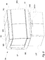
- FIG 8 illustrates the stereolithography apparatus SA in a front / side view according to an aspect of the invention.
- the stereolithography apparatus SA may be equipped with one or more sliding vat doors SVD, which may e.g. be opened by means of a sliding vat door handle SVDH which is activated e.g. by pushing, turning, etc.
- the sliding vat door SVD may give access to the vat V (not shown) by means of sliding to one side or by means of pivoting around one or more hinges.
- One or more sliding front doors SFD may be positioned in relation to one or more front panels FP and side panels SP.
- the sliding front door SFD may give access to the exposure system ES (not shown) by means of sliding to one side or by means of pivoting around one or more hinges.
- the sliding front doors SFD may be transparent so that the building process can be monitored without opening the sliding front door SFD.
- the one or more front panels FP may extend to the side of the stereolithography apparatus SA.
- the one or more front panels FP may be equipped with one or more machine status indicators MSI, indicating the status (e.g. in operation, stopped, fault, etc.) of the machine or at which stage in a building process the stereolithography apparatus SA is at a given time.
- the machine status indicator MSI may also be located on the roof RO or side of the stereolithography apparatus SA and it may e.g. comprise a display, lamps, sirens etc.
- stereolithography apparatus SA may be equipped with one or more side doors SID and one or more lower side panel LSP, which are not in use under normal operation of the stereolithography apparatus SA.
- the side doors SID and the lower side panel LSP are only dismounted or opened when parts of the stereolithography apparatus SA are to be maintained.
- side doors SID may be part of the sliding front door SFD and the lower side panel LSP may be part of the sliding vat door SVD.
- Figure 9 illustrates the stereolithography apparatus SA in a back / side view where the side door SID and the sliding front door SFD are dismounted revealing the exposure system ES.
- the stereolithography apparatus SA may stand on one or more machine feet MF, which may be adjustable. This may make easier installing the stereolithography apparatus SA so that when the vat V (not shown) is located in the stereolithography apparatus SA the surface of the light-sensitive material LSM and the output optics OP (not shown) are substantially parallel.
- the illustrated exposure system ES comprises an upper left side door UD and a lower left side door LD used when maintaining or servicing the exposure system ES. Furthermore the exposure system comprises a lamp housing door LHD for accessing the illumination source IS (not shown). Furthermore the exposure system ES comprises a protection plate PP for protecting the different parts of the illumination unit IU (not shown). The side of the protection window PW is also illustrated on figure 9 together with the outer frame of the exposure bar OFEB
- a handle HD for releasing the protection window PW may be located in the exposure system casing ESC.
- Figure 10 illustrates the stereolithography apparatus SA in a front view where the sliding front door SFD is removed.
- the exposure system ES is moving in a exposure system carriage slit ESCS, when scanning across the light-sensitive material LSM (not shown).
- figure 10 illustrates the machine frame MFR around which the machine is build up and a support base for exposure system energy chain SBEC.
- the present invention exhibits notable and unexpected advantages for the infra red powder sintering of materials, whereby large surfaces can be rapidly treated with high precision.
Landscapes
- Engineering & Computer Science (AREA)
- Chemical & Material Sciences (AREA)
- Materials Engineering (AREA)
- Manufacturing & Machinery (AREA)
- Physics & Mathematics (AREA)
- Mechanical Engineering (AREA)
- Optics & Photonics (AREA)
- Health & Medical Sciences (AREA)
- Toxicology (AREA)
- Oral & Maxillofacial Surgery (AREA)
- Thermal Sciences (AREA)
- Exposure And Positioning Against Photoresist Photosensitive Materials (AREA)
- Exposure Of Semiconductors, Excluding Electron Or Ion Beam Exposure (AREA)
Description
- The invention relates to improvements relating to a rapid prototyping apparatus for the manufacturing of three-dimensional objects by additive treatment of cross-sections.
- Apparatuses for use in stereolithography have been developed over the recent years. They now include both UV-light bulbs and light emitting diodes as light sources. Document
US 2008/0157412 A1 relates to an optical modeling apparatus, comprising two light sources, a spatial light modulator, input and output optics and a control unit. Implementing light emitting diodes as light source leads to different problems, which are dealt with in this application. - The invention relates to a stereolithography apparatus with an exposure system, said exposure system comprising at least one printed circuit board with at least one socket and at least one light emitting diode, at least two spatial light modulators with a plurality of individually controllable light modulators, input optics optically coupled to said spatial light modulators, output optics optically coupled to said spatial light modulators, at least one control unit, at least one light source bed releasably locking said printed circuit board in such a way that the optical axis of the light emitting diode is aligned with the optical axis of said input optics, wherein said input optics and output optics facilitate transmission of light emitted from said light emitting diodes via said individually controllable light modulators of said spatial light modulators to an illumination area, wherein said spatial light modulators enable an establishment of a pattern of the light from said input optics, according to control signals from said control unit, wherein said output optics enables focusing of the pattern of light from said spatial light modulators onto an illumination area.
- It is possible to exchange the light emitting diodes. The life time of the whole stereolithography apparatus is several times the life time of the light emitting diodes, hence exchange of the light emitting diodes is necessary.
- The light source bed is part of the exposure system e.g. including at least some of the input optics and hence is not easy to remove from the stereolithography apparatus. Hence it is very advantageous to be able to remove the light emitting diodes from the light bed without removing the light source bed itself.
- More than one spatial light modulator are used e.g. to increase the width of the exposure system and thereby to increase the area which is possible to illuminate; hence it is possible to build larger objects or a larger number of small objects at the same time.
- The light emitting diodes are easier to handle if one or more of the light emitting diodes are connected to a printed circuit board. It may be easier and faster to exchange a printed circuit board comprising e.g. four light emitting diodes compared to exchanging four individual light emitting diodes.
- In an embodiment of the invention said printed circuit board is releasably locked to said light source bed by means of a releasable locking mechanism, wherein said printed circuit board is releasable locked by means of said releasable locking mechanism in such a way that the optical axis of said at least one light emitting diode is coinciding with the optical axis of said input optics.
- The high requirements for precision in the exposure system are met by a light source bed comprising a releasable locking mechanism. Hence when the light emitting diode is placed in the light source bed, the optical axis of the light emitting diode is aligned with the optical axis for the input optics within a given tolerance and locked in this position by means of the releasable locking mechanism.
- No further alignment or adjustment is required for the optical axis of the light emitting diode attached to the printed circuit board to be coincided with the optical axis of the input optics when the printed circuit board is releasably locked to said light source bed.
- It is easy and fast to change the printed circuit board, when it is releasably locked to the light source bed by means of the releasable locking mechanisms.
- In an embodiment of the invention said stereolithography apparatus comprises an alarm for indicating malfunction or abnormalities in operation of the apparatus.
- An alarm may indicate when it is time to change one or more of the light emitting diodes. The alarm could e.g. be in form of a sound, light (e.g. flashing or rotating), electronic data alarm etc. An alarm may be very advantageous because then the light emitting diodes are not changed without reason and no need for service personnel to check e.g. the intensity of the light emitting diodes is needed.
- Service personnel may by means of e.g. a computer check the light emitting diodes, e.g. how many hours they have been used, the present intensity etc; this may be very advantageous for the service personnel in order to plan maintenance of parts of the stereolithography apparatus.
- In an embodiment of the invention said at least one printed circuit board comprises cooling means comprising at least one cooling surface.
- A cooling surface may be attached to the printed circuit board to facilitate cooling of the electronics on the printed circuit board to reduce the risk of damaging the electronics or the printed circuit board.
- The cooling surface may be provided with a fan for optimizing the removal of heat from the printed circuit board.
- Holes may be made through the printed circuit board to optimize the removal of heat from one side of the printed circuit board to the other side of the printed circuit board.
- In an embodiment of the invention said releasable locking mechanism is movably connected to said light source bed.
- It may be possible to turn or in any other way to move the releasable locking mechanism from one position to another. This is advantageous when the printed circuit board is to be inserted or removed from the light source bed.
- It may be possible to remove the releasable locking mechanism from the light source bed.
- In an embodiment of the invention the error of alignment of the optical axis of the light emitting diode and the optical axis of the input optics is smaller than 20µm.
- In an embodiment of the invention said light source bed, said exposure system or said printed circuit board comprise an adjusting mechanism for adjusting the position of the optical axis of said at least one light emitting diode or of the optical axis of said input optics.
- The invention the light source bed may be provided with a mechanism for adjusting the printed circuit board or the printed circuit board may be provided with a mechanism for adjusting the light emitting diode manually or electrically. When e.g. a light emitting diode or a printed circuit board is exchanged and e.g. a measuring reveals that the optical axis of the light emitting diode is not completely coinciding with the optical axis of the input optics, it may be advantageous to be able to calibrate the light emitting diode or the printed circuit board until coincidence of the two optical axis occurs. Alternatively elements of the exposure system may be adjusted such as the input and or output optics.
- Furthermore the invention relates to a method of manufacturing three-dimensional objects from a light-sensitive material by the use of an apparatus according to any of the claims 1-9.
- In an embodiment of the invention the number of light emitting diodes is equal to or less than the number of spatial light modulators.
- One specific light emitting diode may be dedicated to one specific spatial light modulator. This may be very advantageous because it then becomes possible to completely turn off one light emitting diode if patterned light from one of the spatial light modulators does not have to be use to build one layer of an object. Turning off one light emitting diode reduces the energy consumption as well as the production of heat.
- In an embodiment of the invention the apparatus comprises light guiding means for guiding light emitted from one or more of said light emitting diodes to said spatial light modulators, said light guiding means being in the form of optical fibers
- The invention will now be described more in detail with reference to the figures of which
-
fig. 1 illustrates a simplified cross-sectional view of a stereolithography apparatus, -
fig. 2 illustrates an exposure system, -
fig. 3A-E illustrates a simplified cross-sectional view of the illumination source of the exposure system, -
fig. 4 illustrates a simplified cross-sectional view of a printed circuit board comprising the illumination source, -
fig. 5A-C illustrates one example of aligning light from a light emitting diode, -
fig. 6 illustrates one example of measuring and controlling the exposure system, -
fig. 7A-B illustrates one example of exchanging the light emitting diodes, -
fig. 8 illustrates an example of a stereolithography apparatus according to an aspect of the invention, -
fig. 9 illustrates a further example of a stereolithography apparatus according to an aspect of the invention, and -
fig. 10 illustrates a further example of a stereolithography apparatus according to an aspect of the invention. - In using an apparatus according to the present invention for the manufacture of three-dimensional objects a light-sensitive material LSM is used as the material forming the object. A person skilled in the art will know of various types of light-sensitive material suitable for this purpose.
-
Figure 1 illustrates a simplified cross-sectional view of a stereolithography apparatus SA for building three-dimensional objects OB according to one aspect of the present invention. The three-dimensional objects OB are built layer-wise through the curing of light-sensitive material LSM when exposed to light from the exposure system ES. - The stereolithography apparatus SA comprises a building plate BP on which one or more three-dimensional objects OB are build. The building plate BP is moved vertically into a vat V comprising light-sensitive material LSM by means of an elevator EL. A recoater REC is scanned across the new layer of light-sensitive material LSM to ensure uniformity of the new layer.
- According to the above description the three-dimensional object OB is built by exposing a layer of light-sensitive material LSM with patterned light from the exposure system ES. A layer of the light-sensitive material LSM is cured according to the pattern of light to which it is exposed. When a first layer is cured, the building plate BP with the cured first layer of the three-dimensional object OB is lowered into the vat V and the recoater REC scans across the layer of light-sensitive material LSM in order to establish a fresh upper layer of light-sensitive material LSM. Then the exposure system ES is again scanned across the light-sensitive material LSM curing a new layer of the three-dimensional object OB.
- As mentioned, the stereolithography apparatus SA comprises an exposure system ES. The exposure system ES comprises an illumination source IS (not illustrated) and an illumination unit IU (not illustrated). At least part of the exposure system ES is scanned across the light-sensitive material LSM in a scanning direction SD.
- The vat V may be equipped with means for moving the vat V such as wheels, interactions with a rail, track, forklifts etc. Hence the vat V may be removable located in the stereolithography apparatus SA, which is accessible via an opening OP, e.g. to refill the vat V with light-sensitive material LSM or for easy removal of three-dimensional objects OB from the building plate BP.
- It should be noted that it is possible, e.g. by means of the illustrated elevator EL or other devices, to move the vat V vertically instead of moving the building plate BP.
- The digital layer-wise representation of the three-dimensional object OB may be provided to the stereolithography apparatus SA via an interface unit IFU. The interface unit IFU may comprise input interfaces, such as e.g. a keyboard or pointer and output interfaces such as e.g. a screen or a printer, to handle communication via interfaces such as e.g. LAN (LAN; Local Area Network), WLAN (WLAN; Wireless Local Area Network), serial communication etc. Furthermore the interface unit IFU may comprise data processors, memories and/or means for permanent storing of data.
-
Figure 2 illustrates a simplified cross-sectional view of the elements of the exposure system ES. The elements of the exposure system ES are an illumination source IS and an illumination unit IU. - The illumination source IS comprises at least one light-emitting diode LD and a reflector (not illustrated). The illumination source IS furthermore may comprise optics which may or may not be part of the
input optics 10. This optics may e.g. be part of the collimation of the light from the light-emitting diode LD. Various illumination sources IS may be used combined or not with reflectors and optics or any combinations thereof. - The light-emitting diode LD may, be located in a one to one relationship with the spatial light modulators SLM. Hence one light-emitting diode LD is illuminating at least part of the light modulators LM of the spatial light modulator SLM. Such one to one relationship may facilitate that the optical axis of the light-emitting diode OALD is coinciding with the optical axis of at least some of the input optics OAOP.
- The light-emitting diode LD is located above the spatial light modulator SLM so that at least part of the modulators LM of at least one spatial light modulators SLM are illuminated by light from the light-emitting diode LD.
- The illumination source IS, hence the light-emitting diodes LD, may be located so that light guides may be necessary to transmit light from the light-emitting diode LD to at least part of the light modulators LM of the at least one spatial light modulator SLM. Such light guides may e.g. comprise optical fibres (e.g. made of polymer, plastic, glass etc.), optics, lens arrays, reflectors, etc.
- The light-emitting diode LD may be of any known type or any development thereof. The light emitting diode LD may be e.g. a laser diode, ultraviolet diode or any other light source emitting light in form of electromagnetic radiation.
- The spatial light modulator SLM establishes a plurality of individual light beams, illuminating a plurality of illumination spots ISP together forming an illumination area.
- Within the context of this description and the appended claims, with the term "illumination area" is meant an approximated plane as defined by a number of focus points also referred to as illumination spot ISP of the individual light beams.
- The illumination area may form an approximated plane on the surface of the light-sensitive material LSM according to a digital layer-wise representation of the three-dimensional object OB.
- The exposure system ES is curing the light-sensitive material LSM in a pattern according to the digital layer-wise representation thereby forming the three-dimensional object OB.
- The light-sensitive material LSM may be a determining factor for the choice of light-emitting diode LD. Typically the light-sensitive material LSM is cured when exposed or illuminated with light of high intensity with wavelengths between 200-100000nm. Typically light with a wavelength center frequency between 300 and 400nm are the most optimal for curing the preferred type of light-sensitive material LSM. Of course light with other than the mentioned wavelengths may be used if special light-sensitive material LSM is required.
- Other factors may also be determining for the choice of light-emitting diodes LD.
Such factors could be e.g. the optics or the spatial light modulators SLM which may be damaged when exposed to light with certain wavelengths. One specific example is optics coated with a polymer and exposed either with light having a high intensity or with light having low intensity during a longer period of time; at wavelength under 250nm the lifetime of the optics may be decreased significantly. - It should be noted that the light-sensitive material LSM is also cured when it is exposed to broad-spectrum light e.g. from the diffuse light distribution in a room, because the diffuse light distribution of a room often also contains light with wavelengths at which the light-sensitive material LSM reacts. Curing of light-sensitive material LSM from such stray-light is not desirable because it is slow and not controllable.
- The intensity of the light emitted from the light-emitting diode LD may vary. The higher the intensity is, the shorter is the time that the light-sensitive material LSM has to be exposed to the curing light. Hereby the speed of the exposure system ES scanning over the light-sensitive material LSM may be faster. Of course other factors are also determining the scanning speed, such as the type of light-sensitive material LSM, response time in the spatial light modulators SLM. etc.
- The illumination unit IU comprises
input optics 10, at least one spatial light modulator SLM and output optics 00. Hence light from the illumination source IS is collimated and focused by means of theinput optics 10, patterned by the spatial light modulator SLM and focused on the light-sensitive material by the output optics 00. - The light is focused on at least some of the apertures of the at least one spatial light modulator SLM. The at least one spatial light modulator SLM then establishes a pattern of light onto the output optics 00, which again focuses the patterned light onto illumination spots ISP on the light-sensitive material LSM.
- It should be noted that a pattern of light also includes the situation when all individual light modulators LM of the spatial light modulator SLM are in a position which either lets light through all apertures of the spatial light modulator SLM or does not let any light at all through the apertures of the spatial light modulator SLM.
- The stereolithography apparatus SA comprises more than 64 spatial light modulators SLM. It should be noted that the stereolithography apparatus SA is very flexible in relation to the amount of spatial light modulators SLM. Hence the number of spatial light modulators SLM may vary between 1 and e.g. up to more then 100.
- The individual spatial light modulators SLM may be combined in modules of four. Hence, when more than four spatial light modulators SLM are needed, more than one module are combined together forming the exposure system ES. In relation hereto the illumination source IS may be adapted to a module of spatial light modulators SLM, e.g. with illumination source modules of four light emitting diodes LD.
- Each spatial light modulator SLM comprises more than 500 individually controllable light modulators LM. Of course spatial light modulators SLM with a number which differs, sometimes differs a lot, from the 500 individually controllable light modulators LM may be used. To simplify the figures, throughout this description the figures only illustrate the spatial light modulators SLM with e.g. four light modulators even though, as mentioned, there may be more than 500.
- The
input optics 10 may comprise a lens system including e.g. collimation optics CO, focus optics e.g. in form of a micro lens arrays ML, lenses, etc. One example of a micro lens ML is a plate e.g. of glass on which a polymer layer is deposited. The polymer layer is then shaped in order to have one spherical surface just in front of one aperture of the spatial light modulator SLM. - The collimation optics CO is used for directional aligning the light from the light-emitting diode LD; hence the light forming the output from the collimation optics CO is preferably parallel. The introduction of the collimation optics CO may introduce large optical losses to the exposure system ES. Furthermore an unintentional filtering of the light from the light-emitting diode LD may be introduced. The effect of the mentioned losses and filtering may result in that not all of the light emitted from the light-emitting diode LD is present after the collimation optics CO. It is a well known problem in the art that the loss of light emitted from the light emitting area LE of a light emitting diode LD is above 50%. For this reason it is important to be able to align and collimate the emitted light.
In the present description and the appending claims the term "parallel" shall not interpreted as parallel in a strict mathematical sense. Rather, the above term shall be interpreted as parallel having a precision within physical possible limits. - As explained, the
input optics 10 may also include focus optics e.g. in form of an array of micro lenses ML. The function of the micro lenses ML is to focus the collimated light onto the at least one spatial light modulator SLM. As explained below, the at least one spatial light modulator SLM comprises a plurality of apertures and it is onto or down through these apertures that the micro lenses ML are focusing the collimated light. The size of the apertures may be between 20-40 µm, but preferably 30 µm. -
Figure 2 illustrates an example where theinput optics 10 only comprises one array of micro lenses ML and the collimation optics CO comprises only one optical component. - The input optics may firstly collimate the light by a first stage of optical components (also referred to as collimation optics CO) and then focus the light by a second stage of optical components e.g. in form micro lenses ML. The optical components may be any combination of optical components such as e.g. mirrors or singlets, doublets or aspherics lenses etc.
- Of course different combinations of the type and number of micro lenses ML and collimation lenses CO may be used. The collimation optics CO may comprise 4 lenses. One reason to implement the collimations optics CO and micro lenses ML is to optimize the efficiency of the light emitted from the light-emitting diode LD. Furthermore it should be noted that at least part of the collimation optics CO and/or micro lenses ML may be included in the illumination source IS.
- The at least one spatial light modulator SLM may be used to pattern the collimated and focused light onto illumination spots ISP on the light-sensitive material LSM. The at least one spatial light modulator SLM comprises a plurality of individual light modulators LM also referred to as light switches, light valves, micro shutters etc.
- The individual controllable light modulators LM are controlled by a control unit CU. The control unit CU may control the exposure system ES according to the digital layer-wise representation of the three-dimensional object to be built. The illustrated control unit CU may control the light-emitting diode LD and the individual controllable light modulators LM of the at least one spatial light modulator SLM.
- Controlling the light-emitting diodes LD implies to turn the light-emitting diodes LD off if e.g. only a small part of an object or a small object is to be built, which does not require patterned light from at least one spatial light modulator SLM included in the exposure system ES.
- The controlling of the light modulators LM in the at least one spatial light modulators SLM may be done by addressing the light modulators LM according to the pattern. The pattern may represent one layer of the three-dimensional object to be built.
- The illustrated control unit CU may also control other part of the stereolithography apparatus SA than the exposure system ES. Alternatively the control unit CU may be included in other control systems in relation to the stereolithography apparatus SA.
- The stereolithography apparatus SA may be provided with digital layer-wise descriptions of the three-dimensional object to be built. The layer-wise description of the three-dimensional object may include a support structure if the three-dimensional object requires support during the building process. For each layer of the three-dimensional object, the exposure system ES is scanned across the light-sensitive material LSM and the individual digital layer-wise descriptions of the three-dimensional object determines the pattern of light from the spatial light modulator SLM.
- The output optics OO focuses the patterned light from the spatial light modulator SLM onto one or more illumination spots ISP on the surface of the light-sensitive material LSM. Like the
input optics 10, the output optics OO may comprise more than one lens system e.g. more than one array of micro lenses ML. - The illumination spots ISP may be focus points located on the surface of the light-sensitive material LSM. It should be noted that the illumination spots ISP also could be located beneath the surface of the light-sensitive material LSM.
- The size of an illumination spot ISP is between 80 and 120 µm, preferably 100 µm.
-
Figure 3A-E illustrates principles of the light-emitting area LE of the light-emitting diode LD located in the illumination source IS. The illustrated embodiments onfigure 3A-E are only to illustrate some of the possible principles behind the light-emitting diodes LD used in the illumination source IS. Each of the embodiments onfigure 3A-E illustrates the light-emitting area LE, the part of the light-emitting diode LD which is emitting light. - The preferred light-emitting diodes LD used in the illumination source IS has a cover (not illustrated) of e.g. a polymer, glass or plastic material, covering the light-emitting area LE. This cover may be used as pre-focusing and/or pre-collimating optics of the light emitted from the light-emitting area LE. Hence this cover may be part of the collimating optics CO described above e.g. in relation to
figure 2 . -
Figure 3A illustrates an example, where the light-distributing angle of light emitted from the light-emitting area LE is 60 degrees from the optical axis of the light-emitting diode OALD. -
Figure 3B illustrates an example, where the light-distributing angle of light emitted from the light-emitting area LE is 90 degrees from the optical axis of the light-emitting diode OALD. -
Figure 3C illustrates an example, where the light-distributing angle of light emitted from the light-emitting area LE is 60 degrees from the optical axis of the light-emitting diode OALD and wherein a reflector RE is reflecting at least part of the light emitted from the light-emitting area LE. Inserting a reflector RE may serve to several purposes. First of all the reflector RE helps to direct the light emitted from the light-emitting area LE at least partly in the same direction. Hence the reflector may be seen as a pre-aligning or pre-collimating means of the light from the light-emitting area LE. Secondly a reflector RE may be shaped or designed to reflect the light from the light-emitting area LE in certain directions which may facilitate the further treatment of the light. Moreover the use of a reflector RE may reduce the stray-light incoming from the back side of the light emitting diode LD. -
Figure 3D illustrates an example where the light-distributing angle of light emitted from the light emitting area LE is 90 degrees from the optical axis of the light-emitting diode OALD and wherein a reflector RE is reflecting at least part of the light emitted from the light-emitting area LE. -
Figure 3E illustrates an example where light is emitted from both sides of the light-emitting area LE in light distributing angles up to 90 degrees from the optical axis OALD. An area AE is illustrated where no light is emitted from the light-emitting area LE, which is just to indicate that it may be very difficult to build a light-emitting diode LD emitting light from the lateral sides SI of the light-emitting area LE. If such light-emitting diode is built, it would be possible to utilise at least part of the light emitted from the side SI of such light-emitting diode. - The light emitting center LE of the light emitting diode LD is located as close as possible to the focus point of the reflector RE.
- In relation to
figure 3C-3E the implementation of the reflector may provide an optimized utilization of the light emitted from the light-emitting area LE of the light-emitting diode LD. Hence in these embodiments more photons per added amount of power e.g. measured in mW, mA, mV, etc. may be utilised from the light-emitting diode LD. - The reflector RE may be an integrated part of the light-emitting diode LD or the reflector RE may be placed external to the light-emitting diode LD. In the latter case the reflector RE may be part of the illumination source IS. Furthermore note that not all of the reflected light may be parallel as could be interpreted from the figures.
- The illumination source IS may comprise a light-emitting diode LD with an internal reflector which together with a reflector external to the light-emitting diode LD are reflecting the light emitted from the light-emitting diode LD.
- Note that in relation to
figure 3A-3E the light-distributing angle of light emitted from the light-emitting diode LD may vary from the mentioned 60 and 90 degrees. Hence the light-distributing angle is smaller e.g. down to 30 or even 10 degrees from the optical axis of the light-emitting diode OALD. - Note that in relation to
figure 3A-3E only the light-emitting area LE of the light emitting-diode LD is illustrated; hence neither e.g. the fixation nor the galvanic connections are illustrated. - Note that in relation to
figure 3A-3E optics (not shown) may be inserted immediately after the light-emitting diode e.g. as part of the illumination source IS. Such optical elements (not shown) may preferably be part of the collimation optics CO collimating the light from the light-emitting diode LD, but may also simply be used for focusing the light from the light-emitting diode LD. - The illumination source IS including the light-emitting diode LD and e.g. optics is mounted on a printed circuit board PCB as illustrated on
figure 4 . The illustration onfigure 4 is only illustrating one way of carrying out the implementing of the illumination source IS in the stereolithography apparatus SA. - As illustrated, at least one light-emitting diode LD is mounted on the printed circuit board PCB together with electronics EL, cooling means CM and at least one socket SO for supplying the printed circuit board PCB with control signals and/or power.
- The printed circuit board PCB may comprise the power supplies to the at least one light-emitting diode LD located on the printed circuit board PCB. Furthermore at least part of the control electronics for controlling e.g. the current or the voltage supplied to the light-emitting diodes LD may also be located on the printed circuit board PCB.
- In the example where electronics EL is mounted on the printed circuit board PCB, it is preferred that the printed circuit board PCB also comprises sockets SO. This facilitates easy removal of wires W e.g. supplying the printed circuit board PCB with power- or control signals, hence easy removal of the printed circuit board PCB from the stereolithography apparatus SA. This could e.g. be advantageous in the situation where some of the electronics EL is damaged and the printed circuit board PCB is to be changed or repaired.
- It should be noted that of course it is possible to supply the printed circuit board PCB with power and or control signals without using sockets SO, one example could be mounting wires directly on the printed circuit board PCB.
- When the light-emitting diodes LD are emitting light they are producing heat H; hence it may be necessary to provide the printed circuit board PCB with cooling means CM to prevent from damaging the components mounted on or in relation to the printed circuit board PCB. Furthermore heat H from the light-emitting diodes LD may also cause structural changes in different material such as e.g. in iron, which is expanding when it is heated, having impact on the precision of the system.
- The cooling means CM may be a combination of different arrangements working together to optimize the cooling of the components mounted on the printed circuit board PCB.
- One arrangement could be one or more cooling surfaces CS optimized for transporting heat H away from the printed cooling board PCB. The one or more cooling surfaces CS may furthermore be provided with a fan FA circulating the air between the one or more cooling surfaces CS. An additional arrangement for removing heat H e.g. from the one or more light-emitting diodes LD is cooling channels CC through the printed circuit board PCB from the one or more light-emitting diodes LD to the cooling surfaces CS. Of course other cooling arrangements or elements than the above mentioned may be applied to the cooling means CM to optimize the removal of heat H from the components on the printed circuit board PCB. Such further elements could e.g. be cooling paste, water or metal for removing the heat H away from the printed circuit board PCB. Moreover some Peltier modules may be used in relation to the cooling means CM in order to control the temperature of /on the printed circuit board PCB. It should be noted that one or more Peltier modules may be enough to control the temperature of / on the printed circuit board PCB.
- Furthermore the printed circuit board may be improved with printed circuit board guiding means PCBG. These printed circuit board guiding means PCBG are only optional and whether or not these printed circuit board guiding means PCBG form part of the printed circuit board PCB, if they are necessary and their exact location on the printed circuit board PCB depend on the system or method of mounting the printed circuit board PCB in the exposure system ES. This is disclosed in more details in relation to
figure 7A and7B . - Examples on a method and an illumination unit for point illumination of a medium and how to collimate light and illuminate can be found e.g. in
WO 98/47048 - Examples on an illumination unit and a method of point illumination of a medium comprising a plurality of light emitters in the form of light guides which are arranged to illuminate at least one illumination face via a light valve arrangement can be seen e.g. from
WO 98/47042 - An example of a rapid prototyping apparatus for the manufacturing of three-dimensional objects by additive treatment of cross-sections comprising a wholly or partially light-sensitive material is described in
WO 00/21735 -
Figure 5A-C illustrates an example where the exposure system ES takes advantages of light from the light emitting diode LD emitted up to 90 degrees from the optical axis of the light emitting diode OALD. - The scope is to utilise as much as possible of the light emitted from the light emitting diode LD. The light distribution angle of the light from the light emitting area LE of the light emitting diode LD may vary according to which type of light emitting diode is used in the illumination source IS. Hence some types of light emitting diodes LD may emit very focused light e.g. with a light distributions angle below 20 degrees from the optical axis of the light emitting diode OALD. Other types of light emitting diodes LD may on the other side emit diffuse light with a light distribution angle above 60 degrees from the optical axis of the light emitting diode OALD.
- The invention the light emitting area LE, emitting focused light e.g. with a light distributions angle below 20 degrees from the optical axis of the light emitting diode OALD, is used in the exposure system ES. It is therefore possible for a person skilled in the art to exploit the majority of the emitted light.
Figure 5A illustrates the illumination source IS where light from the light emitting area LE is directed directly from the light emitting area LE towards a first optical lens OP. Since the light from the light emitting diode LD is relatively focused when emitted it may not be necessary to include any aligning optics shaping the light before the light enters the collimation optics. The first optical lens OP may therefore be part of the collimation system, collimating the light from the light emitting diode LD. Hence the losses in light are minimized, such losses could e.g. originate in reflectors, optics etc. because of the simple construction of the exposure system ES. - As indicated above the wider light distribution angle is, the more complicated is to exploit the majority of light emitted from the light emitting diode LD. Hence, when the light emitting diode LD is emitting light in a light distribution angle above e.g. 60 degrees from the optical axis of the light emitting diode OALD, actions have to be taken to exploit at least some of the light.
- Such actions could e.g. be including one or more reflectors, optics, etc. as illustrated on
figure 5B . Here a reflector is guiding at least part of the light from the light emitting area LE towards a first optical lens OP. This first optical lens OP may e.g. be focusing optics, collimation optics, etc. - Hence the illumination sources IS illustrated on
figure 5A and 5B may be two among a plurality of different systems adapted to align light from the light emitting diode LD towards the first optical lens OP. As indicated, other illumination sources IS may be used including protection P of the light emitting diode LD as part of the aligning / guiding of light towards theinput optics 10. The choice of which illumination source IS is preferred depends on the choice of light emitting diode LD and any combinations of optics, reflectors, light guides etc. may be used to optimize the amount of usable light from the light emitting diode LD. - The reflector RE illustrated on
figure 5B and 5C may be internal or external in relation to the light emitting diode. Furthermore a combination of internal and external reflectors RE may be used to optimize the utilisation of the light from the light emitting diode LD. - The illumination source IS illustrated on
figure 5C comprises a combination of the protection P of the light emitting area LE, reflector RE and the first optics for directionally aligning the light. The example illustrated onfigure 5C illustrates that the directional aligned light is directed towards theinput optics 10. - The
input optics 10 comprises one or more collimation lenses illustrated as collimation optics CO and focusing optics in form of at least one micro lens array ML. - The at least one micro lens array ML are focusing the collimated light through the spatial light modulator SLM, which by means of individual controllable light modulators LM establish a pattern of light. This pattern of light is by means at least one array of micro lenses ML directed in the output optics 00. The output optics then focuses the patterned light into illumination spots ISP on the surface of the light-sensitive material LSM.
- A control unit CU is controlling the light emitting diode LD and the spatial light modulator SLM.
-
Figure 6 illustrates a second example facilitating measuring and control of the individual light emitting diode LD comprised in the illumination source IS. It is an important factor in building three-dimensional objects, especially when these three-dimensional objects cover a large area (e.g. 100-300cm2), that the light-sensitive material LSM is illuminated with light having the same intensity. If the light-sensitive material LSM is not illuminated with light having the same intensity, the layers of light-sensitive material LSM are not uniformly cured. - Because the scanning speed is partly depending on the amount of light received by the light-sensitive material LSM, the scanning speed can be increased if the intensity of the emitted light is increased. Hence the higher the intensity of light is, the faster the exposure system ES can be scanned across the light-sensitive material LSM.
- To simplify the explanation of the measuring and control system
figure 6 only illustrates a first illumination source 1IS and a second illumination source 2IS. The two illustrated illumination sources 1IS and 2IS would be part of a module comprising four illuminations units IU and four illumination sources IS. Furthermore more than one module would be coupled together forming a scanning bar. - As illustrated on
figure 6 the first illumination source 1IS are illuminating the first illumination unit 1IU which again illuminates a measuring unit MU. The spatial light modulator SLM illustrated onfigure 6 have all illustrated light modulators LM in a position letting light through the spatial light modulator SLM, to let as much of the light emitted from the illumination source IS as possible be received by the measuring unit MU. The measuring unit MU may be based on any light receiving sensor or light-sensitive material electrical coupled to the control unit CU. - The measuring unit MU is measuring one or more representative values of the light from the light emitting diodes LD. The representative value may e.g. be a representation of the wavelength, intensity, position and size of the illumination spot ISP, etc. The representative value is then used as basis for controlling the individual light emitting diodes LD.
- It should be noted that it is not necessary that all light modulators LM are in a position letting light through the spatial light modulator SLM, nor that the light from all light emitting diodes LM is measured, it is only preferable because it then becomes possible to obtain a more uniform illumination light-sensitive material LSM. Furthermore situations may occur where not all light emitting diodes LD have to be used to build an object, hence it would not be necessary to measure the intensity of light from these light emitting diodes LD.
- Excluding light emitting diodes LD from the measuring and control procedure saves time and thereby the stereolithography apparatus SA becomes more efficient. In the same way if some of the not used light emitting diodes LD exhibit a low intensity of the emitted light compared to the light emitting diodes which are to be used, the light emitting diodes LD which are to be used may be adjusted to emit light with a higher intensity and hence it becomes possible to increase the scanning speed and thereby the time for building a three-dimensional object.
- It is preferred that the measuring unit MU receives as much light from the light emitting diode LD of the illumination source IS as possible. This should not be confused with adjusting the light emitting diode LD to illuminate with the highest possible intensity e.g. by turning up the voltage or current applied to the light emitting diode LD.
- It should be noted that if the light emitting diodes LD allows it, the control unit CU may control the intensity and also the wavelength of the light from the light emitting diode LD by controlling the current or voltage applied to the light emitting diode LD. Hence a control profile based on change of wavelength in relation to change of applied voltage or current may be provided.
- As described above the exposure system may comprise several light emitting diodes each illuminating part of a layer of a three-dimensional object to be build. To obtain a uniform curing of the light-sensitive material LSM, each individual light emitting diode LD has to be adjusted and / or regulated.
One way of achieving this is to measure the intensity of the light received from the light emitting diode. When the intensity of the light from all individual light emitting diodes LD has been measured, each individual light emitting diode LD is adjusted so that all measured light emitting diodes LD are emitting light with the same intensity. - Both the measuring and the adjustment / regulating of the light emitting diodes LD is controlled be means of a control unit CU. The control unit may comprise a data processor or control circuit which may perform the adjustment / regulating basing on different regulating algorithms such as e.g. proportional, integral and/or derivative or any combination thereof.
- It should be noted that using a feedback loop when regulating / calibrating the light emitting diodes LD may not always be preferred, because this requires that a sensor is located in such way that at least part of the light from the light emitting diode LD is prevented, by the sensor, from terminating onto the light-sensitive material LSM. Furthermore this would require means to ensure that the (one or more) sensor(s) measures the same fraction of light from the individual light emitting diodes LD.
- In the situation where a new layer of light-sensitive material LSM is recoated and the exposure system ES is not in use it may be advantageous to place a sensor so that the sensor receives light from the light emitting diode LD. Then a feedback loop would be established and a calibration of the light emitting diode LD may be performed. It should be noted that this could be done several times depending on the control unit CU or the desired precision of the calibration.
- The measuring unit MU may be implemented so that light from all the individual light emitting diodes LD can be measured by the measuring unit MU. Of course it is possible to implement the measuring unit MU in such a way that not all light from all light emitting diodes LD is received. But a better result would be obtained, if the measuring unit is implemented according to what above. It should be noted that measuring light from all the light emitting diodes LD may not be done at the same time.
- The measuring unit may be mounted in the recoater REC (not shown). For each cured layer of light-sensitive material LSM the recoater REC is scanned perpendicular the scanning direction of the exposure system ES, hence the measuring unit is then, without any waste of time, scanning the individual light emitting diodes LD as the recoater REC recoats the new layer. According to this example the measuring apparatus may only be adapted to measure light from one light emitting diode at the time. Depending on the design of the exposure system ES one or more measuring units MU e.g. one or more light-sensitive sensors have to be used.
- The measuring unit MU may, be mounted right underneath the location where the exposure system ES is parked when the recoater REC recoats a new layer of light-sensitive material LSM. This facilitates that a measuring can be made between each layer to be cured. The measuring unit MU may then either be formed as a light-sensitive plate adapted to receive light from all light emitting diode LD at the same time. Alternatively the measuring unit may comprise one or more light-sensitive sensors which are scanned under the exposure system ES. The number of sensors may be determined by the number of scans of the light-sensitive sensors underneath the exposure system ES.
- The diameter of the light-sensitive sensor has to be at least 9 mm to be able to measure all light from one spatial light modulator SLM
- The exposure system ES or the measuring unit MU comprises means for avoiding light from the exposure system to illuminate the light-sensitive material LSM when measuring the intensity of the light from the light emitting diode LS. This is done to reduce the amount of stray-light which is undesirable because it performs an uncontrollable curing of the light-sensitive material LSM.
-
Figure 7A and7B illustrates a third example facilitating removal of the printed circuit board PCB. The printed circuit board PCB illustrated onfigure 7A and7B is similar to the printed circuit board PCB described in relation tofigure 4 . Note that only an illumination source IS including a light emitting diode LD are illustrated on the printed circuit board PCB in relation tofigure 7A and7B . - The example illustrated on
figure 7A may be referred to as one module. One module comprises four illumination sources IS and four illumination units IU. - The third example illustrated on
figure 7A discloses four illumination units and a printed circuit board PCB comprising four illumination sources IS. It is advantageous to be able to exchange at least one of the light emitting diodes LD, simply because the life time of the stereolithography apparatus SA may be several times the life time of a light emitting diode LD. - According to an aspect of the invention the light emitting diode LS is mounted on a printed circuit board PCB; in relation to this aspect of the invention it may furthermore be advantageous to be able to exchange the whole printed circuit board PCB. There may be several electrical components mounted on the printed circuit board PCB, as described in relation to
figure 4 . Each of these electrical components, including the light emitting diodes LD, represents a potential source of failure for the exposure system ES. In case just one of the electrical components fails the exposure system ES may not operate optimally, hence this electrical component or even the whole printed circuit board PCB must to be changed.
According to an aspect of the invention the releasable locking mechanism RLM may at least partly be located on a light source bed LSB. Other guidance means for facilitating securing the printed circuit board PCB may be located on the printed circuit board PCB.
The light source bed LSB may e.g. be part of the casing / cover protecting the exposure system ES. -
Figure 7A illustrates a side view of an example. The light source bed LSB may be equipped with at least one but preferably four releasable locking mechanisms (only two are shown). Only one releasable locking mechanism RLM may be enough to secure the printed circuit board PCB to the light source bed LSB. - According to the example illustrated on
figure 7A and7B , the printed circuit board guidance means PCBG on the printed circuit board PCB, may be shaped as a protruding part e.g. in form of a pawl. The light source bed guidance means LSBG on the light source bed LSB may be shaped as holes in the light source bed LSB adapted to receive the protruding part of the printed circuit board guidance means PCBG. When the at least one pawl (printed circuit board guidance means PCBG) is inserted into at least one hole (light source guidance means LSBG) the printed circuit board PCB may be secured in one position relative to the light source bed LSB.
Of course the illustrated releasable locking mechanism RLM is only one way of securing the printed circuit board PCB to the light source bed LSB. In other examples the light source guidance means LSBG may e.g. be a recess or a hole in any geometrical form. Furthermore it may not be important e.g. if the protruding part illustrated as the printed circuit board guidance means PCBG is located on the printed circuit board PCB or on the light source bed LSB. -
Figure 7B illustrates a top view of an example, where a printed circuit board PCB is partly connected to a light source bed LSB. The releasable locking mechanisms RLM are movable connected to the light source bed LSB. Hence the releasable locking mechanisms RLM may e.g. be turned thereby overlapping or covering at least a part of the printed circuit board PCB. Then the printed circuit board PCB is secured to the light source bed LSB as illustrated on the left side LS of the printed circuit board PCB. On the right side RS of the printed circuit board PCB the two releasable locking mechanisms RLM are turned so that they are not overlapping or covering part of the printed circuit board PCB. - Of course the illustrated releasable locking mechanism RLM is only one way of securing the printed circuit board PCB to the light source bed LSB. In another example the releasable locking mechanisms RLM may e.g. turn both ways, be removable e.g. by means of a latch/notch system or screw system. Furthermore it may not be important e.g. if the movable part of the releasable locking mechanism RLM is located on the printed circuit board PCB or on the light source bed LSB.
- The printed circuit board PCB is located on the top of the light source bed LSB and not as illustrated in
figure 7A lowered into the light source bed LSB.
There may be various locking systems adapted to lock the printed circuit board PCB to the light source bed LSB. A common denominator for all locking systems which is suitable for the present exposure system ES is that, when the printed circuit board PCB is locked/secured to the light source bed LSB, the optical axis of the light emitting diode OALD is coincident with the optical axis of the input optics OAOP. - The maximal angle between the rays of light from the light emitting diode LD and the optical axis of at least part of the input optics OAOP is 1,5 degrees or lower.
- If the two mentioned optical axes are not coinciding after locking the printed circuit board PCB onto / into the light source bed LSB, the exposure system ES may not be operated optimally. In some situations the effect of such misalignment of the optical axes may not be worth to be considered. In other situations the deviation between the two optical axes may be at least partly corrected by performing a post-adjustment or calibration of one of the optical axes. Such post-adjustment may e.g. be performed mechanically or electrically.
- In the present description and the appending claims the terms "alignment" and "align" shall not interpreted as alignment in a strict mathematical sense. Rather, the above terms shall be interpreted as an alignment having a precision within physical possible limits.
- As illustrated in
figure 7A the illuminations units IU comprisesinput optics 10 with one or more collimation lenses illustrated as collimation optics CO and focusing optics in form of at least one micro lens array ML. - The at least one micro lens array ML is focusing the collimated light through the spatial light modulator SLM, which by means of individually controllable light modulators LM establishes a pattern of light. This pattern of light is directed in the output optics 00 by means of at least one array of micro lenses ML. The output optics then focuses the patterned light onto illumination spots ISP on the surface of the light-sensitive material LSM.
- A control unit CU is controlling the light emitting diode LD and the spatial light modulator SLM. Furthermore the control unit may control the post-adjustment of one or both of the optical axes if necessary.
-
Figure 8-10 illustrates only one possible embodiment of the stereolithography apparatus SA, it should be noted that not all below mentioned features are necessary for the stereolithography apparatus SA to operate. Furthermore it should be noted that not all details of the stereolithography apparatus SA are illustrated and that additional, not illustrated, parts may be advantageous. -
Figure 8 illustrates the stereolithography apparatus SA in a front / side view according to an aspect of the invention.
The stereolithography apparatus SA may be equipped with one or more sliding vat doors SVD, which may e.g. be opened by means of a sliding vat door handle SVDH which is activated e.g. by pushing, turning, etc. The sliding vat door SVD may give access to the vat V (not shown) by means of sliding to one side or by means of pivoting around one or more hinges.
One or more sliding front doors SFD may be positioned in relation to one or more front panels FP and side panels SP.
The sliding front door SFD may give access to the exposure system ES (not shown) by means of sliding to one side or by means of pivoting around one or more hinges. It should be noted that the sliding front doors SFD may be transparent so that the building process can be monitored without opening the sliding front door SFD.
The one or more front panels FP may extend to the side of the stereolithography apparatus SA. The one or more front panels FP may be equipped with one or more machine status indicators MSI, indicating the status (e.g. in operation, stopped, fault, etc.) of the machine or at which stage in a building process the stereolithography apparatus SA is at a given time. The machine status indicator MSI may also be located on the roof RO or side of the stereolithography apparatus SA and it may e.g. comprise a display, lamps, sirens etc. - Furthermore the stereolithography apparatus SA may be equipped with one or more side doors SID and one or more lower side panel LSP, which are not in use under normal operation of the stereolithography apparatus SA. The side doors SID and the lower side panel LSP are only dismounted or opened when parts of the stereolithography apparatus SA are to be maintained.
- It should be noted that the side doors SID may be part of the sliding front door SFD and the lower side panel LSP may be part of the sliding vat door SVD.
-
Figure 9 illustrates the stereolithography apparatus SA in a back / side view where the side door SID and the sliding front door SFD are dismounted revealing the exposure system ES. - The stereolithography apparatus SA may stand on one or more machine feet MF, which may be adjustable. This may make easier installing the stereolithography apparatus SA so that when the vat V (not shown) is located in the stereolithography apparatus SA the surface of the light-sensitive material LSM and the output optics OP (not shown) are substantially parallel.
The illustrated exposure system ES comprises an upper left side door UD and a lower left side door LD used when maintaining or servicing the exposure system ES. Furthermore the exposure system comprises a lamp housing door LHD for accessing the illumination source IS (not shown). Furthermore the exposure system ES comprises a protection plate PP for protecting the different parts of the illumination unit IU (not shown). The side of the protection window PW is also illustrated onfigure 9 together with the outer frame of the exposure bar OFEB - A handle HD for releasing the protection window PW (not shown) may be located in the exposure system casing ESC.
-
Figure 10 illustrates the stereolithography apparatus SA in a front view where the sliding front door SFD is removed. The exposure system ES is moving in a exposure system carriage slit ESCS, when scanning across the light-sensitive material LSM (not shown). Furthermorefigure 10 illustrates the machine frame MFR around which the machine is build up and a support base for exposure system energy chain SBEC. - The present invention exhibits notable and unexpected advantages for the infra red powder sintering of materials, whereby large surfaces can be rapidly treated with high precision.
Claims (10)
- A stereolithography apparatus (SA) with an exposure system (ES), said exposure system comprising:at least one printed circuit board (PCB) with at least one socket (SO) and at least one light emitting diode (LD),at least two spatial light modulators (SLM) with a plurality of individually controllable light modulators,input optics (10) optically coupled to said spatial light modulators (SLM), output optics (00) optically coupled to said spatial light modulators (SLM),at least one control unit (CU),at least one light source bed (LSB) releasably locking said printed circuit board (PCB) in such a way that the optical axis of the light emitting diode (OALD) is aligned with the optical axis of said input optics (OAOP),wherein said input optics (10) and output optics (00) facilitates transmission of light emitted from said light emitting diodes (LD) via said individually controllable light modulators (LM) of said spatial light modulators (SLM) to an illumination area (IA),wherein said spatial light modulators (SLM) enable an establishment of a pattern of the light from said input optics (10), according to control signals from said control unit (CU),wherein said output optics (00) enables focusing of the pattern of light from said spatial light modulators (SLM) onto an illumination area (IA).
- A stereolithography apparatus (SA) according to claim 1, wherein said printed circuit board (PCB) is releasably locked to said light source bed (LSB) by means of a releasable locking mechanism (RLM), and
wherein said printed circuit board (PCB) is releasable locked by means of said releasable locking mechanism (RLM) in such a way that the optical axis (OALD) of said at least one light emitting diode (LD) is coinciding with the optical axis (OAOP) of said input optics (10). - A stereolithography apparatus (SA) according to any of the claims 1 to 2, wherein said stereolithography apparatus (SA) comprises an alarm for indicating malfunction or abnormalities in operation of the apparatus.
- A stereolithography apparatus (SA) according to any of the claims 1 to 3, wherein said at least one printed circuit board (PCB) comprises cooling means (CM) comprising at least one cooling surface (CS).
- A stereolithography apparatus (SA) according to any of the claims 2 to 4,
wherein said releasable locking mechanism (RLM) is movably connected to said light source bed (LSB). - A stereolithography apparatus (SA) according to any of the claims 1 to 5, wherein the error of alignment of the optical axis of the light emitting diode (OALD) and the optical axis of the input optics (OAOP) is smaller than 20 µm.
- A stereolithography apparatus (SA) according to any of the claims 1 to 6, wherein said light source bed (LSB), said exposure system (ES) or said printed circuit board (PCB) comprise an adjusting mechanism for adjusting the position of the optical axis of said at least one light emitting diode (OALD) or of the optical axis of said input optics (OAOP).
- A stereolithography apparatus (SA) according to any of the claims 1 to 7, wherein the number of light emitting diodes (LD) is equal to or less than the number of spatial light modulators (SLM).
- A stereolithography apparatus (SA) according to any of the claims 1 to 8, wherein said apparatus comprises light guiding means for guiding light emitted from one or more of said light emitting diodes (LD) to said spatial light modulator (SLM), said light guiding means being in the form of optical fibers.
- Method of manufacturing three-dimensional objects from a light-sensitive material by the use of an apparatus according to any of the claims 1 to 9.
Priority Applications (1)
| Application Number | Priority Date | Filing Date | Title |
|---|---|---|---|
| EP09783883.3A EP2346669B1 (en) | 2008-10-17 | 2009-10-09 | Improvements for rapid prototyping apparatus |
Applications Claiming Priority (4)
| Application Number | Priority Date | Filing Date | Title |
|---|---|---|---|
| EP08018226 | 2008-10-17 | ||
| PCT/EP2008/066644 WO2010043275A1 (en) | 2008-10-17 | 2008-12-02 | Improvements for rapid prototyping apparatus |
| PCT/EP2009/063158 WO2010043557A1 (en) | 2008-10-17 | 2009-10-09 | Improvements for rapid prototyping apparatus |
| EP09783883.3A EP2346669B1 (en) | 2008-10-17 | 2009-10-09 | Improvements for rapid prototyping apparatus |
Publications (2)
| Publication Number | Publication Date |
|---|---|
| EP2346669A1 EP2346669A1 (en) | 2011-07-27 |
| EP2346669B1 true EP2346669B1 (en) | 2017-03-29 |
Family
ID=40983318
Family Applications (1)
| Application Number | Title | Priority Date | Filing Date |
|---|---|---|---|
| EP09783883.3A Active EP2346669B1 (en) | 2008-10-17 | 2009-10-09 | Improvements for rapid prototyping apparatus |
Country Status (11)
| Country | Link |
|---|---|
| US (1) | US8573958B2 (en) |
| EP (1) | EP2346669B1 (en) |
| JP (1) | JP2012506063A (en) |
| KR (1) | KR20110084155A (en) |
| CN (1) | CN102186651A (en) |
| AU (1) | AU2009304129A1 (en) |
| BR (1) | BRPI0920257A2 (en) |
| CA (1) | CA2740851A1 (en) |
| MX (1) | MX2011003462A (en) |
| RU (1) | RU2011119622A (en) |
| WO (2) | WO2010043275A1 (en) |
Cited By (1)
| Publication number | Priority date | Publication date | Assignee | Title |
|---|---|---|---|---|
| US12053928B2 (en) | 2018-06-28 | 2024-08-06 | Planmeca Oy | Stereolithography apparatus |
Families Citing this family (30)
| Publication number | Priority date | Publication date | Assignee | Title |
|---|---|---|---|---|
| WO2010043274A1 (en) * | 2008-10-17 | 2010-04-22 | Huntsman Advanced Materials (Switzerland) Gmbh | Improvements for rapid prototyping apparatus |
| EP2226683A1 (en) * | 2009-03-06 | 2010-09-08 | Nederlandse Organisatie voor toegepast -natuurwetenschappelijk onderzoek TNO | Illumination system for use in a stereolithography apparatus |
| WO2012126695A1 (en) | 2011-03-23 | 2012-09-27 | Huntsman Advanced Materials (Switzerland) Gmbh | Stable curable thiol-ene composition |
| ITVI20110333A1 (en) * | 2011-12-23 | 2013-06-24 | Ettore Maurizio Costabeber | STEREOLITHOGRAPHIC MACHINE WITH PERFECT OPTICAL GROUP |
| US9876016B2 (en) | 2011-12-30 | 2018-01-23 | Intel Corporation | Wrap-around trench contact structure and methods of fabrication |
| DE102012224005B4 (en) * | 2012-12-20 | 2015-07-23 | Heraeus Kulzer Gmbh | Process for producing a homogeneous light distribution |
| US9167669B2 (en) | 2013-03-14 | 2015-10-20 | Lutron Electronic Co., Inc. | State change devices for switched electrical receptacles |
| KR101532352B1 (en) * | 2013-10-30 | 2015-06-29 | 주식회사 인피테크 | LED light source apparatus for exposure resist and management system for the same |
| US10806010B2 (en) | 2013-12-26 | 2020-10-13 | Lutron Technology Company Llc | Control device for use with a three-way lamp socket |
| US9848479B2 (en) | 2013-12-26 | 2017-12-19 | Lutron Electronics Co., Inc. | Faceplate remote control device for use in a load control system |
| US10317923B2 (en) * | 2013-12-26 | 2019-06-11 | Lutron Technology Company Llc | Load-sensing remote control device for use in a load control system |
| EP3110614B1 (en) * | 2014-02-28 | 2020-02-19 | Dws S.R.L. | Improved stereolithography machine |
| CN104036545A (en) * | 2014-06-27 | 2014-09-10 | 嘉善天慧光电科技有限公司 | Light source structure of portable self-adaptive image three-dimensional reconstruction instrument |
| KR20160112482A (en) * | 2015-03-19 | 2016-09-28 | 엘지전자 주식회사 | 3d printer |
| DE102015110264A1 (en) * | 2015-06-25 | 2016-12-29 | Cl Schutzrechtsverwaltungs Gmbh | Device for the generative production of at least one three-dimensional object |
| US10974495B2 (en) * | 2015-09-14 | 2021-04-13 | Xerox Corporation | Thermal management methods and apparatus for producing uniform material deposition and curing for high speed three-dimensional printing |
| US10642023B2 (en) * | 2015-09-25 | 2020-05-05 | Hewlett-Packard Development Company, L.P. | Filtering system for electromagnetic radiations |
| US10191188B2 (en) * | 2016-03-08 | 2019-01-29 | Microsoft Technology Licensing, Llc | Array-based imaging relay |
| CN105881901A (en) * | 2016-04-15 | 2016-08-24 | 北京金达雷科技有限公司 | Light source used for improving photocuring contrast ratio, resin pool and 3D printer |
| WO2019012804A1 (en) * | 2017-07-10 | 2019-01-17 | ソニーセミコンダクタソリューションズ株式会社 | Optical head and molding device |
| CN110394980A (en) * | 2018-04-24 | 2019-11-01 | 三纬国际立体列印科技股份有限公司 | 3D printing system |
| US11241823B2 (en) | 2018-07-10 | 2022-02-08 | 3D Systems, Inc. | Three dimensional (3D) printer with high resolution light engine |
| EP3864128A4 (en) | 2018-10-10 | 2022-07-06 | Stamm Vegh Corporation | CONTINUOUS FLOW MICROBIOREACTOR |
| ES2916577T3 (en) * | 2019-02-27 | 2022-07-01 | Ivoclar Vivadent Ag | Stereolithography device and a method for adjusting a stereolithography device |
| IL286313B2 (en) * | 2019-03-12 | 2026-02-01 | Trio Labs Inc | Method and apparatus for digital fabrication of objects using actuated micropixelation and dynamic density control |
| US11654618B2 (en) * | 2019-04-25 | 2023-05-23 | 3D Systems, Inc. | Three dimensional printing system with partially immersed imaging bar defining build plane below a free surface of photocurable resin |
| KR102367742B1 (en) * | 2019-12-10 | 2022-02-25 | (주)캐리마 | Light source Device of line shape and 3D Printer comprising the same |
| UY39063A (en) * | 2020-02-03 | 2021-08-31 | Stamm Vegh Corp | PLATFORM, SYSTEMS AND DEVICES FOR 3D PRINTING |
| WO2022093601A1 (en) * | 2020-10-29 | 2022-05-05 | Seurat Technologies, Inc. | Distributed flux array |
| CN115002967B (en) * | 2022-06-23 | 2024-07-09 | 广州黑格智造信息科技有限公司 | Three-dimensional printing equipment and light source control method and device thereof |
Family Cites Families (18)
| Publication number | Priority date | Publication date | Assignee | Title |
|---|---|---|---|---|
| JP3293917B2 (en) * | 1992-01-20 | 2002-06-17 | 株式会社東芝 | Projection exposure equipment |
| CN1109917C (en) | 1997-04-14 | 2003-05-28 | 迪科公司 | Apparatus and method for illuminating a photosensitive medium |
| WO2000021735A1 (en) | 1998-10-12 | 2000-04-20 | Dicon A/S | Rapid prototyping apparatus and method of rapid prototyping |
| US6500378B1 (en) * | 2000-07-13 | 2002-12-31 | Eom Technologies, L.L.C. | Method and apparatus for creating three-dimensional objects by cross-sectional lithography |
| JP2003001599A (en) * | 2001-06-25 | 2003-01-08 | Japan Science & Technology Corp | Method and apparatus for manufacturing three-dimensional microstructure |
| JP2003080604A (en) * | 2001-09-10 | 2003-03-19 | Fuji Photo Film Co Ltd | Laminate shaping apparatus |
| EP2009676B8 (en) * | 2002-05-08 | 2012-11-21 | Phoseon Technology, Inc. | A semiconductor materials inspection system |
| JP3801100B2 (en) * | 2002-06-07 | 2006-07-26 | Jsr株式会社 | Photo-curing modeling apparatus, photo-curing modeling method, and photo-curing modeling system |
| AU2003298561A1 (en) * | 2002-08-23 | 2004-05-13 | Jonathan S. Dahm | Method and apparatus for using light emitting diodes |
| US7369268B2 (en) * | 2003-01-14 | 2008-05-06 | Eastman Kodak Company | Light source using large area LEDs |
| JP2005157059A (en) * | 2003-11-27 | 2005-06-16 | Seiko Epson Corp | Lighting device and projector |
| JP2007047704A (en) * | 2005-08-12 | 2007-02-22 | Y E Data Inc | Light source for exposure device |
| JP2007111908A (en) * | 2005-10-18 | 2007-05-10 | Fuji Xerox Co Ltd | Image recording head and image forming apparatus |
| JP2007292999A (en) * | 2006-04-25 | 2007-11-08 | Y E Data Inc | Light source for exposure equipment |
| JP5339671B2 (en) * | 2006-06-26 | 2013-11-13 | 株式会社オーク製作所 | Drawing system |
| JP4957242B2 (en) * | 2006-12-28 | 2012-06-20 | ソニー株式会社 | Stereolithography equipment |
| JP2008182454A (en) * | 2007-01-24 | 2008-08-07 | Ricoh Co Ltd | Image reading apparatus and image forming apparatus |
| JP4885029B2 (en) * | 2007-03-28 | 2012-02-29 | 株式会社オーク製作所 | Exposure drawing device |
-
2008
- 2008-12-02 WO PCT/EP2008/066644 patent/WO2010043275A1/en not_active Ceased
-
2009
- 2009-10-09 CN CN2009801410301A patent/CN102186651A/en active Pending
- 2009-10-09 CA CA2740851A patent/CA2740851A1/en not_active Abandoned
- 2009-10-09 US US13/124,197 patent/US8573958B2/en not_active Expired - Fee Related
- 2009-10-09 KR KR1020117004753A patent/KR20110084155A/en not_active Withdrawn
- 2009-10-09 BR BRPI0920257A patent/BRPI0920257A2/en not_active IP Right Cessation
- 2009-10-09 RU RU2011119622/28A patent/RU2011119622A/en not_active Application Discontinuation
- 2009-10-09 JP JP2011531452A patent/JP2012506063A/en active Pending
- 2009-10-09 WO PCT/EP2009/063158 patent/WO2010043557A1/en not_active Ceased
- 2009-10-09 AU AU2009304129A patent/AU2009304129A1/en not_active Abandoned
- 2009-10-09 EP EP09783883.3A patent/EP2346669B1/en active Active
- 2009-10-09 MX MX2011003462A patent/MX2011003462A/en not_active Application Discontinuation
Non-Patent Citations (1)
| Title |
|---|
| None * |
Cited By (1)
| Publication number | Priority date | Publication date | Assignee | Title |
|---|---|---|---|---|
| US12053928B2 (en) | 2018-06-28 | 2024-08-06 | Planmeca Oy | Stereolithography apparatus |
Also Published As
| Publication number | Publication date |
|---|---|
| AU2009304129A2 (en) | 2011-03-24 |
| WO2010043557A1 (en) | 2010-04-22 |
| AU2009304129A1 (en) | 2010-04-22 |
| CA2740851A1 (en) | 2010-04-22 |
| WO2010043275A1 (en) | 2010-04-22 |
| BRPI0920257A2 (en) | 2019-09-24 |
| CN102186651A (en) | 2011-09-14 |
| KR20110084155A (en) | 2011-07-21 |
| MX2011003462A (en) | 2011-04-28 |
| RU2011119622A (en) | 2012-11-27 |
| EP2346669A1 (en) | 2011-07-27 |
| JP2012506063A (en) | 2012-03-08 |
| US8573958B2 (en) | 2013-11-05 |
| US20110313560A1 (en) | 2011-12-22 |
Similar Documents
| Publication | Publication Date | Title |
|---|---|---|
| US8573958B2 (en) | Improvements for rapid prototyping apparatus | |
| MX2011004035A (en) | Improvements for rapid prototyping apparatus. | |
| CN101506738B (en) | Exposure device for the production of screen print stencils | |
| EP1987911B1 (en) | Laser machining apparatus | |
| KR20180103014A (en) | Laser line illuminator for high throughput sequencing | |
| KR20160003778A (en) | Devices, systems, and methods for three-dimensional printing | |
| CN105764700A (en) | Method and system for emitting offset lighting to reduce stray light | |
| US11464116B2 (en) | Lithographic exposure system and method for exposure and curing a solder resist | |
| EP2547530A1 (en) | Printing apparatus and method for controlling a printing apparatus | |
| JP2024511655A (en) | High-intensity optical curing for 3D printing | |
| AU2020382929B2 (en) | Post-exposure unit | |
| EP3807719A1 (en) | Exposure arrangement for an additive manufacturing system, additive manufacturing system and method of manufacturing an object | |
| CN110126273A (en) | The method of the equipment of three-dimension object is manufactured for calibrating at least one for adding type | |
| CN117861974B (en) | Light source device for curing UV glue in deep hole | |
| KR20210027278A (en) | UV LED radiation sources for use in photopolymer exposure | |
| CN112427251B (en) | Fully automatic FAC mirror alignment system | |
| CN114228153A (en) | Double-laser-head calibration method | |
| JP5239723B2 (en) | Enclosure device | |
| WO2015111800A1 (en) | Structure manufacturing apparatus using stereolithography | |
| CN120258021A (en) | A device for reading CG two-dimensional code | |
| KR101631821B1 (en) | Improved Line Light Source Module, and Light Irradiation Apparatus and Method Having the Same | |
| CN115356317A (en) | Excitation light beam adjusting device for gene sequencer | |
| CN117444389A (en) | A laser scanning welding device suitable for micro LED BT boards | |
| JP2021173857A (en) | Light volume measurement method, and light irradiation apparatus | |
| JP2005000968A (en) | Laser processing machine |
Legal Events
| Date | Code | Title | Description |
|---|---|---|---|
| PUAI | Public reference made under article 153(3) epc to a published international application that has entered the european phase |
Free format text: ORIGINAL CODE: 0009012 |
|
| 17P | Request for examination filed |
Effective date: 20110517 |
|
| AK | Designated contracting states |
Kind code of ref document: A1 Designated state(s): AT BE BG CH CY CZ DE DK EE ES FI FR GB GR HR HU IE IS IT LI LT LU LV MC MK MT NL NO PL PT RO SE SI SK SM TR |
|
| AX | Request for extension of the european patent |
Extension state: AL BA RS |
|
| RIN1 | Information on inventor provided before grant (corrected) |
Inventor name: HANGAARD, OLE Inventor name: POUGEOISE, EMILIE Inventor name: GRELIN, JEROME Inventor name: LARSEN, NIELS HOM |
|
| RIN1 | Information on inventor provided before grant (corrected) |
Inventor name: LARSEN, NIELS HOM Inventor name: GRELIN, JEROME Inventor name: HANGAARD, OLE Inventor name: POUGEOISE, EMILIE |
|
| DAX | Request for extension of the european patent (deleted) | ||
| RAP1 | Party data changed (applicant data changed or rights of an application transferred) |
Owner name: 3D SYSTEMS, INC. |
|
| 17Q | First examination report despatched |
Effective date: 20120524 |
|
| GRAP | Despatch of communication of intention to grant a patent |
Free format text: ORIGINAL CODE: EPIDOSNIGR1 |
|
| INTG | Intention to grant announced |
Effective date: 20161206 |
|
| GRAS | Grant fee paid |
Free format text: ORIGINAL CODE: EPIDOSNIGR3 |
|
| GRAA | (expected) grant |
Free format text: ORIGINAL CODE: 0009210 |
|
| AK | Designated contracting states |
Kind code of ref document: B1 Designated state(s): AT BE BG CH CY CZ DE DK EE ES FI FR GB GR HR HU IE IS IT LI LT LU LV MC MK MT NL NO PL PT RO SE SI SK SM TR |
|
| REG | Reference to a national code |
Ref country code: GB Ref legal event code: FG4D |
|
| REG | Reference to a national code |
Ref country code: CH Ref legal event code: EP |
|
| REG | Reference to a national code |
Ref country code: AT Ref legal event code: REF Ref document number: 879324 Country of ref document: AT Kind code of ref document: T Effective date: 20170415 |
|
| REG | Reference to a national code |
Ref country code: IE Ref legal event code: FG4D |
|
| REG | Reference to a national code |
Ref country code: DE Ref legal event code: R096 Ref document number: 602009045103 Country of ref document: DE |
|
| PG25 | Lapsed in a contracting state [announced via postgrant information from national office to epo] |
Ref country code: FI Free format text: LAPSE BECAUSE OF FAILURE TO SUBMIT A TRANSLATION OF THE DESCRIPTION OR TO PAY THE FEE WITHIN THE PRESCRIBED TIME-LIMIT Effective date: 20170329 Ref country code: HR Free format text: LAPSE BECAUSE OF FAILURE TO SUBMIT A TRANSLATION OF THE DESCRIPTION OR TO PAY THE FEE WITHIN THE PRESCRIBED TIME-LIMIT Effective date: 20170329 Ref country code: LT Free format text: LAPSE BECAUSE OF FAILURE TO SUBMIT A TRANSLATION OF THE DESCRIPTION OR TO PAY THE FEE WITHIN THE PRESCRIBED TIME-LIMIT Effective date: 20170329 Ref country code: GR Free format text: LAPSE BECAUSE OF FAILURE TO SUBMIT A TRANSLATION OF THE DESCRIPTION OR TO PAY THE FEE WITHIN THE PRESCRIBED TIME-LIMIT Effective date: 20170630 Ref country code: NO Free format text: LAPSE BECAUSE OF FAILURE TO SUBMIT A TRANSLATION OF THE DESCRIPTION OR TO PAY THE FEE WITHIN THE PRESCRIBED TIME-LIMIT Effective date: 20170629 |
|
| REG | Reference to a national code |
Ref country code: NL Ref legal event code: MP Effective date: 20170329 |
|
| REG | Reference to a national code |
Ref country code: AT Ref legal event code: MK05 Ref document number: 879324 Country of ref document: AT Kind code of ref document: T Effective date: 20170329 |
|
| PG25 | Lapsed in a contracting state [announced via postgrant information from national office to epo] |
Ref country code: SE Free format text: LAPSE BECAUSE OF FAILURE TO SUBMIT A TRANSLATION OF THE DESCRIPTION OR TO PAY THE FEE WITHIN THE PRESCRIBED TIME-LIMIT Effective date: 20170329 Ref country code: LV Free format text: LAPSE BECAUSE OF FAILURE TO SUBMIT A TRANSLATION OF THE DESCRIPTION OR TO PAY THE FEE WITHIN THE PRESCRIBED TIME-LIMIT Effective date: 20170329 Ref country code: BG Free format text: LAPSE BECAUSE OF FAILURE TO SUBMIT A TRANSLATION OF THE DESCRIPTION OR TO PAY THE FEE WITHIN THE PRESCRIBED TIME-LIMIT Effective date: 20170629 |
|
| PG25 | Lapsed in a contracting state [announced via postgrant information from national office to epo] |
Ref country code: NL Free format text: LAPSE BECAUSE OF FAILURE TO SUBMIT A TRANSLATION OF THE DESCRIPTION OR TO PAY THE FEE WITHIN THE PRESCRIBED TIME-LIMIT Effective date: 20170329 |
|
| REG | Reference to a national code |
Ref country code: FR Ref legal event code: PLFP Year of fee payment: 9 |
|
| PG25 | Lapsed in a contracting state [announced via postgrant information from national office to epo] |
Ref country code: EE Free format text: LAPSE BECAUSE OF FAILURE TO SUBMIT A TRANSLATION OF THE DESCRIPTION OR TO PAY THE FEE WITHIN THE PRESCRIBED TIME-LIMIT Effective date: 20170329 Ref country code: SK Free format text: LAPSE BECAUSE OF FAILURE TO SUBMIT A TRANSLATION OF THE DESCRIPTION OR TO PAY THE FEE WITHIN THE PRESCRIBED TIME-LIMIT Effective date: 20170329 Ref country code: CZ Free format text: LAPSE BECAUSE OF FAILURE TO SUBMIT A TRANSLATION OF THE DESCRIPTION OR TO PAY THE FEE WITHIN THE PRESCRIBED TIME-LIMIT Effective date: 20170329 Ref country code: AT Free format text: LAPSE BECAUSE OF FAILURE TO SUBMIT A TRANSLATION OF THE DESCRIPTION OR TO PAY THE FEE WITHIN THE PRESCRIBED TIME-LIMIT Effective date: 20170329 Ref country code: RO Free format text: LAPSE BECAUSE OF FAILURE TO SUBMIT A TRANSLATION OF THE DESCRIPTION OR TO PAY THE FEE WITHIN THE PRESCRIBED TIME-LIMIT Effective date: 20170329 Ref country code: ES Free format text: LAPSE BECAUSE OF FAILURE TO SUBMIT A TRANSLATION OF THE DESCRIPTION OR TO PAY THE FEE WITHIN THE PRESCRIBED TIME-LIMIT Effective date: 20170329 |
|
| PG25 | Lapsed in a contracting state [announced via postgrant information from national office to epo] |
Ref country code: SM Free format text: LAPSE BECAUSE OF FAILURE TO SUBMIT A TRANSLATION OF THE DESCRIPTION OR TO PAY THE FEE WITHIN THE PRESCRIBED TIME-LIMIT Effective date: 20170329 Ref country code: PT Free format text: LAPSE BECAUSE OF FAILURE TO SUBMIT A TRANSLATION OF THE DESCRIPTION OR TO PAY THE FEE WITHIN THE PRESCRIBED TIME-LIMIT Effective date: 20170731 Ref country code: PL Free format text: LAPSE BECAUSE OF FAILURE TO SUBMIT A TRANSLATION OF THE DESCRIPTION OR TO PAY THE FEE WITHIN THE PRESCRIBED TIME-LIMIT Effective date: 20170329 Ref country code: IS Free format text: LAPSE BECAUSE OF FAILURE TO SUBMIT A TRANSLATION OF THE DESCRIPTION OR TO PAY THE FEE WITHIN THE PRESCRIBED TIME-LIMIT Effective date: 20170729 |
|
| REG | Reference to a national code |
Ref country code: DE Ref legal event code: R097 Ref document number: 602009045103 Country of ref document: DE |
|
| PG25 | Lapsed in a contracting state [announced via postgrant information from national office to epo] |
Ref country code: DK Free format text: LAPSE BECAUSE OF FAILURE TO SUBMIT A TRANSLATION OF THE DESCRIPTION OR TO PAY THE FEE WITHIN THE PRESCRIBED TIME-LIMIT Effective date: 20170329 |
|
| PLBE | No opposition filed within time limit |
Free format text: ORIGINAL CODE: 0009261 |
|
| STAA | Information on the status of an ep patent application or granted ep patent |
Free format text: STATUS: NO OPPOSITION FILED WITHIN TIME LIMIT |
|
| 26N | No opposition filed |
Effective date: 20180103 |
|
| PG25 | Lapsed in a contracting state [announced via postgrant information from national office to epo] |
Ref country code: SI Free format text: LAPSE BECAUSE OF FAILURE TO SUBMIT A TRANSLATION OF THE DESCRIPTION OR TO PAY THE FEE WITHIN THE PRESCRIBED TIME-LIMIT Effective date: 20170329 Ref country code: MC Free format text: LAPSE BECAUSE OF FAILURE TO SUBMIT A TRANSLATION OF THE DESCRIPTION OR TO PAY THE FEE WITHIN THE PRESCRIBED TIME-LIMIT Effective date: 20170329 |
|
| REG | Reference to a national code |
Ref country code: CH Ref legal event code: PL |
|
| REG | Reference to a national code |
Ref country code: IE Ref legal event code: MM4A |
|
| PG25 | Lapsed in a contracting state [announced via postgrant information from national office to epo] |
Ref country code: CH Free format text: LAPSE BECAUSE OF NON-PAYMENT OF DUE FEES Effective date: 20171031 Ref country code: LI Free format text: LAPSE BECAUSE OF NON-PAYMENT OF DUE FEES Effective date: 20171031 Ref country code: LU Free format text: LAPSE BECAUSE OF NON-PAYMENT OF DUE FEES Effective date: 20171009 |
|
| REG | Reference to a national code |
Ref country code: BE Ref legal event code: MM Effective date: 20171031 |
|
| PG25 | Lapsed in a contracting state [announced via postgrant information from national office to epo] |
Ref country code: BE Free format text: LAPSE BECAUSE OF NON-PAYMENT OF DUE FEES Effective date: 20171031 |
|
| PG25 | Lapsed in a contracting state [announced via postgrant information from national office to epo] |
Ref country code: MT Free format text: LAPSE BECAUSE OF NON-PAYMENT OF DUE FEES Effective date: 20171009 |
|
| REG | Reference to a national code |
Ref country code: FR Ref legal event code: PLFP Year of fee payment: 10 |
|
| PG25 | Lapsed in a contracting state [announced via postgrant information from national office to epo] |
Ref country code: IE Free format text: LAPSE BECAUSE OF NON-PAYMENT OF DUE FEES Effective date: 20171009 |
|
| PG25 | Lapsed in a contracting state [announced via postgrant information from national office to epo] |
Ref country code: HU Free format text: LAPSE BECAUSE OF FAILURE TO SUBMIT A TRANSLATION OF THE DESCRIPTION OR TO PAY THE FEE WITHIN THE PRESCRIBED TIME-LIMIT; INVALID AB INITIO Effective date: 20091009 |
|
| PG25 | Lapsed in a contracting state [announced via postgrant information from national office to epo] |
Ref country code: CY Free format text: LAPSE BECAUSE OF NON-PAYMENT OF DUE FEES Effective date: 20170329 |
|
| PG25 | Lapsed in a contracting state [announced via postgrant information from national office to epo] |
Ref country code: MK Free format text: LAPSE BECAUSE OF FAILURE TO SUBMIT A TRANSLATION OF THE DESCRIPTION OR TO PAY THE FEE WITHIN THE PRESCRIBED TIME-LIMIT Effective date: 20170329 |
|
| PG25 | Lapsed in a contracting state [announced via postgrant information from national office to epo] |
Ref country code: TR Free format text: LAPSE BECAUSE OF FAILURE TO SUBMIT A TRANSLATION OF THE DESCRIPTION OR TO PAY THE FEE WITHIN THE PRESCRIBED TIME-LIMIT Effective date: 20170329 |
|
| PGFP | Annual fee paid to national office [announced via postgrant information from national office to epo] |
Ref country code: DE Payment date: 20241029 Year of fee payment: 16 |
|
| PGFP | Annual fee paid to national office [announced via postgrant information from national office to epo] |
Ref country code: GB Payment date: 20241028 Year of fee payment: 16 |
|
| PGFP | Annual fee paid to national office [announced via postgrant information from national office to epo] |
Ref country code: FR Payment date: 20241025 Year of fee payment: 16 |
|
| PGFP | Annual fee paid to national office [announced via postgrant information from national office to epo] |
Ref country code: IT Payment date: 20241021 Year of fee payment: 16 |