EP2346155A1 - Verfahren und Steuerungssystem zur Steuerung der Leistungswandlung in einem Leistungswandler - Google Patents
Verfahren und Steuerungssystem zur Steuerung der Leistungswandlung in einem Leistungswandler Download PDFInfo
- Publication number
- EP2346155A1 EP2346155A1 EP10000316A EP10000316A EP2346155A1 EP 2346155 A1 EP2346155 A1 EP 2346155A1 EP 10000316 A EP10000316 A EP 10000316A EP 10000316 A EP10000316 A EP 10000316A EP 2346155 A1 EP2346155 A1 EP 2346155A1
- Authority
- EP
- European Patent Office
- Prior art keywords
- converter module
- control message
- switching device
- power terminal
- switching
- Prior art date
- Legal status (The legal status is an assumption and is not a legal conclusion. Google has not performed a legal analysis and makes no representation as to the accuracy of the status listed.)
- Granted
Links
- 238000006243 chemical reaction Methods 0.000 title claims abstract description 16
- 238000000034 method Methods 0.000 title claims description 24
- 238000004891 communication Methods 0.000 claims abstract description 32
- 230000005540 biological transmission Effects 0.000 claims description 7
- 230000000903 blocking effect Effects 0.000 claims 1
- 238000011161 development Methods 0.000 description 8
- 230000018109 developmental process Effects 0.000 description 8
- RYGMFSIKBFXOCR-UHFFFAOYSA-N Copper Chemical compound [Cu] RYGMFSIKBFXOCR-UHFFFAOYSA-N 0.000 description 4
- 230000005611 electricity Effects 0.000 description 4
- 229910052802 copper Inorganic materials 0.000 description 3
- 239000010949 copper Substances 0.000 description 3
- 230000003287 optical effect Effects 0.000 description 3
- 238000013459 approach Methods 0.000 description 2
- 230000001360 synchronised effect Effects 0.000 description 2
- 230000001052 transient effect Effects 0.000 description 2
- 238000004364 calculation method Methods 0.000 description 1
- 239000003990 capacitor Substances 0.000 description 1
- 238000012937 correction Methods 0.000 description 1
- 125000004122 cyclic group Chemical group 0.000 description 1
- 230000001419 dependent effect Effects 0.000 description 1
- 238000013461 design Methods 0.000 description 1
- 230000005669 field effect Effects 0.000 description 1
- 238000001914 filtration Methods 0.000 description 1
- 230000007935 neutral effect Effects 0.000 description 1
- 230000010363 phase shift Effects 0.000 description 1
- 238000010561 standard procedure Methods 0.000 description 1
- 238000012546 transfer Methods 0.000 description 1
- 230000001131 transforming effect Effects 0.000 description 1
Images


Classifications
-
- H—ELECTRICITY
- H02—GENERATION; CONVERSION OR DISTRIBUTION OF ELECTRIC POWER
- H02M—APPARATUS FOR CONVERSION BETWEEN AC AND AC, BETWEEN AC AND DC, OR BETWEEN DC AND DC, AND FOR USE WITH MAINS OR SIMILAR POWER SUPPLY SYSTEMS; CONVERSION OF DC OR AC INPUT POWER INTO SURGE OUTPUT POWER; CONTROL OR REGULATION THEREOF
- H02M7/00—Conversion of ac power input into dc power output; Conversion of dc power input into ac power output
- H02M7/42—Conversion of dc power input into ac power output without possibility of reversal
- H02M7/44—Conversion of dc power input into ac power output without possibility of reversal by static converters
- H02M7/48—Conversion of dc power input into ac power output without possibility of reversal by static converters using discharge tubes with control electrode or semiconductor devices with control electrode
- H02M7/53—Conversion of dc power input into ac power output without possibility of reversal by static converters using discharge tubes with control electrode or semiconductor devices with control electrode using devices of a triode or transistor type requiring continuous application of a control signal
- H02M7/537—Conversion of dc power input into ac power output without possibility of reversal by static converters using discharge tubes with control electrode or semiconductor devices with control electrode using devices of a triode or transistor type requiring continuous application of a control signal using semiconductor devices only, e.g. single switched pulse inverters
- H02M7/5387—Conversion of dc power input into ac power output without possibility of reversal by static converters using discharge tubes with control electrode or semiconductor devices with control electrode using devices of a triode or transistor type requiring continuous application of a control signal using semiconductor devices only, e.g. single switched pulse inverters in a bridge configuration
- H02M7/53871—Conversion of dc power input into ac power output without possibility of reversal by static converters using discharge tubes with control electrode or semiconductor devices with control electrode using devices of a triode or transistor type requiring continuous application of a control signal using semiconductor devices only, e.g. single switched pulse inverters in a bridge configuration with automatic control of output voltage or current
- H02M7/53875—Conversion of dc power input into ac power output without possibility of reversal by static converters using discharge tubes with control electrode or semiconductor devices with control electrode using devices of a triode or transistor type requiring continuous application of a control signal using semiconductor devices only, e.g. single switched pulse inverters in a bridge configuration with automatic control of output voltage or current with analogue control of three-phase output
-
- H—ELECTRICITY
- H02—GENERATION; CONVERSION OR DISTRIBUTION OF ELECTRIC POWER
- H02J—CIRCUIT ARRANGEMENTS OR SYSTEMS FOR SUPPLYING OR DISTRIBUTING ELECTRIC POWER; SYSTEMS FOR STORING ELECTRIC ENERGY
- H02J3/00—Circuit arrangements for ac mains or ac distribution networks
- H02J3/38—Arrangements for parallely feeding a single network by two or more generators, converters or transformers
-
- H—ELECTRICITY
- H04—ELECTRIC COMMUNICATION TECHNIQUE
- H04L—TRANSMISSION OF DIGITAL INFORMATION, e.g. TELEGRAPHIC COMMUNICATION
- H04L1/00—Arrangements for detecting or preventing errors in the information received
- H04L1/004—Arrangements for detecting or preventing errors in the information received by using forward error control
- H04L1/0041—Arrangements at the transmitter end
-
- H—ELECTRICITY
- H04—ELECTRIC COMMUNICATION TECHNIQUE
- H04L—TRANSMISSION OF DIGITAL INFORMATION, e.g. TELEGRAPHIC COMMUNICATION
- H04L1/00—Arrangements for detecting or preventing errors in the information received
- H04L1/004—Arrangements for detecting or preventing errors in the information received by using forward error control
- H04L1/0056—Systems characterized by the type of code used
- H04L1/0061—Error detection codes
-
- H—ELECTRICITY
- H04—ELECTRIC COMMUNICATION TECHNIQUE
- H04L—TRANSMISSION OF DIGITAL INFORMATION, e.g. TELEGRAPHIC COMMUNICATION
- H04L1/00—Arrangements for detecting or preventing errors in the information received
- H04L1/004—Arrangements for detecting or preventing errors in the information received by using forward error control
- H04L1/0072—Error control for data other than payload data, e.g. control data
-
- Y—GENERAL TAGGING OF NEW TECHNOLOGICAL DEVELOPMENTS; GENERAL TAGGING OF CROSS-SECTIONAL TECHNOLOGIES SPANNING OVER SEVERAL SECTIONS OF THE IPC; TECHNICAL SUBJECTS COVERED BY FORMER USPC CROSS-REFERENCE ART COLLECTIONS [XRACs] AND DIGESTS
- Y02—TECHNOLOGIES OR APPLICATIONS FOR MITIGATION OR ADAPTATION AGAINST CLIMATE CHANGE
- Y02E—REDUCTION OF GREENHOUSE GAS [GHG] EMISSIONS, RELATED TO ENERGY GENERATION, TRANSMISSION OR DISTRIBUTION
- Y02E10/00—Energy generation through renewable energy sources
- Y02E10/70—Wind energy
- Y02E10/76—Power conversion electric or electronic aspects
Definitions
- the present invention relates to controlling conversion of power in at least one converter module by use of switching control signals sent from a master controller to a converter module.
- the invention relates to a control system for controlling power conversion by use of a master controller.
- the invention relates to a power converter.
- Power converters are, for example, used in wind turbines for converting a variable frequency AC power provided by the wind turbine generator into a nominally fixed frequency AC power to be fed to a grid.
- Such power converters typically comprise a rectifier or active rectifier for converting the variable frequency AC power into a DC power and an inverter for converting the DC power into the fixed frequency AC power.
- Both the rectifier and the inverter typically comprise two DC voltage terminals and three AC voltage terminals.
- the AC voltage terminals are connected to the generator output terminals providing, e.g., a three phase AC power and the DC terminals are connected to a DC link between the rectifier, and the inverter.
- the inverter also comprises two DC terminals connected to the DC link.
- Active rectifier and inverter may be formed from the same circuit components but with different power flow (AC to DC in case of the active rectifier, DC to AC in case of the inverter).
- power converters comprise, i.e., conversion of a fixed frequency AC power to a variable frequency AC power, for example for controlling the rotational speed and/or torque of an electric motor.
- Typical configurations of a rectifier and an inverter both commonly referred to as power converters in the following, comprise a series of at least two active switching devices connected between the upper voltage level of the DC link and the lower voltage level of the DC link and a node between both active switching devices which is connected to one of the AC terminals.
- Such a design is known as half bridge, or phase.
- the same structure is present for all other AC voltage terminals of the power converter so that a power converter for a three phase AC power has three half bridges each comprising at least two active switching devices.
- the structure with two active switching devices in a given half-bridge is known as a two-level converter in that by appropriate control the output voltage seen at the centre phase terminal can be either the upper voltage level of the DC link or the lower voltage level of the dc link.
- each AC voltage terminal is connected through the active switching devices to the high DC level and the low DC level in an alternating fashion.
- a polyphase AC power for example a three phase AC power
- the AC power may be designed to be a balanced AC power, e.g. a three phase AC power in which the three phase currents always sum up to zero.
- the active switching devices are switched for each AC input terminal such that the terminal is connected to the upper DC voltage terminal or the lower DC voltage terminal.
- switching the active switching devices is typically performed on the basis of a pulse width modulation scheme in which time and duration of an active switching device being ON, i.e. conductive, or OFF, i.e. non-conductive, is defined by high level or low level switching pulses, respectively.
- Other schemes for determining the switching of the active devices is equally valid including direct power control, direct current control, direct torque control or equivalent.
- two or more half bridges are connected in parallel or in series to an AC terminal, in particular in power converters having a high power rating.
- three half bridges each comprising two switching devices would be connected in parallel in a three phase converter the whole power converter would comprise 12 active switching devices (three times two times two).
- a power converter comprising parallel or serial half bridges is organized in the form of converter modules each of which comprises one half bridge for each of the AC terminals. These power modules are connected in parallel or in series to form the power converter.
- a difficulty thereby is to build a communication system between the central controller, which could also be considered as a main control system or a real time computer, running the control algorithms and the distributed converter modules of the power converter.
- the main requirements of such of a communication systems are to transmit the switching control signals to the converter modules with a high degree of timing precision, a high degree of edge resolution of the switching states in a given pulse width modulation scheme, a low latency response to error conditions, and tolerance to single bit errors.
- it should comprise viable and affordable physical media for interconnections between the central controller and the converter modules.
- the communication system should preferably be able to transmit current, voltage and other analogue feedback signals and logical status signals, i.e. digital signals, from the converter modules to the central controller.
- Document WO 2009/087063 A1 discloses a power converter with distributed cell control in which a central control unit transmits a reference AC voltage and a switching carrier signal to controller subunits where each subunit controls the switching of power electronic switches according to a pulse width modulation pattern so that each time the switching carrier signal crosses the reference AC voltage either a high DC voltage or a low DC voltage is applied to output terminals of the corresponding converter submodule.
- the actual switching signals for the active switching devices are determined at a local level rather than by the central controller. It is, however, desirable to calculate all switching states at the central controller.
- the first one is to use a parallel connection from the central controller to each of the distributed converter modules.
- Such a parallel connection would typically be an electrical ribbon cable.
- This parallel connection carries individual copper communication channels for each piece of data, e.g. six ways for the switching control signals for the active switching devices, three ways for the three current feedback signals, three ways for three voltage feedback signals, etc.
- This kind of parallel connection has some drawbacks, for example, the amount of circuitry that is needed at both ends of the communication link.
- the information transferred over the communication link is fixed by the circuitry at both ends so that this type of connection is inflexible.
- the distance which can be realised with a parallel connection channel is usually restricted.
- the second state of the art approach to a link comprises a high-performance serial link.
- the connection topology for such a link is a daisy chain system.
- the message interval is once per pulse width modulation period. This means that emergency conditions have to be catered for by a separate connection between the converter modules.
- certain control modes which have a CPU calculation period less than the cycle time of the communication link are not realisable in this system.
- the first objective is solved by a method for controlling conversion of DC power into AC power, or vice versa, as claimed in claim 1 and by a control system for controlling conversion of DC power into AC power, or vice versa, in a converter module, as claimed in claim 8.
- the second objective is solved by a power converter as claimed in claim 15.
- the inventive method is a method for controlling conversion of an input power into an output power in at least one converter module comprising at least one input power terminal, at least one output power terminal, and for each output power terminal at least one active switching device connected between an input power and the respective output power terminal.
- the method controls the power conversion by controlling the timing of switching the at least one active switching device in each converter module.
- the switching is controlled by sending switching control signals from a master controller, which may, e.g., be a central controller or a selected one of a number of equivalent controllers, to each converter module, each switching control signal containing a control message defining a switching state (or switching states in case of a converter module with at least two active switching devices) for the at least one active switching device (i.e.
- the switching control signals are sent with a cycle time that is equal to or less than the shortest time constant of a used converter module and the immediate power circuit elements relating to the used respective converter module and the duration of a control message is equal to, or less than, the cycle time.
- the control message contains individual switching states for each active switching device without explicitly mentioning it in the following.
- Such short cycle times and control messages allow for connecting a master controller like, e.g., a central controller to distributed converter modules by serial connection links like, for example, optical fibres or a differential pair copper cables.
- the whole control architecture can then be realised in form of a radial communication system between the central controller and the converter modules with minimum payload, and hence, with minimum bandwidth requirement, on each communication link.
- the short message duration means that the response time to errors, or transient conditions, is reduced, increasing the potential control performance since the rate at which any errors in current or voltage increase in the converter module and immediate power circuit is determined by the transient characteristics (time constant) of the total power circuit. Having a message duration, or message cycle time, which is not more than the shortest time constant of the converter module therefore allows for the mentioned increase of control performance.
- the transmission of the switching states for each half bridge of a converter module built up of half bridges, and the short time of these states means that the system is independent of the control or pulse width modulation strategy applied to the parallel, or otherwise connected, converter modules.
- the converter modules can have different switching strategies and frequencies, if required.
- the inventive method can be equally applied to current source inverters as to voltage source inverters.
- the switching control signals are sent with a cycle time that is equal to, or less than, the dead time of the used active switching devices.
- This further development of the present control method is based on the insight that the minimum time constant in a converter module is typically given by the dead time of the switching between the states of a active switching device. This dead time considers the turn-off delay inherent in the characteristics of the active switching devices. For example, in a converter module comprising two half bridges, the minimum time constant in the converter module is typically given by the fact that the second switching device of a half bridge is only allowed to be turned on after one can be sure that the first switching device has been turned off for sufficient time for the first switching device to become high impedance.
- Another method of assessing the minimum time constant in the power converter is to consider the evolution of a fault - how fast does the control system need to respond to prevent excessive current flowing in the switching devices given the loop inductance of the immediate power circuit and the margin between operational current levels and the current level at which power devices have to be turned off for protection purposes.
- the delay accounting for the dead time is 2 ⁇ s, and the minimum pulse times in a pulse width modulation scheme are typically 4 ⁇ s.
- the edge resolution of switching states in a given pulse width modulation period is preferably less than 100 ns.
- the pulse width modulation edge accuracy between different converter modules is also preferably less than 100 ns.
- the control message contains timing information defining times within the cycle time at which the switching state (or states) contained in the control message is to be applied to the at least one active switching device in the respective converter module.
- the timing information has a time resolution that is higher than the cycle time, and high enough to meet the 100 ns requirement above.
- a time resolution that is at least one order of magnitude higher than the cycle time is also possible.
- the switching state (or states in case of a converter module with more than one active switching device) to be applied to the at least one active switching device of a converter module may be contained at least threefold in a control message. Then, a majority voting algorithm is applied to the threefold switching states for determining the actual switching state (or states) to be applied to the at least one active switching device.
- each control method could also contain a CRC-code (cyclic redundancy check code). Then, a CRC-check is performed on each control message, and the switching state (or states) contained in the control message are not applied to the at least one active switching device of the respective converter module if the CRC-check fails. In other words, a message received in error is not used. Hence, the state of the at least one active switching device remains in the state defined by the previous control message. In this case, the converter module will be in the incorrect state for one cycle period, however as the cycle time has been defined to be less than the time constant of the power circuit, the incorrect state will not lead to current/voltage outside the capability of the power circuit.
- CRC-code cyclic redundancy check code
- a full-duplex data transmission is used for transmitting the control signals to the at least one converter module.
- This allows to use the same transmission line for acquiring voltage feedback signals and/or current feedback signals and/or intervention signals, etc. from the at least one converter module to the central controller with the same cycle time than the switching control signals.
- Full duplex is two separate paths - a (control) path containing the switching state and time information and a separate (feedback) path containing the voltage feedback signals and/or current feedback signals and/or intervention signals, etc.
- An inventive control system for controlling conversion of an input power into an output power in a converter module comprising at least one input power terminal, at least one output power terminal, and for each output power terminal at least one active switching device connected between the an input power terminal and the respective output power terminal, allows for controlling the timing of the switching of the at least one active switching device according to the inventive control method.
- the control system comprises a master controller, which may, e.g., be a central controller or a selected one of a number of equivalent controllers, and, for each converter module controlled by the master controller, a communication link interconnecting the master controller and the respective converter module.
- the control system comprises a timing generator generating a timing signal having a cycle time that is equal to, or less than, the shortest time constant of the converter modules interconnected with the master controller and the immediate power circuit elements relating to the used respective converter modules.
- the timing generator (45) is integrated in or interconnected with the master controller.
- a signal generator is integrated in or interconnected with the master controller. This signal generator generates switching control signals, each switching control signal containing a control message defining a switching state (or switching states in case of a converter module with at least two active switching devices) for the at least one active switching device in a converter module interconnected with the master controller, where the duration of each control message is equal to, or less than, the cycle time.
- the communication links serial communication links are used.
- serial communication links becomes possible due to performing the inventive method.
- Using serial communication links connecting each individual converter module with the master controller is advantageous over the use of parallel communication links in that less circuitry at both ends of the communication link is necessary and the flexibility of the information transferred is higher.
- the serial communication link can be longer than a parallel communication link.
- the inventive control system is advantageous in that a radial communication system can be formed and data payload and bandwidth requirements of each communication link can be kept small.
- the communication links used are full-duplex links so that not only the switching control signals can be sent to the converter modules but also feedback signals like current feedback signals or voltage feedback signals, or other kinds of signals can be transferred from the converter modules to the central controller without using a time multiplexing scheme.
- At least two converter modules may be present which are connected in parallel or in series.
- Each converter module then comprises at least one input power terminal, at least one output power terminal, and for each output power terminal at least one active switching device connected between an input power terminal and the respective output power terminal. Connecting at least two converter modules in parallel or in series allows for increasing the power rating of a power converter.
- each converter module may comprise at least a high voltage DC terminal and a low voltage DC terminal as input power terminals or output power terminals and at least two AC terminals, in particular three AC terminals, as output power terminals or input power terminals, respectively, and, for each AC terminal, at least an upper switching device connected between the high DC voltage terminal and the respective AC voltage terminal and at least a lower active switching device connected between the low DC voltage terminal and the respective AC voltage terminal.
- Such converters converting DC power to three phase AC power, or vice versa are typically used in many industrial drives and in renewable energy applications, such as wind turbines.
- two or more converter modules comprising at least two AC terminals, in particular three AC terminals, may be connected in parallel or in series.
- the signal generator may generate the control message in threefold. Then, a voting module running a majority voting algorithm on a received control message would be present in each converter module interconnected with the central controller. Hence, single bit errors can be corrected through the two versions of the control message not containing the bit error.
- the signal generator may comprise a CRC-code generator to generate, for each control message, a CRC-code and to add the generated CRC-code to the respective control message.
- a CRC-check module performing a CRC-check on each received controlled message is present in each converter module interconnected with the central controller. Said CRC-module blocks the application of the switching state (or states) contained in the controller derived message to the at least one active switching device of the respective converter module in case the CRC-check fails. By this means applying incorrect switching state to the at least one active switching device of the respective converter module can be avoided.
- the CRC-check module or the voting module may clear the application of the switching state (or states) contained in the control message following a number of control messages for which the CRC-check or majority voting has failed to the at least one active switching device in case the CRC-check or majority voting for said following control message is successful, or set the respective converter module to a fault state otherwise.
- the following control message satisfies the CRC-check the converter module was in the incorrect state for up to a given number of cycle times.
- the power converter and its immediate power components can be designed to be able to ride through such a short condition. Hence, a fault ride through ability of the converter module may be provided.
- the number of control messages for which the CRC-check or majority voting is allowed to fail would be one in order to prevent the respective converter module from being in an incorrect switching state over a too long time. However, if the converter module and the appliance connected to the converter module tolerate being in an incorrect switching state said number of control messages may be larger than one to increase the fault ride through ability.
- An inventive power converter comprises at least one input power terminal, at least one output power terminal, and, for each output power terminal, at least one converter module.
- Each converter module comprises at least one active switching device connected between an input power terminal and the respective output power terminal.
- two or more converter modules may be present for each output power terminal to allow for a higher power rating.
- Such converter modules may be connected in parallel or in series.
- the power converter further comprises an inventive control system for controlling power conversion.
- the master controller needs not to be separate to the converter module(s), e.g. in form of a central controller. It would be feasible to locate the master controller immediately adjacent to, or housed within one of the converter modules.
- the present invention will exemplary be described in conjunction with the power electric converter of a wind turbine.
- the invention can also be embodied in other power converters, e.g. such power converters that are used to control a variable speed electric motor, or such power converters that are used in other renewable energy appliances like, for example, solar cells.
- Fig. 1 schematically shows a typical wind turbine and its electrical equipment for controlling the generator and the power output.
- the wind turbine 1 comprises a rotor 3 with a rotor shaft 5 transmitting the rotational momentum of the turning rotor 3 to a gear box 7.
- a transmission of the rotation to an output shaft 9 with a certain transmission ratio takes place.
- the output shaft 9 is fixed to the rotor of an AC generator 11 which transforms the mechanical power provided by the rotation of the output shaft 9 into the electrical power.
- the AC generator 11 may either be a synchronous generator or an asynchronous generator (singly-fed or doubly-fed).
- the rotor rotates with the same rotational frequency as a rotating magnetic field produced by a stator of the generator.
- the generator 11 shown in Figure 1 is a variable speed generator, i.e. the rotational speed of the rotor is allowed to vary depending on the wind conditions.
- the wind turbine 1 is equipped with a power electronic converter 13 which converts parts or the whole of the varying frequency electricity delivered by the generator 11 into an electrical power having a nominally fixed frequency which is adapted to the grid.
- the power electronic converter 13 controls the output power of the electricity supplied by the wind turbine 1.
- a wind turbine is part of a wind farm, it is typically connected to a collector cable 15, which is part an internal intermediate voltage grid 17, through filters 19 in form of reactors and transformers 21.
- the internal grid 17 is connected, via a substation 23 including a transformer, to a utility grid which is typically to be operated with a certain power factor requested by the utility system operator.
- the regulation of the power output of the electricity supplied by the wind turbine 1 will be described in conjunction with Figures 1 and 2 .
- the power output is controlled by the power electronic converter 13 of the wind turbine 1 according to a power factor request or, alternatively, according to an active power request and a reactive power request.
- the power electronic converter 13 comprises an active rectifier 25 for producing a DC voltage with a high voltage level and a low voltage level from the variable frequency AC voltage provided by the wind turbine 1, an inverter 27 producing a fixed frequency AC voltage from the DC voltage, and a DC link 29 connecting the active rectifier 25 with the inverter 27.
- the power electronic converter 13 further includes a generator controller 31 which controls the torque reacted by the AC generator 11 by controlling the stator current or stator voltage of the AC generator 11, and an inverter controller 33 controlling the output current of the power electronic converter 13 to supply three-phase AC power having leading or lagging currents at an angle specified by the requested power factor.
- a generator controller 31 which controls the torque reacted by the AC generator 11 by controlling the stator current or stator voltage of the AC generator 11, and an inverter controller 33 controlling the output current of the power electronic converter 13 to supply three-phase AC power having leading or lagging currents at an angle specified by the requested power factor.
- the inverter controller 33 receives the voltage levels on the DC link 29, the current levels at the inverter output 37, the voltage levels between the filters 19 and the transformer 21, and current control signals from a power controller 41 and generates the current demand signals according to the requested power factor.
- the structure of the inverter 27 and the general structure of the inverter controller 33 are shown in Figure 2 .
- the generator controller 31 receives the voltage levels on the DC link 29, the current and/or voltage levels at the generator output, and control signals from the power controller 41.
- the present invention can be embodied with the inverter as well as with the rectifier, the following description is restricted to a description of the inverter to avoid unnecessary repetitions.
- the inverter 27 comprises three pairs of active switching devices 35, like insulated gate bipolar transistors (IGBT), bipolar junction transistors, field effect transistors (MOS-FETs), darlington transistors, gate turn-off thyristors or IGCTs.
- each pair of active switching devices 35 includes two insulated gate bipolar transistors as active switching devices 35.
- the pairs of active switching devices 35 are connected between the high voltage level (active switching device 35_U) and the low voltage level (active switching device 35_L) of the DC link 29.
- Such pairs of active switching devices 35 are also known as half-bridge or phase.
- the three lines of the inverter output 37 are each connected to a different one of the pairs of active switching devices 35, i.e.
- the DC voltage on the voltage link 29 can be transformed into a three-phase AC voltage at the inverter output 37 with current levels so as to match the grid frequency and the requested power factor.
- the power converter topology described with respect to the inverter 27 shown in Figure 2 is known as 2-level converter.
- topologies than the topology described with respect to the inverter 27 are applicable for power converters, such as 3-level neutral clamped topologies, Floating Symmetrical Capacitor Converters, Cascade H-Bridge, etc. Since these other topologies are generally known from the state of the art they will not be described here.
- the switching of the active switching devices 35 is done according to pulse width modulation scheme.
- a central inverter controller 33 establishes switching control signals for the active switching devices 35 of the inverter 27 according to the pulse width modulation scheme and sends them to a circuitry 39 of the inverter 27.
- Each switching control signal contains a control message defining switching states BL, BU, YL, YU, RL, RU to be set in the active switching devices 35 in the inverter in the following cycle time and timing information which allows the circuitry 39 to determine the exact switching times for each one of the active switching devices 35.
- the circuitry 39 also acquires feedback signals like, in the present exemplary embodiment, current and voltage feedback signals from the inverter output and sends them to the central controller 43. Furthermore, the circuitry 39 may send fast intervention signals to the central inverter controller 33 such as, for example, a disable signal in case of an overcurrent being detected at the inverter output.
- FIG. 2 The power rating of an inverter 27 as shown in Figure 2 , or of other power converters, can be increased by connecting a number of converter modules connected in parallel or in series.
- Figure 3 shows an inverter 127 comprising three inverter modules 27_1, 27_2, 27_3 which are connected in parallel between a DC link 29 and an inverter output 37.
- Each inverter module 27_1, 27_2, 27_3 corresponds to the inverter 27 described with respect to Figure 2 .
- the central controller 32 controls all inverter modules 27_1, 27_2, 27_3 by providing the respective switching control signals.
- Each inverter module 27_1, 27_2, 27_3 is connected to the central controller 33 by a serial data link 40_1, 40_2, 40_3 in form of a single full-duplex cable, e.g. a copper wire or an optical cable.
- the central controller 33 comprises a transmitting and receiving circuitry 41 that forms a serial interface for allowing serial data transmission to and from circuitries 39_1, 39_2, 39_3 of the inverter modules 27_1, 27_2, 27_3, which also form serial interfaces.
- a timing circuit 45 provides for a timing signal with cycle times equal to, or preferably less than, the shortest time constant of the inverter modules 27_1, 27_2, 27_3.
- the circuitries 39_1, 39_2, 39_3 of the inverter modules 27_1, 27_2, 27_3 also comprise such timing circuits.
- the shortest time constant in a inverter module 27_1, 27_2, 27_3 is typically the so called "dead time" of the active switching devices 35.
- the switching of the active switching devices 35 in a half bridge is coordinated such that the turn off delay inherent in the characteristics of the switching devices is allowed for before turning on the other device in the half bridge.
- the waiting time before switching on the other device is the dead time.
- the dead time is typically 2 ⁇ s, and the minimum pulse times in the pulse width modulation scheme are typically 4 ⁇ s.
- the cycle time provided by the timing circuits has, in the present embodiment, therefore been chosen to have a length of 2 ⁇ s, or less.
- the control message transmitted in a switching control signal has a duration of 2 us, or less. Hence, by keeping the message duration at 2 us, or less, the switching states can be easily updated with the serial data link 40_1, 40_2, 40_3.
- the requirements for a converter module 27 as described with respect to Figure 2 would be that the edge resolution of the switching states in a given pulse width modulation period is 100 ns or less. Furthermore, the timing accuracy for the edges between different converter modules 27_1, 27_2, 27_3 needs to be 100 ns, or less. To achieve this, the control message also contains timing information which allows fine timing with a time resolution of 100 ns or less.
- the timing information needs to divided into at least 20 subintervals in order to achieve a timing resolution of ⁇ 100 ns.
- Such a subdivision can be achieved by use of a 5 bit coded message.
- the lowest data payload is achieved by transmitting the 5 bits of timing information, for each half bridge (or phase).
- one bit is necessary for defining a switching state of an active switching device in a inverter module 27_1, 27_2, 27_3.
- each power module consists of a rectifier and an inverter module, and therefore of six phases in total, then when additional formatting and control bits are considered to be present in the control message, and other miscellaneous control data, then a message length of about 100 bits are required.
- a clock frequency of the transmitting and receiving circuitry in the order of 50 to 100 MHz is sufficient.
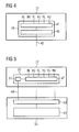
- FIG. 4 shows an inverter module 27 and its circuitry for receiving signals from and sending signals to the central controller 33 in a highly schematic view.
- the circuitry 39 comprises a decoder circuit 47 for distributing the switching states to the switching devices 35 according to a control message received from the central controller 33 via the serial data link 40.
- the control message is sent by the central controller 33 in threefold over the serial data link 40.
- a voting module 49 in the circuitry 39 (or, alternatively, connected to the circuitry 39) receives the threefold control message and runs a majority voting algorithm.
- the control message is then forwarded to the decoder circuit 47 if all three copies of the control message are identical.
- the bit contained in these two control messages is used in the version of the control message forwarded to the distribution circuit 47.
- the voting module may either set the inverter module 27 to a fault state, or may keep the previously set switching states until the next threefold control message arrives.
- all three copies of the control message differ from each other the inverter module 27 is set to a fault state. Otherwise, the switching states contained in this control message are distributed to the active switching devices 35 so that the operation of the inverter module 27 can continue.
- the converter is able to carry on running even in the event of a single message error.
- the respective inverter module receiving the single message error will be in a incorrect state for 2 ⁇ s time period, which results in a small amount of waveform distortion, the system and the appliance connected thereto can be laid out so that such a waveform distortion is tolerable.
- FIG. 5 A second alternative which allows the inverter to carry on running in case of a message error is shown in Figure 5 .
- the Figure shows an inverter module 27 with its circuitry 33 which contains the decoder circuit 47 described with respect to Figure 4 and a CRC-check module 51.
- the central controller comprises a CRC-code generator 53 that generates, for each control message, a check sum and adds the check sum to the control message before sending it to an inverter module 27 via the serial data link 40.
- the CRC-check module recalculates the CRC-code and, in case the CRC-code is found to be identical with the received code, forwards the control message to the decoder circuit 47.
- the control message is not forwarded to the decoder circuit 47, and either the inverter module 27 is set to a fault state or, preferably, the active switching devices are kept in the states they have been set according to the previously received control message.
- the next control message is received and the CRC-code calculated by the CRC-check module 51 is identical with the received CRC-code this control message is forwarded to the decoder circuit 47, and the respective switching states are distributed to the active switching devices 35.
- the CRC-code of said following message calculated by the CRC-check module 51 differs from the received CRC-code the inverter module 27 is set to a fault state.
- a message error may be detected and, if possible, corrected by a majority voting algorithm or detected by a CRC-check-algorithm.
- the system can just be kept in the previously set switching states so that it might be in an incorrect state until the next timing cycle.
- If two consecutive control messages contain errors the respective inverter module is set to a fault state. Note, however, that it is not mandatory to set the inverter module to a fault state if two consecutive control messages contain errors. If the inverter module and the appliance controlled by the converter module tolerate incorrect switch states for more than one timing cycle an inverter module may be set to fault state only when more than two consecutive control messages contain errors.
- control message contains an error in its timing data
- these errors can be handled by the inclusion of additional logic at the receiving circuitry, which ensures the immediate requirements of the converter bridges are satisfied, for example that the dead times and minimum on/of times are respected.
- the communication links interconnecting the central controller 33 and the inverter modules 27_1, 27_2, 27_3 are full-duplex links. This means that, at the same time data is transmitted from the central controller 33 to the inverter modules 27_1, 27_2, 27_3, data can be transmitted from the inverter modules 27_1, 27_2, 27_3 to the central controller 33.
- data transmitted from the inverter modules to the central controller may include voltage feedbacks, current feedbacks, intervention signals, for example a disable signal in the event of an overcurrent, etc. In this way, a coordinated shut down of the parallel or series connected inverter modules can be achieved, using the single cable communication system without the need for extra dedicated communication lines.
- each converter module of a power converter is connected to a central controller only by a serial cable, like a copper cable or an optical cable, control messages can be sent to the converter modules which fulfil the following requirements:
Landscapes
- Engineering & Computer Science (AREA)
- Power Engineering (AREA)
- Inverter Devices (AREA)
- Power Conversion In General (AREA)
- Supply And Distribution Of Alternating Current (AREA)
Priority Applications (8)
| Application Number | Priority Date | Filing Date | Title |
|---|---|---|---|
| DK10000316.9T DK2346155T3 (da) | 2010-01-14 | 2010-01-14 | Fremgangsmåde og styresystem til at styre effektomformning i en effektomformer |
| ES10000316.9T ES2519165T3 (es) | 2010-01-14 | 2010-01-14 | Método y sistema de control para controlar la conversión de potencia en un convertidor de potencia |
| EP10000316.9A EP2346155B1 (de) | 2010-01-14 | 2010-01-14 | Verfahren und Steuerungssystem zur Steuerung der Leistungswandlung in einem Leistungswandler |
| US12/987,203 US8050067B2 (en) | 2010-01-14 | 2011-01-10 | Method and control system for controlling power conversion in a power converter |
| NZ590403A NZ590403A (en) | 2010-01-14 | 2011-01-10 | Method and control system for controlling power conversion in a power converter |
| CA2727683A CA2727683C (en) | 2010-01-14 | 2011-01-12 | Method and control system for controlling power conversion in a power converter |
| JP2011006398A JP5850620B2 (ja) | 2010-01-14 | 2011-01-14 | 電力コンバータの電力変換を制御するための方法およびコントロールシステム |
| CN201110007425.1A CN102130620B (zh) | 2010-01-14 | 2011-01-14 | 用于控制功率变换器中的功率变换的方法和控制系统 |
Applications Claiming Priority (1)
| Application Number | Priority Date | Filing Date | Title |
|---|---|---|---|
| EP10000316.9A EP2346155B1 (de) | 2010-01-14 | 2010-01-14 | Verfahren und Steuerungssystem zur Steuerung der Leistungswandlung in einem Leistungswandler |
Publications (2)
| Publication Number | Publication Date |
|---|---|
| EP2346155A1 true EP2346155A1 (de) | 2011-07-20 |
| EP2346155B1 EP2346155B1 (de) | 2014-08-27 |
Family
ID=42194762
Family Applications (1)
| Application Number | Title | Priority Date | Filing Date |
|---|---|---|---|
| EP10000316.9A Active EP2346155B1 (de) | 2010-01-14 | 2010-01-14 | Verfahren und Steuerungssystem zur Steuerung der Leistungswandlung in einem Leistungswandler |
Country Status (8)
| Country | Link |
|---|---|
| US (1) | US8050067B2 (de) |
| EP (1) | EP2346155B1 (de) |
| JP (1) | JP5850620B2 (de) |
| CN (1) | CN102130620B (de) |
| CA (1) | CA2727683C (de) |
| DK (1) | DK2346155T3 (de) |
| ES (1) | ES2519165T3 (de) |
| NZ (1) | NZ590403A (de) |
Cited By (5)
| Publication number | Priority date | Publication date | Assignee | Title |
|---|---|---|---|---|
| WO2013102779A1 (en) * | 2012-01-05 | 2013-07-11 | American Power Conversion Corporation | Methods and apparatus for controlling power switches via a digital communication bus |
| DE102013212012A1 (de) * | 2013-06-25 | 2015-01-08 | Bayerische Motoren Werke Aktiengesellschaft | Mehr-Ebenen-Parallel Umrichter Kaskade |
| EP2595304A3 (de) * | 2011-11-18 | 2016-07-27 | Eaton Corporation | Leistungssystem, das Leistungs-Halbleitervorrichtungen steuert und überwacht, welches zwei serielle Signale verwendet |
| US9670907B2 (en) | 2011-03-30 | 2017-06-06 | Vestas Wind Systems A/S | Wind turbine control system with decentralized voting |
| EP2795795B1 (de) * | 2011-12-23 | 2019-06-12 | Maschinenfabrik Reinhausen GmbH | Steuersystem für fehlertolerante leistungshalbleiterschaltung |
Families Citing this family (25)
| Publication number | Priority date | Publication date | Assignee | Title |
|---|---|---|---|---|
| CA2709758C (en) * | 2008-01-08 | 2016-05-10 | Abb Technology Ag | A method for controlling a voltage source converter and a voltage converting apparatus |
| ES2398174B1 (es) * | 2010-09-09 | 2014-01-27 | Gamesa Innovation & Technology S.L. | Sistema de control de un convertidor. |
| GB201114868D0 (en) * | 2011-08-30 | 2011-10-12 | Rolls Royce Plc | Method of controlling an inverter and a controller for controlling an inverter |
| KR101792040B1 (ko) * | 2011-11-25 | 2017-11-02 | 엘에스산전 주식회사 | 병렬 인버터 시스템 |
| GB2497969B (en) * | 2011-12-23 | 2018-08-29 | Reinhausen Maschf Scheubeck | Switching control system signalling techniques |
| GB2497968A (en) * | 2011-12-23 | 2013-07-03 | Amantys Ltd | Switching very large numbers of power semiconductor devices in synchronisation |
| CN102780385B (zh) * | 2012-07-27 | 2016-08-03 | 华为技术有限公司 | 一种级联变换器的控制方法和相关设备 |
| US8984197B2 (en) * | 2012-12-11 | 2015-03-17 | Agileswitch, Llc | Power stack control systems |
| KR20150119029A (ko) * | 2013-02-11 | 2015-10-23 | 에이비비 테크놀로지 아게 | 병렬 스위치를 위한 구동 신호의 장애 검출 |
| EP2793392B1 (de) * | 2013-04-16 | 2023-07-12 | Siemens Aktiengesellschaft | Steuergerät zur Steuerung eines Stromwandlers |
| KR101491933B1 (ko) * | 2013-11-19 | 2015-02-09 | 엘에스산전 주식회사 | 병렬 인버터 제어 장치 |
| KR101562117B1 (ko) | 2014-01-23 | 2015-10-22 | 엘에스산전 주식회사 | 초고압 직류송전 시스템의 제어 장치 및 방법 |
| KR101622458B1 (ko) | 2014-05-07 | 2016-05-18 | 엘에스산전 주식회사 | Hvdc 시스템의 컨버터 장치 및 그의 제어 방법 |
| JP6192054B2 (ja) * | 2014-05-14 | 2017-09-06 | 東芝三菱電機産業システム株式会社 | 電力変換装置、ゲート駆動回路および電力変換装置の異常検出方法 |
| KR101950302B1 (ko) * | 2014-07-23 | 2019-02-20 | 엘에스산전 주식회사 | 고압 인버터의 병렬 운전 방법 |
| US9960707B2 (en) | 2014-08-29 | 2018-05-01 | Enphase Energy, Inc. | Parallel power converter |
| EP3070807B1 (de) * | 2015-03-19 | 2020-09-09 | General Electric Technology GmbH | Leistungsübertragungsnetzwerk |
| KR101641460B1 (ko) | 2015-03-23 | 2016-07-20 | 엘에스산전 주식회사 | 고전압 직류 송전 시스템의 데이터 처리 장치 및 방법 |
| CN105509346B (zh) * | 2015-12-28 | 2017-11-03 | 中海阳能源集团股份有限公司 | 一种塔式定日镜的偏差校正系统及其校正方法 |
| CN109642918B (zh) * | 2016-08-24 | 2021-03-09 | 东芝三菱电机产业系统株式会社 | 脉冲宽度调制转换器用输入滤波器的上电评价试验装置 |
| US11251706B2 (en) * | 2019-05-15 | 2022-02-15 | Texas Instruments Incorporated | Multiphase switched mode power supply clocking circuits and related methods |
| DE102019208122A1 (de) * | 2019-06-04 | 2020-12-10 | Audi Ag | Verfahren zum Betrieb einer elektrischen Schaltung, elektrische Schaltung und Kraftfahrzeug |
| CN113970906A (zh) * | 2020-07-22 | 2022-01-25 | 台达电子企业管理(上海)有限公司 | 多单元协作分布式的电气控制系统及电气系统 |
| US20220026859A1 (en) * | 2021-07-16 | 2022-01-27 | Delta Electronics (Shanghai) Co., Ltd. | Multi-unit cooperative distributed electrical control system and electrical system |
| CN114413749B (zh) * | 2022-03-31 | 2022-06-10 | 苏州纳芯微电子股份有限公司 | 磁场感测装置及磁场感测方法 |
Citations (4)
| Publication number | Priority date | Publication date | Assignee | Title |
|---|---|---|---|---|
| US6389041B1 (en) * | 1997-12-05 | 2002-05-14 | Hitachi, Ltd. | Synchronization system and synchronization method of multisystem control apparatus |
| JP2005333246A (ja) * | 2004-05-18 | 2005-12-02 | Fuji Electric Systems Co Ltd | 光伝送装置及び電力変換装置 |
| US20060022656A1 (en) * | 2004-07-27 | 2006-02-02 | Kafai Leung | Digital PWM controller for digital power supply having programmable dead times |
| WO2009087063A1 (en) | 2008-01-08 | 2009-07-16 | Abb Technology Ag | Power converter with distributed cell control |
Family Cites Families (11)
| Publication number | Priority date | Publication date | Assignee | Title |
|---|---|---|---|---|
| US638904A (en) * | 1898-04-18 | 1899-12-12 | William De Pons | Device for making cigarettes. |
| JPH0315263A (ja) * | 1989-06-12 | 1991-01-23 | Fuji Electric Co Ltd | 半導体電力変換装置の制御装置 |
| FR2752111B1 (fr) * | 1996-07-30 | 1998-10-30 | Texas Instruments France | Procede et dispositif de commande d'onduleurs |
| JP3570476B2 (ja) * | 1998-01-26 | 2004-09-29 | 富士電機システムズ株式会社 | 電力変換装置 |
| JP2004266723A (ja) * | 2003-03-04 | 2004-09-24 | Matsushita Electric Ind Co Ltd | ネットワークシステム、データ送受信装置、およびデータ送受信方法 |
| JP4579591B2 (ja) * | 2004-06-25 | 2010-11-10 | 東芝三菱電機産業システム株式会社 | 電力変換装置 |
| US7502240B2 (en) * | 2004-07-27 | 2009-03-10 | Silicon Laboratories Inc. | Distributed power supply system with separate SYNC control for controlling remote digital DC/DC converters |
| SE527687C2 (sv) * | 2004-08-31 | 2006-05-09 | Abb Technology Ltd | Anordning och metod för styrning av en spänningsstyv strömriktare |
| JP4509134B2 (ja) * | 2007-04-16 | 2010-07-21 | 株式会社日立製作所 | 電力変換装置とその制御方法 |
| CA2714211C (en) * | 2008-02-13 | 2015-06-30 | Masaki Kono | Electrical power conversion apparatus |
| CN101409518B (zh) * | 2008-11-12 | 2011-07-20 | 国电南京自动化股份有限公司 | 基于igct的二电平特定消谐脉宽调制实现方法 |
-
2010
- 2010-01-14 ES ES10000316.9T patent/ES2519165T3/es active Active
- 2010-01-14 DK DK10000316.9T patent/DK2346155T3/da active
- 2010-01-14 EP EP10000316.9A patent/EP2346155B1/de active Active
-
2011
- 2011-01-10 NZ NZ590403A patent/NZ590403A/xx unknown
- 2011-01-10 US US12/987,203 patent/US8050067B2/en active Active
- 2011-01-12 CA CA2727683A patent/CA2727683C/en active Active
- 2011-01-14 CN CN201110007425.1A patent/CN102130620B/zh active Active
- 2011-01-14 JP JP2011006398A patent/JP5850620B2/ja active Active
Patent Citations (4)
| Publication number | Priority date | Publication date | Assignee | Title |
|---|---|---|---|---|
| US6389041B1 (en) * | 1997-12-05 | 2002-05-14 | Hitachi, Ltd. | Synchronization system and synchronization method of multisystem control apparatus |
| JP2005333246A (ja) * | 2004-05-18 | 2005-12-02 | Fuji Electric Systems Co Ltd | 光伝送装置及び電力変換装置 |
| US20060022656A1 (en) * | 2004-07-27 | 2006-02-02 | Kafai Leung | Digital PWM controller for digital power supply having programmable dead times |
| WO2009087063A1 (en) | 2008-01-08 | 2009-07-16 | Abb Technology Ag | Power converter with distributed cell control |
Cited By (6)
| Publication number | Priority date | Publication date | Assignee | Title |
|---|---|---|---|---|
| US9670907B2 (en) | 2011-03-30 | 2017-06-06 | Vestas Wind Systems A/S | Wind turbine control system with decentralized voting |
| EP2595304A3 (de) * | 2011-11-18 | 2016-07-27 | Eaton Corporation | Leistungssystem, das Leistungs-Halbleitervorrichtungen steuert und überwacht, welches zwei serielle Signale verwendet |
| EP2795795B1 (de) * | 2011-12-23 | 2019-06-12 | Maschinenfabrik Reinhausen GmbH | Steuersystem für fehlertolerante leistungshalbleiterschaltung |
| WO2013102779A1 (en) * | 2012-01-05 | 2013-07-11 | American Power Conversion Corporation | Methods and apparatus for controlling power switches via a digital communication bus |
| US9490689B2 (en) | 2012-01-05 | 2016-11-08 | Schneider Electric It Corporation | Methods and apparatus for controlling power switches via a digital communication bus |
| DE102013212012A1 (de) * | 2013-06-25 | 2015-01-08 | Bayerische Motoren Werke Aktiengesellschaft | Mehr-Ebenen-Parallel Umrichter Kaskade |
Also Published As
| Publication number | Publication date |
|---|---|
| CN102130620A (zh) | 2011-07-20 |
| US8050067B2 (en) | 2011-11-01 |
| ES2519165T3 (es) | 2014-11-06 |
| US20110170323A1 (en) | 2011-07-14 |
| CA2727683A1 (en) | 2011-07-14 |
| JP5850620B2 (ja) | 2016-02-03 |
| JP2011147334A (ja) | 2011-07-28 |
| DK2346155T3 (da) | 2014-10-27 |
| NZ590403A (en) | 2012-08-31 |
| CN102130620B (zh) | 2015-06-17 |
| EP2346155B1 (de) | 2014-08-27 |
| CA2727683C (en) | 2018-10-16 |
Similar Documents
| Publication | Publication Date | Title |
|---|---|---|
| EP2346155B1 (de) | Verfahren und Steuerungssystem zur Steuerung der Leistungswandlung in einem Leistungswandler | |
| Friedrich | Modern HVDC PLUS application of VSC in modular multilevel converter topology | |
| US7939959B2 (en) | Wind turbine with parallel converters utilizing a plurality of isolated transformer windings | |
| EP2497187B1 (de) | Steuersystem für windparks mit windgeneratoren mit modularen gleichstromwandlern | |
| EP2372862A2 (de) | Gleichstromübertragungssystem für Fernsolarfarmen | |
| EP2628238B1 (de) | Anordnung zur leistungsübertragung zwischen einer gleichspannungsleitung und einer wechselspannungsleitung | |
| CN106337782A (zh) | 用网络桥接器控制器来运行风力涡轮机 | |
| EP3306635B1 (de) | Gleichstromschutzschalter | |
| CN105322530A (zh) | 用于将电力发电机连接到hvdc传输系统的装置和方法 | |
| CN111971885A (zh) | 具有有源滤波器的dfig转换器 | |
| EP3117500B1 (de) | Verfahren und vorrichtung zur erzeugung von strom mit offshore-windturbinen | |
| AU2015244410A1 (en) | Multi-module dc-to-dc power transformation system | |
| US20180219501A1 (en) | Control Method for Power Converters with Inverter Blocks with Silicon Carbide Mosfets | |
| US20150036395A1 (en) | Internal inverter communications | |
| Jin et al. | Communication-based distributed control of the stacked polyphase bridges converter | |
| US10284080B2 (en) | Column-switched multi-module DC-to-DC power transformation system | |
| CN104584360A (zh) | 用于检测电机的孤岛并且保护电机的系统和方法 | |
| CN219436892U (zh) | 变流器制动单元、变流器及风力发电机组 | |
| KR101390312B1 (ko) | H―브릿지 컨버터 시스템 | |
| WO2023248300A1 (ja) | 電力変換装置およびその制御方法 | |
| US20240171072A1 (en) | Dc/dc converter device for a wind turbine, an electric drive system, or an industrial dc supply network and operating method | |
| Eni | Fault tolerant distributed control strategy for modular multilevel converter in HVDC applications | |
| CN113809930A (zh) | 一种dc-dc变换器及其控制策略 | |
| CN106337779A (zh) | 用网络桥接器控制器来操作风力涡轮机 | |
| CN111108290A (zh) | 混合功率生成系统和其相关联的方法 |
Legal Events
| Date | Code | Title | Description |
|---|---|---|---|
| PUAI | Public reference made under article 153(3) epc to a published international application that has entered the european phase |
Free format text: ORIGINAL CODE: 0009012 |
|
| AK | Designated contracting states |
Kind code of ref document: A1 Designated state(s): AT BE BG CH CY CZ DE DK EE ES FI FR GB GR HR HU IE IS IT LI LT LU LV MC MK MT NL NO PL PT RO SE SI SK SM TR |
|
| AX | Request for extension of the european patent |
Extension state: AL BA RS |
|
| 17P | Request for examination filed |
Effective date: 20110808 |
|
| RAP1 | Party data changed (applicant data changed or rights of an application transferred) |
Owner name: SIEMENS AKTIENGESELLSCHAFT |
|
| REG | Reference to a national code |
Ref country code: DE Ref legal event code: R079 Ref document number: 602010018494 Country of ref document: DE Free format text: PREVIOUS MAIN CLASS: H02M0007493000 Ipc: H02M0007538700 |
|
| RIC1 | Information provided on ipc code assigned before grant |
Ipc: H02J 3/38 20060101ALI20131204BHEP Ipc: H04L 1/00 20060101ALI20131204BHEP Ipc: H02M 7/5387 20070101AFI20131204BHEP |
|
| GRAP | Despatch of communication of intention to grant a patent |
Free format text: ORIGINAL CODE: EPIDOSNIGR1 |
|
| INTG | Intention to grant announced |
Effective date: 20140117 |
|
| RIN1 | Information on inventor provided before grant (corrected) |
Inventor name: JONES, RODNEY Inventor name: FULCHER, ROBERT VERNON Inventor name: WAITE, PHILIP PERRY |
|
| GRAS | Grant fee paid |
Free format text: ORIGINAL CODE: EPIDOSNIGR3 |
|
| GRAP | Despatch of communication of intention to grant a patent |
Free format text: ORIGINAL CODE: EPIDOSNIGR1 |
|
| INTG | Intention to grant announced |
Effective date: 20140528 |
|
| GRAA | (expected) grant |
Free format text: ORIGINAL CODE: 0009210 |
|
| AK | Designated contracting states |
Kind code of ref document: B1 Designated state(s): AT BE BG CH CY CZ DE DK EE ES FI FR GB GR HR HU IE IS IT LI LT LU LV MC MK MT NL NO PL PT RO SE SI SK SM TR |
|
| REG | Reference to a national code |
Ref country code: GB Ref legal event code: FG4D |
|
| REG | Reference to a national code |
Ref country code: CH Ref legal event code: EP |
|
| REG | Reference to a national code |
Ref country code: AT Ref legal event code: REF Ref document number: 684925 Country of ref document: AT Kind code of ref document: T Effective date: 20140915 |
|
| GRAF | Information related to payment of grant fee modified |
Free format text: ORIGINAL CODE: EPIDOSCIGR3 |
|
| REG | Reference to a national code |
Ref country code: IE Ref legal event code: FG4D |
|
| REG | Reference to a national code |
Ref country code: DE Ref legal event code: R096 Ref document number: 602010018494 Country of ref document: DE Effective date: 20141009 |
|
| REG | Reference to a national code |
Ref country code: DK Ref legal event code: T3 Effective date: 20141022 |
|
| REG | Reference to a national code |
Ref country code: ES Ref legal event code: FG2A Ref document number: 2519165 Country of ref document: ES Kind code of ref document: T3 Effective date: 20141106 |
|
| REG | Reference to a national code |
Ref country code: AT Ref legal event code: MK05 Ref document number: 684925 Country of ref document: AT Kind code of ref document: T Effective date: 20140827 |
|
| REG | Reference to a national code |
Ref country code: LT Ref legal event code: MG4D |
|
| REG | Reference to a national code |
Ref country code: NL Ref legal event code: VDEP Effective date: 20140827 |
|
| PG25 | Lapsed in a contracting state [announced via postgrant information from national office to epo] |
Ref country code: FI Free format text: LAPSE BECAUSE OF FAILURE TO SUBMIT A TRANSLATION OF THE DESCRIPTION OR TO PAY THE FEE WITHIN THE PRESCRIBED TIME-LIMIT Effective date: 20140827 Ref country code: SE Free format text: LAPSE BECAUSE OF FAILURE TO SUBMIT A TRANSLATION OF THE DESCRIPTION OR TO PAY THE FEE WITHIN THE PRESCRIBED TIME-LIMIT Effective date: 20140827 Ref country code: BG Free format text: LAPSE BECAUSE OF FAILURE TO SUBMIT A TRANSLATION OF THE DESCRIPTION OR TO PAY THE FEE WITHIN THE PRESCRIBED TIME-LIMIT Effective date: 20141127 Ref country code: GR Free format text: LAPSE BECAUSE OF FAILURE TO SUBMIT A TRANSLATION OF THE DESCRIPTION OR TO PAY THE FEE WITHIN THE PRESCRIBED TIME-LIMIT Effective date: 20141128 Ref country code: LT Free format text: LAPSE BECAUSE OF FAILURE TO SUBMIT A TRANSLATION OF THE DESCRIPTION OR TO PAY THE FEE WITHIN THE PRESCRIBED TIME-LIMIT Effective date: 20140827 Ref country code: NO Free format text: LAPSE BECAUSE OF FAILURE TO SUBMIT A TRANSLATION OF THE DESCRIPTION OR TO PAY THE FEE WITHIN THE PRESCRIBED TIME-LIMIT Effective date: 20141127 Ref country code: PT Free format text: LAPSE BECAUSE OF FAILURE TO SUBMIT A TRANSLATION OF THE DESCRIPTION OR TO PAY THE FEE WITHIN THE PRESCRIBED TIME-LIMIT Effective date: 20141229 |
|
| PG25 | Lapsed in a contracting state [announced via postgrant information from national office to epo] |
Ref country code: CY Free format text: LAPSE BECAUSE OF FAILURE TO SUBMIT A TRANSLATION OF THE DESCRIPTION OR TO PAY THE FEE WITHIN THE PRESCRIBED TIME-LIMIT Effective date: 20140827 Ref country code: HR Free format text: LAPSE BECAUSE OF FAILURE TO SUBMIT A TRANSLATION OF THE DESCRIPTION OR TO PAY THE FEE WITHIN THE PRESCRIBED TIME-LIMIT Effective date: 20140827 Ref country code: LV Free format text: LAPSE BECAUSE OF FAILURE TO SUBMIT A TRANSLATION OF THE DESCRIPTION OR TO PAY THE FEE WITHIN THE PRESCRIBED TIME-LIMIT Effective date: 20140827 Ref country code: AT Free format text: LAPSE BECAUSE OF FAILURE TO SUBMIT A TRANSLATION OF THE DESCRIPTION OR TO PAY THE FEE WITHIN THE PRESCRIBED TIME-LIMIT Effective date: 20140827 Ref country code: IS Free format text: LAPSE BECAUSE OF FAILURE TO SUBMIT A TRANSLATION OF THE DESCRIPTION OR TO PAY THE FEE WITHIN THE PRESCRIBED TIME-LIMIT Effective date: 20141227 |
|
| PG25 | Lapsed in a contracting state [announced via postgrant information from national office to epo] |
Ref country code: NL Free format text: LAPSE BECAUSE OF FAILURE TO SUBMIT A TRANSLATION OF THE DESCRIPTION OR TO PAY THE FEE WITHIN THE PRESCRIBED TIME-LIMIT Effective date: 20140827 |
|
| PG25 | Lapsed in a contracting state [announced via postgrant information from national office to epo] |
Ref country code: RO Free format text: LAPSE BECAUSE OF FAILURE TO SUBMIT A TRANSLATION OF THE DESCRIPTION OR TO PAY THE FEE WITHIN THE PRESCRIBED TIME-LIMIT Effective date: 20140827 Ref country code: SK Free format text: LAPSE BECAUSE OF FAILURE TO SUBMIT A TRANSLATION OF THE DESCRIPTION OR TO PAY THE FEE WITHIN THE PRESCRIBED TIME-LIMIT Effective date: 20140827 Ref country code: IT Free format text: LAPSE BECAUSE OF FAILURE TO SUBMIT A TRANSLATION OF THE DESCRIPTION OR TO PAY THE FEE WITHIN THE PRESCRIBED TIME-LIMIT Effective date: 20140827 Ref country code: CZ Free format text: LAPSE BECAUSE OF FAILURE TO SUBMIT A TRANSLATION OF THE DESCRIPTION OR TO PAY THE FEE WITHIN THE PRESCRIBED TIME-LIMIT Effective date: 20140827 Ref country code: EE Free format text: LAPSE BECAUSE OF FAILURE TO SUBMIT A TRANSLATION OF THE DESCRIPTION OR TO PAY THE FEE WITHIN THE PRESCRIBED TIME-LIMIT Effective date: 20140827 |
|
| REG | Reference to a national code |
Ref country code: DE Ref legal event code: R097 Ref document number: 602010018494 Country of ref document: DE |
|
| PG25 | Lapsed in a contracting state [announced via postgrant information from national office to epo] |
Ref country code: PL Free format text: LAPSE BECAUSE OF FAILURE TO SUBMIT A TRANSLATION OF THE DESCRIPTION OR TO PAY THE FEE WITHIN THE PRESCRIBED TIME-LIMIT Effective date: 20140827 |
|
| PG25 | Lapsed in a contracting state [announced via postgrant information from national office to epo] |
Ref country code: BE Free format text: LAPSE BECAUSE OF NON-PAYMENT OF DUE FEES Effective date: 20150131 |
|
| PLBE | No opposition filed within time limit |
Free format text: ORIGINAL CODE: 0009261 |
|
| STAA | Information on the status of an ep patent application or granted ep patent |
Free format text: STATUS: NO OPPOSITION FILED WITHIN TIME LIMIT |
|
| 26N | No opposition filed |
Effective date: 20150528 |
|
| REG | Reference to a national code |
Ref country code: CH Ref legal event code: PL |
|
| PG25 | Lapsed in a contracting state [announced via postgrant information from national office to epo] |
Ref country code: LU Free format text: LAPSE BECAUSE OF FAILURE TO SUBMIT A TRANSLATION OF THE DESCRIPTION OR TO PAY THE FEE WITHIN THE PRESCRIBED TIME-LIMIT Effective date: 20150114 |
|
| PG25 | Lapsed in a contracting state [announced via postgrant information from national office to epo] |
Ref country code: MC Free format text: LAPSE BECAUSE OF FAILURE TO SUBMIT A TRANSLATION OF THE DESCRIPTION OR TO PAY THE FEE WITHIN THE PRESCRIBED TIME-LIMIT Effective date: 20140827 |
|
| PG25 | Lapsed in a contracting state [announced via postgrant information from national office to epo] |
Ref country code: CH Free format text: LAPSE BECAUSE OF NON-PAYMENT OF DUE FEES Effective date: 20150131 Ref country code: LI Free format text: LAPSE BECAUSE OF NON-PAYMENT OF DUE FEES Effective date: 20150131 |
|
| REG | Reference to a national code |
Ref country code: IE Ref legal event code: MM4A |
|
| PG25 | Lapsed in a contracting state [announced via postgrant information from national office to epo] |
Ref country code: SI Free format text: LAPSE BECAUSE OF FAILURE TO SUBMIT A TRANSLATION OF THE DESCRIPTION OR TO PAY THE FEE WITHIN THE PRESCRIBED TIME-LIMIT Effective date: 20140827 |
|
| REG | Reference to a national code |
Ref country code: FR Ref legal event code: PLFP Year of fee payment: 7 |
|
| PG25 | Lapsed in a contracting state [announced via postgrant information from national office to epo] |
Ref country code: IE Free format text: LAPSE BECAUSE OF NON-PAYMENT OF DUE FEES Effective date: 20150114 |
|
| PG25 | Lapsed in a contracting state [announced via postgrant information from national office to epo] |
Ref country code: BE Free format text: LAPSE BECAUSE OF FAILURE TO SUBMIT A TRANSLATION OF THE DESCRIPTION OR TO PAY THE FEE WITHIN THE PRESCRIBED TIME-LIMIT Effective date: 20140827 |
|
| PG25 | Lapsed in a contracting state [announced via postgrant information from national office to epo] |
Ref country code: MT Free format text: LAPSE BECAUSE OF FAILURE TO SUBMIT A TRANSLATION OF THE DESCRIPTION OR TO PAY THE FEE WITHIN THE PRESCRIBED TIME-LIMIT Effective date: 20140827 |
|
| REG | Reference to a national code |
Ref country code: FR Ref legal event code: PLFP Year of fee payment: 8 |
|
| PG25 | Lapsed in a contracting state [announced via postgrant information from national office to epo] |
Ref country code: HU Free format text: LAPSE BECAUSE OF FAILURE TO SUBMIT A TRANSLATION OF THE DESCRIPTION OR TO PAY THE FEE WITHIN THE PRESCRIBED TIME-LIMIT; INVALID AB INITIO Effective date: 20100114 Ref country code: SM Free format text: LAPSE BECAUSE OF FAILURE TO SUBMIT A TRANSLATION OF THE DESCRIPTION OR TO PAY THE FEE WITHIN THE PRESCRIBED TIME-LIMIT Effective date: 20140827 |
|
| PG25 | Lapsed in a contracting state [announced via postgrant information from national office to epo] |
Ref country code: TR Free format text: LAPSE BECAUSE OF FAILURE TO SUBMIT A TRANSLATION OF THE DESCRIPTION OR TO PAY THE FEE WITHIN THE PRESCRIBED TIME-LIMIT Effective date: 20140827 |
|
| REG | Reference to a national code |
Ref country code: FR Ref legal event code: PLFP Year of fee payment: 9 |
|
| PG25 | Lapsed in a contracting state [announced via postgrant information from national office to epo] |
Ref country code: MK Free format text: LAPSE BECAUSE OF FAILURE TO SUBMIT A TRANSLATION OF THE DESCRIPTION OR TO PAY THE FEE WITHIN THE PRESCRIBED TIME-LIMIT Effective date: 20140827 |
|
| REG | Reference to a national code |
Ref country code: ES Ref legal event code: PC2A Owner name: SIEMENS GAMESA RENEWABLE ENERGY A/S Effective date: 20210525 |
|
| REG | Reference to a national code |
Ref country code: GB Ref legal event code: 732E Free format text: REGISTERED BETWEEN 20210624 AND 20210630 |
|
| PGFP | Annual fee paid to national office [announced via postgrant information from national office to epo] |
Ref country code: FR Payment date: 20230123 Year of fee payment: 14 Ref country code: DK Payment date: 20230123 Year of fee payment: 14 |
|
| P01 | Opt-out of the competence of the unified patent court (upc) registered |
Effective date: 20230526 |
|
| REG | Reference to a national code |
Ref country code: DE Ref legal event code: R081 Ref document number: 602010018494 Country of ref document: DE Owner name: INNOMOTICS GMBH, DE Free format text: FORMER OWNER: SIEMENS AKTIENGESELLSCHAFT, 80333 MUENCHEN, DE |
|
| PGFP | Annual fee paid to national office [announced via postgrant information from national office to epo] |
Ref country code: ES Payment date: 20240216 Year of fee payment: 15 |
|
| PGFP | Annual fee paid to national office [announced via postgrant information from national office to epo] |
Ref country code: DE Payment date: 20240318 Year of fee payment: 15 Ref country code: GB Payment date: 20240124 Year of fee payment: 15 |