EP2346081A1 - Trench-gate vertical MOSFET manufacturing method - Google Patents
Trench-gate vertical MOSFET manufacturing method Download PDFInfo
- Publication number
- EP2346081A1 EP2346081A1 EP20110165247 EP11165247A EP2346081A1 EP 2346081 A1 EP2346081 A1 EP 2346081A1 EP 20110165247 EP20110165247 EP 20110165247 EP 11165247 A EP11165247 A EP 11165247A EP 2346081 A1 EP2346081 A1 EP 2346081A1
- Authority
- EP
- European Patent Office
- Prior art keywords
- mesa
- sidewalls
- forming
- dielectric regions
- trenches
- Prior art date
- Legal status (The legal status is an assumption and is not a legal conclusion. Google has not performed a legal analysis and makes no representation as to the accuracy of the status listed.)
- Granted
Links
Images


Classifications
-
- H—ELECTRICITY
- H10—SEMICONDUCTOR DEVICES; ELECTRIC SOLID-STATE DEVICES NOT OTHERWISE PROVIDED FOR
- H10D—INORGANIC ELECTRIC SEMICONDUCTOR DEVICES
- H10D30/00—Field-effect transistors [FET]
- H10D30/60—Insulated-gate field-effect transistors [IGFET]
- H10D30/64—Double-diffused metal-oxide semiconductor [DMOS] FETs
- H10D30/66—Vertical DMOS [VDMOS] FETs
- H10D30/668—Vertical DMOS [VDMOS] FETs having trench gate electrodes, e.g. UMOS transistors
-
- H—ELECTRICITY
- H10—SEMICONDUCTOR DEVICES; ELECTRIC SOLID-STATE DEVICES NOT OTHERWISE PROVIDED FOR
- H10D—INORGANIC ELECTRIC SEMICONDUCTOR DEVICES
- H10D30/00—Field-effect transistors [FET]
- H10D30/01—Manufacture or treatment
- H10D30/021—Manufacture or treatment of FETs having insulated gates [IGFET]
- H10D30/028—Manufacture or treatment of FETs having insulated gates [IGFET] of double-diffused metal oxide semiconductor [DMOS] FETs
- H10D30/0291—Manufacture or treatment of FETs having insulated gates [IGFET] of double-diffused metal oxide semiconductor [DMOS] FETs of vertical DMOS [VDMOS] FETs
- H10D30/0297—Manufacture or treatment of FETs having insulated gates [IGFET] of double-diffused metal oxide semiconductor [DMOS] FETs of vertical DMOS [VDMOS] FETs using recessing of the gate electrodes, e.g. to form trench gate electrodes
-
- H—ELECTRICITY
- H10—SEMICONDUCTOR DEVICES; ELECTRIC SOLID-STATE DEVICES NOT OTHERWISE PROVIDED FOR
- H10D—INORGANIC ELECTRIC SEMICONDUCTOR DEVICES
- H10D64/00—Electrodes of devices having potential barriers
- H10D64/111—Field plates
- H10D64/117—Recessed field plates, e.g. trench field plates or buried field plates
-
- H—ELECTRICITY
- H10—SEMICONDUCTOR DEVICES; ELECTRIC SOLID-STATE DEVICES NOT OTHERWISE PROVIDED FOR
- H10D—INORGANIC ELECTRIC SEMICONDUCTOR DEVICES
- H10D64/00—Electrodes of devices having potential barriers
- H10D64/20—Electrodes characterised by their shapes, relative sizes or dispositions
- H10D64/23—Electrodes carrying the current to be rectified, amplified, oscillated or switched, e.g. sources, drains, anodes or cathodes
- H10D64/251—Source or drain electrodes for field-effect devices
- H10D64/252—Source or drain electrodes for field-effect devices for vertical or pseudo-vertical devices
-
- H—ELECTRICITY
- H10—SEMICONDUCTOR DEVICES; ELECTRIC SOLID-STATE DEVICES NOT OTHERWISE PROVIDED FOR
- H10P—GENERIC PROCESSES OR APPARATUS FOR THE MANUFACTURE OR TREATMENT OF DEVICES COVERED BY CLASS H10
- H10P50/00—Etching of wafers, substrates or parts of devices
- H10P50/20—Dry etching; Plasma etching; Reactive-ion etching
- H10P50/28—Dry etching; Plasma etching; Reactive-ion etching of insulating materials
Definitions
- the present disclosure relates to semiconductor processes for fabricating high-voltage, field-effect transistors.
- High-voltage, field-effect transistors are well known in the semiconductor arts. Many HVFETs employ a device structure that includes an extended drain region that supports or blocks the applied high-voltage (e.g., several hundred volts) when the device is in the "off' state.
- a mesa of semiconductor material forms the extended drain or drift region for current flow in the on-state.
- a trench gate structure is formed near the top of the substrate, adjacent the sidewall regions of the mesa where the body region is disposed.
- a conductive channel to be formed along the vertical sidewall portion of the body region such that current may flow vertically through the semiconductor material, i.e., from a top surface of the substrate where the source region is disposed, down to the bottom of the substrate where the drain region is located.
- Figure 1A illustrates an example cross-sectional side view of a vertical HVFET in a fabrication process after the initial step of forming an epitaxial layer on a substrate.
- Figure 1B illustrates the example device structure of Figure 1A following vertical trench etching that forms a silicon mesa.
- Figure 1C illustrates the example device structure of Figure 1B after formation of a dielectric layer on the sidewalls of the mesa and filling of the remaining portions of the trenches with polysilicon.
- Figure 1D illustrates the example device structure of Figure 1C after masking of a top surface of the silicon substrate.
- Figure 1E illustrates the example device structure of Figure 1D after formation of the gate trenches.
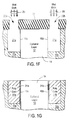
- Figure 1F illustrates the example device structure of Figure 1E following removal of the oxide covering the sidewalls of the mesa in the gate trenches.
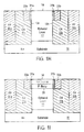
- Figure 1G illustrates the example device structure of Figure 1F after removal of the masking layer, formation of a thin gate oxide the sidewalls of the mesa, and subsequent filling of the gate trenches.
- Figure 1H illustrates the example device structure of Figure 1G in an expanded view that shows the field plates in relation to the trench gate structure.
- Figure 1I illustrates the example device structure of Figure 1H after formation of the source and body regions.
- Figure 1 illustrates an example cross-sectional side view of a vertical HVFET in a fabrication process after the initial step of forming an epitaxial layer 12 of N-type semiconductor material on an N+ doped silicon substrate 11.
- epitaxial layer 12 has a vertical thickness in a range about 15 ⁇ m to 120 ⁇ m thick.
- the N+ substrate 11 is heavily doped to minimize its resistance to current flowing through to the drain electrode, which is located on the bottom of the substrate in the completed device.
- Doping of epitaxial layer 12 may be carried out as the layer is being formed.
- the doping concentration of epitaxial layer 12 is linearly graded to produce an extended drain region that exhibits a substantially uniform electric-field distribution. Linear grading may stop at some point below the top surface of the epitaxial layer 12.
- FIG. 1B illustrates an example cross-sectional side view of a vertical HVFET in a fabrication process following vertical trench etching that forms a silicon mesa 14.
- the height and width of mesa 14, as well as the spacing between adjacent vertical trenches may be determined by the breakdown voltage requirements of the device.
- Mesa 14 of epitaxial material 12 eventually forms the N-type drift region of the final HVFET device structure. It should be understood that mesa 14, in various embodiments, may extend a considerable lateral distance in an orthogonal direction (into and out of the page).
- the lateral width of the N-type drift region formed by mesa 14 is as narrow as can be reliably manufactured in order to achieve a very high breakdown voltage (e.g., 600V).
- Figure 1C illustrates the example device structure of Figure 1B after formation of a dielectric layer, on the sidewalls of mesa 14 to form oxide regions 15, and subsequent filling of the remaining portions of the trenches with polysilicon or another suitable material to form field plates 35a & 35b.
- the dielectric layer preferably comprises silicon dioxide, though silicon nitride or other suitable dielectric materials may also be used.
- oxide region 15a covers sidewall 19a of mesa 14, while oxide region 15b covers sidewall 19b on the opposite side of mesa 14.
- Sidewall oxide regions 15a & 15b also cover the exposed portion of N+ substrate 11 in each of the respective trenches.
- Oxide regions 15 may be formed using a variety of well-known methods, including thermal growth and chemical vapor deposition.
- the remaining open portions of the trenches are filled with a conductive material that forms field plates 35a & 35b.
- the top surface of the substrate may then be planarized utilizing conventional techniques such as chemical-mechanical polishing.
- the conductive material used to from the field plates may comprise a heavily doped polysilicon, a metal (or metal alloys), a silicide, or other suitable materials.
- field plate members 35a & 35b normally function as capacitive plates that may be used to deplete the extended drain region of charge when the HVFET is in the off state (i.e., when the drain is raised to a high voltage potential).
- the lateral thickness of sidewall oxide 15 that separates each field plate 35 from sidewall 19 of mesa 14 is approximately 4 ⁇ m.
- Figure 1D illustrates the example device structure of Figure 1C after masking of a top surface of the silicon substrate.
- the masking layer 21 comprises a layer of photoresist having openings 22a and 22b over oxide regions 15a and 15b, respectively, on opposite sides of mesa 14.
- the portion of masking layer 21 directly above mesa 14 extends or overlaps a distance "d" beyond the edge of sidewall 19 over each side of the mesa to cover first and second sidewall portions of oxide regions 15a and 15b. That is, the edge of each opening 22 closest to mesa 14 is not coincident with sidewall 19 of mesa 14; rather, openings 22 are intentionally offset so that the nearest edge of each opening 22 is a small distance away from the corresponding mesa sidewall 19.
- the overlap distance "d" is approximately 0.2 ⁇ m to 0.5 ⁇ m.
- Figure 1E illustrates the example device structure of Figure 1D after formation of the gate trenches 24a and 24b.
- Gate trenches 24a and 24b are formed by a first dielectric etch (shown by arrows 26) that removes the dielectric material of oxide regions 15 in the areas directly below openings 22.
- the first dielectric etch is a plasma etch that is substantially anisotropic.
- First dielectric etch 26 is performed down to the desired or target depth, which is about 3 ⁇ m deep in one embodiment.
- a mixture of C 4 F 8 /CO/Ar/O 2 gases, for example, may be utilized for plasma etch 26.
- the anisotropic nature of the first etch produces a substantially vertical sidewall profile in the gate trench that does not extend or penetrate to the sidewalls 19 of mesa 14.
- the overlap distance "d" of masking layer 21 is such that anisotropic etching through openings 22 does not attack the silicon mesa sidewalls 19; instead, a portion of the dielectric material comprising oxide regions 15 still remains covering sidewalls 19 after the first dielectric etch.
- Figure 1F illustrates the example device structure of Figure 1E following removal of the oxide covering the sidewalls 19 of mesa 14 in the gate trenches.
- a second dielectric etch (shown by arrows 29) may be performed through openings 22a & 22b of masking layer 21 to completely remove the remaining oxide on sidewalls 19a and 19b.
- the second dielectric etch is a wet etch (e.g., using buffered HF) that is substantially isotropic in nature.
- the result is a pair of gate trench openings 27a and 27b that expose the epitaxial silicon material along sidewalls 19a & 19b, respectively, of mesa 14.
- the second dielectric etch 29 is highly selective, which means that it etches the dielectric material at a much faster rate than it etches silicon. Using this process, the silicon surface of each sidewall 19 is undamaged, thereby allowing a high-quality gate oxide to be subsequently grown on the sidewall surface.
- the gate trench is etched at a similar rate in both the vertical and lateral directions.
- the second dielectric etch is utilized to remove the remaining few tenths of a micron of silicon dioxide on the silicon mesa sidewall, the overall effect on the aspect ratio of trench gate openings 27 is relatively insignificant.
- the lateral width of each gate trench opening 27 is approximately 1.5 ⁇ m wide, and the final depth is approximately 3.5 ⁇ m.
- Figure 1G illustrates the example device structure of Figure 1F after removal of the masking layer 21, formation of a high-quality, thin (e.g., ⁇ 500 ⁇ ) gate oxide layer 31, which covers the exposed portions of sidewalls 19, and subsequent filling of the gate trenches.
- gate oxide layer 31 is thermally grown with a thickness in the range of 100 to 1000 ⁇ .
- Masking layer 21 is removed prior to formation of gate oxide 31.
- the remaining portion of each gate trench is filled with doped polysilicon or another suitable material, which form gate members 33a & 33b in the completed device structure.
- Figure 1H illustrates the example device structure of Figure 1G in an expanded view that shows field plates 35a & 35b in relation to the trench gate structure.
- the trench gate structure includes gate members 33 disposed adjacent to, and insulated from, sidewalls 19 of mesa 14 by gate oxide layer 31.
- the overlap distance "d" of masking layer 21 should be sufficiently large enough such that even under a worst-case mask misalignment error scenario, the resulting overlap of masking layer 21 with respect to the sidewall of mesa 14 still prevents plasma etch 26 from attacking the silicon material along either one of sidewalls 19.
- the masking distance "d" of masking layer 21 should not be so large such that in a worst-case mask misalignment scenario the oxide remaining on either one of sidewalls 19 cannot be removed by a reasonable second dielectric etch.
- the second dielectric etch 29 needed to remove the oxide covering sidewalls 19 might result in excessive thinning of the oxide remaining between (i.e., separating) gate members 33 and field plates 35, potentially leading to inadequate isolation between these elements.
- Figure 1I illustrates the example device structure of Figure 1H after formation of N+ source region 38 and P-type body region 39 near the top of epitaxial layer 12.
- Source region 38 and body region 39 may each be formed using ordinary deposition, diffusion, and/or implantation processing techniques.
- the HVFET may be completed by forming source, drain, gate, and field plate electrodes that electrically connect to the respective regions / materials of the device using conventional fabrication methods (not shown in the figures for clarity reasons).
Landscapes
- Electrodes Of Semiconductors (AREA)
- Thin Film Transistor (AREA)
- Drying Of Semiconductors (AREA)
- Element Separation (AREA)
- Junction Field-Effect Transistors (AREA)
- Insulated Gate Type Field-Effect Transistor (AREA)
Abstract
Description
- The present disclosure relates to semiconductor processes for fabricating high-voltage, field-effect transistors.
- High-voltage, field-effect transistors (HVFETs) are well known in the semiconductor arts. Many HVFETs employ a device structure that includes an extended drain region that supports or blocks the applied high-voltage (e.g., several hundred volts) when the device is in the "off' state. In a conventional vertical HVFET structure, a mesa of semiconductor material forms the extended drain or drift region for current flow in the on-state. A trench gate structure is formed near the top of the substrate, adjacent the sidewall regions of the mesa where the body region is disposed. Application of an appropriate voltage potential to the gate causes a conductive channel to be formed along the vertical sidewall portion of the body region such that current may flow vertically through the semiconductor material, i.e., from a top surface of the substrate where the source region is disposed, down to the bottom of the substrate where the drain region is located.
- The present invention is illustrated by way of example, and not limitation, in the figures of the accompanying drawings, wherein:
-
Figure 1A illustrates an example cross-sectional side view of a vertical HVFET in a fabrication process after the initial step of forming an epitaxial layer on a substrate. -
Figure 1B illustrates the example device structure ofFigure 1A following vertical trench etching that forms a silicon mesa. -
Figure 1C illustrates the example device structure ofFigure 1B after formation of a dielectric layer on the sidewalls of the mesa and filling of the remaining portions of the trenches with polysilicon. -
Figure 1D illustrates the example device structure ofFigure 1C after masking of a top surface of the silicon substrate. -
Figure 1E illustrates the example device structure ofFigure 1D after formation of the gate trenches. -
Figure 1F illustrates the example device structure ofFigure 1E following removal of the oxide covering the sidewalls of the mesa in the gate trenches. -
Figure 1G illustrates the example device structure ofFigure 1F after removal of the masking layer, formation of a thin gate oxide the sidewalls of the mesa, and subsequent filling of the gate trenches. -
Figure 1H illustrates the example device structure ofFigure 1G in an expanded view that shows the field plates in relation to the trench gate structure. -
Figure 1I illustrates the example device structure ofFigure 1H after formation of the source and body regions. - In the following description specific details are set forth, such as material types, dimensions, structural features, processing steps, etc., in order to provide a thorough understanding of the present invention. However, persons having ordinary skill in the relevant arts will appreciate that these specific details may not be needed to practice the present invention.
- It should be understood that the elements in the figures are representational, and are not drawn to scale in the interest of clarity. It is also appreciated that although a method for fabricating an N-channel HVFET device is disclosed, a P-channel HVFET may also be fabricated by utilizing the opposite conductivity types for all of the illustrated doped regions. Furthermore, although the figures appear to show a single device, those of skill will understand that such transistor structures are commonly fabricated in a repeated, inter-digitated, or otherwise replicated manner. In other words, the method for fabricating a vertical HVFET device structure shown by way of the various example processing steps in
Figures 1A-1I may be utilized to construct a device having plurality of parallel-arranged or replicated regions. -
Figure 1 illustrates an example cross-sectional side view of a vertical HVFET in a fabrication process after the initial step of forming anepitaxial layer 12 of N-type semiconductor material on an N+ dopedsilicon substrate 11. In one embodiment,epitaxial layer 12 has a vertical thickness in a range about 15µm to 120µm thick. TheN+ substrate 11 is heavily doped to minimize its resistance to current flowing through to the drain electrode, which is located on the bottom of the substrate in the completed device. Doping ofepitaxial layer 12 may be carried out as the layer is being formed. In one embodiment, the doping concentration ofepitaxial layer 12 is linearly graded to produce an extended drain region that exhibits a substantially uniform electric-field distribution. Linear grading may stop at some point below the top surface of theepitaxial layer 12. - After
epitaxial layer 12 has been formed, the top surface of the semiconductor wafer is appropriately masked and deep vertical trenches are then etched intoepitaxial layer 12.Figure 1B illustrates an example cross-sectional side view of a vertical HVFET in a fabrication process following vertical trench etching that forms asilicon mesa 14. The height and width ofmesa 14, as well as the spacing between adjacent vertical trenches may be determined by the breakdown voltage requirements of the device.Mesa 14 ofepitaxial material 12 eventually forms the N-type drift region of the final HVFET device structure. It should be understood thatmesa 14, in various embodiments, may extend a considerable lateral distance in an orthogonal direction (into and out of the page). In certain embodiments, the lateral width of the N-type drift region formed bymesa 14 is as narrow as can be reliably manufactured in order to achieve a very high breakdown voltage (e.g., 600V). -
Figure 1C illustrates the example device structure ofFigure 1B after formation of a dielectric layer, on the sidewalls ofmesa 14 to form oxide regions 15, and subsequent filling of the remaining portions of the trenches with polysilicon or another suitable material to formfield plates 35a & 35b. The dielectric layer preferably comprises silicon dioxide, though silicon nitride or other suitable dielectric materials may also be used. In this example,oxide region 15a coverssidewall 19a ofmesa 14, whileoxide region 15b coverssidewall 19b on the opposite side ofmesa 14.Sidewall oxide regions 15a & 15b also cover the exposed portion ofN+ substrate 11 in each of the respective trenches. Oxide regions 15 may be formed using a variety of well-known methods, including thermal growth and chemical vapor deposition. - Following the formation of sidewall oxide regions 15, the remaining open portions of the trenches are filled with a conductive material that forms
field plates 35a & 35b. The top surface of the substrate may then be planarized utilizing conventional techniques such as chemical-mechanical polishing. The conductive material used to from the field plates may comprise a heavily doped polysilicon, a metal (or metal alloys), a silicide, or other suitable materials. In the completed device structure,field plate members 35a & 35b normally function as capacitive plates that may be used to deplete the extended drain region of charge when the HVFET is in the off state (i.e., when the drain is raised to a high voltage potential). In one embodiment, the lateral thickness of sidewall oxide 15 that separates each field plate 35 from sidewall 19 ofmesa 14 is approximately 4µm. -
Figure 1D illustrates the example device structure ofFigure 1C after masking of a top surface of the silicon substrate. In this example, themasking layer 21 comprises a layer ofphotoresist having openings oxide regions mesa 14. Note that the portion ofmasking layer 21 directly abovemesa 14 extends or overlaps a distance "d" beyond the edge of sidewall 19 over each side of the mesa to cover first and second sidewall portions ofoxide regions mesa 14 is not coincident with sidewall 19 ofmesa 14; rather, openings 22 are intentionally offset so that the nearest edge of each opening 22 is a small distance away from the corresponding mesa sidewall 19. In one embodiment, the overlap distance "d" is approximately 0.2µm to 0.5µm. -
Figure 1E illustrates the example device structure ofFigure 1D after formation of thegate trenches Gate trenches dielectric etch 26 is performed down to the desired or target depth, which is about 3µm deep in one embodiment. A mixture of C4F8/CO/Ar/O2 gases, for example, may be utilized forplasma etch 26. Note that the anisotropic nature of the first etch produces a substantially vertical sidewall profile in the gate trench that does not extend or penetrate to the sidewalls 19 ofmesa 14. Stated differently, the overlap distance "d" ofmasking layer 21 is such that anisotropic etching through openings 22 does not attack the silicon mesa sidewalls 19; instead, a portion of the dielectric material comprising oxide regions 15 still remains covering sidewalls 19 after the first dielectric etch. -
Figure 1F illustrates the example device structure ofFigure 1E following removal of the oxide covering the sidewalls 19 ofmesa 14 in the gate trenches. A second dielectric etch (shown by arrows 29) may performed throughopenings 22a & 22b ofmasking layer 21 to completely remove the remaining oxide onsidewalls gate trench openings sidewalls 19a & 19b, respectively, ofmesa 14. - In the embodiment shown, the second
dielectric etch 29 is highly selective, which means that it etches the dielectric material at a much faster rate than it etches silicon. Using this process, the silicon surface of each sidewall 19 is undamaged, thereby allowing a high-quality gate oxide to be subsequently grown on the sidewall surface. In addition, due to the substantially isotropic nature of the second dielectric etch, the gate trench is etched at a similar rate in both the vertical and lateral directions. However, as the second dielectric etch is utilized to remove the remaining few tenths of a micron of silicon dioxide on the silicon mesa sidewall, the overall effect on the aspect ratio of trench gate openings 27 is relatively insignificant. In one embodiment, the lateral width of each gate trench opening 27 is approximately 1.5µm wide, and the final depth is approximately 3.5µm. -
Figure 1G illustrates the example device structure ofFigure 1F after removal of themasking layer 21, formation of a high-quality, thin (e.g., ∼500Å) gate oxide layer 31, which covers the exposed portions of sidewalls 19, and subsequent filling of the gate trenches. ln one embodiment, gate oxide layer 31 is thermally grown with a thickness in the range of 100 to 1000Å. Maskinglayer 21 is removed prior to formation of gate oxide 31. The remaining portion of each gate trench is filled with doped polysilicon or another suitable material, which formgate members 33a & 33b in the completed device structure. -
Figure 1H illustrates the example device structure ofFigure 1G in an expanded view that showsfield plates 35a & 35b in relation to the trench gate structure. The trench gate structure includes gate members 33 disposed adjacent to, and insulated from, sidewalls 19 ofmesa 14 by gate oxide layer 31. - Practitioners in the art will appreciate that the overlap distance "d" of masking
layer 21 should be sufficiently large enough such that even under a worst-case mask misalignment error scenario, the resulting overlap of maskinglayer 21 with respect to the sidewall ofmesa 14 still preventsplasma etch 26 from attacking the silicon material along either one of sidewalls 19. Similarly, the masking distance "d" of maskinglayer 21 should not be so large such that in a worst-case mask misalignment scenario the oxide remaining on either one of sidewalls 19 cannot be removed by a reasonable second dielectric etch. If, for example, the overlap distance "d" happens to be too large, thesecond dielectric etch 29 needed to remove the oxide covering sidewalls 19 might result in excessive thinning of the oxide remaining between (i.e., separating) gate members 33 and field plates 35, potentially leading to inadequate isolation between these elements. -
Figure 1I illustrates the example device structure ofFigure 1H after formation ofN+ source region 38 and P-type body region 39 near the top ofepitaxial layer 12.Source region 38 andbody region 39 may each be formed using ordinary deposition, diffusion, and/or implantation processing techniques. After formation of theN+ source region 38, the HVFET may be completed by forming source, drain, gate, and field plate electrodes that electrically connect to the respective regions / materials of the device using conventional fabrication methods (not shown in the figures for clarity reasons). - Although the present invention has been described in conjunction with specific embodiments, those of ordinary skill in the arts will appreciate that numerous modifications and alterations are well within the scope of the present invention. Accordingly, the specification and drawings are to be regarded in an illustrative rather than a restrictive sense.
- Although the present invention is defined in the attached claims, it should be understood that the present invention can also (alternatively) be defined in accordance with the following embodiments:
- 1. A method comprising:
- masking a semiconductor substrate with a masking layer that includes first and second openings respectively disposed over first and second dielectric regions located on opposite sides of a mesa of semiconductor material, the mesa having first and second sidewalls that respectively adjoin the first and second dielectric regions, the masking layer having a portion between the first and second openings that covers the mesa, the portion extending past the first and second sidewalls to cover first and second sidewall portions of the first and second dielectric regions, respectively;
- anisotropically etching the first and second dielectric regions through the respective first and second openings to create first and second trenches;
- removing the first and second sidewall portions of the first and second dielectric regions; and
- forming a gate oxide on the first and second sidewalls of the mesa.
- 2. The method of embodiment 1 wherein removing the first and second sidewall portions comprises isotropically etching the first and second dielectric regions in the first and second trenches.
- 3. The method of embodiment 2 wherein isotropically etching is performed using an etchant that is selective with respect to the semiconductor material such that the semiconductor material of the first and second sidewalls is undamaged.
- 4. The method of embodiment 1 further comprising, after forming the gate oxide, filling the first and second trenches with polysilicon.
- 5. The method of embodiment 1 further comprising forming first and second field plates that extend vertically down into the first and second dielectric regions on the opposite sides of the mesa.
- 6. The method of embodiment 5 wherein the first and second trenches are respectively disposed between the first and second field plates and the mesa.
- 7. A method comprising:
- plasma etching first and second dielectric regions through first and second openings of a mask layer to create first and second trenches, the first and second dielectric regions being located on opposite sides of a mesa of semiconductor material, the mesa having first and second sidewalls that respectively adjoin the first and second dielectric regions;
- wet etching the first and second dielectric regions in the first and second trenches to expose the first and second sidewalls; and
- forming a gate oxide on the first and second sidewalls of the mesa.
- 8. The method of embodiment 7 wherein plasma etching comprises an anisotropic etch.
- 9. The method of embodiment 7 wherein the mask layer includes a portion between the first and second openings that covers the mesa, the portion extending past the first and second sidewalls to cover first and second sidewall portions of the first and second dielectric regions, respectively.
- 10. The method of embodiment 7 wherein wet etching comprises an isotropic etch.
- 11. The method of embodiment 7 further comprising, after forming the gate oxide, forming first and second gate members in the first and second trenches.
- 12. The method of embodiment 7 further comprising forming first and second field plates that extend vertically down into the first and second dielectric regions on the opposite sides of the mesa.
- 13. The method of
embodiment 12 wherein the first and second trenches are respectively disposed between the first and second field plates and the mesa. - 14. A method, comprising:
- forming an epitaxial layer on a substrate, the epitaxial layer being of a first conductivity type and having a top surface;
- etching the epitaxial layer to form first and second trenches that define a mesa having first and second sidewalls;
- forming first and second dielectric regions in the first and second trenches, respectively, the first and second dielectric regions respectively covering the first and second sidewalls;
- forming first and second field plate members insulated from the mesa by the first and second dielectric regions, respectively;
- forming, in a masking layer, first and second openings respectively disposed over the first and second dielectric regions on opposite sides of the mesa, the masking layer having a portion between the first and second openings that covers the mesa, the portion overlapping the first and second sidewalls to cover first and second sidewall portions of the first and second dielectric regions, respectively;
- anisotropically etching the first and second dielectric regions through the respective first and second openings to create first and second gate trenches; and
- isotropically etching the first and second dielectric regions in the first and second gate trenches to remove the first and second sidewall portions.
- 15. The method of
embodiment 14 further comprising forming a gate oxide on each of the first and second sidewalls of the mesa. - 16. The method of embodiment 15 further comprising forming first and second gate members respectively insulated from the first and second sidewalls by the gate oxide.
- 17. The method of embodiment 16 further comprising forming a body region near a top surface of the mesa adjacent the gate members, the body region being of a second conductivity type.
- 18. The method of embodiment 17 further comprising forming a source region of the first conductivity type at the top surface of the mesa, the source region being disposed above the body region.
- 19. The method of embodiment 15 wherein forming the gate oxide comprises thermally growing the gate oxide.
- 20. The method of
embodiment 14 wherein the portion overlapping the first and second sidewalls extends past each of the first and second sidewall portions by an overlap distance. - 21. The method of embodiment 20 wherein the overlap distance is greater than a worst-case misalignment error between the masking layer and the mesa.
- 22. The method of embodiment 20 wherein the overlap distance is in a range of approximately 0.2 µm to 0.5 µm wide.
- 23. A method comprising:
- plasma etching first and second oxide regions through first and second openings of a mask layer to create first and second trenches located on opposite sides of a mesa of a semiconductor material, the plasma etching leaving an oxide layer covering each of first and second sidewalls of the mesa;
- etching the first and second oxide regions in the first and second trenches with an etchant to remove the oxide layer, the etchant being selective with respect to the semiconductor material such that the semiconductor material of the first and second sidewalls is undamaged; and
- thermally growing a gate oxide on the first and second sidewalls of the mesa.
- 24. The method of embodiment 23 wherein plasma etching comprises an anisotropic etch.
- 25. The method of embodiment 23 wherein the mask layer includes a portion between the first and second openings that covers the mesa, the portion extending past the first and second sidewalls to cover a portion of each of the first and second oxide regions.
- 26. A method comprising:
- etching, with a first etchant, first and second dielectric regions through first and second openings of a mask layer to create first and second trenches respectively disposed adjacent first and second sidewalls of a mesa of semiconductor material, leaving first and second portions of the first and second dielectric regions respectively covering the first and second sidewalls of the mesa, the mesa eventually comprising an extended drain region of a field-effect transistor; and
- etching, with a second etchant, the first and second portions to expose the first and second sidewalls.
- 27. The method of
embodiment 26 wherein the second etchant is selective with respect to the semiconductor material such that the semiconductor material of the first and second sidewalls is undamaged by the etching. - 28. The method of
embodiment 26 wherein the first etchant is substantially anisotropic and the second etchant is substantially isotropic. - 29. The method of
embodiment 26 wherein the etching by the second etchant is performed through the first and second openings of the mask layer.
Claims (15)
- A method comprising:masking a semiconductor substrate (11) with a masking layer (21) that includes first and second openings (22) respectively disposed over first and second dielectric regions (15) located on opposite sides of a mesa (14) of semiconductor material, the mesa (14) having first and second sidewalls (19) that respectively adjoin the first and second dielectric regions (15), the masking layer (21) having a portion between the first and second openings (22) that covers the mesa (14), the portion extending past the first and second sidewalls (19) to cover first and second sidewall portions of the first and second dielectric regions (15), respectively;anisotropically etching the first and second dielectric regions (15) through the respective first and second openings (22) to create first and second trenches;removing the first and second sidewall portions of the first and second dielectric regions (15); andforming a gate oxide on the first and second sidewalls (19) of the mesa (14).
- The method of claim 1 wherein removing the first and second sidewall portions comprises isotropically etching the first and second dielectric regions (15) in the first and second trenches.
- The method of claim 2 wherein isotropically etching is performed using an etchant that is selective with respect to the semiconductor material such that the semiconductor material of the first and second sidewalls (19) is undamaged.
- The method of any preceding claim further comprising, after forming the gate oxide, filling the first and second trenches with polysilicon.
- The method of claim 1 further comprising forming first and second field plates that extend vertically down into the first and second dielectric regions (15) on the opposite sides of the mesa (14).
- The method of claim 5 wherein the first and second trenches are respectively disposed between the first and second field plates and the mesa (14).
- The method of claim 1, 2, 5, or 6, wherein:anisotropically etching the first and second dielectric regions (15) comprises plasma etching the first and second dielectric regions (15); andremoving the first and second sidewall portions comprises wet etching the first and second dielectric regions (15) in the first and second trenches to expose the first and second sidewalls (19).
- The method of claim 7 further comprising, after forming the gate oxide, forming first and second gate members in the first and second trenches.
- The method of claim 1, further comprising:forming an epitaxial layer on the substrate (11), the epitaxial layer being of a first conductivity type and having a top surface;etching the epitaxial layer to form first and second trenches that define the mesa (14) having the first and second sidewalls (19);forming the first and second dielectric regions (15) in the first and second trenches, respectively, the first and second dielectric regions (15) respectively covering the first and second sidewalls (19);forming first and second field plate members insulated from the mesa (14) by the first and second dielectric regions (15), respectively;forming, in the masking layer (21), the first and second openings (22) ; andisotropically etching the first and second dielectric regions (15) in the first and second gate trenches to remove the first and second sidewall portions.
- The method of claim 9 further comprising forming first and second gate members respectively insulated from the first and second sidewalls (19) by the gate oxide.
- The method of claim 10 further comprising forming a body region near a top surface of the mesa (14) adjacent the gate members, the body region being of a second conductivity type.
- The method of claim 11 further comprising forming a source region of the first conductivity type at the top surface of the mesa (14), the source region being disposed above the body region.
- The method of claim 9 wherein forming the gate oxide comprises thermally growing the gate oxide.
- The method of claim 9 wherein the portion overlapping the first and second sidewalls (19) extends past each of the first and second sidewall portions by an overlap distance that is greater than a worst-case misalignment error between the masking layer (21) and the mesa (14), for example, in a range of approximately 0.2 µm to 0.5 µm wide.
- The method of claim 1, wherein:anisotropically etching the first and second dielectric regions (15) comprises plasma etching first and second oxide regions through the first and second openings (22), the plasma etching leaving an oxide layer covering each of first and second sidewalls (19) of the mesa (14);removing the first and second sidewall portions comprises etching the first and second oxide regions in the first and second trenches with an etchant to remove the oxide layer, the etchant being selective with respect to the semiconductor material such that the semiconductor material of the first and second sidewalls (19) is undamaged; andforming the gate oxide comprises thermally growing a gate oxide on the first and second sidewalls (19) of the mesa (14).
Applications Claiming Priority (2)
| Application Number | Priority Date | Filing Date | Title |
|---|---|---|---|
| US11/542,083 US7381618B2 (en) | 2006-10-03 | 2006-10-03 | Gate etch process for a high-voltage FET |
| EP07253213A EP1909331B1 (en) | 2006-10-03 | 2007-08-15 | Trench-gate vertical MOSFET manufacturing method |
Related Parent Applications (2)
| Application Number | Title | Priority Date | Filing Date |
|---|---|---|---|
| EP07253213A Division EP1909331B1 (en) | 2006-10-03 | 2007-08-15 | Trench-gate vertical MOSFET manufacturing method |
| EP07253213.8 Division | 2007-08-15 |
Related Child Applications (1)
| Application Number | Title | Priority Date | Filing Date |
|---|---|---|---|
| EP12192268 Division-Into | 2012-11-12 |
Publications (2)
| Publication Number | Publication Date |
|---|---|
| EP2346081A1 true EP2346081A1 (en) | 2011-07-20 |
| EP2346081B1 EP2346081B1 (en) | 2015-10-07 |
Family
ID=38814315
Family Applications (2)
| Application Number | Title | Priority Date | Filing Date |
|---|---|---|---|
| EP11165247.5A Not-in-force EP2346081B1 (en) | 2006-10-03 | 2007-08-15 | Trench-gate vertical MOSFET manufacturing method |
| EP07253213A Not-in-force EP1909331B1 (en) | 2006-10-03 | 2007-08-15 | Trench-gate vertical MOSFET manufacturing method |
Family Applications After (1)
| Application Number | Title | Priority Date | Filing Date |
|---|---|---|---|
| EP07253213A Not-in-force EP1909331B1 (en) | 2006-10-03 | 2007-08-15 | Trench-gate vertical MOSFET manufacturing method |
Country Status (5)
| Country | Link |
|---|---|
| US (2) | US7381618B2 (en) |
| EP (2) | EP2346081B1 (en) |
| JP (2) | JP4898619B2 (en) |
| CN (2) | CN101159233B (en) |
| AT (1) | ATE509374T1 (en) |
Families Citing this family (38)
| Publication number | Priority date | Publication date | Assignee | Title |
|---|---|---|---|---|
| US6573558B2 (en) * | 2001-09-07 | 2003-06-03 | Power Integrations, Inc. | High-voltage vertical transistor with a multi-layered extended drain structure |
| US7786533B2 (en) * | 2001-09-07 | 2010-08-31 | Power Integrations, Inc. | High-voltage vertical transistor with edge termination structure |
| US6635544B2 (en) * | 2001-09-07 | 2003-10-21 | Power Intergrations, Inc. | Method of fabricating a high-voltage transistor with a multi-layered extended drain structure |
| US7135748B2 (en) * | 2004-10-26 | 2006-11-14 | Power Integrations, Inc. | Integrated circuit with multi-length output transistor segment |
| US8093621B2 (en) | 2008-12-23 | 2012-01-10 | Power Integrations, Inc. | VTS insulated gate bipolar transistor |
| US7557406B2 (en) * | 2007-02-16 | 2009-07-07 | Power Integrations, Inc. | Segmented pillar layout for a high-voltage vertical transistor |
| US7859037B2 (en) * | 2007-02-16 | 2010-12-28 | Power Integrations, Inc. | Checkerboarded high-voltage vertical transistor layout |
| US8653583B2 (en) | 2007-02-16 | 2014-02-18 | Power Integrations, Inc. | Sensing FET integrated with a high-voltage transistor |
| US7875962B2 (en) * | 2007-10-15 | 2011-01-25 | Power Integrations, Inc. | Package for a power semiconductor device |
| US7964912B2 (en) | 2008-09-18 | 2011-06-21 | Power Integrations, Inc. | High-voltage vertical transistor with a varied width silicon pillar |
| CN101740376B (en) * | 2008-11-25 | 2012-06-13 | 中芯国际集成电路制造(北京)有限公司 | Method for regulating width of spacer wall and method for etching in construction of spacer wall |
| US7871882B2 (en) * | 2008-12-20 | 2011-01-18 | Power Integrations, Inc. | Method of fabricating a deep trench insulated gate bipolar transistor |
| US20100155831A1 (en) * | 2008-12-20 | 2010-06-24 | Power Integrations, Inc. | Deep trench insulated gate bipolar transistor |
| US8319278B1 (en) * | 2009-03-31 | 2012-11-27 | Maxpower Semiconductor, Inc. | Power device structures and methods using empty space zones |
| JP5583933B2 (en) * | 2009-07-28 | 2014-09-03 | 猛英 白土 | Semiconductor device and manufacturing method thereof |
| US8207455B2 (en) * | 2009-07-31 | 2012-06-26 | Power Integrations, Inc. | Power semiconductor package with bottom surface protrusions |
| US8115457B2 (en) | 2009-07-31 | 2012-02-14 | Power Integrations, Inc. | Method and apparatus for implementing a power converter input terminal voltage discharge circuit |
| US8207577B2 (en) * | 2009-09-29 | 2012-06-26 | Power Integrations, Inc. | High-voltage transistor structure with reduced gate capacitance |
| US7893754B1 (en) | 2009-10-02 | 2011-02-22 | Power Integrations, Inc. | Temperature independent reference circuit |
| US8634218B2 (en) * | 2009-10-06 | 2014-01-21 | Power Integrations, Inc. | Monolithic AC/DC converter for generating DC supply voltage |
| US8310845B2 (en) * | 2010-02-10 | 2012-11-13 | Power Integrations, Inc. | Power supply circuit with a control terminal for different functional modes of operation |
| CN102412249B (en) * | 2011-10-13 | 2014-10-08 | 上海华虹宏力半导体制造有限公司 | Power device structure capable of decreasing latch-up effect and fabrication method thereof |
| US8653600B2 (en) | 2012-06-01 | 2014-02-18 | Power Integrations, Inc. | High-voltage monolithic schottky device structure |
| CN104241341A (en) * | 2012-07-27 | 2014-12-24 | 俞国庆 | High-frequency low-power dissipation power MOS field-effect tube device |
| JP5802636B2 (en) * | 2012-09-18 | 2015-10-28 | 株式会社東芝 | Semiconductor device and manufacturing method thereof |
| US9455621B2 (en) | 2013-08-28 | 2016-09-27 | Power Integrations, Inc. | Controller IC with zero-crossing detector and capacitor discharge switching element |
| US9543396B2 (en) | 2013-12-13 | 2017-01-10 | Power Integrations, Inc. | Vertical transistor device structure with cylindrically-shaped regions |
| US10325988B2 (en) | 2013-12-13 | 2019-06-18 | Power Integrations, Inc. | Vertical transistor device structure with cylindrically-shaped field plates |
| US9362338B2 (en) | 2014-03-03 | 2016-06-07 | Sandisk Technologies Inc. | Vertical thin film transistors in non-volatile storage systems |
| DE112016000050B4 (en) * | 2015-04-17 | 2021-11-25 | Su Zhou Oriental Semiconductor Co., Ltd. | Method for manufacturing a split gate power device |
| US9667154B2 (en) | 2015-09-18 | 2017-05-30 | Power Integrations, Inc. | Demand-controlled, low standby power linear shunt regulator |
| US9602009B1 (en) | 2015-12-08 | 2017-03-21 | Power Integrations, Inc. | Low voltage, closed loop controlled energy storage circuit |
| US9629218B1 (en) | 2015-12-28 | 2017-04-18 | Power Integrations, Inc. | Thermal protection for LED bleeder in fault condition |
| EP3440696B1 (en) | 2016-04-08 | 2021-06-09 | Power Integrations, Inc. | Integrated resistor for semiconductor device |
| US10498300B2 (en) | 2017-07-17 | 2019-12-03 | Power Integrations, Inc. | Voltage-to-current transconductance operational amplifier with adaptive biasing |
| CN107799600B (en) * | 2017-09-19 | 2020-05-01 | 西安电子科技大学 | Stepped high-K dielectric layer element longitudinal double-diffusion metal oxide semiconductor field effect transistor |
| CN107785433B (en) * | 2017-09-19 | 2020-05-01 | 西安电子科技大学 | A stepped high-K dielectric layer wide-bandgap semiconductor vertical double-diffused metal-oxide-semiconductor field effect transistor |
| EP4376091A1 (en) * | 2022-11-24 | 2024-05-29 | Nexperia B.V. | Mosfet formation |
Citations (3)
| Publication number | Priority date | Publication date | Assignee | Title |
|---|---|---|---|---|
| US20010049167A1 (en) * | 2000-06-05 | 2001-12-06 | Madson Gordon K. | Method of manufacturing a trench mosfet using selective growth epitaxy |
| US20050104121A1 (en) * | 2001-09-07 | 2005-05-19 | Power Integrations, Inc. | Method of fabricating a high-voltage transistor with an extended drain structure |
| WO2006004746A2 (en) * | 2004-06-25 | 2006-01-12 | International Rectifier Corporation | Mosgated power semiconductor device with source field electrode |
Family Cites Families (11)
| Publication number | Priority date | Publication date | Assignee | Title |
|---|---|---|---|---|
| JPH0831568B2 (en) * | 1989-03-27 | 1996-03-27 | 沖電気工業株式会社 | Method for manufacturing semiconductor memory device |
| US6593619B1 (en) * | 1999-06-03 | 2003-07-15 | General Semiconductor, Inc. | High voltage power MOSFET having low on-resistance |
| KR100338783B1 (en) * | 2000-10-28 | 2002-06-01 | Samsung Electronics Co Ltd | Semiconductor device having expanded effective width of active region and fabricating method thereof |
| JP3553904B2 (en) * | 2001-04-11 | 2004-08-11 | 日本電信電話株式会社 | Supercritical drying method |
| US6555873B2 (en) * | 2001-09-07 | 2003-04-29 | Power Integrations, Inc. | High-voltage lateral transistor with a multi-layered extended drain structure |
| US6797440B2 (en) * | 2002-08-06 | 2004-09-28 | Freescale Semiconductor, Inc. | Method of forming a rim phase shifting mask and using the rim phase shifting mask to form a semiconductor device |
| US20050285140A1 (en) * | 2004-06-23 | 2005-12-29 | Chih-Hsin Ko | Isolation structure for strained channel transistors |
| JP4500558B2 (en) * | 2004-02-09 | 2010-07-14 | トヨタ自動車株式会社 | Insulated gate type semiconductor device manufacturing method |
| KR100672723B1 (en) * | 2005-06-27 | 2007-01-22 | 동부일렉트로닉스 주식회사 | Manufacturing Method of Flash Memory Device |
| DE102005047058B4 (en) * | 2005-09-30 | 2009-09-24 | Qimonda Ag | Manufacturing method for a trench transistor and corresponding trench transistor |
| KR100755670B1 (en) * | 2006-04-03 | 2007-09-05 | 삼성전자주식회사 | Manufacturing Method of Semiconductor Device |
-
2006
- 2006-10-03 US US11/542,083 patent/US7381618B2/en active Active
-
2007
- 2007-08-15 EP EP11165247.5A patent/EP2346081B1/en not_active Not-in-force
- 2007-08-15 EP EP07253213A patent/EP1909331B1/en not_active Not-in-force
- 2007-08-15 AT AT07253213T patent/ATE509374T1/en not_active IP Right Cessation
- 2007-10-02 JP JP2007258532A patent/JP4898619B2/en not_active Expired - Fee Related
- 2007-10-08 CN CN2007101622308A patent/CN101159233B/en not_active Expired - Fee Related
- 2007-10-08 CN CN2011100308659A patent/CN102130015B/en not_active Expired - Fee Related
-
2008
- 2008-03-15 US US12/075,897 patent/US7494875B2/en not_active Expired - Fee Related
-
2011
- 2011-12-26 JP JP2011283023A patent/JP5505407B2/en not_active Expired - Fee Related
Patent Citations (3)
| Publication number | Priority date | Publication date | Assignee | Title |
|---|---|---|---|---|
| US20010049167A1 (en) * | 2000-06-05 | 2001-12-06 | Madson Gordon K. | Method of manufacturing a trench mosfet using selective growth epitaxy |
| US20050104121A1 (en) * | 2001-09-07 | 2005-05-19 | Power Integrations, Inc. | Method of fabricating a high-voltage transistor with an extended drain structure |
| WO2006004746A2 (en) * | 2004-06-25 | 2006-01-12 | International Rectifier Corporation | Mosgated power semiconductor device with source field electrode |
Also Published As
| Publication number | Publication date |
|---|---|
| US20080085603A1 (en) | 2008-04-10 |
| JP2012060189A (en) | 2012-03-22 |
| HK1116921A1 (en) | 2009-01-02 |
| JP2008091924A (en) | 2008-04-17 |
| CN102130015B (en) | 2013-03-20 |
| US7494875B2 (en) | 2009-02-24 |
| US20080160705A1 (en) | 2008-07-03 |
| EP1909331B1 (en) | 2011-05-11 |
| US7381618B2 (en) | 2008-06-03 |
| JP5505407B2 (en) | 2014-05-28 |
| ATE509374T1 (en) | 2011-05-15 |
| CN101159233B (en) | 2011-03-23 |
| CN102130015A (en) | 2011-07-20 |
| EP2346081B1 (en) | 2015-10-07 |
| EP1909331A2 (en) | 2008-04-09 |
| EP1909331A3 (en) | 2009-04-15 |
| JP4898619B2 (en) | 2012-03-21 |
| CN101159233A (en) | 2008-04-09 |
Similar Documents
| Publication | Publication Date | Title |
|---|---|---|
| EP1909331B1 (en) | Trench-gate vertical MOSFET manufacturing method | |
| US7989886B2 (en) | Alignment of trench for MOS | |
| US8247287B2 (en) | Method of fabricating a deep trench insulated gate bipolar transistor | |
| US20130153995A1 (en) | Semiconductor device and method for manufacturing the same | |
| EP1978562A2 (en) | Trench gate MOSFET and method of manufacturing the same | |
| US20120043624A1 (en) | Ultra-thin body transistor and method for manufcturing the same | |
| EP2200087A1 (en) | Deep trench insulated gate bipolar transistor | |
| US8017494B2 (en) | Termination trench structure for mosgated device and process for its manufacture | |
| US6391699B1 (en) | Method of manufacturing a trench MOSFET using selective growth epitaxy | |
| US10090205B2 (en) | Fin profile improvement for high performance transistor | |
| JP2004311547A (en) | Method of manufacturing vertical MOS transistor | |
| US9941416B2 (en) | MOS transistor and method of manufacturing the same | |
| US6977203B2 (en) | Method of forming narrow trenches in semiconductor substrates | |
| US8084813B2 (en) | Short gate high power MOSFET and method of manufacture | |
| HK1116921B (en) | Gate etch process for a high-voltage fet | |
| US20040002222A1 (en) | Low cost method of providing a semiconductor device having a high channel density |
Legal Events
| Date | Code | Title | Description |
|---|---|---|---|
| PUAI | Public reference made under article 153(3) epc to a published international application that has entered the european phase |
Free format text: ORIGINAL CODE: 0009012 |
|
| 17P | Request for examination filed |
Effective date: 20110509 |
|
| AC | Divisional application: reference to earlier application |
Ref document number: 1909331 Country of ref document: EP Kind code of ref document: P |
|
| AK | Designated contracting states |
Kind code of ref document: A1 Designated state(s): AT BE BG CH CY CZ DE DK EE ES FI FR GB GR HU IE IS IT LI LT LU LV MC MT NL PL PT RO SE SI SK TR |
|
| 17Q | First examination report despatched |
Effective date: 20110901 |
|
| RIC1 | Information provided on ipc code assigned before grant |
Ipc: H01L 21/311 20060101ALN20150129BHEP Ipc: H01L 29/78 20060101AFI20150129BHEP Ipc: H01L 29/40 20060101ALI20150129BHEP Ipc: H01L 29/423 20060101ALI20150129BHEP Ipc: H01L 21/336 20060101ALI20150129BHEP |
|
| GRAP | Despatch of communication of intention to grant a patent |
Free format text: ORIGINAL CODE: EPIDOSNIGR1 |
|
| RIC1 | Information provided on ipc code assigned before grant |
Ipc: H01L 21/311 20060101ALN20150317BHEP Ipc: H01L 29/78 20060101AFI20150317BHEP Ipc: H01L 29/40 20060101ALI20150317BHEP Ipc: H01L 21/336 20060101ALI20150317BHEP Ipc: H01L 29/423 20060101ALI20150317BHEP |
|
| INTG | Intention to grant announced |
Effective date: 20150407 |
|
| GRAS | Grant fee paid |
Free format text: ORIGINAL CODE: EPIDOSNIGR3 |
|
| GRAA | (expected) grant |
Free format text: ORIGINAL CODE: 0009210 |
|
| AC | Divisional application: reference to earlier application |
Ref document number: 1909331 Country of ref document: EP Kind code of ref document: P |
|
| AK | Designated contracting states |
Kind code of ref document: B1 Designated state(s): AT BE BG CH CY CZ DE DK EE ES FI FR GB GR HU IE IS IT LI LT LU LV MC MT NL PL PT RO SE SI SK TR |
|
| REG | Reference to a national code |
Ref country code: GB Ref legal event code: FG4D |
|
| REG | Reference to a national code |
Ref country code: AT Ref legal event code: REF Ref document number: 754203 Country of ref document: AT Kind code of ref document: T Effective date: 20151015 Ref country code: CH Ref legal event code: EP |
|
| REG | Reference to a national code |
Ref country code: IE Ref legal event code: FG4D |
|
| REG | Reference to a national code |
Ref country code: DE Ref legal event code: R096 Ref document number: 602007043450 Country of ref document: DE |
|
| REG | Reference to a national code |
Ref country code: NL Ref legal event code: MP Effective date: 20151007 |
|
| REG | Reference to a national code |
Ref country code: AT Ref legal event code: MK05 Ref document number: 754203 Country of ref document: AT Kind code of ref document: T Effective date: 20151007 |
|
| REG | Reference to a national code |
Ref country code: LT Ref legal event code: MG4D |
|
| PG25 | Lapsed in a contracting state [announced via postgrant information from national office to epo] |
Ref country code: IS Free format text: LAPSE BECAUSE OF FAILURE TO SUBMIT A TRANSLATION OF THE DESCRIPTION OR TO PAY THE FEE WITHIN THE PRESCRIBED TIME-LIMIT Effective date: 20160207 Ref country code: LT Free format text: LAPSE BECAUSE OF FAILURE TO SUBMIT A TRANSLATION OF THE DESCRIPTION OR TO PAY THE FEE WITHIN THE PRESCRIBED TIME-LIMIT Effective date: 20151007 Ref country code: ES Free format text: LAPSE BECAUSE OF FAILURE TO SUBMIT A TRANSLATION OF THE DESCRIPTION OR TO PAY THE FEE WITHIN THE PRESCRIBED TIME-LIMIT Effective date: 20151007 Ref country code: NL Free format text: LAPSE BECAUSE OF FAILURE TO SUBMIT A TRANSLATION OF THE DESCRIPTION OR TO PAY THE FEE WITHIN THE PRESCRIBED TIME-LIMIT Effective date: 20151007 |
|
| PG25 | Lapsed in a contracting state [announced via postgrant information from national office to epo] |
Ref country code: SE Free format text: LAPSE BECAUSE OF FAILURE TO SUBMIT A TRANSLATION OF THE DESCRIPTION OR TO PAY THE FEE WITHIN THE PRESCRIBED TIME-LIMIT Effective date: 20151007 Ref country code: PT Free format text: LAPSE BECAUSE OF FAILURE TO SUBMIT A TRANSLATION OF THE DESCRIPTION OR TO PAY THE FEE WITHIN THE PRESCRIBED TIME-LIMIT Effective date: 20160208 Ref country code: AT Free format text: LAPSE BECAUSE OF FAILURE TO SUBMIT A TRANSLATION OF THE DESCRIPTION OR TO PAY THE FEE WITHIN THE PRESCRIBED TIME-LIMIT Effective date: 20151007 Ref country code: PL Free format text: LAPSE BECAUSE OF FAILURE TO SUBMIT A TRANSLATION OF THE DESCRIPTION OR TO PAY THE FEE WITHIN THE PRESCRIBED TIME-LIMIT Effective date: 20151007 Ref country code: GR Free format text: LAPSE BECAUSE OF FAILURE TO SUBMIT A TRANSLATION OF THE DESCRIPTION OR TO PAY THE FEE WITHIN THE PRESCRIBED TIME-LIMIT Effective date: 20160108 Ref country code: FI Free format text: LAPSE BECAUSE OF FAILURE TO SUBMIT A TRANSLATION OF THE DESCRIPTION OR TO PAY THE FEE WITHIN THE PRESCRIBED TIME-LIMIT Effective date: 20151007 Ref country code: LV Free format text: LAPSE BECAUSE OF FAILURE TO SUBMIT A TRANSLATION OF THE DESCRIPTION OR TO PAY THE FEE WITHIN THE PRESCRIBED TIME-LIMIT Effective date: 20151007 |
|
| REG | Reference to a national code |
Ref country code: DE Ref legal event code: R097 Ref document number: 602007043450 Country of ref document: DE |
|
| PG25 | Lapsed in a contracting state [announced via postgrant information from national office to epo] |
Ref country code: CZ Free format text: LAPSE BECAUSE OF FAILURE TO SUBMIT A TRANSLATION OF THE DESCRIPTION OR TO PAY THE FEE WITHIN THE PRESCRIBED TIME-LIMIT Effective date: 20151007 |
|
| PLBE | No opposition filed within time limit |
Free format text: ORIGINAL CODE: 0009261 |
|
| STAA | Information on the status of an ep patent application or granted ep patent |
Free format text: STATUS: NO OPPOSITION FILED WITHIN TIME LIMIT |
|
| REG | Reference to a national code |
Ref country code: FR Ref legal event code: PLFP Year of fee payment: 10 |
|
| PG25 | Lapsed in a contracting state [announced via postgrant information from national office to epo] |
Ref country code: EE Free format text: LAPSE BECAUSE OF FAILURE TO SUBMIT A TRANSLATION OF THE DESCRIPTION OR TO PAY THE FEE WITHIN THE PRESCRIBED TIME-LIMIT Effective date: 20151007 Ref country code: DK Free format text: LAPSE BECAUSE OF FAILURE TO SUBMIT A TRANSLATION OF THE DESCRIPTION OR TO PAY THE FEE WITHIN THE PRESCRIBED TIME-LIMIT Effective date: 20151007 Ref country code: RO Free format text: LAPSE BECAUSE OF FAILURE TO SUBMIT A TRANSLATION OF THE DESCRIPTION OR TO PAY THE FEE WITHIN THE PRESCRIBED TIME-LIMIT Effective date: 20151007 Ref country code: SK Free format text: LAPSE BECAUSE OF FAILURE TO SUBMIT A TRANSLATION OF THE DESCRIPTION OR TO PAY THE FEE WITHIN THE PRESCRIBED TIME-LIMIT Effective date: 20151007 |
|
| 26N | No opposition filed |
Effective date: 20160708 |
|
| PGFP | Annual fee paid to national office [announced via postgrant information from national office to epo] |
Ref country code: IT Payment date: 20160824 Year of fee payment: 10 |
|
| PG25 | Lapsed in a contracting state [announced via postgrant information from national office to epo] |
Ref country code: SI Free format text: LAPSE BECAUSE OF FAILURE TO SUBMIT A TRANSLATION OF THE DESCRIPTION OR TO PAY THE FEE WITHIN THE PRESCRIBED TIME-LIMIT Effective date: 20151007 |
|
| PGFP | Annual fee paid to national office [announced via postgrant information from national office to epo] |
Ref country code: FR Payment date: 20160825 Year of fee payment: 10 |
|
| PG25 | Lapsed in a contracting state [announced via postgrant information from national office to epo] |
Ref country code: BE Free format text: LAPSE BECAUSE OF FAILURE TO SUBMIT A TRANSLATION OF THE DESCRIPTION OR TO PAY THE FEE WITHIN THE PRESCRIBED TIME-LIMIT Effective date: 20151007 |
|
| PG25 | Lapsed in a contracting state [announced via postgrant information from national office to epo] |
Ref country code: MC Free format text: LAPSE BECAUSE OF FAILURE TO SUBMIT A TRANSLATION OF THE DESCRIPTION OR TO PAY THE FEE WITHIN THE PRESCRIBED TIME-LIMIT Effective date: 20151007 |
|
| REG | Reference to a national code |
Ref country code: CH Ref legal event code: PL |
|
| GBPC | Gb: european patent ceased through non-payment of renewal fee |
Effective date: 20160815 |
|
| PG25 | Lapsed in a contracting state [announced via postgrant information from national office to epo] |
Ref country code: LI Free format text: LAPSE BECAUSE OF NON-PAYMENT OF DUE FEES Effective date: 20160831 Ref country code: CH Free format text: LAPSE BECAUSE OF NON-PAYMENT OF DUE FEES Effective date: 20160831 |
|
| REG | Reference to a national code |
Ref country code: IE Ref legal event code: MM4A |
|
| PG25 | Lapsed in a contracting state [announced via postgrant information from national office to epo] |
Ref country code: IE Free format text: LAPSE BECAUSE OF NON-PAYMENT OF DUE FEES Effective date: 20160815 Ref country code: GB Free format text: LAPSE BECAUSE OF NON-PAYMENT OF DUE FEES Effective date: 20160815 |
|
| PG25 | Lapsed in a contracting state [announced via postgrant information from national office to epo] |
Ref country code: LU Free format text: LAPSE BECAUSE OF NON-PAYMENT OF DUE FEES Effective date: 20160815 |
|
| REG | Reference to a national code |
Ref country code: FR Ref legal event code: ST Effective date: 20180430 |
|
| PG25 | Lapsed in a contracting state [announced via postgrant information from national office to epo] |
Ref country code: HU Free format text: LAPSE BECAUSE OF FAILURE TO SUBMIT A TRANSLATION OF THE DESCRIPTION OR TO PAY THE FEE WITHIN THE PRESCRIBED TIME-LIMIT; INVALID AB INITIO Effective date: 20070815 Ref country code: CY Free format text: LAPSE BECAUSE OF FAILURE TO SUBMIT A TRANSLATION OF THE DESCRIPTION OR TO PAY THE FEE WITHIN THE PRESCRIBED TIME-LIMIT Effective date: 20151007 |
|
| PG25 | Lapsed in a contracting state [announced via postgrant information from national office to epo] |
Ref country code: TR Free format text: LAPSE BECAUSE OF FAILURE TO SUBMIT A TRANSLATION OF THE DESCRIPTION OR TO PAY THE FEE WITHIN THE PRESCRIBED TIME-LIMIT Effective date: 20151007 Ref country code: MT Free format text: LAPSE BECAUSE OF NON-PAYMENT OF DUE FEES Effective date: 20160831 |
|
| PG25 | Lapsed in a contracting state [announced via postgrant information from national office to epo] |
Ref country code: BG Free format text: LAPSE BECAUSE OF FAILURE TO SUBMIT A TRANSLATION OF THE DESCRIPTION OR TO PAY THE FEE WITHIN THE PRESCRIBED TIME-LIMIT Effective date: 20151007 |
|
| PG25 | Lapsed in a contracting state [announced via postgrant information from national office to epo] |
Ref country code: IT Free format text: LAPSE BECAUSE OF NON-PAYMENT OF DUE FEES Effective date: 20170815 Ref country code: FR Free format text: LAPSE BECAUSE OF NON-PAYMENT OF DUE FEES Effective date: 20170831 |
|
| PGFP | Annual fee paid to national office [announced via postgrant information from national office to epo] |
Ref country code: DE Payment date: 20180829 Year of fee payment: 12 |
|
| REG | Reference to a national code |
Ref country code: DE Ref legal event code: R119 Ref document number: 602007043450 Country of ref document: DE |
|
| PG25 | Lapsed in a contracting state [announced via postgrant information from national office to epo] |
Ref country code: DE Free format text: LAPSE BECAUSE OF NON-PAYMENT OF DUE FEES Effective date: 20200303 |