EP2345840A2 - Connector terminal for lamps - Google Patents
Connector terminal for lamps Download PDFInfo
- Publication number
- EP2345840A2 EP2345840A2 EP11250052A EP11250052A EP2345840A2 EP 2345840 A2 EP2345840 A2 EP 2345840A2 EP 11250052 A EP11250052 A EP 11250052A EP 11250052 A EP11250052 A EP 11250052A EP 2345840 A2 EP2345840 A2 EP 2345840A2
- Authority
- EP
- European Patent Office
- Prior art keywords
- connector
- circuit board
- circuit
- housing
- lamp
- Prior art date
- Legal status (The legal status is an assumption and is not a legal conclusion. Google has not performed a legal analysis and makes no representation as to the accuracy of the status listed.)
- Granted
Links
- 238000007789 sealing Methods 0.000 claims description 20
- 238000000034 method Methods 0.000 claims description 15
- NFLLKCVHYJRNRH-UHFFFAOYSA-N 8-chloro-1,3-dimethyl-7H-purine-2,6-dione 2-(diphenylmethyl)oxy-N,N-dimethylethanamine Chemical compound O=C1N(C)C(=O)N(C)C2=C1NC(Cl)=N2.C=1C=CC=CC=1C(OCCN(C)C)C1=CC=CC=C1 NFLLKCVHYJRNRH-UHFFFAOYSA-N 0.000 claims description 10
- 230000008878 coupling Effects 0.000 claims description 10
- 238000010168 coupling process Methods 0.000 claims description 10
- 238000005859 coupling reaction Methods 0.000 claims description 10
- 239000004033 plastic Substances 0.000 claims description 6
- 229920003023 plastic Polymers 0.000 claims description 6
- 238000005476 soldering Methods 0.000 claims description 5
- 238000003466 welding Methods 0.000 claims description 4
- 230000001419 dependent effect Effects 0.000 claims 3
- 239000000463 material Substances 0.000 description 4
- 230000006835 compression Effects 0.000 description 2
- 238000007906 compression Methods 0.000 description 2
- 238000004519 manufacturing process Methods 0.000 description 2
- 238000012986 modification Methods 0.000 description 2
- 230000004048 modification Effects 0.000 description 2
- 230000004075 alteration Effects 0.000 description 1
- 229910052782 aluminium Inorganic materials 0.000 description 1
- XAGFODPZIPBFFR-UHFFFAOYSA-N aluminium Chemical compound [Al] XAGFODPZIPBFFR-UHFFFAOYSA-N 0.000 description 1
- 230000000712 assembly Effects 0.000 description 1
- 238000000429 assembly Methods 0.000 description 1
- 230000008901 benefit Effects 0.000 description 1
- 239000000356 contaminant Substances 0.000 description 1
- 239000000428 dust Substances 0.000 description 1
- 239000008393 encapsulating agent Substances 0.000 description 1
- 229910052736 halogen Inorganic materials 0.000 description 1
- 150000002367 halogens Chemical class 0.000 description 1
- 238000001746 injection moulding Methods 0.000 description 1
- 230000014759 maintenance of location Effects 0.000 description 1
- 229910052751 metal Inorganic materials 0.000 description 1
- 239000002184 metal Substances 0.000 description 1
- 239000004800 polyvinyl chloride Substances 0.000 description 1
- 229920000915 polyvinyl chloride Polymers 0.000 description 1
- 230000008569 process Effects 0.000 description 1
- 230000001737 promoting effect Effects 0.000 description 1
- 230000008439 repair process Effects 0.000 description 1
- 229910000679 solder Inorganic materials 0.000 description 1
Images


Classifications
-
- H—ELECTRICITY
- H01—ELECTRIC ELEMENTS
- H01R—ELECTRICALLY-CONDUCTIVE CONNECTIONS; STRUCTURAL ASSOCIATIONS OF A PLURALITY OF MUTUALLY-INSULATED ELECTRICAL CONNECTING ELEMENTS; COUPLING DEVICES; CURRENT COLLECTORS
- H01R33/00—Coupling devices specially adapted for supporting apparatus and having one part acting as a holder providing support and electrical connection via a counterpart which is structurally associated with the apparatus, e.g. lamp holders; Separate parts thereof
- H01R33/05—Two-pole devices
- H01R33/06—Two-pole devices with two current-carrying pins, blades or analogous contacts, having their axes parallel to each other
-
- F—MECHANICAL ENGINEERING; LIGHTING; HEATING; WEAPONS; BLASTING
- F21—LIGHTING
- F21K—NON-ELECTRIC LIGHT SOURCES USING LUMINESCENCE; LIGHT SOURCES USING ELECTROCHEMILUMINESCENCE; LIGHT SOURCES USING CHARGES OF COMBUSTIBLE MATERIAL; LIGHT SOURCES USING SEMICONDUCTOR DEVICES AS LIGHT-GENERATING ELEMENTS; LIGHT SOURCES NOT OTHERWISE PROVIDED FOR
- F21K9/00—Light sources using semiconductor devices as light-generating elements, e.g. using light-emitting diodes [LED] or lasers
- F21K9/20—Light sources comprising attachment means
-
- F—MECHANICAL ENGINEERING; LIGHTING; HEATING; WEAPONS; BLASTING
- F21—LIGHTING
- F21V—FUNCTIONAL FEATURES OR DETAILS OF LIGHTING DEVICES OR SYSTEMS THEREOF; STRUCTURAL COMBINATIONS OF LIGHTING DEVICES WITH OTHER ARTICLES, NOT OTHERWISE PROVIDED FOR
- F21V23/00—Arrangement of electric circuit elements in or on lighting devices
- F21V23/06—Arrangement of electric circuit elements in or on lighting devices the elements being coupling devices, e.g. connectors
-
- F—MECHANICAL ENGINEERING; LIGHTING; HEATING; WEAPONS; BLASTING
- F21—LIGHTING
- F21V—FUNCTIONAL FEATURES OR DETAILS OF LIGHTING DEVICES OR SYSTEMS THEREOF; STRUCTURAL COMBINATIONS OF LIGHTING DEVICES WITH OTHER ARTICLES, NOT OTHERWISE PROVIDED FOR
- F21V5/00—Refractors for light sources
- F21V5/04—Refractors for light sources of lens shape
-
- F—MECHANICAL ENGINEERING; LIGHTING; HEATING; WEAPONS; BLASTING
- F21—LIGHTING
- F21V—FUNCTIONAL FEATURES OR DETAILS OF LIGHTING DEVICES OR SYSTEMS THEREOF; STRUCTURAL COMBINATIONS OF LIGHTING DEVICES WITH OTHER ARTICLES, NOT OTHERWISE PROVIDED FOR
- F21V31/00—Gas-tight or water-tight arrangements
- F21V31/005—Sealing arrangements therefor
-
- F—MECHANICAL ENGINEERING; LIGHTING; HEATING; WEAPONS; BLASTING
- F21—LIGHTING
- F21Y—INDEXING SCHEME ASSOCIATED WITH SUBCLASSES F21K, F21L, F21S and F21V, RELATING TO THE FORM OR THE KIND OF THE LIGHT SOURCES OR OF THE COLOUR OF THE LIGHT EMITTED
- F21Y2115/00—Light-generating elements of semiconductor light sources
- F21Y2115/10—Light-emitting diodes [LED]
Definitions
- the present disclosure relates to electric lamps, and more particularly to a connector terminal for lamps.
- lamps There are many lamps known in the art for various applications. To give just one example, a wide variety of lamps are used on automotive vehicles. There are expected common connection systems for such lamps, both for OEM applications and repair and retrofit applications. For example, it is extremely common for lamps to allow either ring terminal connections, connections using FASTON ® connectors, or connections which are specifically shaped to mate with specific sealed and unsealed plug ins from various manufacturers such as Amp Incorporated, Delphi Corporation and Deutsch, to name just a few non-limiting examples. In certain applications, it is also a common requirement that the terminals and the lamp housing provide a sealed connection so that the interior of the lamp housing is not exposed to the elements.
- connection systems are relatively straightforward to manufacture in the case of incandescent or halogen sealed beam lamps, or lamps with plastic housings; however, providing such connectors in an LED lamp unit with aluminum or other metal housings for heat sinking, where the connector must be attached to a circuit board to which the LED lamps are mounted, can require quite a significant amount of hand assembly work involving the routing and soldering of wires. Additionally, providing a plurality of connection systems for a specific lamp having a plastic housing requires separate costly tooling for each different connection system.
- An electrical connection device for a lamp housing is disclosed.
- the electrical connection device allows for simple and straightforward alignment of circuit connector terminals with conductive power connection pads on a lamp circuit board within a lamp housing.
- a connector terminal assembly for a lamp housing comprising a connector housing; a first circuit connector disposed within the connector housing; a second circuit connector disposed within the connector housing; a first lamp connector disposed within the connector housing and conductively coupled to the first circuit connector; a second lamp connector disposed within the connector housing and conductively coupled to the second circuit connector; and a circuit board comprising a first circuit board surface; a circuit board opening formed through the circuit board; a first conductive power connection pad formed on the circuit board surface and disposed adjacent the circuit board opening; and a second conductive power connection pad formed on the circuit board surface and disposed adjacent the circuit board opening: wherein the circuit board is disposed between the first and second circuit connectors and the first and second lamp connectors; wherein the first and second circuit connectors may be withdrawn through the circuit board opening when the connector housing is oriented in a first position; and wherein the first and second circuit connectors may not be withdrawn through the circuit board opening when the connector housing is oriented in a second position rotated through
- a method of installing a connector terminal assembly comprising the steps of: (a) providing a connector terminal assembly comprising a connector housing; a first circuit connector disposed within the connector housing, the first circuit connector having an approximately 90 degree bend formed therein; a second circuit connector disposed within the connector housing, the second circuit connector having an approximately 90 degree bend formed therein; (b) providing a circuit board a circuit board, comprising a first circuit board surface; a circuit board opening formed through the circuit board; a first conductive power connection pad formed on the circuit board surface and disposed adjacent the circuit board opening; and a second conductive power connection pad formed on the circuit board surface and disposed adjacent the circuit board opening; (c) inserting the connector terminal assembly through the circuit board opening such that the first and second circuit connectors are disposed adjacent the circuit board surface; and (d) rotating the connector housing until the first and second circuit connectors are aligned with respective ones of the first and second conductive power connection pads.
- a connector terminal assembly for a lamp housing comprising a connector housing, a first circuit connector disposed within the connector housing, a second circuit connector disposed within the connector housing; and a circuit board comprising a first circuit board surface, and a circuit board opening formed through the circuit board, wherein the circuit board is disposed between the first and second circuit connectors and the first and second lamp connectors, wherein the first and second circuit connectors may be withdrawn through the circuit board opening when the connector housing is oriented in a first position, and wherein the first and second circuit connectors may not be withdrawn through the circuit board opening when the connector housing is oriented in a second position rotated through a first angle from the first position.
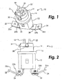
- FIG. 1 is a perspective view of a molded socket according to an embodiment of the present disclosure.
- FIG. 2 is a side elevational view of the embodiment of FIG. 1 .
- FIG. 3 is a bottom plan view of the embodiment of FIG. 1 .
- FIG. 4 is a cross-sectional view of the embodiment of FIG. 1 .
- FIG. 5 is a cross-sectional view of the embodiment of FIG. 1 installed in an exemplary lamp housing.
- FIG. 6 is a first bottom plan view of the embodiment of FIG. 1 installed in an exemplary lamp housing.
- F1G. 7 is a second bottom plan view of the embodiment of FIG. 1 installed in an exemplary lamp housing.
- the present disclosure is directed to a system which provides a connector to a lamp, wherein the connector is easily attached to a circuit board within the lamp.
- the present disclosure is directed to a system which provides a connector system for an LED lamp, where the connector easily mounts to a circuit board carrying the LEDs and provides connection points for ring terminals and/or FASTON ® terminals.
- the present disclosure is directed to a system which provides a connector system for an LED lamp, where the connector easily mounts to a circuit board carrying the LEDs and provides connection points for any design of sealed or unsealed connector.
- the present disclosure is directed to a system which provides a sealed connector system.
- an example lamp connector 10 having a first base section 12 and a second base section 14 separated by an annular sealing surface 16.
- the base sections 12, 14 and annular sealing surface 16 are formed as in integral unit, such as by injection molding a plastic material such as polyvinylchloride, to name just one non-limiting example.
- a plastic material such as polyvinylchloride
- the base sections 12, 14 and annular sealing surface 16 can be formed from any desired material or materials, using any desired forming process, and these are not critical to the presently disclosed devices and methods.
- Circuit connectors 18, 20 facilitate connection to a circuit board of the lamp (as discussed in greater detail hereinbelow). Also sealed within base sections 12, 14 and annular sealing surface 16 are two lamp connectors 22, 24. Lamp connectors 22, 24 facilitate connection of external conductive connectors to the device 10. Circuit connectors 18, 20 and lamp connectors 22, 24 are conductive. Circuit connector 18 is conductively coupled to lamp connector 22 within lamp housing sections 12, 14 and annular sealing surface 16, while circuit connector 20 is conductively coupled to lamp connector 24 within base sections 12, 14 and annular sealing surface 16. In certain embodiments, circuit connector 18 and lamp connector 22 are integrally formed, while circuit connector 20 and lamp connector 24 are integrally formed.
- lamp connector 22 includes portion 22a that allows for attachment of a FASTON ® connector thereto, and a portion 22b having a threaded connector 26 allowing for mounting of a ring terminal thereto.
- Lamp connector 24 includes portion 24a that allows for attachment of a FASTON ® connector thereto, and a portion 24b having a threaded connector 28 allowing for mounting of a ring terminal thereto.
- FASTON ® connectors are available from Amp Incorporated of Harrisburg, PA.
- base section 14 includes projecting tangs 30, 31 and 32 that facilitate retention of the device 10 within the lamp housing, as explained in greater detail hereinbelow.
- Lamp housing 52 may be coupled to a lens 54.
- the manner of coupling the lamp housing 52 and the lens 54, and whether such coupling is removable or permanent, is not critical to the present invention.
- Mounted to the lamp housing 52 is a circuit board 56 to which are mounted one or more lamps 58, such as LED lamps, to give just one non-limiting example.
- Lamp housing 52 includes a passageway 60 having an annular protrusion 62 formed therein.
- Circuit board 56 has an opening 64 formed therethrough, wherein the opening 64 is substantially aligned with the passageway 60. In some embodiments, the opening 64 has one axis that is longer than a second, transverse axis.
- Circuit board 56 further has a first conductive power connection pad 66 and a second conductive power connection pad 68 formed adjacent to opening 64.
- First conductive power connection pad 66 is provided for connection to circuit connector 18 and second conductive power connection pad 68 is provided for connection to circuit connector 20.
- first conductive power connection pad 66 and a second conductive power connection pad 68 are solder pads conductively coupled to other electronic components mounted on the circuit board 56.
- annular sealing ring 70 is mounted around the base section 14 such that it lies adjacent to annular sealing surface 16. With the lens 54 not yet coupled to the lamp housing 52, base section 14 is inserted into passageway 60 until annular sealing ring 70 is firmly compressed between annular sealing surface 16 and annular protrusion 62.
- annular protrusion 62 engages the opposite side of annular protrusion 62 in order to hold device 10 within the passageway 60 of the lamp housing 52.
- Tang 31 is provided to ensure that the base section 14 is inserted into the passageway 60 in the proper orientation, and a suitable opening (not shown) in passageway 60 ensures this.
- the sealing ring 70 is placed in compression in this position. The compression of annular sealing ring 70 inhibits the passing of moisture, dust and/or other contaminants, while also sealing the lamp housing 52 to prevent leaking of encapsulant material (if used) from inside of the lamp housing 52 trough the passageway 60.
- the circuit connectors 18, 20 have passed through the opening 64 and are positioned on the opposite side of circuit board 56 as the lamp housing section 14. Rotating the device 10 through approximately 45 degrees brings the circuit connectors 18, 20 into alignment with first conductive power connection pad 66 and a second conductive power connection pad 68, respectively. A protrusion (not shown) in the lamp housing 52 prevents the device 10 from being over-rotated during assembly.
- the circuit connector 18 may be conductively coupled to first conductive power connection pad 66 and the circuit connector 20 may be conductively coupled to second conductive power connection pad 68.
- Such conductive coupling may be made by any means known in the art, such as by soldering or welding, to give just two non-limiting examples.
- the lens 54 may be mounted to the lamp housing 52, as is known in the art.
- the device 10 is mounted within the lamp housing 52 prior to mounting the circuit board 56 to the lamp housing 52.
- the circuit board 56 is then inserted over the device 10 such that the circuit connectors 18, 20 pass through the opening 64.
- the circuit board 56 is then rotated in order to bring the circuit connectors 18, 20 into alignment with the first conductive power connection pad 66 and the second conductive power connection pad 68, respectively.
- the circuit connector 18 may be conductively coupled to first conductive power connection pad 66 and the circuit connector 20 may be conductively coupled to second conductive power connection pad 68.
- Such conductive coupling may be made by any means known in the art, such as by soldering or welding, to give just two non-limiting examples.
- the circuit board 56 may optionally be affixed to the lamp housing 52 by means other than the device 10, such as by screws or any other suitable connecting device(s). Thereafter, the lens 54 may be mounted to the lamp housing 52, as is known in the art.
- lamp connectors 22, 24 may be used to couple power from an external source, such as a vehicle power system, to the lamp(s) 58 in order to provide control in turning the lamp(s) 58 on and off.
- lamp connectors 22, 24 include portions 22a, 24a that allow for attachment of FASTON ® connectors thereto, and a portions 22b, 24b having threaded connectors 26, 28 allowing for mounting of ring terminals thereto.
- the illustrated embodiment allows easy connection of the lamp housing 52 to most existing vehicle electrical systems.
- the device 10 may have means for connecting to only a single type of connector.
- the device 10 provides connection points for any design of sealed or unsealed connector other than a FASTON ® connector or a ring terminal.
- the device 10 allows for simple and straightforward assembly of lamp connectors to a lamp housing, greatly easing the task of conductively coupling the lamp connectors to the electronic componentry of the lamp housing 52 during manufacturing.
- the present disclosure discusses the attachment of the device 10 to a circuit board incorporating LED lamps, it is contemplated that numerous types of lamps, such as incandescent and fluorescent lamps, may be used with the device 10, with the LED lamps 58 being non-limiting examples only. In addition to the numerous other types of lamps contemplated by the present disclosure, it is contemplated that a variety of other appropriate lamp housing and lens assemblies may be used with the device 10.
- the invention relates to and/or includes the following aspects:
Abstract
Description
- The present application claims the benefit of United States Provisional Patent Application Serial No.
61/295,863 filed January 18, 2010 - The present disclosure relates to electric lamps, and more particularly to a connector terminal for lamps.
- There are many lamps known in the art for various applications. To give just one example, a wide variety of lamps are used on automotive vehicles. There are expected common connection systems for such lamps, both for OEM applications and repair and retrofit applications. For example, it is extremely common for lamps to allow either ring terminal connections, connections using FASTON® connectors, or connections which are specifically shaped to mate with specific sealed and unsealed plug ins from various manufacturers such as Amp Incorporated, Delphi Corporation and Deutsch, to name just a few non-limiting examples. In certain applications, it is also a common requirement that the terminals and the lamp housing provide a sealed connection so that the interior of the lamp housing is not exposed to the elements.
- Such connection systems are relatively straightforward to manufacture in the case of incandescent or halogen sealed beam lamps, or lamps with plastic housings; however, providing such connectors in an LED lamp unit with aluminum or other metal housings for heat sinking, where the connector must be attached to a circuit board to which the LED lamps are mounted, can require quite a significant amount of hand assembly work involving the routing and soldering of wires. Additionally, providing a plurality of connection systems for a specific lamp having a plastic housing requires separate costly tooling for each different connection system.
- There is therefore a need for a system and method to provide a connector terminal for lamps. The present disclosure is directed toward systems and methods which meet this and other needs.
- An electrical connection device for a lamp housing is disclosed. The electrical connection device allows for simple and straightforward alignment of circuit connector terminals with conductive power connection pads on a lamp circuit board within a lamp housing.
- In one embodiment, a connector terminal assembly for a lamp housing is disclosed, comprising a connector housing; a first circuit connector disposed within the connector housing; a second circuit connector disposed within the connector housing; a first lamp connector disposed within the connector housing and conductively coupled to the first circuit connector; a second lamp connector disposed within the connector housing and conductively coupled to the second circuit connector; and a circuit board comprising a first circuit board surface; a circuit board opening formed through the circuit board; a first conductive power connection pad formed on the circuit board surface and disposed adjacent the circuit board opening; and a second conductive power connection pad formed on the circuit board surface and disposed adjacent the circuit board opening: wherein the circuit board is disposed between the first and second circuit connectors and the first and second lamp connectors; wherein the first and second circuit connectors may be withdrawn through the circuit board opening when the connector housing is oriented in a first position; and wherein the first and second circuit connectors may not be withdrawn through the circuit board opening when the connector housing is oriented in a second position rotated through a first angle from the first position.
- In another embodiment, a method of installing a connector terminal assembly, the method comprising the steps of: (a) providing a connector terminal assembly comprising a connector housing; a first circuit connector disposed within the connector housing, the first circuit connector having an approximately 90 degree bend formed therein; a second circuit connector disposed within the connector housing, the second circuit connector having an approximately 90 degree bend formed therein; (b) providing a circuit board a circuit board, comprising a first circuit board surface; a circuit board opening formed through the circuit board; a first conductive power connection pad formed on the circuit board surface and disposed adjacent the circuit board opening; and a second conductive power connection pad formed on the circuit board surface and disposed adjacent the circuit board opening; (c) inserting the connector terminal assembly through the circuit board opening such that the first and second circuit connectors are disposed adjacent the circuit board surface; and (d) rotating the connector housing until the first and second circuit connectors are aligned with respective ones of the first and second conductive power connection pads.
- In another embodiment, a connector terminal assembly for a lamp housing is disclosed, comprising a connector housing, a first circuit connector disposed within the connector housing, a second circuit connector disposed within the connector housing; and a circuit board comprising a first circuit board surface, and a circuit board opening formed through the circuit board, wherein the circuit board is disposed between the first and second circuit connectors and the first and second lamp connectors, wherein the first and second circuit connectors may be withdrawn through the circuit board opening when the connector housing is oriented in a first position, and wherein the first and second circuit connectors may not be withdrawn through the circuit board opening when the connector housing is oriented in a second position rotated through a first angle from the first position.
- Additional embodiments are also disclosed.
-
FIG. 1 is a perspective view of a molded socket according to an embodiment of the present disclosure. -
FIG. 2 is a side elevational view of the embodiment ofFIG. 1 . -
FIG. 3 is a bottom plan view of the embodiment ofFIG. 1 . -
FIG. 4 is a cross-sectional view of the embodiment ofFIG. 1 . -
FIG. 5 is a cross-sectional view of the embodiment ofFIG. 1 installed in an exemplary lamp housing. -
FIG. 6 is a first bottom plan view of the embodiment ofFIG. 1 installed in an exemplary lamp housing. - F1G. 7 is a second bottom plan view of the embodiment of
FIG. 1 installed in an exemplary lamp housing. - For the purposes of promoting an understanding of the principles of the disclosure, reference will now be made to the embodiments illustrated in the drawings and specific language will be used to describe the same. It will nevertheless be understood that no limitation of the scope of the disclosure is thereby intended, and alterations and modifications in the illustrated systems, and further applications of the principles of the disclosure as illustrated therein are herein contemplated as would normally occur to one skilled in the art to which the disclosure relates.
- In certain embodiments, the present disclosure is directed to a system which provides a connector to a lamp, wherein the connector is easily attached to a circuit board within the lamp.
- In certain other embodiments, the present disclosure is directed to a system which provides a connector system for an LED lamp, where the connector easily mounts to a circuit board carrying the LEDs and provides connection points for ring terminals and/or FASTON® terminals. In other embodiments, the present disclosure is directed to a system which provides a connector system for an LED lamp, where the connector easily mounts to a circuit board carrying the LEDs and provides connection points for any design of sealed or unsealed connector. In certain embodiments, the present disclosure is directed to a system which provides a sealed connector system.
- Referring to
Figs. 1-4 , there is shown anexample lamp connector 10 having afirst base section 12 and asecond base section 14 separated by anannular sealing surface 16. In certain embodiments, thebase sections annular sealing surface 16 are formed as in integral unit, such as by injection molding a plastic material such as polyvinylchloride, to name just one non-limiting example. Those skilled in the art will recognize that thebase sections annular sealing surface 16 can be formed from any desired material or materials, using any desired forming process, and these are not critical to the presently disclosed devices and methods. - Sealed within
base sections annular sealing surface 16 are twocircuit connectors Circuit connectors base sections annular sealing surface 16 are twolamp connectors Lamp connectors device 10.Circuit connectors lamp connectors Circuit connector 18 is conductively coupled tolamp connector 22 withinlamp housing sections annular sealing surface 16, whilecircuit connector 20 is conductively coupled tolamp connector 24 withinbase sections annular sealing surface 16. In certain embodiments,circuit connector 18 andlamp connector 22 are integrally formed, whilecircuit connector 20 andlamp connector 24 are integrally formed. - In some embodiments,
lamp connector 22 includesportion 22a that allows for attachment of a FASTON® connector thereto, and aportion 22b having a threadedconnector 26 allowing for mounting of a ring terminal thereto.Lamp connector 24 includesportion 24a that allows for attachment of a FASTON® connector thereto, and aportion 24b having a threadedconnector 28 allowing for mounting of a ring terminal thereto. Those skilled in the art will recognize that FASTON® connectors are available from Amp Incorporated of Harrisburg, PA. In certain embodiments,base section 14 includes projectingtangs device 10 within the lamp housing, as explained in greater detail hereinbelow. - Referring now to
Figs. 5-7 , one embodiment of thedevice 10 is shown mounted to anexemplary lamp housing 52.Lamp housing 52 may be coupled to alens 54. The manner of coupling the lamp housing 52 and thelens 54, and whether such coupling is removable or permanent, is not critical to the present invention. Mounted to thelamp housing 52 is acircuit board 56 to which are mounted one ormore lamps 58, such as LED lamps, to give just one non-limiting example. -
Lamp housing 52 includes apassageway 60 having anannular protrusion 62 formed therein.Circuit board 56 has an opening 64 formed therethrough, wherein theopening 64 is substantially aligned with thepassageway 60. In some embodiments, theopening 64 has one axis that is longer than a second, transverse axis.Circuit board 56 further has a first conductivepower connection pad 66 and a second conductivepower connection pad 68 formed adjacent to opening 64. First conductivepower connection pad 66 is provided for connection tocircuit connector 18 and second conductivepower connection pad 68 is provided for connection tocircuit connector 20. In some embodiments, first conductivepower connection pad 66 and a second conductivepower connection pad 68 are solder pads conductively coupled to other electronic components mounted on thecircuit board 56. - With continuing reference to
Figs. 5-7 , mounting of thedevice 10 to thelamp housing 52 will now be described. An optionalannular sealing ring 70 is mounted around thebase section 14 such that it lies adjacent toannular sealing surface 16. With thelens 54 not yet coupled to thelamp housing 52,base section 14 is inserted intopassageway 60 untilannular sealing ring 70 is firmly compressed betweenannular sealing surface 16 andannular protrusion 62. - Projecting tangs 30 and 32 engage the opposite side of
annular protrusion 62 in order to holddevice 10 within thepassageway 60 of thelamp housing 52. Tang 31 is provided to ensure that thebase section 14 is inserted into thepassageway 60 in the proper orientation, and a suitable opening (not shown) inpassageway 60 ensures this. In some embodiments, the sealingring 70 is placed in compression in this position. The compression ofannular sealing ring 70 inhibits the passing of moisture, dust and/or other contaminants, while also sealing thelamp housing 52 to prevent leaking of encapsulant material (if used) from inside of thelamp housing 52 trough thepassageway 60. - In this position of the
device 10, thecircuit connectors opening 64 and are positioned on the opposite side ofcircuit board 56 as thelamp housing section 14. Rotating thedevice 10 through approximately 45 degrees brings thecircuit connectors power connection pad 66 and a second conductivepower connection pad 68, respectively. A protrusion (not shown) in thelamp housing 52 prevents thedevice 10 from being over-rotated during assembly. Once aligned, thecircuit connector 18 may be conductively coupled to first conductivepower connection pad 66 and thecircuit connector 20 may be conductively coupled to second conductivepower connection pad 68. Such conductive coupling may be made by any means known in the art, such as by soldering or welding, to give just two non-limiting examples. Thereafter, thelens 54 may be mounted to thelamp housing 52, as is known in the art. - In other embodiments, the
device 10 is mounted within thelamp housing 52 prior to mounting thecircuit board 56 to thelamp housing 52. Thecircuit board 56 is then inserted over thedevice 10 such that thecircuit connectors opening 64. Thecircuit board 56 is then rotated in order to bring thecircuit connectors power connection pad 66 and the second conductivepower connection pad 68, respectively. Once aligned, thecircuit connector 18 may be conductively coupled to first conductivepower connection pad 66 and thecircuit connector 20 may be conductively coupled to second conductivepower connection pad 68. Such conductive coupling may be made by any means known in the art, such as by soldering or welding, to give just two non-limiting examples. Thecircuit board 56 may optionally be affixed to thelamp housing 52 by means other than thedevice 10, such as by screws or any other suitable connecting device(s). Thereafter, thelens 54 may be mounted to thelamp housing 52, as is known in the art. - Once the
device 10 is mounted to the lamp housing 50,lamp connectors lamp connectors portions portions connectors lamp housing 52 to most existing vehicle electrical systems. In other embodiments, thedevice 10 may have means for connecting to only a single type of connector. In other embodiments, thedevice 10 provides connection points for any design of sealed or unsealed connector other than a FASTON® connector or a ring terminal. - It will be appreciated that the
device 10 allows for simple and straightforward assembly of lamp connectors to a lamp housing, greatly easing the task of conductively coupling the lamp connectors to the electronic componentry of thelamp housing 52 during manufacturing. - It should be appreciated that although the present disclosure discusses the attachment of the
device 10 to a circuit board incorporating LED lamps, it is contemplated that numerous types of lamps, such as incandescent and fluorescent lamps, may be used with thedevice 10, with theLED lamps 58 being non-limiting examples only. In addition to the numerous other types of lamps contemplated by the present disclosure, it is contemplated that a variety of other appropriate lamp housing and lens assemblies may be used with thedevice 10. - While the disclosure has been illustrated and described in detail in the drawings and foregoing description, the same is to be considered as illustrative and not restrictive in character, it being understood that only certain embodiments have been shown and described and that all changes and modifications that come within the spirit of the disclosure are desired to be protected.
- The invention relates to and/or includes the following aspects:
- 1. A connector terminal assembly for a lamp housing, comprising:
- a connector housing;
- a first circuit connector disposed within the connector housing;
- a second circuit connector disposed within the connector housing;
- a first lamp connector disposed within the connector housing and conductively
coupled to the first circuit connector; - a second lamp connector disposed within the connector housing and conductively
coupled to the second circuit connector; and - a circuit board comprising:
- a first circuit board surface;
- a circuit board opening formed through the circuit board;
- a first conductive power connection pad formed on the circuit board
- surface and disposed adjacent the circuit board opening; and a second conductive power connection pad formed on the circuit board surface and disposed adjacent the circuit board opening;
wherein the fist and second circuit connectors may be withdrawn through the circuit board opening when the connector housing is oriented in a first position; and
wherein the first and second circuit connectors may not be withdrawn through the circuit board opening when the connector housing is oriented in a second position rotated through a first angle from the first position.
- 2. The connector terminal assembly of aspect 1, wherein said connector housing comprises:
- a first base section;
- a second base section; and
- an annular sealing surface disposed between the first and second base sections.
- 3. The connector terminal assembly of aspect 2, wherein the first base section, the annular sealing surface and the second base section comprise an integral plastic housing.
- 4. The connector terminal assembly of aspect 1, wherein:
- the first circuit connector and the first lamp connector comprise a first integral
conductive member; and - the second circuit connector and the second lamp connector comprise a second
integral conductive member.
- the first circuit connector and the first lamp connector comprise a first integral
- 5. The connector terminal assembly of aspect 1, wherein the first and second lamp connector each comprise:
- an attachment area for receiving a FASTON® connector; and
- a threaded connector for receiving a ring terminal.
- 6. The connector terminal assembly of aspect 1, wherein the first and second circuit connectors each comprise a conductive element having an approximately 90 degree bend therein.
- 7. The connector terminal assembly of aspect 1, further comprising:
- at least one tang projecting from a surface of the connector housing, the at least one tang operative to secure the connector housing in a lamp housing
- 8. The connector terminal assembly of aspect 1, wherein:
- the circuit board opening has a longitudinal axis and a transverse axis; and
- a first dimension of the circuit board opening along the longitudinal axis is greater
than a second dimension of the circuit board opening along the transverse axis.
- 9. The connector terminal assembly of aspect 1, further comprising:
- a lamp housing having a lamp housing opening formed therethrough;
wherein the connector housing extends through the lamp housing opening. - 10. The connector terminal assembly of aspect 9, further comprising a lens coupled to the lamp housing.
- 11. The connector terminal assembly of aspect 1, further comprising at least one LED lamp mounted to the circuit board.
- 12. The connector terminal assembly of aspect 1, wherein the first and second circuit connectors are conductively coupled to respective ones of the first and second conductive power connection pads.
- 13. The connector terminal assembly of
aspect 12, wherein the first and second circuit connectors are soldered to respective ones of the first and second conductive power connection pads. - 14. A connector terminal assembly for a lamp housing, comprising:
- a connector housing;
- a first circuit connector disposed within the connector housing;
- a second circuit connector disposed within the connector housing; and
- a circuit board comprising:
- a first circuit board surface; and
- a circuit board opening formed through the circuit board;
connectors and the first and second lamp connectors;
wherein the first and second circuit connectors may be withdrawn through the
circuit board opening when the connector housing is oriented in a first position; and
wherein the first and second circuit connectors may not be withdrawn through the
circuit board opening when the connector housing is oriented in a second position rotated through a first angle from the first position. - 15. The connector terminal assembly of
aspect 14, further comprising:- a first lamp connector disposed within the connector housing and conductively
coupled to the first circuit connector; and - a second lamp connector disposed within the connector housing and conductively
coupled to the second circuit connector.
- a first lamp connector disposed within the connector housing and conductively
- 16. The connector terminal assembly of
aspect 14, further comprising:- a first conductive power connection pad formed on the circuit board surface and
disposed adjacent the circuit board opening; and - a second conductive power connection pad formed on the circuit board surface
and disposed adjacent the circuit board opening.
- a first conductive power connection pad formed on the circuit board surface and
- 17. The connector terminal assembly of
aspect 14, wherein said connector housing comprises:- a first base section;
- a second base section: and
- an annular sealing surface disposed between the first and second base sections.
- 18. The connector terminal assembly of aspect 17, wherein the first base section, the annular sealing surface and the second base section comprise an integral plastic housing.
- 19. The connector terminal assembly of aspect 15, wherein:
- the first circuit connector and the first lamp connector comprise a first integral
conductive member; and - the second circuit connector and the second lamp connector comprise a second
integral conductive member.
- the first circuit connector and the first lamp connector comprise a first integral
- 20. The connector terminal assembly of aspect 15, wherein the first and second lamp connector each comprise:
- an attachment area for receiving a FASTON® connector; and
- a threaded connector for receiving a ring terminal.
- 21. The connector terminal assembly of
aspect 14, wherein the first and second circuit connectors each comprise a conductive element having an approximately 90 degree bend therein. - 22. The connector terminal assembly of
aspect 14, further comprising:- at least one tang projecting from a surface of the connector housing, the at least one tang operative to secure the connector housing in a lamp housing
- 23. The connector terminal assembly of
aspect 14, wherein:- the circuit board opening has a longitudinal axis and a transverse axis; and
- a first dimension of the circuit board opening along the longitudinal axis is greater
than a second dimension of the circuit board opening along the transverse axis.
- 24. The connector terminal assembly of
aspect 14, further comprising:- a lamp housing having a lamp housing opening formed therethrough;
wherein the connector housing extends through the lamp housing opening. - 25. The connector terminal assembly of
aspect 24, further comprising a lens coupled to the lamp housing. - 26. The connector terminal assembly of
aspect 14, further comprising at least one LED lamp mounted to the circuit board. - 27. The connector terminal assembly of
aspect 16, wherein the first and second circuit connectors are conductively coupled to respective ones of the first and second conductive power connection pads. - 28. The connector terminal assembly of aspect 27, wherein the first and second circuit connectors are soldered to respective ones of the first and second conductive power connection pads.
- 29. A method of installing a connector terminal assembly, the method comprising the steps of:
- (a) providing a connector terminal assembly comprising:
- a connector housing;
- a first circuit connector disposed within the connector housing, the first circuit
connector having an approximately 90 degree bend formed therein; - a second circuit connector disposed within the connector housing, the second
circuit connector having an approximately 90 degree bend formed therein;
- (b) providing a circuit board a circuit board, comprising:
- a first circuit board surface;
- a circuit board opening formed through the circuit board;
- a first conductive power connection pad formed on the circuit board
surface and disposed adjacent the circuit board opening; and - a second conductive power connection pad formed on the circuit board
surface and disposed adjacent the circuit board opening;
- (c) inserting the connector terminal assembly through the circuit board opening such that the first and second circuit connectors are disposed adjacent the circuit board surface; and
- (d) rotating the connector housing until the first and second circuit connectors are aligned with respective ones of the first and second conductive power connection pads.
- (a) providing a connector terminal assembly comprising:
- 30. The method of aspect 29, further comprising the step of:
- (e) forming a conductive coupling between the first and second circuit connectors and respective ones of the first and second conductive power connection pads.
- 31. The method of
aspect 30, wherein the step of forming a conductive coupling comprises soldering. - 32. The method of
aspect 30, wherein the step of forming a conductive coupling comprises welding.
Claims (15)
- A connector terminal assembly for a lamp housing, comprising:a connector housing;a first circuit connector disposed within the connector housing;a second circuit connector disposed within the connector housing; anda circuit board comprising:wherein the circuit board is disposed between the first and second circuita first circuit board surface; anda circuit board opening formed through the circuit board;
connectors;
wherein the first and second circuit connectors may be withdrawn through the
circuit board opening when the connector housing is oriented in a first position; and
wherein the first and second circuit connectors may not be withdrawn through the
circuit board opening when the connector housing is oriented in a second position rotated through a first angle from the first position. - The connector terminal assembly of claim 1, further comprising:a first lamp connector disposed within the connector housing and conductively
coupled to the first circuit connector; anda second lamp connector disposed within the connector housing and conductively
coupled to the second circuit connector,and/or wherein, optionally, the circuit board is disposed between the first and
second lamp connectors. - The connector terminal assembly of claim 1 or claim 2, further comprising:a first conductive power connection pad formed on the circuit board surface and
disposed adjacent the circuit board opening; anda second conductive power connection pad formed on the circuit board surface
and disposed adjacent the circuit board opening. - The connector terminal assembly of any preceding claim, wherein said connector housing comprises:a first base section:a second base section; andan annular sealing surface disposed between the first and second base sections,and wherein, optionally, the first base section, the annular sealing surface and the
second base section comprise an integral plastic housing. - The connector terminal assembly of any preceding claim when dependent on claim 2, wherein:the first circuit connector and the first lamp connector comprise a first integral
conductive member; andthe second circuit connector and the second lamp connector comprise a second
integral conductive member. - The connector terminal assembly of any preceding claim when dependent on claim 2, wherein the first and second lamp connector each comprise:an attachment area for receiving a FASTON® connector; anda threaded connector for receiving a ring terminal.
- The connector terminal assembly of any preceding claim, wherein the first and second circuit connectors each comprise a conductive element having an approximately 90 degree bend therein.
- The connector terminal assembly of any preceding claim, further comprising:at least one tang projecting from a surface of the connector housing, the at least
one tang operative to secure the connector housing in a lamp housing when mounted therein. - The connector terminal assembly of any preceding claim, wherein:the circuit board opening has a longitudinal axis and a transverse axis; anda first dimension of the circuit board opening along the longitudinal axis is greater
than a second dimension of the circuit board opening along the transverse axis. - The connector terminal assembly of any preceding claim, further comprising a lamp housing having a lamp housing opening formed therethrough;
wherein the circuit board is coupled to the lamp housing; and
wherein the connector housing extends through the lamp housing opening,
and wherein
the connector terminal assembly may, optionally, further comprise a lens coupled to the lamp housing. - The connector terminal assembly of any preceding claim, further comprising at least one LED lamp mounted to the circuit board.
- The connector terminal assembly of any preceding claim when dependent on claim 3, wherein the first and second circuit connectors are conductively coupled to respective ones of the first and second conductive power connection pads, and/or
wherein the first and second circuit connectors are soldered to respective ones of the first and second conductive power connection pads. - A method of installing a connector terminal assembly, the method comprising the steps of:(a) providing a connector terminal assembly comprising:a connector housing;a first circuit connector disposed within the connector housing, the first circuit
connector having an approximately 90 degree bend formed therein;a second circuit connector disposed within the connector housing, the second
circuit connector having an approximately 90 degree bend formed therein:(b) providing a circuit board a circuit board, comprising:a first circuit board surface;a circuit board opening formed through the circuit board;a first conductive power connection pad formed on the circuit board
surface and disposed adjacent the circuit board opening; anda second conductive power connection pad formed on the circuit board
surface and disposed adjacent the circuit board opening;(c) inserting the connector terminal assembly through the circuit board opening such that the first and second circuit connectors are disposed adjacent the circuit board surface; and(d) rotating the connector housing until the first and second circuit connectors are aligned with respective ones of the first and second conductive power connection pads. - The method of claim 15, further comprising the step of:(e) forming a conductive coupling between the first and second circuit connectors and respective ones of the first and second conductive power connection pads.
- The method of claim 14, wherein the step of forming a conductive coupling comprises soldering and/or welding.
Priority Applications (1)
| Application Number | Priority Date | Filing Date | Title |
|---|---|---|---|
| PL11250052T PL2345840T3 (en) | 2010-01-18 | 2011-01-18 | Connector terminal for lamps |
Applications Claiming Priority (1)
| Application Number | Priority Date | Filing Date | Title |
|---|---|---|---|
| US29586310P | 2010-01-18 | 2010-01-18 |
Publications (3)
| Publication Number | Publication Date |
|---|---|
| EP2345840A2 true EP2345840A2 (en) | 2011-07-20 |
| EP2345840A3 EP2345840A3 (en) | 2012-10-31 |
| EP2345840B1 EP2345840B1 (en) | 2015-07-29 |
Family
ID=43629541
Family Applications (1)
| Application Number | Title | Priority Date | Filing Date |
|---|---|---|---|
| EP11250052.5A Active EP2345840B1 (en) | 2010-01-18 | 2011-01-18 | Connector terminal for lamps |
Country Status (8)
| Country | Link |
|---|---|
| US (1) | US8469719B2 (en) |
| EP (1) | EP2345840B1 (en) |
| CA (1) | CA2728372C (en) |
| DK (1) | DK2345840T3 (en) |
| ES (1) | ES2548054T3 (en) |
| MX (1) | MX2011000685A (en) |
| PL (1) | PL2345840T3 (en) |
| PT (1) | PT2345840E (en) |
Cited By (4)
| Publication number | Priority date | Publication date | Assignee | Title |
|---|---|---|---|---|
| EP2492591A3 (en) * | 2011-02-28 | 2013-03-27 | Panasonic Corporation | Led unit and illumination apparatus using same |
| FR2998087A1 (en) * | 2012-11-09 | 2014-05-16 | Legrand France | Luminous indicator for switchgear such as electric switch mechanism, has connection pins crossing plate such that one of ends of each pin is accessible on side of front face of plate, and is connected electrically to electrical circuit |
| WO2016113114A1 (en) * | 2015-01-13 | 2016-07-21 | Philips Lighting Holding B.V. | A lighting device comprising an improved optical element |
| WO2024044829A1 (en) | 2022-09-02 | 2024-03-07 | Balbinot Mauricio | Structural arrangement in an electrical connection applied to a vehicle lamp |
Families Citing this family (1)
| Publication number | Priority date | Publication date | Assignee | Title |
|---|---|---|---|---|
| CN104251390A (en) * | 2013-06-27 | 2014-12-31 | 欧普照明股份有限公司 | Lamp |
Family Cites Families (12)
| Publication number | Priority date | Publication date | Assignee | Title |
|---|---|---|---|---|
| GB1464598A (en) | 1974-02-19 | 1977-02-16 | Carr Fastener Co Ltd | Lampholder for wedge base lamps |
| GB1602527A (en) * | 1978-05-30 | 1981-11-11 | Ford Motor Co | Bulbholder and filter assembly |
| US4593958A (en) * | 1984-05-04 | 1986-06-10 | Kabushiki Kaisha Toshiba | Socket for baseless lamp |
| US4628421A (en) * | 1986-01-23 | 1986-12-09 | Saar Lawrence E | Strip lighting |
| US4965457A (en) | 1989-02-17 | 1990-10-23 | Avi Wrobel | Removable panel illuminating module |
| US5536175A (en) * | 1994-09-29 | 1996-07-16 | Cooper Industries, Inc. | Backplate assembly and method of making same |
| DE19705738C2 (en) | 1997-02-14 | 1999-02-18 | Trw Fahrzeugelektrik | Socket for a lighting element for installation in a printed circuit board, in particular for illuminating function symbols or for signaling functions in motor vehicles |
| US5947588A (en) | 1997-10-06 | 1999-09-07 | Grand General Accessories Manufacturing Inc. | Light fixture with an LED light bulb having a conventional connection post |
| US6135780A (en) * | 1999-11-22 | 2000-10-24 | Navistar International Transportation Corp | Dual function lamp socket |
| JP2004523868A (en) * | 2001-01-18 | 2004-08-05 | メリディアン オートモーティブ システムズ インコーポレイテッド | Method for vacuum depositing a circuit on a thermoplastic material and a vehicle lamp housing containing the circuit |
| JP2002343104A (en) | 2001-05-21 | 2002-11-29 | Hitachi Building Systems Co Ltd | Led assembly lamp |
| US6729020B2 (en) * | 2002-04-01 | 2004-05-04 | International Truck Intellectual Property Company, Llc | Method for replacing a board-mounted electric circuit component |
-
2011
- 2011-01-13 US US13/006,035 patent/US8469719B2/en active Active
- 2011-01-17 CA CA2728372A patent/CA2728372C/en active Active
- 2011-01-17 MX MX2011000685A patent/MX2011000685A/en active IP Right Grant
- 2011-01-18 DK DK11250052.5T patent/DK2345840T3/en active
- 2011-01-18 EP EP11250052.5A patent/EP2345840B1/en active Active
- 2011-01-18 PT PT112500525T patent/PT2345840E/en unknown
- 2011-01-18 PL PL11250052T patent/PL2345840T3/en unknown
- 2011-01-18 ES ES11250052.5T patent/ES2548054T3/en active Active
Cited By (6)
| Publication number | Priority date | Publication date | Assignee | Title |
|---|---|---|---|---|
| EP2492591A3 (en) * | 2011-02-28 | 2013-03-27 | Panasonic Corporation | Led unit and illumination apparatus using same |
| US8684568B2 (en) | 2011-02-28 | 2014-04-01 | Panasonic Corporation | LED unit and illumination apparatus using same |
| FR2998087A1 (en) * | 2012-11-09 | 2014-05-16 | Legrand France | Luminous indicator for switchgear such as electric switch mechanism, has connection pins crossing plate such that one of ends of each pin is accessible on side of front face of plate, and is connected electrically to electrical circuit |
| WO2016113114A1 (en) * | 2015-01-13 | 2016-07-21 | Philips Lighting Holding B.V. | A lighting device comprising an improved optical element |
| US10465899B2 (en) | 2015-01-13 | 2019-11-05 | Signify Holding B.V. | Lighting device comprising an improved optical element |
| WO2024044829A1 (en) | 2022-09-02 | 2024-03-07 | Balbinot Mauricio | Structural arrangement in an electrical connection applied to a vehicle lamp |
Also Published As
| Publication number | Publication date |
|---|---|
| PL2345840T3 (en) | 2016-01-29 |
| CA2728372C (en) | 2014-04-22 |
| EP2345840A3 (en) | 2012-10-31 |
| MX2011000685A (en) | 2011-07-18 |
| CA2728372A1 (en) | 2011-07-18 |
| DK2345840T3 (en) | 2015-11-09 |
| EP2345840B1 (en) | 2015-07-29 |
| US8469719B2 (en) | 2013-06-25 |
| US20120021656A1 (en) | 2012-01-26 |
| PT2345840E (en) | 2015-10-19 |
| ES2548054T3 (en) | 2015-10-13 |
Similar Documents
| Publication | Publication Date | Title |
|---|---|---|
| US7704082B2 (en) | Through board inverted connector | |
| EP2802811B1 (en) | Solid state lighting assembly | |
| AU2006228019A1 (en) | Metal carrier for LEDs in composite lamps | |
| JP5598758B2 (en) | connector | |
| TWI490429B (en) | A method of mounting a led module to a heat sink | |
| US10222023B2 (en) | Lighting module comprising at least one component and a connector which are disposed on a heat dissipater, and lighting device for automotive vehicle comprising such a module | |
| US8469719B2 (en) | Connector terminal for lamps | |
| EP3382269B1 (en) | A folded heat sink with electrical connection protection | |
| CN104466564B (en) | Electronic module with side entrance connection | |
| EP2871721A1 (en) | Connecting structure for terminal fitting and substrate | |
| US9172162B2 (en) | Circuit board connector | |
| CN106523942B (en) | Heat sink with integrated electrical and base contacts | |
| CN108232496B (en) | Electronic device | |
| KR101728918B1 (en) | Connector for Socket and using this LED bulb | |
| US11006540B2 (en) | Circuit board for mechanically fastening a housing | |
| US10305208B2 (en) | Electronic device | |
| CN103196042B (en) | Illuminator and manufacture method thereof | |
| CN113748297A (en) | Lighting device with high flexibility in connecting electrical components | |
| JP2002246081A (en) | Terminal block with temperature fuse connection contact | |
| CN202432458U (en) | Light emitting diode (LED) illuminating device with electrical interconnecting part | |
| WO2017218510A1 (en) | Clip unit and edge mounted light emitting diode (led) assembly comprising a clip unit | |
| CN105552610B (en) | Connector device | |
| JP6690123B2 (en) | Base for lighting lamp, lighting lamp and lighting device | |
| JP2000207906A (en) | Wiring part of vehicle lighting fixture | |
| JP6499531B2 (en) | Electrical connector |
Legal Events
| Date | Code | Title | Description |
|---|---|---|---|
| PUAI | Public reference made under article 153(3) epc to a published international application that has entered the european phase |
Free format text: ORIGINAL CODE: 0009012 |
|
| AK | Designated contracting states |
Kind code of ref document: A2 Designated state(s): AL AT BE BG CH CY CZ DE DK EE ES FI FR GB GR HR HU IE IS IT LI LT LU LV MC MK MT NL NO PL PT RO RS SE SI SK SM TR |
|
| AX | Request for extension of the european patent |
Extension state: BA ME |
|
| PUAL | Search report despatched |
Free format text: ORIGINAL CODE: 0009013 |
|
| AK | Designated contracting states |
Kind code of ref document: A3 Designated state(s): AL AT BE BG CH CY CZ DE DK EE ES FI FR GB GR HR HU IE IS IT LI LT LU LV MC MK MT NL NO PL PT RO RS SE SI SK SM TR |
|
| AX | Request for extension of the european patent |
Extension state: BA ME |
|
| RIC1 | Information provided on ipc code assigned before grant |
Ipc: F21V 31/00 20060101ALN20120927BHEP Ipc: F21V 5/04 20060101ALN20120927BHEP Ipc: F21K 99/00 20100101ALI20120927BHEP Ipc: F21V 23/06 20060101AFI20120927BHEP Ipc: F21Y 101/02 20060101ALN20120927BHEP |
|
| 17P | Request for examination filed |
Effective date: 20130430 |
|
| GRAP | Despatch of communication of intention to grant a patent |
Free format text: ORIGINAL CODE: EPIDOSNIGR1 |
|
| RIC1 | Information provided on ipc code assigned before grant |
Ipc: F21V 23/06 20060101AFI20150203BHEP Ipc: F21Y 101/02 20060101ALN20150203BHEP Ipc: F21V 31/00 20060101ALN20150203BHEP Ipc: F21V 5/04 20060101ALN20150203BHEP Ipc: F21K 99/00 20100101ALI20150203BHEP |
|
| INTG | Intention to grant announced |
Effective date: 20150220 |
|
| GRAS | Grant fee paid |
Free format text: ORIGINAL CODE: EPIDOSNIGR3 |
|
| GRAA | (expected) grant |
Free format text: ORIGINAL CODE: 0009210 |
|
| AK | Designated contracting states |
Kind code of ref document: B1 Designated state(s): AL AT BE BG CH CY CZ DE DK EE ES FI FR GB GR HR HU IE IS IT LI LT LU LV MC MK MT NL NO PL PT RO RS SE SI SK SM TR |
|
| REG | Reference to a national code |
Ref country code: GB Ref legal event code: FG4D |
|
| REG | Reference to a national code |
Ref country code: CH Ref legal event code: EP |
|
| REG | Reference to a national code |
Ref country code: AT Ref legal event code: REF Ref document number: 739622 Country of ref document: AT Kind code of ref document: T Effective date: 20150815 |
|
| REG | Reference to a national code |
Ref country code: IE Ref legal event code: FG4D |
|
| REG | Reference to a national code |
Ref country code: DE Ref legal event code: R096 Ref document number: 602011018189 Country of ref document: DE |
|
| REG | Reference to a national code |
Ref country code: ES Ref legal event code: FG2A Ref document number: 2548054 Country of ref document: ES Kind code of ref document: T3 Effective date: 20151013 |
|
| REG | Reference to a national code |
Ref country code: PT Ref legal event code: SC4A Free format text: AVAILABILITY OF NATIONAL TRANSLATION Effective date: 20150922 |
|
| REG | Reference to a national code |
Ref country code: CH Ref legal event code: NV Representative=s name: MARKS AND CLERK (LUXEMBOURG) LLP, CH |
|
| REG | Reference to a national code |
Ref country code: DK Ref legal event code: T3 Effective date: 20151102 |
|
| REG | Reference to a national code |
Ref country code: SE Ref legal event code: TRGR |
|
| REG | Reference to a national code |
Ref country code: FR Ref legal event code: PLFP Year of fee payment: 6 |
|
| REG | Reference to a national code |
Ref country code: NL Ref legal event code: FP |
|
| REG | Reference to a national code |
Ref country code: NO Ref legal event code: T2 Effective date: 20150729 |
|
| REG | Reference to a national code |
Ref country code: LT Ref legal event code: MG4D |
|
| PG25 | Lapsed in a contracting state [announced via postgrant information from national office to epo] |
Ref country code: LV Free format text: LAPSE BECAUSE OF FAILURE TO SUBMIT A TRANSLATION OF THE DESCRIPTION OR TO PAY THE FEE WITHIN THE PRESCRIBED TIME-LIMIT Effective date: 20150729 Ref country code: LT Free format text: LAPSE BECAUSE OF FAILURE TO SUBMIT A TRANSLATION OF THE DESCRIPTION OR TO PAY THE FEE WITHIN THE PRESCRIBED TIME-LIMIT Effective date: 20150729 |
|
| PG25 | Lapsed in a contracting state [announced via postgrant information from national office to epo] |
Ref country code: RS Free format text: LAPSE BECAUSE OF FAILURE TO SUBMIT A TRANSLATION OF THE DESCRIPTION OR TO PAY THE FEE WITHIN THE PRESCRIBED TIME-LIMIT Effective date: 20150729 Ref country code: HR Free format text: LAPSE BECAUSE OF FAILURE TO SUBMIT A TRANSLATION OF THE DESCRIPTION OR TO PAY THE FEE WITHIN THE PRESCRIBED TIME-LIMIT Effective date: 20150729 |
|
| REG | Reference to a national code |
Ref country code: GR Ref legal event code: EP Ref document number: 20150402235 Country of ref document: GR Effective date: 20151209 |
|
| PG25 | Lapsed in a contracting state [announced via postgrant information from national office to epo] |
Ref country code: SK Free format text: LAPSE BECAUSE OF FAILURE TO SUBMIT A TRANSLATION OF THE DESCRIPTION OR TO PAY THE FEE WITHIN THE PRESCRIBED TIME-LIMIT Effective date: 20150729 Ref country code: CZ Free format text: LAPSE BECAUSE OF FAILURE TO SUBMIT A TRANSLATION OF THE DESCRIPTION OR TO PAY THE FEE WITHIN THE PRESCRIBED TIME-LIMIT Effective date: 20150729 Ref country code: EE Free format text: LAPSE BECAUSE OF FAILURE TO SUBMIT A TRANSLATION OF THE DESCRIPTION OR TO PAY THE FEE WITHIN THE PRESCRIBED TIME-LIMIT Effective date: 20150729 |
|
| REG | Reference to a national code |
Ref country code: DE Ref legal event code: R097 Ref document number: 602011018189 Country of ref document: DE |
|
| PG25 | Lapsed in a contracting state [announced via postgrant information from national office to epo] |
Ref country code: RO Free format text: LAPSE BECAUSE OF FAILURE TO SUBMIT A TRANSLATION OF THE DESCRIPTION OR TO PAY THE FEE WITHIN THE PRESCRIBED TIME-LIMIT Effective date: 20150729 |
|
| PLBE | No opposition filed within time limit |
Free format text: ORIGINAL CODE: 0009261 |
|
| STAA | Information on the status of an ep patent application or granted ep patent |
Free format text: STATUS: NO OPPOSITION FILED WITHIN TIME LIMIT |
|
| 26N | No opposition filed |
Effective date: 20160502 |
|
| PG25 | Lapsed in a contracting state [announced via postgrant information from national office to epo] |
Ref country code: SI Free format text: LAPSE BECAUSE OF FAILURE TO SUBMIT A TRANSLATION OF THE DESCRIPTION OR TO PAY THE FEE WITHIN THE PRESCRIBED TIME-LIMIT Effective date: 20150729 Ref country code: LU Free format text: LAPSE BECAUSE OF FAILURE TO SUBMIT A TRANSLATION OF THE DESCRIPTION OR TO PAY THE FEE WITHIN THE PRESCRIBED TIME-LIMIT Effective date: 20160118 |
|
| PG25 | Lapsed in a contracting state [announced via postgrant information from national office to epo] |
Ref country code: MC Free format text: LAPSE BECAUSE OF FAILURE TO SUBMIT A TRANSLATION OF THE DESCRIPTION OR TO PAY THE FEE WITHIN THE PRESCRIBED TIME-LIMIT Effective date: 20150729 |
|
| REG | Reference to a national code |
Ref country code: FR Ref legal event code: PLFP Year of fee payment: 7 |
|
| REG | Reference to a national code |
Ref country code: AT Ref legal event code: UEP Ref document number: 739622 Country of ref document: AT Kind code of ref document: T Effective date: 20150729 |
|
| PG25 | Lapsed in a contracting state [announced via postgrant information from national office to epo] |
Ref country code: MT Free format text: LAPSE BECAUSE OF FAILURE TO SUBMIT A TRANSLATION OF THE DESCRIPTION OR TO PAY THE FEE WITHIN THE PRESCRIBED TIME-LIMIT Effective date: 20150729 |
|
| REG | Reference to a national code |
Ref country code: FR Ref legal event code: PLFP Year of fee payment: 8 |
|
| PG25 | Lapsed in a contracting state [announced via postgrant information from national office to epo] |
Ref country code: SM Free format text: LAPSE BECAUSE OF FAILURE TO SUBMIT A TRANSLATION OF THE DESCRIPTION OR TO PAY THE FEE WITHIN THE PRESCRIBED TIME-LIMIT Effective date: 20150729 Ref country code: HU Free format text: LAPSE BECAUSE OF FAILURE TO SUBMIT A TRANSLATION OF THE DESCRIPTION OR TO PAY THE FEE WITHIN THE PRESCRIBED TIME-LIMIT; INVALID AB INITIO Effective date: 20110118 Ref country code: CY Free format text: LAPSE BECAUSE OF FAILURE TO SUBMIT A TRANSLATION OF THE DESCRIPTION OR TO PAY THE FEE WITHIN THE PRESCRIBED TIME-LIMIT Effective date: 20150729 |
|
| PG25 | Lapsed in a contracting state [announced via postgrant information from national office to epo] |
Ref country code: MK Free format text: LAPSE BECAUSE OF FAILURE TO SUBMIT A TRANSLATION OF THE DESCRIPTION OR TO PAY THE FEE WITHIN THE PRESCRIBED TIME-LIMIT Effective date: 20150729 Ref country code: MT Free format text: LAPSE BECAUSE OF FAILURE TO SUBMIT A TRANSLATION OF THE DESCRIPTION OR TO PAY THE FEE WITHIN THE PRESCRIBED TIME-LIMIT Effective date: 20160131 Ref country code: TR Free format text: LAPSE BECAUSE OF FAILURE TO SUBMIT A TRANSLATION OF THE DESCRIPTION OR TO PAY THE FEE WITHIN THE PRESCRIBED TIME-LIMIT Effective date: 20150729 |
|
| PG25 | Lapsed in a contracting state [announced via postgrant information from national office to epo] |
Ref country code: BG Free format text: LAPSE BECAUSE OF FAILURE TO SUBMIT A TRANSLATION OF THE DESCRIPTION OR TO PAY THE FEE WITHIN THE PRESCRIBED TIME-LIMIT Effective date: 20150729 |
|
| PG25 | Lapsed in a contracting state [announced via postgrant information from national office to epo] |
Ref country code: AL Free format text: LAPSE BECAUSE OF FAILURE TO SUBMIT A TRANSLATION OF THE DESCRIPTION OR TO PAY THE FEE WITHIN THE PRESCRIBED TIME-LIMIT Effective date: 20150729 |
|
| REG | Reference to a national code |
Ref country code: CH Ref legal event code: PK Free format text: BERICHTIGUNGEN |
|
| RIC2 | Information provided on ipc code assigned after grant |
Ipc: F21Y 101/02 20000101ALN20150203BHEP Ipc: F21V 31/00 20060101ALN20150203BHEP Ipc: F21V 5/04 20060101ALN20150203BHEP Ipc: F21K 99/00 20160101ALI20150203BHEP Ipc: F21V 23/06 20060101AFI20150203BHEP |
|
| PGFP | Annual fee paid to national office [announced via postgrant information from national office to epo] |
Ref country code: GR Payment date: 20201210 Year of fee payment: 11 |
|
| PGFP | Annual fee paid to national office [announced via postgrant information from national office to epo] |
Ref country code: IS Payment date: 20201215 Year of fee payment: 11 |
|
| PG25 | Lapsed in a contracting state [announced via postgrant information from national office to epo] |
Ref country code: GR Free format text: LAPSE BECAUSE OF NON-PAYMENT OF DUE FEES Effective date: 20220805 |
|
| PGFP | Annual fee paid to national office [announced via postgrant information from national office to epo] |
Ref country code: SE Payment date: 20221212 Year of fee payment: 13 Ref country code: NL Payment date: 20221220 Year of fee payment: 13 Ref country code: IE Payment date: 20221209 Year of fee payment: 13 Ref country code: GB Payment date: 20221201 Year of fee payment: 13 Ref country code: FR Payment date: 20221208 Year of fee payment: 13 |
|
| PGFP | Annual fee paid to national office [announced via postgrant information from national office to epo] |
Ref country code: PL Payment date: 20221206 Year of fee payment: 13 Ref country code: BE Payment date: 20221216 Year of fee payment: 13 |
|
| PGFP | Annual fee paid to national office [announced via postgrant information from national office to epo] |
Ref country code: NO Payment date: 20230110 Year of fee payment: 13 Ref country code: FI Payment date: 20230109 Year of fee payment: 13 Ref country code: ES Payment date: 20230213 Year of fee payment: 13 Ref country code: DK Payment date: 20230111 Year of fee payment: 13 Ref country code: CH Payment date: 20230106 Year of fee payment: 13 Ref country code: AT Payment date: 20221228 Year of fee payment: 13 |
|
| PGFP | Annual fee paid to national office [announced via postgrant information from national office to epo] |
Ref country code: PT Payment date: 20230117 Year of fee payment: 13 Ref country code: IT Payment date: 20221213 Year of fee payment: 13 Ref country code: DE Payment date: 20221130 Year of fee payment: 13 |
|
| PGFP | Annual fee paid to national office [announced via postgrant information from national office to epo] |
Ref country code: NL Payment date: 20240122 Year of fee payment: 14 |
|
| PGFP | Annual fee paid to national office [announced via postgrant information from national office to epo] |
Ref country code: ES Payment date: 20240206 Year of fee payment: 14 Ref country code: IE Payment date: 20240128 Year of fee payment: 14 |
|
| PGFP | Annual fee paid to national office [announced via postgrant information from national office to epo] |
Ref country code: AT Payment date: 20240123 Year of fee payment: 14 |