EP2341563A2 - Light emitting device package and lighting system - Google Patents
Light emitting device package and lighting system Download PDFInfo
- Publication number
- EP2341563A2 EP2341563A2 EP11150222A EP11150222A EP2341563A2 EP 2341563 A2 EP2341563 A2 EP 2341563A2 EP 11150222 A EP11150222 A EP 11150222A EP 11150222 A EP11150222 A EP 11150222A EP 2341563 A2 EP2341563 A2 EP 2341563A2
- Authority
- EP
- European Patent Office
- Prior art keywords
- light emitting
- emitting device
- layer
- light
- device package
- Prior art date
- Legal status (The legal status is an assumption and is not a legal conclusion. Google has not performed a legal analysis and makes no representation as to the accuracy of the status listed.)
- Granted
Links
Images


Classifications
-
- H—ELECTRICITY
- H10—SEMICONDUCTOR DEVICES; ELECTRIC SOLID-STATE DEVICES NOT OTHERWISE PROVIDED FOR
- H10H—INORGANIC LIGHT-EMITTING SEMICONDUCTOR DEVICES HAVING POTENTIAL BARRIERS
- H10H20/00—Individual inorganic light-emitting semiconductor devices having potential barriers, e.g. light-emitting diodes [LED]
- H10H20/80—Constructional details
- H10H20/85—Packages
- H10H20/851—Wavelength conversion means
- H10H20/8514—Wavelength conversion means characterised by their shape, e.g. plate or foil
-
- H—ELECTRICITY
- H10—SEMICONDUCTOR DEVICES; ELECTRIC SOLID-STATE DEVICES NOT OTHERWISE PROVIDED FOR
- H10H—INORGANIC LIGHT-EMITTING SEMICONDUCTOR DEVICES HAVING POTENTIAL BARRIERS
- H10H20/00—Individual inorganic light-emitting semiconductor devices having potential barriers, e.g. light-emitting diodes [LED]
- H10H20/80—Constructional details
- H10H20/85—Packages
- H10H20/851—Wavelength conversion means
- H10H20/8515—Wavelength conversion means not being in contact with the bodies
-
- H—ELECTRICITY
- H10—SEMICONDUCTOR DEVICES; ELECTRIC SOLID-STATE DEVICES NOT OTHERWISE PROVIDED FOR
- H10H—INORGANIC LIGHT-EMITTING SEMICONDUCTOR DEVICES HAVING POTENTIAL BARRIERS
- H10H20/00—Individual inorganic light-emitting semiconductor devices having potential barriers, e.g. light-emitting diodes [LED]
- H10H20/80—Constructional details
- H10H20/85—Packages
- H10H20/852—Encapsulations
- H10H20/854—Encapsulations characterised by their material, e.g. epoxy or silicone resins
-
- H—ELECTRICITY
- H10—SEMICONDUCTOR DEVICES; ELECTRIC SOLID-STATE DEVICES NOT OTHERWISE PROVIDED FOR
- H10H—INORGANIC LIGHT-EMITTING SEMICONDUCTOR DEVICES HAVING POTENTIAL BARRIERS
- H10H20/00—Individual inorganic light-emitting semiconductor devices having potential barriers, e.g. light-emitting diodes [LED]
- H10H20/80—Constructional details
- H10H20/85—Packages
- H10H20/8506—Containers
-
- H—ELECTRICITY
- H10—SEMICONDUCTOR DEVICES; ELECTRIC SOLID-STATE DEVICES NOT OTHERWISE PROVIDED FOR
- H10H—INORGANIC LIGHT-EMITTING SEMICONDUCTOR DEVICES HAVING POTENTIAL BARRIERS
- H10H20/00—Individual inorganic light-emitting semiconductor devices having potential barriers, e.g. light-emitting diodes [LED]
- H10H20/80—Constructional details
- H10H20/85—Packages
- H10H20/852—Encapsulations
- H10H20/853—Encapsulations characterised by their shape
-
- H—ELECTRICITY
- H10—SEMICONDUCTOR DEVICES; ELECTRIC SOLID-STATE DEVICES NOT OTHERWISE PROVIDED FOR
- H10W—GENERIC PACKAGES, INTERCONNECTIONS, CONNECTORS OR OTHER CONSTRUCTIONAL DETAILS OF DEVICES COVERED BY CLASS H10
- H10W72/00—Interconnections or connectors in packages
- H10W72/01—Manufacture or treatment
- H10W72/015—Manufacture or treatment of bond wires
- H10W72/01515—Forming coatings
-
- H—ELECTRICITY
- H10—SEMICONDUCTOR DEVICES; ELECTRIC SOLID-STATE DEVICES NOT OTHERWISE PROVIDED FOR
- H10W—GENERIC PACKAGES, INTERCONNECTIONS, CONNECTORS OR OTHER CONSTRUCTIONAL DETAILS OF DEVICES COVERED BY CLASS H10
- H10W72/00—Interconnections or connectors in packages
- H10W72/071—Connecting or disconnecting
- H10W72/075—Connecting or disconnecting of bond wires
-
- H—ELECTRICITY
- H10—SEMICONDUCTOR DEVICES; ELECTRIC SOLID-STATE DEVICES NOT OTHERWISE PROVIDED FOR
- H10W—GENERIC PACKAGES, INTERCONNECTIONS, CONNECTORS OR OTHER CONSTRUCTIONAL DETAILS OF DEVICES COVERED BY CLASS H10
- H10W74/00—Encapsulations, e.g. protective coatings
Definitions
- the embodiment relates to a light emitting device package and a lighting system.
- a light emitting diode is a semiconductor light emitting device that converts current into light.
- a wavelength of light emitted from the LED may vary depending on a semiconductor material used for manufacturing the LED. This is because the wavelength of the emitted light varies depending on the energy difference between valance band electrons and conduction band electrons, that is, the bandgap of the semiconductor material.
- the LED can generate light having high brightness, so that the LED has been extensively used as a light source for a display device, a vehicle, or a lighting device.
- the LED can represent a white color having superior light efficiency by employing luminescence materials or combining LEDs having various colors.
- the embodiment provides a light emitting device package having a novel structure and a lighting system.
- the embodiment provides a light emitting device package capable of emitting light with reduced color variation and a lighting system.
- a light emitting device package may include a body; first and second electrode layers on the body; a light emitting device electrically connected to the first and second electrode layers on the body; a luminescent layer on the light emitting device; and an encapsulant layer including particles on the luminescent layer, wherein an effective refractive index of the encapsulant layer has a deviation of 10% or less with respect to an effective refractive index of the luminescent layer.
- a lighting system may include a substrate; and at least one light emitting device package installed on the substrate to serve as a light source, wherein the light emitting device package may include a body; first and second electrode layers on the body; a light emitting device electrically connected to the first and second electrode layers on the body; a luminescent layer on the light emitting device; and an encapsulant layer including particles on the luminescent layer, wherein an effective refractive index of the encapsulant layer has a deviation of 10% or less with respect to an effective refractive index of the luminescent layer.
- FIG. 1 is a sectional view showing a light emitting device package according to the first embodiment
- FIG. 2 is a sectional view showing a light emitting device package according to the second embodiment
- FIG. 3 is a sectional view showing a light emitting device package according to the third embodiment
- FIG. 4 is a sectional view showing a light emitting device package according to the fourth embodiment.
- FIG. 5 is a section view showing an example of a light emitting device used in a light emitting device package according to the embodiments;
- FIG. 6 is a section view showing another example of a light emitting device used in a light emitting device package according to the embodiments.
- FIG. 7 is an exploded perspective view showing a backlight unit employing a light emitting device package according to the embodiments.
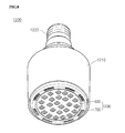
- FIG. 8 is a perspective view showing a lighting unit employing a light emitting device package according to the embodiments.
- each layer shown in the drawings may be exaggerated, omitted or schematically drawn for the purpose of convenience or clarity.
- the size of elements does not utterly reflect an actual size.
- FIG. 1 is a sectional view showing a light emitting device package according to the first embodiment.
- the light emitting device package includes a body 100, first and second electrode layers 110 and 120 formed on the body 100, a light emitting device 200 formed on the body 100 and electrically connected to the first and second electrode layers 110 and 120, a luminescent layer 310 surrounding the light emitting device 200, and an encapsulant layer 320 formed on the luminescent layer 310.
- the body 100 may include silicon, resin or a metallic material.
- the body 100 can be formed therein with a cavity surrounding the light emitting device 200 and having an inclined surface and a reflective layer (not shown) can be formed on the inclined surface.
- the first and second electrode layers 110 and 120 are electrically isolated from each other and extend by passing through the body 100 to supply power to the light emitting device 200.
- the first and second electrode layers 110 and 120 may reflect the light emitted from the light emitting device 200 to improve the light efficiency or dissipate heat generated from the light emitting device 200 to the outside.
- the light emitting device 200 may include a lateral type light emitting device, in which an n-side electrode layer and a p-side electrode layer are formed on a top surface of a light emitting device structure, a flip chip type light emitting device, in which the n-side electrode layer and the p-side electrode layer are formed on a bottom surface of the light emitting device structure, or a vertical type light emitting device, in which the n-side electrode layer and the p-side electrode layer are formed on the top surface and the bottom surface of the light emitting device structure, respectively.
- FIG. 1 a lateral type light emitting device, in which an n-side electrode layer and a p-side electrode layer are formed on a top surface of a light emitting device structure
- a flip chip type light emitting device in which the n-side electrode layer and the p-side electrode layer are formed on a bottom surface of the light emitting device structure
- a vertical type light emitting device in which the n-side electrode layer and the p
- the light emitting device 200 may include an n type semiconductor layer, an active layer and a p type semiconductor layer.
- the light emitting device 200 may be installed on the body 100 or the first or second electrode layer 110 or 120. Referring to FIG. 1 , the light emitting device 200 is installed on the second electrode layer 120.
- the luminescent layer 310 is formed on the body 100 to surround the light emitting device 200, and the encapsulant layer 320 is formed on the luminescent layer 310.
- the luminescent layer 310 converts a color of the light emitted from the light emitting device 200 and the encapsulant layer 320 protects the luminescent layer 310 and serves as a lens to control the orientation angle of the light emitted from the light emitting device 200.
- a top surface of the encapsulant layer 320 is convex.
- the luminescent layer 310 can be formed by distributing luminescence materials into silicon gel or epoxy.
- the luminescence materials may include a silicate, a phosphate, an aluminate, or a sulfide and a transition metal or a rare-earth metal is used at the center of light emission.
- the luminescence materials may be classified into a yellow luminescence material, a red luminescence material and a green luminescence material.
- the encapsulant layer 320 can be formed by distributing high-refractive particles, which have the refractive index higher than that of silicon gel or epoxy, into the silicon gel or the epoxy.
- the refractive index of the luminescent layer 310 matches with the refractive index of the encapsulant layer 320.
- the luminescent layer 310 has a first refractive index and the encapsulant layer 320 has a second refractive index substantially identical to the first refractive index within the deviation of 10%. For instance, if the luminescent layer 310 has the refractive index of 1.7, the encapsulant layer 320 has the refractive index of 1.53 to 1.87.
- the refractive index of the luminescent layer 310 is significantly different from the refractive index of the encapsulant layer 320, the light emitted from the light emitting device 200 may pass through the luminescent layer 310 and then is totally reflected at the boundary between the luminescent layer 310 and the encapsulant layer 320, so that the light may travel back to the luminescent layer 310 before the light is emitted to the outside.
- the luminescent layer 310 has the refractive index identical to or similar to that of the encapsulant layer 320, thereby reducing the color variation of the light emitted from the light emitting device 200.
- the luminescent layer 310 can be formed by mixing the silicon gel having the refractive index of 1.4 to 1.6 with the YAG-based luminescence material having the refractive index of about 1.8 or the silicate-based luminescence material having the refractive index of about 2.0.
- the luminescent layer 310 may have the effective refractive index of about 1.6 to 1.8.
- the encapsulant layer 320 can be formed by using the silicon gel having the refractive index of 1.4 to 1.6. In this case, the amount of the light totally reflected from the boundary between the luminescent layer 310 and the encapsulant layer 320 may increase due to the difference in the refractive index.
- particles are added to the encapsulant layer 320 in such a manner that the encapsulant layer 320 may have the effective refractive index similar to the effective refractive index of the luminescent layer 310.
- the particles may include high-refractive particles.
- the particles may include at least one of metal oxide, TiO 2 , Al 2 O 3 , TaO 2 , CeO 2 and silica. If the particles are added to the encapsulant layer 320, the effective refractive index of the encapsulant layer 320 may increase to 1.44 to 1.98.
- the luminescent layer 310 may have the refractive index identical to or similar to the refractive index of the encapsulant layer 320, so that the total reflection may rarely occur at the boundary between the luminescent layer 310 and the encapsulant layer 320, thereby reducing the color variation of the light emitted from the light emitting device 200.
- FIG. 2 is a sectional view showing a light emitting device package according to the second embodiment.
- the light emitting device package includes a body 100, first and second electrode layers 110 and 120 formed on the body 100, a light emitting device 200 formed on the body 100 and electrically connected to the first and second electrode layers 110 and 120, a luminescent layer 310 surrounding the light emitting device 200, and an encapsulant layer 320 formed on the luminescent layer 310.
- the body 100 has a flat top surface and a reflective layer (not shown) may be formed on the top surface of the body 100.
- a reflective layer (not shown) may be formed on the top surface of the body 100.
- the first and second electrode layers 110 and 120 may serve as the reflective layer.
- the light emitting device 200 may include a flip chip type light emitting device electrically connected to the first and second electrode layers 110 and 120 through first and second bumps 220 and 230.
- the luminescent layer 310 can be formed around the light emitting device 200 with a substantially uniform thickness.
- the luminescent layer 310 can be formed through a conformal coating process.
- the luminescent layer 310 can be prepared as a film including luminescence materials.
- the encapsulant layer 320 may be formed on the luminescent layer 310, the first electrode layer 110 and the second electrode layer 120.
- the luminescent layer 310 Since the luminescent layer 310 is formed through the conformal coating process, the light emitted from the light emitting device 200 may pass through the luminescent layer 310 having the uniform thickness, so that the color variation can be reduced. However, even when the luminescent layer 310 has the uniform thickness, if there is great difference in the refractive index between the luminescent layer 310 and the encapsulant layer 320, some of the light emitted from the light emitting device 200 is totally reflected at the boundary between the luminescent layer 310 and the encapsulant layer 320, so that the light may travel back to the luminescent layer 310 before the light is emitted to the outside. Thus, there is limitation to reduce the color variation of the light emitted from the light emitting device 200 even if the luminescent layer 310 is formed through the conformal coating process.
- the encapsulant layer 320 is formed by distributing high-refractive particles so that the encapsulant layer 320 may have the effective refractive index similar to the effective refractive index of the luminescent layer 310.
- the refractive index of the luminescent layer 310 matches with the refractive index of the encapsulant layer 320, so that the amount of the light totally reflected at the boundary between the luminescent layer 310 and the encapsulant layer 320 may be reduced.
- FIG. 3 is a sectional view showing a light emitting device package according to the third embodiment.
- the light emitting device package includes a body 100, first and second electrode layers 110 and 120 formed on the body 100, a light emitting device 200 formed on the body 100 and electrically connected to the first and second electrode layers 110 and 120, a luminescent layer 310 surrounding the light emitting device 200, and an encapsulant layer 320 formed on the luminescent layer 310.
- the body 100 may include an inclined surface formed around the light emitting device 200 and a reflective layer (not shown) can be formed on the inclined surface.
- the first and second electrode layers 110 and 120 are electrically isolated from each other and extend by passing through the body 100 to supply power to the light emitting device 200.
- the first and second electrode layers 110 and 120 may reflect the light emitted from the light emitting device 200 to improve the light efficiency or dissipate heat generated from the light emitting device 200 to the outside.
- the light emitting device 200 may include a flip chip type light emitting device electrically connected to the first and second electrode layers 110 and 120 through first and second bumps 220 and 230.
- the luminescent layer 310 can be formed around the light emitting device 200 with a substantially uniform thickness.
- the luminescent layer 310 can be formed through a conformal coating process.
- the luminescent layer 310 can be prepared as a film including luminescence materials.
- the encapsulant layer 320 may be formed on the luminescent layer 310, the first electrode layer 110 and the second electrode layer 120.
- the encapsulant layer 320 is formed in the cavity defined in the body 100 and has a flat top surface.
- the encapsulant layer 320 includes particles, the light passing through the encapsulant layer 320 may be scattered at an arbitrary angle even if the encapsulant layer 320 has the flat top surface, so that the amount of the light totally reflected at the boundary between the encapsulant layer 320 and an external air layer can be reduced, thereby improving the light efficiency.
- the refractive index of the luminescent layer 310 matches with the refractive index of the encapsulant layer 320, so that the amount of the light totally reflected at the boundary between the luminescent layer 310 and the encapsulant layer 320 may be reduced.
- the encapsulant layer 320 may be formed by distributing high-refractive particles such that the encapsulant layer 320 may have the effective refractive index similar to the effective refractive index of the luminescent layer 310. Thus, the light passing through the encapsulant layer 320 may be scattered at the arbitrary angle.
- FIG. 4 is a sectional view showing a light emitting device package according to the fourth embodiment.
- the light emitting device package includes a body 120, first and second electrode layers 131 formed on the body 120, a light emitting device 110 formed on the body 120 and electrically connected to the first and second electrode layers 131, a luminescent layer 151 surrounding the light emitting device 110, and an encapsulant layer 150 surrounding the luminescent layer 151.
- the body 120 can be formed therein with a cavity surrounding the light emitting device 110 and having an inclined surface and a reflective layer (not shown) can be formed on the inclined surface.
- the first and second electrode layers 131 are electrically isolated from each other and extend by passing through the body 120 to supply power to the light emitting device 110.
- the light emitting device 100 may be formed on the body 120, the first electrode layer or the second electrode layer 131.
- the luminescent layer 151 may include a first luminescent layer 151a disposed on a top surface and lateral sides of the light emitting device 110 to surround the light emitting device 110, a second luminescent layer 151b disposed on the first luminescent layer 151a corresponding to the top surface and lateral sides of the light emitting device 110 to surround the light emitting device 110, and a third luminescent layer 151c disposed on the second luminescent layer 151b corresponding to the top surface and lateral sides of the light emitting device 110 to surround the light emitting device 110.
- the first to third luminescent layers 151 a to 151c are formed around the light emitting device 110 with a substantially uniform thickness.
- the first to third luminescent layers 151 a to 151c may include at least one selected from the group consisting of oxynitride-based luminescence materials, YAG-based luminescence materials, nitride-based luminescence materials, and silicate-based luminescence materials.
- the encapsulant layer 150 may be formed on the luminescent layer 151, the first electrode layer and the second electrode layer 131.
- the encapsulant layer 150 is formed in the cavity defined in the body 120 and has a flat top surface.
- the encapsulant layer 150 includes particles, the light passing through the encapsulant layer 150 may be scattered at an arbitrary angle even if the encapsulant layer 150 has the flat top surface, so that the amount of the light totally reflected at the boundary between the encapsulant layer 150 and an external air layer can be reduced, thereby improving the light efficiency.
- the refractive index of the luminescent layer 151 matches with the refractive index of the encapsulant layer 150, so that the amount of the light totally reflected at the boundary between the luminescent layer 151 and the encapsulant layer 150 may be reduced.
- FIG. 5 is a section view showing an example of the light emitting device used in the light emitting device package according to the embodiments.
- the light emitting device 110 includes a substrate 10, an undoped semiconductor layer 20 on the substrate 10, a light emitting structure layer formed on the undoped semiconductor layer 20 and having a first conductive semiconductor layer 30, an active layer 40 and a second conductive semiconductor layer 50, a first electrode 60 on the first conductive semiconductor layer 30, and a second electrode 70 on the second conductive semiconductor layer 50.
- a first conductive InGaN/GaN superlattice structure or an InGaN/InGaN superlattice structure 35 may be formed between the first conductive semiconductor layer 30 and the active layer 40.
- a second conductive AlGaN layer 55 can be formed between the second conductive semiconductor layer 50 and the active layer 40.
- the substrate 10 may include at least one of Al 2 O 3 , single crystalline, SiC, GaAs, GaN, ZnO, AlN, Si, GaP, InP and Ge substrates, but the embodiment is not limited thereto.
- the substrate 10 may include a sapphire substrate serving as a growth substrate for the light emitting structure layer.
- a plurality of protrusion patterns 11 may be formed on the substrate 10.
- the protrusion patterns 11 may scatter the light emitted from the active layer 40 to improve the light efficiency.
- the protrusion patterns 11 may have the shape including one of a hemispherical shape, a polygonal shape, a triangular pyramid shape and a nano-column shape.
- the undoped semiconductor layer 20 is not intentionally doped with first conductive impurities, the undoped semiconductor layer 20 is a nitride layer having a first conductive conduction property.
- the undoped semiconductor layer 20 may include an undoped-GaN layer.
- a buffer layer can be formed between the undoped semiconductor layer 20 and the substrate 10.
- the undoped semiconductor layer 20 may be omitted.
- the first conductive semiconductor layer 30 may include an N type semiconductor layer.
- the first conductive semiconductor layer 20 may include a semiconductor material having a compositional formula of In x AI y Ga 1-x-y N (0 ⁇ x ⁇ 1, 0 ⁇ y ⁇ 1, 0 ⁇ x+y ⁇ 1).
- the first conductive semiconductor layer 30 may be selected from the group consisting of InAlGaN, GaN, AlGaN, AlInN, InGaN, AlN, and InN, and may be doped with N type dopant, such as Si, Ge or Sn.
- the active layer 40 emits the light based on the band gap difference of the energy band according to material constituting the active layer 40 through the recombination of electrons (or holes) injected through the first conductive semiconductor layer 30 and holes (or electrons) injected through the second conductive semiconductor layer 50.
- the active layer 40 may have a single quantum well structure, a multiple quantum well (MQW) structure, a quantum dot structure, or a quantum wire structure, but the embodiment is not limited thereto.
- MQW multiple quantum well
- the active layer 40 may include a semiconductor material having a compositional formula of In x Al y Ga 1-x-y N (0 ⁇ x ⁇ 1, 0 ⁇ y ⁇ 1, 0 ⁇ x+y ⁇ 1). If the active layer 40 has the MQW structure, the active layer 40 may have a stack structure of a plurality of well layers and a plurality of barrier layers. For example, the active layer 40 may include a stack structure of InGaN well/GaN barrier layers.
- a clad layer (not shown) doped with N type dopant or P type dopant may be formed on and/or under the active layer 40.
- the clad layer may include an AlGaN layer or an InAlGaN layer.
- the second conductive semiconductor layer 50 may include a P type semiconductor layer.
- the second conductive semiconductor layer 50 may include a semiconductor material having a compositional formula of In x Al y Ga 1-x-y N (0 ⁇ x ⁇ 1, 0 ⁇ y ⁇ 1, 0 ⁇ x+y ⁇ 1).
- the second conductive semiconductor layer 50 may be selected from the group consisting of InAlGaN, GaN, AlGaN, InGaN, AlInN, AlN, and InN.
- the second conductive semiconductor layer 50 may be doped with P type dopant, such as Mg, Zn, Ca, Sr, and Ba.
- the first conductive semiconductor layer 30 may include a P type semiconductor layer
- the second conductive semiconductor layer 50 may include an N type semiconductor layer.
- a third conductive semiconductor layer (not shown) including an N type semiconductor layer or a P type semiconductor layer may be formed on the second conductive semiconductor layer 50.
- the light emitting structure layer may include at least one of an NP, PN, NPN, PNP junction structures.
- the doping concentration of impurities in the first and second conductive semiconductor layers 30 and 50 may be uniform or irregular.
- the light emitting structure layer may have various structures, and the embodiment is not limited thereto.
- the first electrode 60 is disposed on the first conductive semiconductor layer 30 and the second electrode 70 is disposed on the second conductive semiconductor layer 50 to supply power to the active layer 40.
- FIG. 6 is a section view showing another example of the light emitting device used in the light emitting device package according to the embodiments.
- the light emitting device includes a conductive support substrate 80, a light emitting structure layer formed on the conductive support substrate 80 and having a first conductive semiconductor layer 30, an active layer 40 and a second conductive semiconductor layer 50, and a first electrode 60 on the first conductive semiconductor layer 30.
- a first conductive InGaN/GaN superlattice structure or an InGaN/InGaN superlattice structure 35 may be formed between the first conductive semiconductor layer 30 and the active layer 40.
- a second conductive AlGaN layer 55 can be formed between the second conductive semiconductor layer 50 and the active layer 40.
- a light extracting structure 31 prepared in the form of a column or a hole can be formed on the first conductive semiconductor layer 30.
- the light emitted from the active layer 40 can be effectively discharged to the outside due to the light extracting structure 31.
- the light extracting structure 31 may have one of a hemispherical shape, a polygonal shape, a triangular pyramid shape, and a nano-column shape.
- the light extracting structure 31 may include a photonic crystal.
- the conductive support substrate 80 supports the light emitting structure layer and supplies power to the light emitting structure layer together with the first electrode 60.
- the conductive support substrate 80 may include a support layer, a reflective layer and an ohmic contact layer.
- the support layer may include at least one of Cu, Au, Ni, Mo, a Cu-W alloy and a carrier wafer including Si, Ge, GaAs, ZnO or SiC.
- the reflective layer may include a metal, such as Ag or Al.
- the ohmic contact layer may include a material that makes an ohmic contact with respect to the second conductive semiconductor layer 50.
- the ohmic contact layer can be prepared as a single layer or a multiple layer by using at least one selected from the group consisting of ITO (indium tin oxide), IZO (indium zinc oxide), IZTO (indium zinc tin oxide), IAZO (indium aluminum zinc oxide), IGZO (indium gallium zinc oxide), IGTO (indium gallium tin oxide), AZO (aluminum zinc oxide), ATO (antimony tin oxide), GZO (gallium zinc oxide), IrO x , RuO x , RuO x /ITO, Ni, Ag, Ni/IrO x /Au, and Ni/IrO x /Au/ITO.
- the light emitting structure layer may include a plurality of group III to V compound semiconductor layers.
- the first conductive semiconductor layer 30 may include an N type semiconductor layer.
- the first conductive semiconductor layer 20 may include a semiconductor material having a compositional formula of In x Al y Ga 1-a-y N (0 ⁇ x ⁇ 1, 0 ⁇ y ⁇ 1, 0 ⁇ x+y ⁇ 1).
- the first conductive semiconductor layer 30 may be selected from the group consisting of InAlGaN, GaN, AlGaN, AlInN, InGaN, AlN, and InN, and may be doped with N type dopant, such as Si, Ge or Sn.
- the active layer 40 emits the light based on the band gap difference of the energy band according to material constituting the active layer 40 through the recombination of electrons (or holes) injected through the first conductive semiconductor layer 30 and holes (or electrons) injected through the second conductive semiconductor layer 50.
- the active layer 40 may have a single quantum well structure, a multiple quantum well (MQW) structure, a quantum dot structure, or a quantum wire structure, but the embodiment is not limited thereto.
- MQW multiple quantum well
- the active layer 40 may include a semiconductor material having a compositional formula of In x Al y Ga 1-x-y N (0 ⁇ x ⁇ 1, 0 ⁇ y ⁇ 1, 0 ⁇ x+y ⁇ 1). If the active layer 40 has the MQW structure, the active layer 40 may have a stack structure of a plurality of well layers and a plurality of barrier layers. For example, the active layer 40 may include a stack structure of InGaN well/GaN barrier layers.
- a clad layer (not shown) doped with N type dopant or P type dopant may be formed on and/or under the active layer 40.
- the clad layer may include an AlGaN layer or an InAlGaN layer.
- the second conductive semiconductor layer 50 may include a P type semiconductor layer.
- the second conductive semiconductor layer 50 may include a semiconductor material having a compositional formula of In x Al y Ga 1-x-y N (0 ⁇ x ⁇ 1, 0 ⁇ y ⁇ 1, 0 ⁇ x+y ⁇ 1).
- the second conductive semiconductor layer 50 may be selected from the group consisting of InAlGaN, GaN, AlGaN, InGaN, AlInN, AlN, and InN.
- the second conductive semiconductor layer 50 may be doped with P type dopant, such as Mg, Zn, Ca, Sr, and Ba.
- the first conductive semiconductor layer 30 may include a P type semiconductor layer
- the second conductive semiconductor layer 50 may include an N type semiconductor layer.
- a third conductive semiconductor layer (not shown) including an N type semiconductor layer or a P type semiconductor layer may be formed on the second conductive semiconductor layer 50.
- the light emitting structure layer may include at least one of an NP, PN, NPN, PNP junction structures.
- the doping concentration of impurities in the first and second conductive semiconductor layers 30 and 50 may be uniform or irregular.
- the light emitting structure layer may have various structures, and the embodiment is not limited thereto.
- a current blocking area (not shown) is formed between the second conductive semiconductor layer 50 and the conductive support substrate 80 in such a manner that the current blocking area may at least partially overlap with the first electrode 60.
- the current blocking area can be formed by using an electric insulating material or a material having electric conductivity lower than that of the conductive support substrate 80 or can be formed by applying plasma damage to the second conductive semiconductor layer 50.
- the current may be widely spread due to the current blocking layer, so that the light efficiency of the active layer 40 can be improved.
- the effective refractive index of the luminescent layer is identical to or similar to the effective refractive index of the encapsulant layer, so that the color variation of the light emitted from the light emitting device can be effectively reduced.
- a plurality of light emitting device packages according to the embodiments may be arrayed on the substrate, and an optical member including a light guide plate, a prism sheet, a diffusion sheet or a fluorescent sheet may be provided on the optical path of the light emitted from the light emitting device package.
- the light emitting device package, the substrate, and the optical member may serve as a backlight unit or a lighting unit.
- the lighting system may include a backlight unit, a lighting unit, an indicator, a lamp or a streetlamp.
- FIG. 7 is an exploded perspective view showing a backlight unit 1100 employing the light emitting device package according to the embodiments.
- the backlight unit 1100 shown in FIG. 7 is an example of a lighting system and the embodiment is not limited thereto.
- the backlight unit 1100 may include a bottom frame 1140, a light guide member 1120 provided in the bottom frame 1140, and a light emitting module 1110 installed at one side or on the bottom surface of the light guide member 1120.
- a reflective sheet 1130 may be disposed under the light guide member 1120.
- the bottom frame 1140 has a box shape having an open top surface to receive the light guide member 1120, the light emitting module 1110 and the reflective sheet 1130 therein.
- the bottom frame 1140 may include a metallic material or a resin material, but the embodiment is not limited thereto.
- the light emitting module 1110 may include a substrate 700 and a plurality of light emitting device packages 600 mounted on the substrate 700.
- the light emitting device packages 600 can supply light to the light guide member 1120.
- the light emitting module 1110 includes the light emitting device package 600 mounted on the substrate 700 according to the embodiment, the light emitting device 200 may be directly installed in the light emitting module 1110 according to another embodiment.
- the light emitting module 1110 is installed one at least one inner side of the bottom frame 1140 to provide the light to at least one side of the light guide member 1120.
- the light emitting module 1110 can be provided under the bottom frame 1140 to provide the light toward the bottom surface of the light guide member 1120.
- Such an arrangement can be variously changed according to the design of the backlight unit 1100 and the embodiment is not limited thereto.
- the light guide member 1120 is installed in the bottom frame 1140.
- the light guide member 1120 converts the light emitted from the light emitting module 1110 into the surface light to guide the surface light toward a display panel (not shown).
- the light guide member 1120 may include a light guide plate.
- the light guide plate can be manufactured by using acryl-based resin, such as PMMA (polymethyl methacrylate), PET (polyethylene terephthalate), COC, PC (polycarbonate) or PEN (polyethylene naphthalate) resin.
- PMMA polymethyl methacrylate
- PET polyethylene terephthalate
- COC polyethylene terephthalate
- PC polycarbonate
- PEN polyethylene naphthalate
- An optical sheet 1150 may be provided over the light guide member 1120.
- the optical sheet 1150 may include at least one of a diffusion sheet, a light collection sheet, a brightness enhancement sheet, and a fluorescent sheet.
- the optical sheet 1150 has a stack structure of the diffusion sheet, the light collection sheet, the brightness enhancement sheet, and the fluorescent sheet.
- the diffusion sheet 1150 uniformly diffuses the light emitted from the light emitting module 1110 such that the diffused light can be concentrated onto the display panel (not shown) by the light collection sheet.
- the light output from the light collection sheet is randomly polarized and the brightness enhancement sheet increases the degree of polarization of the light output from the light collection sheet.
- the light collection sheet may include a horizontal and/or vertical prism sheet.
- the brightness enhancement sheet may include a dual brightness enhancement film and the fluorescent sheet may include a transmittive plate or a transmittive film including luminescence materials.
- the reflective sheet 1130 can be disposed under the light guide member 1120.
- the reflective sheet 1130 reflects the light, which is emitted through the bottom surface of the light guide member 1120, toward the light exit surface of the light guide member 1120.
- the reflective sheet 1130 may include resin material having a high reflectance, such as PET, PC or PVC resin, but the embodiment is not limited thereto.
- FIG. 8 is a perspective view showing a lighting unit 1200 including the light emitting device package according to the embodiments.
- the lighting unit 1200 shown in FIG. 8 is only one example of the lighting system and the embodiment is not limited thereto.
- the lighting unit 1200 includes a case body 1210, a light emitting module 1230 installed in the case body 1210, and a connection terminal 1220 installed in the case body 1210 to receive power from an external power source.
- the case body 1210 includes material having superior heat dissipation property.
- the case body 1210 includes a metallic material or a resin material.
- the light emitting module 1230 may include the substrate 700 and at least one light emitting device package 600 installed over the substrate 700.
- the light emitting module 1110 includes the light emitting device package 600 mounted on the substrate 700 according to the embodiment, the light emitting device 100 may be directly installed in the light emitting module 1110 according to another embodiment.
- the substrate 700 includes an insulating member printed with a circuit pattern.
- the substrate 700 includes a PCB (printed circuit board), an MC (metal core) PCB, a flexible PCB, or a ceramic PCB.
- the substrate 700 may include a material that effectively reflects the light.
- the surface of the substrate 700 can be coated with a color, such as a white color or a silver color, to effectively reflect the light.
- At least one light emitting device package 600 can be installed on the substrate 700.
- Each light emitting device package 600 may include at least one LED (light emitting diode).
- the LED may include a colored LED that emits the light having the color of red, green, blue or white and a UV (ultraviolet) LED that emits UV light.
- the light emitting module 1230 may have various combinations of light emitting devices to provide various colors and brightness. For instance, the white LED, the red LED and the green LED can be combined to achieve the high color rendering index (CRI).
- a fluorescent sheet can be provided in the path of the light emitted from the light emitting module 1230 to change the wavelength of the light emitted from the light emitting module 1230. For instance, if the light emitted from the light emitting module 1230 has a wavelength band of blue light, the fluorescent sheet may include a yellow luminescence material. In this case, the light emitted from the light emitting module 1230 passes through the fluorescent sheet so that the light is viewed as white light.
- connection terminal 1220 is electrically connected to the light emitting module 1230 to supply power to the light emitting module 1230.
- the connection terminal 1220 has a shape of a socket screw-coupled with the external power source, but the embodiment is not limited thereto.
- the connection terminal 1220 can be prepared in the form of a pin inserted into the external power source or connected to the external power source through a wire.
- At least one of the light guide member, the diffusion sheet, the light collection sheet, the brightness enhancement sheet and the fluorescent sheet is provided in the path of the light emitted from the light emitting module, so that the desired optical effect can be achieved.
- the lighting system includes the light emitting device or the light emitting device package according to the embodiment, so that the light efficiency can be improved.
- any reference in this specification to "one embodiment,” “an embodiment,” “example embodiment,” etc. means that a particular feature, structure, or characteristic described in connection with the embodiment is included in at least one embodiment of the invention.
- the appearances of such phrases in various places in the specification are not necessarily all referring to the same embodiment.
Landscapes
- Led Device Packages (AREA)
- Electroluminescent Light Sources (AREA)
Abstract
Description
- The embodiment relates to a light emitting device package and a lighting system.
- A light emitting diode (LED) is a semiconductor light emitting device that converts current into light. A wavelength of light emitted from the LED may vary depending on a semiconductor material used for manufacturing the LED. This is because the wavelength of the emitted light varies depending on the energy difference between valance band electrons and conduction band electrons, that is, the bandgap of the semiconductor material.
- The LED can generate light having high brightness, so that the LED has been extensively used as a light source for a display device, a vehicle, or a lighting device. In addition, the LED can represent a white color having superior light efficiency by employing luminescence materials or combining LEDs having various colors.
- The embodiment provides a light emitting device package having a novel structure and a lighting system.
- The embodiment provides a light emitting device package capable of emitting light with reduced color variation and a lighting system.
- A light emitting device package according to the embodiment may include a body; first and second electrode layers on the body; a light emitting device electrically connected to the first and second electrode layers on the body; a luminescent layer on the light emitting device; and an encapsulant layer including particles on the luminescent layer, wherein an effective refractive index of the encapsulant layer has a deviation of 10% or less with respect to an effective refractive index of the luminescent layer.
- A lighting system according to the embodiment may include a substrate; and at least one light emitting device package installed on the substrate to serve as a light source, wherein the light emitting device package may include a body; first and second electrode layers on the body; a light emitting device electrically connected to the first and second electrode layers on the body; a luminescent layer on the light emitting device; and an encapsulant layer including particles on the luminescent layer, wherein an effective refractive index of the encapsulant layer has a deviation of 10% or less with respect to an effective refractive index of the luminescent layer.
-
FIG. 1 is a sectional view showing a light emitting device package according to the first embodiment; -
FIG. 2 is a sectional view showing a light emitting device package according to the second embodiment; -
FIG. 3 is a sectional view showing a light emitting device package according to the third embodiment; -
FIG. 4 is a sectional view showing a light emitting device package according to the fourth embodiment; -
FIG. 5 is a section view showing an example of a light emitting device used in a light emitting device package according to the embodiments; -
FIG. 6 is a section view showing another example of a light emitting device used in a light emitting device package according to the embodiments; -
FIG. 7 is an exploded perspective view showing a backlight unit employing a light emitting device package according to the embodiments; and -
FIG. 8 is a perspective view showing a lighting unit employing a light emitting device package according to the embodiments. - In the description of the embodiments, it will be understood that, when a layer (or film), a region, a pattern, or a structure is referred to as being "on" or "under" another substrate, another layer (or film), another region, another pad, or another pattern, it can be "directly" or "indirectly" over the other substrate, layer (or film), region, pad, or pattern, or one or more intervening layers may also be present. Such a position of the layer has been described with reference to the drawings.
- The thickness and size of each layer shown in the drawings may be exaggerated, omitted or schematically drawn for the purpose of convenience or clarity. In addition, the size of elements does not utterly reflect an actual size.
- Hereinafter, a light emitting device package according to embodiments will be described in detail with reference to accompanying drawings.
-
FIG. 1 is a sectional view showing a light emitting device package according to the first embodiment. - Referring to
FIG. 1 , the light emitting device package according to the first embodiment includes abody 100, first andsecond electrode layers body 100, alight emitting device 200 formed on thebody 100 and electrically connected to the first andsecond electrode layers luminescent layer 310 surrounding thelight emitting device 200, and anencapsulant layer 320 formed on theluminescent layer 310. - The
body 100 may include silicon, resin or a metallic material. Thebody 100 can be formed therein with a cavity surrounding thelight emitting device 200 and having an inclined surface and a reflective layer (not shown) can be formed on the inclined surface. - The first and
second electrode layers body 100 to supply power to thelight emitting device 200. In addition, the first andsecond electrode layers light emitting device 200 to improve the light efficiency or dissipate heat generated from thelight emitting device 200 to the outside. - The
light emitting device 200 may include a lateral type light emitting device, in which an n-side electrode layer and a p-side electrode layer are formed on a top surface of a light emitting device structure, a flip chip type light emitting device, in which the n-side electrode layer and the p-side electrode layer are formed on a bottom surface of the light emitting device structure, or a vertical type light emitting device, in which the n-side electrode layer and the p-side electrode layer are formed on the top surface and the bottom surface of the light emitting device structure, respectively.FIG. 1 shows the vertical type light emitting device, in which the n-side electrode layer of thelight emitting device 200 is connected to thefirst electrode layer 110 through awire 210 and the p-side electrode layer is connected to thesecond electrode layer 120. For instance, thelight emitting device 200 may include an n type semiconductor layer, an active layer and a p type semiconductor layer. - The
light emitting device 200 may be installed on thebody 100 or the first orsecond electrode layer FIG. 1 , thelight emitting device 200 is installed on thesecond electrode layer 120. - The
luminescent layer 310 is formed on thebody 100 to surround thelight emitting device 200, and theencapsulant layer 320 is formed on theluminescent layer 310. Theluminescent layer 310 converts a color of the light emitted from thelight emitting device 200 and theencapsulant layer 320 protects theluminescent layer 310 and serves as a lens to control the orientation angle of the light emitted from thelight emitting device 200. A top surface of theencapsulant layer 320 is convex. Thus, when the light is emitted to the outside through theencapsulant layer 320, the amount of the light totally reflected at the boundary between theencapsulant layer 320 and the outside can be reduced. - The
luminescent layer 310 can be formed by distributing luminescence materials into silicon gel or epoxy. The luminescence materials may include a silicate, a phosphate, an aluminate, or a sulfide and a transition metal or a rare-earth metal is used at the center of light emission. The luminescence materials may be classified into a yellow luminescence material, a red luminescence material and a green luminescence material. - The
encapsulant layer 320 can be formed by distributing high-refractive particles, which have the refractive index higher than that of silicon gel or epoxy, into the silicon gel or the epoxy. - According to the embodiment, the refractive index of the
luminescent layer 310 matches with the refractive index of theencapsulant layer 320. In detail, theluminescent layer 310 has a first refractive index and theencapsulant layer 320 has a second refractive index substantially identical to the first refractive index within the deviation of 10%. For instance, if theluminescent layer 310 has the refractive index of 1.7, theencapsulant layer 320 has the refractive index of 1.53 to 1.87. - If the refractive index of the
luminescent layer 310 is significantly different from the refractive index of theencapsulant layer 320, the light emitted from thelight emitting device 200 may pass through theluminescent layer 310 and then is totally reflected at the boundary between theluminescent layer 310 and theencapsulant layer 320, so that the light may travel back to theluminescent layer 310 before the light is emitted to the outside. There is difference of color conversion between the light directly emitted to the outside without being totally reflected at the boundary between theluminescent layer 310 and theencapsulant layer 320 and the light emitted to the outside after being totally reflected at the boundary between theluminescent layer 310 and theencapsulant layer 320, so that the color variation of thelight emitting device 200 may occur. - In this regard, according to the light emitting device package of the embodiment, the
luminescent layer 310 has the refractive index identical to or similar to that of theencapsulant layer 320, thereby reducing the color variation of the light emitted from thelight emitting device 200. - For instance, the
luminescent layer 310 can be formed by mixing the silicon gel having the refractive index of 1.4 to 1.6 with the YAG-based luminescence material having the refractive index of about 1.8 or the silicate-based luminescence material having the refractive index of about 2.0. Theluminescent layer 310 may have the effective refractive index of about 1.6 to 1.8. Meanwhile, theencapsulant layer 320 can be formed by using the silicon gel having the refractive index of 1.4 to 1.6. In this case, the amount of the light totally reflected from the boundary between theluminescent layer 310 and theencapsulant layer 320 may increase due to the difference in the refractive index. - In this regard, according to the embodiment, particles are added to the
encapsulant layer 320 in such a manner that theencapsulant layer 320 may have the effective refractive index similar to the effective refractive index of theluminescent layer 310. - The particles may include high-refractive particles. For instance, the particles may include at least one of metal oxide, TiO2, Al2O3, TaO2, CeO2 and silica. If the particles are added to the
encapsulant layer 320, the effective refractive index of theencapsulant layer 320 may increase to 1.44 to 1.98. - Therefore, the
luminescent layer 310 may have the refractive index identical to or similar to the refractive index of theencapsulant layer 320, so that the total reflection may rarely occur at the boundary between theluminescent layer 310 and theencapsulant layer 320, thereby reducing the color variation of the light emitted from thelight emitting device 200. -
FIG. 2 is a sectional view showing a light emitting device package according to the second embodiment. - In the following description of the second embodiment, details of elements and structures that have been described in the first embodiment will be omitted in order to avoid redundancy.
- Referring to
FIG. 2 , the light emitting device package according to the second embodiment includes abody 100, first andsecond electrode layers body 100, alight emitting device 200 formed on thebody 100 and electrically connected to the first andsecond electrode layers luminescent layer 310 surrounding thelight emitting device 200, and anencapsulant layer 320 formed on theluminescent layer 310. - The
body 100 has a flat top surface and a reflective layer (not shown) may be formed on the top surface of thebody 100. In addition, the first and second electrode layers 110 and 120 may serve as the reflective layer. - The
light emitting device 200 may include a flip chip type light emitting device electrically connected to the first and second electrode layers 110 and 120 through first andsecond bumps - The
luminescent layer 310 can be formed around thelight emitting device 200 with a substantially uniform thickness. In detail, theluminescent layer 310 can be formed through a conformal coating process. In addition, theluminescent layer 310 can be prepared as a film including luminescence materials. - The
encapsulant layer 320 may be formed on theluminescent layer 310, thefirst electrode layer 110 and thesecond electrode layer 120. - Since the
luminescent layer 310 is formed through the conformal coating process, the light emitted from thelight emitting device 200 may pass through theluminescent layer 310 having the uniform thickness, so that the color variation can be reduced. However, even when theluminescent layer 310 has the uniform thickness, if there is great difference in the refractive index between theluminescent layer 310 and theencapsulant layer 320, some of the light emitted from thelight emitting device 200 is totally reflected at the boundary between theluminescent layer 310 and theencapsulant layer 320, so that the light may travel back to theluminescent layer 310 before the light is emitted to the outside. Thus, there is limitation to reduce the color variation of the light emitted from thelight emitting device 200 even if theluminescent layer 310 is formed through the conformal coating process. - As described above in the first embodiment, the
encapsulant layer 320 is formed by distributing high-refractive particles so that theencapsulant layer 320 may have the effective refractive index similar to the effective refractive index of theluminescent layer 310. - In addition, according to the light emitting device package of the embodiment, the refractive index of the
luminescent layer 310 matches with the refractive index of theencapsulant layer 320, so that the amount of the light totally reflected at the boundary between theluminescent layer 310 and theencapsulant layer 320 may be reduced. -
FIG. 3 is a sectional view showing a light emitting device package according to the third embodiment. - In the following description of the third embodiment, details of elements and structures that have been described in the first and second embodiments will be omitted in order to avoid redundancy.
- Referring to
FIG. 3 , the light emitting device package according to the third embodiment includes abody 100, first and second electrode layers 110 and 120 formed on thebody 100, alight emitting device 200 formed on thebody 100 and electrically connected to the first and second electrode layers 110 and 120, aluminescent layer 310 surrounding thelight emitting device 200, and anencapsulant layer 320 formed on theluminescent layer 310. - The
body 100 may include an inclined surface formed around thelight emitting device 200 and a reflective layer (not shown) can be formed on the inclined surface. - The first and second electrode layers 110 and 120 are electrically isolated from each other and extend by passing through the
body 100 to supply power to thelight emitting device 200. In addition, the first and second electrode layers 110 and 120 may reflect the light emitted from thelight emitting device 200 to improve the light efficiency or dissipate heat generated from thelight emitting device 200 to the outside. - The
light emitting device 200 may include a flip chip type light emitting device electrically connected to the first and second electrode layers 110 and 120 through first andsecond bumps - The
luminescent layer 310 can be formed around thelight emitting device 200 with a substantially uniform thickness. In detail, theluminescent layer 310 can be formed through a conformal coating process. In addition, theluminescent layer 310 can be prepared as a film including luminescence materials. - The
encapsulant layer 320 may be formed on theluminescent layer 310, thefirst electrode layer 110 and thesecond electrode layer 120. Theencapsulant layer 320 is formed in the cavity defined in thebody 100 and has a flat top surface. - Since the
encapsulant layer 320 includes particles, the light passing through theencapsulant layer 320 may be scattered at an arbitrary angle even if theencapsulant layer 320 has the flat top surface, so that the amount of the light totally reflected at the boundary between theencapsulant layer 320 and an external air layer can be reduced, thereby improving the light efficiency. - Similar to the previous embodiments, according to the light emitting device package of the third embodiment, the refractive index of the
luminescent layer 310 matches with the refractive index of theencapsulant layer 320, so that the amount of the light totally reflected at the boundary between theluminescent layer 310 and theencapsulant layer 320 may be reduced. - The
encapsulant layer 320 may be formed by distributing high-refractive particles such that theencapsulant layer 320 may have the effective refractive index similar to the effective refractive index of theluminescent layer 310. Thus, the light passing through theencapsulant layer 320 may be scattered at the arbitrary angle. -
FIG. 4 is a sectional view showing a light emitting device package according to the fourth embodiment. - In the following description of the fourth embodiment, details of elements and structures that have been described in the first to third embodiments will be omitted in order to avoid redundancy.
- Referring to
FIG. 4 , the light emitting device package according to the fourth embodiment includes abody 120, first and second electrode layers 131 formed on thebody 120, alight emitting device 110 formed on thebody 120 and electrically connected to the first and second electrode layers 131, a luminescent layer 151 surrounding thelight emitting device 110, and anencapsulant layer 150 surrounding the luminescent layer 151. - The
body 120 can be formed therein with a cavity surrounding thelight emitting device 110 and having an inclined surface and a reflective layer (not shown) can be formed on the inclined surface. - The first and second electrode layers 131 are electrically isolated from each other and extend by passing through the
body 120 to supply power to thelight emitting device 110. - The
light emitting device 100 may be formed on thebody 120, the first electrode layer or thesecond electrode layer 131. - The luminescent layer 151 may include a first
luminescent layer 151a disposed on a top surface and lateral sides of thelight emitting device 110 to surround thelight emitting device 110, a secondluminescent layer 151b disposed on the firstluminescent layer 151a corresponding to the top surface and lateral sides of thelight emitting device 110 to surround thelight emitting device 110, and a thirdluminescent layer 151c disposed on the secondluminescent layer 151b corresponding to the top surface and lateral sides of thelight emitting device 110 to surround thelight emitting device 110. The first to thirdluminescent layers 151 a to 151c are formed around thelight emitting device 110 with a substantially uniform thickness. In addition, the first to thirdluminescent layers 151 a to 151c may include at least one selected from the group consisting of oxynitride-based luminescence materials, YAG-based luminescence materials, nitride-based luminescence materials, and silicate-based luminescence materials. - The
encapsulant layer 150 may be formed on the luminescent layer 151, the first electrode layer and thesecond electrode layer 131. Theencapsulant layer 150 is formed in the cavity defined in thebody 120 and has a flat top surface. - Since the
encapsulant layer 150 includes particles, the light passing through theencapsulant layer 150 may be scattered at an arbitrary angle even if theencapsulant layer 150 has the flat top surface, so that the amount of the light totally reflected at the boundary between theencapsulant layer 150 and an external air layer can be reduced, thereby improving the light efficiency. - Similar to the previous embodiments, according to the light emitting device package of the fourth embodiment, the refractive index of the luminescent layer 151 matches with the refractive index of the
encapsulant layer 150, so that the amount of the light totally reflected at the boundary between the luminescent layer 151 and theencapsulant layer 150 may be reduced. -
FIG. 5 is a section view showing an example of the light emitting device used in the light emitting device package according to the embodiments. - Referring to
FIG. 5 , thelight emitting device 110 includes asubstrate 10, anundoped semiconductor layer 20 on thesubstrate 10, a light emitting structure layer formed on theundoped semiconductor layer 20 and having a firstconductive semiconductor layer 30, anactive layer 40 and a secondconductive semiconductor layer 50, afirst electrode 60 on the firstconductive semiconductor layer 30, and asecond electrode 70 on the secondconductive semiconductor layer 50. - In addition, a first conductive InGaN/GaN superlattice structure or an InGaN/
InGaN superlattice structure 35 may be formed between the firstconductive semiconductor layer 30 and theactive layer 40. - Further, a second
conductive AlGaN layer 55 can be formed between the secondconductive semiconductor layer 50 and theactive layer 40. - For instance, the
substrate 10 may include at least one of Al2O3, single crystalline, SiC, GaAs, GaN, ZnO, AlN, Si, GaP, InP and Ge substrates, but the embodiment is not limited thereto. For example, thesubstrate 10 may include a sapphire substrate serving as a growth substrate for the light emitting structure layer. - A plurality of
protrusion patterns 11 may be formed on thesubstrate 10. Theprotrusion patterns 11 may scatter the light emitted from theactive layer 40 to improve the light efficiency. - For instance, the
protrusion patterns 11 may have the shape including one of a hemispherical shape, a polygonal shape, a triangular pyramid shape and a nano-column shape. - Although the
undoped semiconductor layer 20 is not intentionally doped with first conductive impurities, theundoped semiconductor layer 20 is a nitride layer having a first conductive conduction property. For instance, theundoped semiconductor layer 20 may include an undoped-GaN layer. A buffer layer can be formed between theundoped semiconductor layer 20 and thesubstrate 10. In addition, theundoped semiconductor layer 20 may be omitted. - For example, the first
conductive semiconductor layer 30 may include an N type semiconductor layer. The firstconductive semiconductor layer 20 may include a semiconductor material having a compositional formula of InxAIyGa1-x-yN (0≤x≤1, 0 ≤y≤1, 0≤x+y≤1). For example, the firstconductive semiconductor layer 30 may be selected from the group consisting of InAlGaN, GaN, AlGaN, AlInN, InGaN, AlN, and InN, and may be doped with N type dopant, such as Si, Ge or Sn. - The
active layer 40 emits the light based on the band gap difference of the energy band according to material constituting theactive layer 40 through the recombination of electrons (or holes) injected through the firstconductive semiconductor layer 30 and holes (or electrons) injected through the secondconductive semiconductor layer 50. - The
active layer 40 may have a single quantum well structure, a multiple quantum well (MQW) structure, a quantum dot structure, or a quantum wire structure, but the embodiment is not limited thereto. - The
active layer 40 may include a semiconductor material having a compositional formula of InxAlyGa1-x-yN (0≤x≤1, 0≤y≤1, 0≤x+y≤1). If theactive layer 40 has the MQW structure, theactive layer 40 may have a stack structure of a plurality of well layers and a plurality of barrier layers. For example, theactive layer 40 may include a stack structure of InGaN well/GaN barrier layers. - A clad layer (not shown) doped with N type dopant or P type dopant may be formed on and/or under the
active layer 40. The clad layer may include an AlGaN layer or an InAlGaN layer. - For example, the second
conductive semiconductor layer 50 may include a P type semiconductor layer. The secondconductive semiconductor layer 50 may include a semiconductor material having a compositional formula of InxAlyGa1-x-yN (0≤x≤1, 0 ≤y≤1, 0≤x+y≤1). For example, the secondconductive semiconductor layer 50 may be selected from the group consisting of InAlGaN, GaN, AlGaN, InGaN, AlInN, AlN, and InN. The secondconductive semiconductor layer 50 may be doped with P type dopant, such as Mg, Zn, Ca, Sr, and Ba. - Meanwhile, the first
conductive semiconductor layer 30 may include a P type semiconductor layer, and the secondconductive semiconductor layer 50 may include an N type semiconductor layer. In addition, a third conductive semiconductor layer (not shown) including an N type semiconductor layer or a P type semiconductor layer may be formed on the secondconductive semiconductor layer 50. Accordingly, the light emitting structure layer may include at least one of an NP, PN, NPN, PNP junction structures. In addition, the doping concentration of impurities in the first and second conductive semiconductor layers 30 and 50 may be uniform or irregular. In other words, the light emitting structure layer may have various structures, and the embodiment is not limited thereto. - The
first electrode 60 is disposed on the firstconductive semiconductor layer 30 and thesecond electrode 70 is disposed on the secondconductive semiconductor layer 50 to supply power to theactive layer 40. -
FIG. 6 is a section view showing another example of the light emitting device used in the light emitting device package according to the embodiments. - Referring to
FIG. 6 , the light emitting device includes aconductive support substrate 80, a light emitting structure layer formed on theconductive support substrate 80 and having a firstconductive semiconductor layer 30, anactive layer 40 and a secondconductive semiconductor layer 50, and afirst electrode 60 on the firstconductive semiconductor layer 30. - In addition, a first conductive InGaN/GaN superlattice structure or an InGaN/
InGaN superlattice structure 35 may be formed between the firstconductive semiconductor layer 30 and theactive layer 40. - Further, a second
conductive AlGaN layer 55 can be formed between the secondconductive semiconductor layer 50 and theactive layer 40. - In addition, a
light extracting structure 31 prepared in the form of a column or a hole can be formed on the firstconductive semiconductor layer 30. The light emitted from theactive layer 40 can be effectively discharged to the outside due to thelight extracting structure 31. - For example, the
light extracting structure 31 may have one of a hemispherical shape, a polygonal shape, a triangular pyramid shape, and a nano-column shape. Thelight extracting structure 31 may include a photonic crystal. - The
conductive support substrate 80 supports the light emitting structure layer and supplies power to the light emitting structure layer together with thefirst electrode 60. - The
conductive support substrate 80 may include a support layer, a reflective layer and an ohmic contact layer. The support layer may include at least one of Cu, Au, Ni, Mo, a Cu-W alloy and a carrier wafer including Si, Ge, GaAs, ZnO or SiC. - The reflective layer may include a metal, such as Ag or Al. In addition, the ohmic contact layer may include a material that makes an ohmic contact with respect to the second
conductive semiconductor layer 50. For instance, the ohmic contact layer can be prepared as a single layer or a multiple layer by using at least one selected from the group consisting of ITO (indium tin oxide), IZO (indium zinc oxide), IZTO (indium zinc tin oxide), IAZO (indium aluminum zinc oxide), IGZO (indium gallium zinc oxide), IGTO (indium gallium tin oxide), AZO (aluminum zinc oxide), ATO (antimony tin oxide), GZO (gallium zinc oxide), IrOx, RuOx, RuOx/ITO, Ni, Ag, Ni/IrOx/Au, and Ni/IrOx/Au/ITO. - The light emitting structure layer may include a plurality of group III to V compound semiconductor layers.
- For example, the first
conductive semiconductor layer 30 may include an N type semiconductor layer. The firstconductive semiconductor layer 20 may include a semiconductor material having a compositional formula of InxAlyGa1-a-yN (0≤x≤1, 0 ≤y≤1, 0≤x+y≤1). For example, the firstconductive semiconductor layer 30 may be selected from the group consisting of InAlGaN, GaN, AlGaN, AlInN, InGaN, AlN, and InN, and may be doped with N type dopant, such as Si, Ge or Sn. - The
active layer 40 emits the light based on the band gap difference of the energy band according to material constituting theactive layer 40 through the recombination of electrons (or holes) injected through the firstconductive semiconductor layer 30 and holes (or electrons) injected through the secondconductive semiconductor layer 50. - The
active layer 40 may have a single quantum well structure, a multiple quantum well (MQW) structure, a quantum dot structure, or a quantum wire structure, but the embodiment is not limited thereto. - The
active layer 40 may include a semiconductor material having a compositional formula of InxAlyGa1-x-yN (0≤x≤1, 0≤y≤1, 0≤x+y≤1). If theactive layer 40 has the MQW structure, theactive layer 40 may have a stack structure of a plurality of well layers and a plurality of barrier layers. For example, theactive layer 40 may include a stack structure of InGaN well/GaN barrier layers. - A clad layer (not shown) doped with N type dopant or P type dopant may be formed on and/or under the
active layer 40. The clad layer may include an AlGaN layer or an InAlGaN layer. - For example, the second
conductive semiconductor layer 50 may include a P type semiconductor layer. The secondconductive semiconductor layer 50 may include a semiconductor material having a compositional formula of InxAlyGa1-x-yN (0≤x≤1, 0 ≤y≤1, 0≤x+y≤1). For example, the secondconductive semiconductor layer 50 may be selected from the group consisting of InAlGaN, GaN, AlGaN, InGaN, AlInN, AlN, and InN. The secondconductive semiconductor layer 50 may be doped with P type dopant, such as Mg, Zn, Ca, Sr, and Ba. - Meanwhile, the first
conductive semiconductor layer 30 may include a P type semiconductor layer, and the secondconductive semiconductor layer 50 may include an N type semiconductor layer. In addition, a third conductive semiconductor layer (not shown) including an N type semiconductor layer or a P type semiconductor layer may be formed on the secondconductive semiconductor layer 50. Accordingly, the light emitting structure layer may include at least one of an NP, PN, NPN, PNP junction structures. In addition, the doping concentration of impurities in the first and second conductive semiconductor layers 30 and 50 may be uniform or irregular. In other words, the light emitting structure layer may have various structures, and the embodiment is not limited thereto. - In addition, a current blocking area (not shown) is formed between the second
conductive semiconductor layer 50 and theconductive support substrate 80 in such a manner that the current blocking area may at least partially overlap with thefirst electrode 60. The current blocking area can be formed by using an electric insulating material or a material having electric conductivity lower than that of theconductive support substrate 80 or can be formed by applying plasma damage to the secondconductive semiconductor layer 50. The current may be widely spread due to the current blocking layer, so that the light efficiency of theactive layer 40 can be improved. - As described above, according to the light emitting device package of the embodiments, the effective refractive index of the luminescent layer is identical to or similar to the effective refractive index of the encapsulant layer, so that the color variation of the light emitted from the light emitting device can be effectively reduced.
- A plurality of light emitting device packages according to the embodiments may be arrayed on the substrate, and an optical member including a light guide plate, a prism sheet, a diffusion sheet or a fluorescent sheet may be provided on the optical path of the light emitted from the light emitting device package. The light emitting device package, the substrate, and the optical member may serve as a backlight unit or a lighting unit. For instance, the lighting system may include a backlight unit, a lighting unit, an indicator, a lamp or a streetlamp.
-
FIG. 7 is an exploded perspective view showing abacklight unit 1100 employing the light emitting device package according to the embodiments. Thebacklight unit 1100 shown inFIG. 7 is an example of a lighting system and the embodiment is not limited thereto. - Referring to
FIG. 7 , thebacklight unit 1100 may include abottom frame 1140, alight guide member 1120 provided in thebottom frame 1140, and alight emitting module 1110 installed at one side or on the bottom surface of thelight guide member 1120. In addition, areflective sheet 1130 may be disposed under thelight guide member 1120. - The
bottom frame 1140 has a box shape having an open top surface to receive thelight guide member 1120, thelight emitting module 1110 and thereflective sheet 1130 therein. In addition, thebottom frame 1140 may include a metallic material or a resin material, but the embodiment is not limited thereto. - The
light emitting module 1110 may include asubstrate 700 and a plurality of light emitting device packages 600 mounted on thesubstrate 700. The light emitting device packages 600 can supply light to thelight guide member 1120. Although thelight emitting module 1110 includes the light emittingdevice package 600 mounted on thesubstrate 700 according to the embodiment, thelight emitting device 200 may be directly installed in thelight emitting module 1110 according to another embodiment. - As shown in
FIG. 7 , thelight emitting module 1110 is installed one at least one inner side of thebottom frame 1140 to provide the light to at least one side of thelight guide member 1120. - In addition, the
light emitting module 1110 can be provided under thebottom frame 1140 to provide the light toward the bottom surface of thelight guide member 1120. Such an arrangement can be variously changed according to the design of thebacklight unit 1100 and the embodiment is not limited thereto. - The
light guide member 1120 is installed in thebottom frame 1140. Thelight guide member 1120 converts the light emitted from thelight emitting module 1110 into the surface light to guide the surface light toward a display panel (not shown). - The
light guide member 1120 may include a light guide plate. For instance, the light guide plate can be manufactured by using acryl-based resin, such as PMMA (polymethyl methacrylate), PET (polyethylene terephthalate), COC, PC (polycarbonate) or PEN (polyethylene naphthalate) resin. - An
optical sheet 1150 may be provided over thelight guide member 1120. - The
optical sheet 1150 may include at least one of a diffusion sheet, a light collection sheet, a brightness enhancement sheet, and a fluorescent sheet. For instance, theoptical sheet 1150 has a stack structure of the diffusion sheet, the light collection sheet, the brightness enhancement sheet, and the fluorescent sheet. In this case, thediffusion sheet 1150 uniformly diffuses the light emitted from thelight emitting module 1110 such that the diffused light can be concentrated onto the display panel (not shown) by the light collection sheet. The light output from the light collection sheet is randomly polarized and the brightness enhancement sheet increases the degree of polarization of the light output from the light collection sheet. The light collection sheet may include a horizontal and/or vertical prism sheet. In addition, the brightness enhancement sheet may include a dual brightness enhancement film and the fluorescent sheet may include a transmittive plate or a transmittive film including luminescence materials. - The
reflective sheet 1130 can be disposed under thelight guide member 1120. Thereflective sheet 1130 reflects the light, which is emitted through the bottom surface of thelight guide member 1120, toward the light exit surface of thelight guide member 1120. - The
reflective sheet 1130 may include resin material having a high reflectance, such as PET, PC or PVC resin, but the embodiment is not limited thereto. -
FIG. 8 is a perspective view showing alighting unit 1200 including the light emitting device package according to the embodiments. Thelighting unit 1200 shown inFIG. 8 is only one example of the lighting system and the embodiment is not limited thereto. - Referring to
FIG. 8 , thelighting unit 1200 includes acase body 1210, alight emitting module 1230 installed in thecase body 1210, and aconnection terminal 1220 installed in thecase body 1210 to receive power from an external power source. - Preferably, the
case body 1210 includes material having superior heat dissipation property. For instance, thecase body 1210 includes a metallic material or a resin material. - The
light emitting module 1230 may include thesubstrate 700 and at least one light emittingdevice package 600 installed over thesubstrate 700. Although thelight emitting module 1110 includes the light emittingdevice package 600 mounted on thesubstrate 700 according to the embodiment, thelight emitting device 100 may be directly installed in thelight emitting module 1110 according to another embodiment. - The
substrate 700 includes an insulating member printed with a circuit pattern. For instance, thesubstrate 700 includes a PCB (printed circuit board), an MC (metal core) PCB, a flexible PCB, or a ceramic PCB. - In addition, the
substrate 700 may include a material that effectively reflects the light. The surface of thesubstrate 700 can be coated with a color, such as a white color or a silver color, to effectively reflect the light. - At least one light emitting
device package 600 can be installed on thesubstrate 700. Each light emittingdevice package 600 may include at least one LED (light emitting diode). The LED may include a colored LED that emits the light having the color of red, green, blue or white and a UV (ultraviolet) LED that emits UV light. - The
light emitting module 1230 may have various combinations of light emitting devices to provide various colors and brightness. For instance, the white LED, the red LED and the green LED can be combined to achieve the high color rendering index (CRI). In addition, a fluorescent sheet can be provided in the path of the light emitted from thelight emitting module 1230 to change the wavelength of the light emitted from thelight emitting module 1230. For instance, if the light emitted from thelight emitting module 1230 has a wavelength band of blue light, the fluorescent sheet may include a yellow luminescence material. In this case, the light emitted from thelight emitting module 1230 passes through the fluorescent sheet so that the light is viewed as white light. - The
connection terminal 1220 is electrically connected to thelight emitting module 1230 to supply power to thelight emitting module 1230. Referring toFIG. 8 , theconnection terminal 1220 has a shape of a socket screw-coupled with the external power source, but the embodiment is not limited thereto. For instance, theconnection terminal 1220 can be prepared in the form of a pin inserted into the external power source or connected to the external power source through a wire. - According to the lighting system as described above, at least one of the light guide member, the diffusion sheet, the light collection sheet, the brightness enhancement sheet and the fluorescent sheet is provided in the path of the light emitted from the light emitting module, so that the desired optical effect can be achieved.
- As described above, the lighting system includes the light emitting device or the light emitting device package according to the embodiment, so that the light efficiency can be improved.
- Any reference in this specification to "one embodiment," "an embodiment," "example embodiment," etc. , means that a particular feature, structure, or characteristic described in connection with the embodiment is included in at least one embodiment of the invention. The appearances of such phrases in various places in the specification are not necessarily all referring to the same embodiment. Further, when a particular feature, structure, or characteristic is described in connection with any embodiment, it is submitted that it is within the purview of one skilled in the art to affect such feature, structure, or characteristic in connection with other ones of the embodiments.
- Although embodiments have been described with reference to a number of illustrative embodiments thereof, it should be understood that numerous other modifications and embodiments can be devised by those skilled in the art that will fall within the spirit and scope of the principles of this disclosure. More particularly, various variations and modifications are possible in the component parts and/or arrangements of the subject combination arrangement within the scope of the disclosure, the drawings and the appended claims. In addition to variations and modifications in the component parts and/or arrangements, alternative uses will also be apparent to those skilled in the art.
Claims (11)
- A light emitting device package comprising:a body (100);first and second electrode layers (110, 120) on the body (100);a light emitting device (200) electrically connected to the first and second electrode layers (110, 120) on the body (100);a luminescent layer (310) on the light emitting device (200); andan encapsulant layer (320) including particles on the luminescent layer (310),wherein an effective refractive index of the encapsulant layer (320) has a deviation of 10% or less with respect to an effective refractive index of the luminescent layer (310).
- The light emitting device package of claim 1, wherein the particles include metal oxide.
- The light emitting device package of claim 1, wherein the particles include at least one selected from the group consisting of TiO2, Al2O3, TaO2, CeO2 and silica.
- The light emitting device package of claim 1, wherein the luminescent layer (310) is formed on a surface of the light emitting device (200) with a uniform thickness.
- The light emitting device package of claim 1, wherein the luminescent layer (310) includes a plurality of luminescence layers formed by different materials respectively and stacked on a surface of the light emitting device (200) with a uniform thickness.
- The light emitting device package of claim 1, wherein the luminescent layer (310) is prepared as a film including luminescence materials and attached to a surface of the light
- The light emitting device package of claim 1, wherein the encapsulant layer (320) is formed on the luminescent layer (310) and the first and second electrode layers (110, 120).
- The light emitting device package of claim 1, wherein the encapsulant layer (320) has a convex top surface.
- The light emitting device package of claim 1, wherein the encapsulant layer (320) has a flat top surface.
- The light emitting device package of claim 1, wherein the effective refractive index of the luminescent layer (310) is 1.6 to 1.8 and the effective refractive index of the encapsulant layer (320) is 1.44 to 1.98.
- A lighting system employing a light emitting device as a light source, the lighting system comprising:a substrate (10); andat least one light emitting device package (600) claimed in any one of claims 1 to 10 and installed on the substrate (10).
Applications Claiming Priority (1)
| Application Number | Priority Date | Filing Date | Title |
|---|---|---|---|
| KR1020100000486A KR20110080318A (en) | 2010-01-05 | 2010-01-05 | Light emitting device package |
Publications (3)
| Publication Number | Publication Date |
|---|---|
| EP2341563A2 true EP2341563A2 (en) | 2011-07-06 |
| EP2341563A3 EP2341563A3 (en) | 2014-04-16 |
| EP2341563B1 EP2341563B1 (en) | 2017-10-04 |
Family
ID=43837975
Family Applications (1)
| Application Number | Title | Priority Date | Filing Date |
|---|---|---|---|
| EP11150222.5A Not-in-force EP2341563B1 (en) | 2010-01-05 | 2011-01-05 | Light emitting device package and lighting system |
Country Status (4)
| Country | Link |
|---|---|
| US (1) | US8791495B2 (en) |
| EP (1) | EP2341563B1 (en) |
| KR (1) | KR20110080318A (en) |
| CN (1) | CN102122698A (en) |
Families Citing this family (10)
| Publication number | Priority date | Publication date | Assignee | Title |
|---|---|---|---|---|
| KR20120013758A (en) * | 2010-08-06 | 2012-02-15 | 엘지이노텍 주식회사 | Light emitting device package and manufacturing method thereof |
| US9840790B2 (en) | 2012-08-23 | 2017-12-12 | Hexatech, Inc. | Highly transparent aluminum nitride single crystalline layers and devices made therefrom |
| WO2014120637A1 (en) * | 2013-01-29 | 2014-08-07 | Hexatech, Inc. | Optoelectronic devices incorporating single crystalline aluminum nitride substrate |
| KR102225693B1 (en) | 2013-03-14 | 2021-03-12 | 헥사테크, 인크. | Power semiconductor devices incorporating single crystalline aluminum nitride substrate |
| KR102191213B1 (en) * | 2013-04-12 | 2020-12-15 | 서울바이오시스 주식회사 | Uv light emitting device |
| US10770608B2 (en) * | 2013-05-23 | 2020-09-08 | Garmin Switzerland Gmbh | Semi-transparent thin-film photovoltaic mono cell |
| KR102189129B1 (en) * | 2014-06-02 | 2020-12-09 | 엘지이노텍 주식회사 | Light emitting device module |
| JP6552190B2 (en) * | 2014-12-11 | 2019-07-31 | シチズン電子株式会社 | Light emitting device and method of manufacturing light emitting device |
| CN105720173A (en) * | 2014-12-17 | 2016-06-29 | 日东电工株式会社 | Light semiconductor component covered with fluorescent layer and manufacturing method thereof |
| CN115440868A (en) * | 2022-08-15 | 2022-12-06 | 上海应用技术大学 | A solar-like/full-spectrum LED based on single-component full-spectrum phosphor packaging |
Family Cites Families (26)
| Publication number | Priority date | Publication date | Assignee | Title |
|---|---|---|---|---|
| US20040159900A1 (en) | 2003-01-27 | 2004-08-19 | 3M Innovative Properties Company | Phosphor based light sources having front illumination |
| EP1668960A2 (en) | 2003-09-08 | 2006-06-14 | Nanocrystal Lighting Corporation | Light efficient packaging configurations for led lamps using high refractive index encapsulants |
| US7279724B2 (en) * | 2004-02-25 | 2007-10-09 | Philips Lumileds Lighting Company, Llc | Ceramic substrate for a light emitting diode where the substrate incorporates ESD protection |
| JP2005310756A (en) * | 2004-03-26 | 2005-11-04 | Koito Mfg Co Ltd | Light source module and vehicle headlamp |
| US7495325B2 (en) * | 2005-05-05 | 2009-02-24 | Stats Chippac, Ltd. | Optical die-down quad flat non-leaded package |
| WO2007018039A1 (en) * | 2005-08-05 | 2007-02-15 | Matsushita Electric Industrial Co., Ltd. | Semiconductor light-emitting device |
| JP4961887B2 (en) * | 2005-09-07 | 2012-06-27 | 豊田合成株式会社 | Solid state device |
| JP4415972B2 (en) * | 2005-09-22 | 2010-02-17 | ソニー株式会社 | Method for producing metal oxide nanoparticles |
| CN100470860C (en) | 2006-02-15 | 2009-03-18 | 深圳市量子光电子有限公司 | Light-emitted diode |
| JP2007258136A (en) | 2006-03-27 | 2007-10-04 | Nidec Sankyo Corp | Light source body and lighting device |
| TWI418054B (en) * | 2006-08-08 | 2013-12-01 | Lg電子股份有限公司 | Light emitting device package and method of manufacturing the same |
| KR100866879B1 (en) | 2006-12-19 | 2008-11-04 | 엘지전자 주식회사 | Light emitting device package and its manufacturing method |
| TWI318013B (en) * | 2006-09-05 | 2009-12-01 | Epistar Corp | A light emitting device and the manufacture method thereof |
| TWI338380B (en) * | 2006-10-11 | 2011-03-01 | Chuan Yu Hung | Light emitting diode incorporating high refractive index material |
| KR100818518B1 (en) | 2007-03-14 | 2008-03-31 | 삼성전기주식회사 | LED Package |
| CN101369619B (en) | 2007-08-14 | 2011-01-05 | 富士迈半导体精密工业(上海)有限公司 | Surface Mount Type Light Emitting Diode Assembly and Light Emitting Diode Backlight Module |
| US7791093B2 (en) * | 2007-09-04 | 2010-09-07 | Koninklijke Philips Electronics N.V. | LED with particles in encapsulant for increased light extraction and non-yellow off-state color |
| CN101809088B (en) * | 2007-09-25 | 2012-10-24 | 日立化成工业株式会社 | Thermosetting resin composition for light reflection, substrate for mounting optical-semiconductor element using same, method for producing same, and optical-semiconductor device |
| DE102007057812A1 (en) | 2007-11-30 | 2009-06-25 | Schott Ag | LED, has light converter comprising light conversion material for receiving output light and producing converted light, and sol gel glass, where light conversion material and filler are embedded in sol-gel glass |
| CN101459163B (en) | 2007-12-12 | 2011-07-06 | 富士迈半导体精密工业(上海)有限公司 | Light emitting diode |
| CN101465345B (en) * | 2007-12-19 | 2013-01-09 | 富士迈半导体精密工业(上海)有限公司 | Light source device Light source die set and method for manufacturing the light source device |
| JP2009206459A (en) * | 2008-02-29 | 2009-09-10 | Sharp Corp | Color conversion member and light-emitting apparatus using the same |
| US9287469B2 (en) * | 2008-05-02 | 2016-03-15 | Cree, Inc. | Encapsulation for phosphor-converted white light emitting diode |
| US8415692B2 (en) * | 2009-07-06 | 2013-04-09 | Cree, Inc. | LED packages with scattering particle regions |
| JP5659519B2 (en) * | 2009-11-19 | 2015-01-28 | 豊田合成株式会社 | Light emitting device, method for manufacturing light emitting device, method for mounting light emitting device, and light source device |
| JP5707697B2 (en) * | 2009-12-17 | 2015-04-30 | 日亜化学工業株式会社 | Light emitting device |
-
2010
- 2010-01-05 KR KR1020100000486A patent/KR20110080318A/en not_active Ceased
-
2011
- 2011-01-04 US US12/984,369 patent/US8791495B2/en active Active
- 2011-01-05 EP EP11150222.5A patent/EP2341563B1/en not_active Not-in-force
- 2011-01-05 CN CN2011100053151A patent/CN102122698A/en active Pending
Non-Patent Citations (1)
| Title |
|---|
| None |
Also Published As
| Publication number | Publication date |
|---|---|
| EP2341563A3 (en) | 2014-04-16 |
| US8791495B2 (en) | 2014-07-29 |
| EP2341563B1 (en) | 2017-10-04 |
| CN102122698A (en) | 2011-07-13 |
| US20110198643A1 (en) | 2011-08-18 |
| KR20110080318A (en) | 2011-07-13 |
Similar Documents
| Publication | Publication Date | Title |
|---|---|---|
| US10559734B2 (en) | Light emitting device package and light unit including the same | |
| CN102169939B (en) | Light emitting device, light emitting device package, and lighting system | |
| CN102088049B (en) | Luminescent device and the light emitting device package including luminescent device | |
| US8791495B2 (en) | Light emitting device package and lighting system | |
| EP2360749A2 (en) | Light emitting diode, LED package and lighting system incorporating the same | |
| JP2011119739A (en) | Light-emitting apparatus, and method of manufacturing the same | |
| KR20130023668A (en) | Light emitting device, light emitting device package, and light unit | |
| US20130049038A1 (en) | Light emitting device and light emitting device package | |
| CN102088018A (en) | Light emitting device and light emitting device package having the same | |
| US8916899B2 (en) | Light emitting apparatus and lighting system | |
| US8476646B2 (en) | Light emitting device and light emitting device package | |
| KR20120003775A (en) | Light emitting device, light emitting device manufacturing method, light emitting device package, and lighting system | |
| US9029899B2 (en) | Light emitting device and light emitting device package | |
| US8513697B2 (en) | Light emitting device, method of manufacturing the same, light emitting device package, and illumination system | |
| US8809884B2 (en) | Light emitting device including an electrode on a textured surface, light emitting device package and lighting system | |
| CN102208509B (en) | Light emitting device, method for fabricating light emitting device, and light emitting device package | |
| CN102044612A (en) | Light emitting device, method of manufacturing the same, light emitting device package, and lighting system | |
| KR101977279B1 (en) | Light Emitting Diode Package | |
| KR20120074104A (en) | The light emitting apparatus and the lighting system having the same | |
| KR101852566B1 (en) | Light emitting device, light emitting device package, and light unit | |
| KR20130016667A (en) | Light emitting device, light emitting device package, and light unit | |
| KR20130007172A (en) | Light emitting device, light emitting device package, and light unit |
Legal Events
| Date | Code | Title | Description |
|---|---|---|---|
| PUAI | Public reference made under article 153(3) epc to a published international application that has entered the european phase |
Free format text: ORIGINAL CODE: 0009012 |
|
| AK | Designated contracting states |
Kind code of ref document: A2 Designated state(s): AL AT BE BG CH CY CZ DE DK EE ES FI FR GB GR HR HU IE IS IT LI LT LU LV MC MK MT NL NO PL PT RO RS SE SI SK SM TR |
|
| AX | Request for extension of the european patent |
Extension state: BA ME |
|
| PUAL | Search report despatched |
Free format text: ORIGINAL CODE: 0009013 |
|
| AK | Designated contracting states |
Kind code of ref document: A3 Designated state(s): AL AT BE BG CH CY CZ DE DK EE ES FI FR GB GR HR HU IE IS IT LI LT LU LV MC MK MT NL NO PL PT RO RS SE SI SK SM TR |
|
| AX | Request for extension of the european patent |
Extension state: BA ME |
|
| RIC1 | Information provided on ipc code assigned before grant |
Ipc: H01L 25/075 20060101ALN20140313BHEP Ipc: H01L 33/48 20100101ALN20140313BHEP Ipc: H01L 33/50 20100101AFI20140313BHEP Ipc: H01L 33/58 20100101ALN20140313BHEP Ipc: H01L 33/56 20100101ALI20140313BHEP Ipc: H01L 33/20 20100101ALN20140313BHEP Ipc: H01L 33/60 20100101ALN20140313BHEP |
|
| 17P | Request for examination filed |
Effective date: 20140331 |
|
| RBV | Designated contracting states (corrected) |
Designated state(s): AL AT BE BG CH CY CZ DE DK EE ES FI FR GB GR HR HU IE IS IT LI LT LU LV MC MK MT NL NO PL PT RO RS SE SI SK SM TR |
|
| GRAP | Despatch of communication of intention to grant a patent |
Free format text: ORIGINAL CODE: EPIDOSNIGR1 |
|
| RIC1 | Information provided on ipc code assigned before grant |
Ipc: H01L 33/60 20100101ALN20170329BHEP Ipc: H01L 33/48 20100101ALN20170329BHEP Ipc: H01L 33/50 20100101AFI20170329BHEP Ipc: H01L 33/56 20100101ALI20170329BHEP Ipc: H01L 33/54 20100101ALN20170329BHEP |
|
| RAP1 | Party data changed (applicant data changed or rights of an application transferred) |
Owner name: LG INNOTEK CO., LTD. |
|
| INTG | Intention to grant announced |
Effective date: 20170502 |
|
| RIN1 | Information on inventor provided before grant (corrected) |
Inventor name: KIM, GEUN HO |
|
| GRAA | (expected) grant |
Free format text: ORIGINAL CODE: 0009210 |
|
| GRAS | Grant fee paid |
Free format text: ORIGINAL CODE: EPIDOSNIGR3 |
|
| AK | Designated contracting states |
Kind code of ref document: B1 Designated state(s): AL AT BE BG CH CY CZ DE DK EE ES FI FR GB GR HR HU IE IS IT LI LT LU LV MC MK MT NL NO PL PT RO RS SE SI SK SM TR |
|
| REG | Reference to a national code |
Ref country code: GB Ref legal event code: FG4D |
|
| REG | Reference to a national code |
Ref country code: CH Ref legal event code: EP |
|
| REG | Reference to a national code |
Ref country code: AT Ref legal event code: REF Ref document number: 934773 Country of ref document: AT Kind code of ref document: T Effective date: 20171015 |
|
| REG | Reference to a national code |
Ref country code: IE Ref legal event code: FG4D |
|
| REG | Reference to a national code |
Ref country code: DE Ref legal event code: R096 Ref document number: 602011042051 Country of ref document: DE |
|
| REG | Reference to a national code |
Ref country code: NL Ref legal event code: MP Effective date: 20171004 |
|
| REG | Reference to a national code |
Ref country code: LT Ref legal event code: MG4D |
|
| REG | Reference to a national code |
Ref country code: AT Ref legal event code: MK05 Ref document number: 934773 Country of ref document: AT Kind code of ref document: T Effective date: 20171004 |
|
| PG25 | Lapsed in a contracting state [announced via postgrant information from national office to epo] |
Ref country code: NL Free format text: LAPSE BECAUSE OF FAILURE TO SUBMIT A TRANSLATION OF THE DESCRIPTION OR TO PAY THE FEE WITHIN THE PRESCRIBED TIME-LIMIT Effective date: 20171004 |
|
| PG25 | Lapsed in a contracting state [announced via postgrant information from national office to epo] |
Ref country code: ES Free format text: LAPSE BECAUSE OF FAILURE TO SUBMIT A TRANSLATION OF THE DESCRIPTION OR TO PAY THE FEE WITHIN THE PRESCRIBED TIME-LIMIT Effective date: 20171004 Ref country code: FI Free format text: LAPSE BECAUSE OF FAILURE TO SUBMIT A TRANSLATION OF THE DESCRIPTION OR TO PAY THE FEE WITHIN THE PRESCRIBED TIME-LIMIT Effective date: 20171004 Ref country code: LT Free format text: LAPSE BECAUSE OF FAILURE TO SUBMIT A TRANSLATION OF THE DESCRIPTION OR TO PAY THE FEE WITHIN THE PRESCRIBED TIME-LIMIT Effective date: 20171004 Ref country code: SE Free format text: LAPSE BECAUSE OF FAILURE TO SUBMIT A TRANSLATION OF THE DESCRIPTION OR TO PAY THE FEE WITHIN THE PRESCRIBED TIME-LIMIT Effective date: 20171004 Ref country code: NO Free format text: LAPSE BECAUSE OF FAILURE TO SUBMIT A TRANSLATION OF THE DESCRIPTION OR TO PAY THE FEE WITHIN THE PRESCRIBED TIME-LIMIT Effective date: 20180104 |
|
| PG25 | Lapsed in a contracting state [announced via postgrant information from national office to epo] |
Ref country code: IS Free format text: LAPSE BECAUSE OF FAILURE TO SUBMIT A TRANSLATION OF THE DESCRIPTION OR TO PAY THE FEE WITHIN THE PRESCRIBED TIME-LIMIT Effective date: 20180204 Ref country code: RS Free format text: LAPSE BECAUSE OF FAILURE TO SUBMIT A TRANSLATION OF THE DESCRIPTION OR TO PAY THE FEE WITHIN THE PRESCRIBED TIME-LIMIT Effective date: 20171004 Ref country code: HR Free format text: LAPSE BECAUSE OF FAILURE TO SUBMIT A TRANSLATION OF THE DESCRIPTION OR TO PAY THE FEE WITHIN THE PRESCRIBED TIME-LIMIT Effective date: 20171004 Ref country code: LV Free format text: LAPSE BECAUSE OF FAILURE TO SUBMIT A TRANSLATION OF THE DESCRIPTION OR TO PAY THE FEE WITHIN THE PRESCRIBED TIME-LIMIT Effective date: 20171004 Ref country code: GR Free format text: LAPSE BECAUSE OF FAILURE TO SUBMIT A TRANSLATION OF THE DESCRIPTION OR TO PAY THE FEE WITHIN THE PRESCRIBED TIME-LIMIT Effective date: 20180105 Ref country code: AT Free format text: LAPSE BECAUSE OF FAILURE TO SUBMIT A TRANSLATION OF THE DESCRIPTION OR TO PAY THE FEE WITHIN THE PRESCRIBED TIME-LIMIT Effective date: 20171004 Ref country code: BG Free format text: LAPSE BECAUSE OF FAILURE TO SUBMIT A TRANSLATION OF THE DESCRIPTION OR TO PAY THE FEE WITHIN THE PRESCRIBED TIME-LIMIT Effective date: 20180104 |
|
| REG | Reference to a national code |
Ref country code: DE Ref legal event code: R097 Ref document number: 602011042051 Country of ref document: DE |
|
| PG25 | Lapsed in a contracting state [announced via postgrant information from national office to epo] |
Ref country code: SK Free format text: LAPSE BECAUSE OF FAILURE TO SUBMIT A TRANSLATION OF THE DESCRIPTION OR TO PAY THE FEE WITHIN THE PRESCRIBED TIME-LIMIT Effective date: 20171004 Ref country code: EE Free format text: LAPSE BECAUSE OF FAILURE TO SUBMIT A TRANSLATION OF THE DESCRIPTION OR TO PAY THE FEE WITHIN THE PRESCRIBED TIME-LIMIT Effective date: 20171004 Ref country code: DK Free format text: LAPSE BECAUSE OF FAILURE TO SUBMIT A TRANSLATION OF THE DESCRIPTION OR TO PAY THE FEE WITHIN THE PRESCRIBED TIME-LIMIT Effective date: 20171004 Ref country code: CZ Free format text: LAPSE BECAUSE OF FAILURE TO SUBMIT A TRANSLATION OF THE DESCRIPTION OR TO PAY THE FEE WITHIN THE PRESCRIBED TIME-LIMIT Effective date: 20171004 |
|
| PLBE | No opposition filed within time limit |
Free format text: ORIGINAL CODE: 0009261 |
|
| STAA | Information on the status of an ep patent application or granted ep patent |
Free format text: STATUS: NO OPPOSITION FILED WITHIN TIME LIMIT |
|
| PG25 | Lapsed in a contracting state [announced via postgrant information from national office to epo] |
Ref country code: PL Free format text: LAPSE BECAUSE OF FAILURE TO SUBMIT A TRANSLATION OF THE DESCRIPTION OR TO PAY THE FEE WITHIN THE PRESCRIBED TIME-LIMIT Effective date: 20171004 Ref country code: SM Free format text: LAPSE BECAUSE OF FAILURE TO SUBMIT A TRANSLATION OF THE DESCRIPTION OR TO PAY THE FEE WITHIN THE PRESCRIBED TIME-LIMIT Effective date: 20171004 Ref country code: RO Free format text: LAPSE BECAUSE OF FAILURE TO SUBMIT A TRANSLATION OF THE DESCRIPTION OR TO PAY THE FEE WITHIN THE PRESCRIBED TIME-LIMIT Effective date: 20171004 Ref country code: IT Free format text: LAPSE BECAUSE OF FAILURE TO SUBMIT A TRANSLATION OF THE DESCRIPTION OR TO PAY THE FEE WITHIN THE PRESCRIBED TIME-LIMIT Effective date: 20171004 |
|
| REG | Reference to a national code |
Ref country code: CH Ref legal event code: PL |
|
| 26N | No opposition filed |
Effective date: 20180705 |
|
| GBPC | Gb: european patent ceased through non-payment of renewal fee |
Effective date: 20180105 |
|
| PG25 | Lapsed in a contracting state [announced via postgrant information from national office to epo] |
Ref country code: LU Free format text: LAPSE BECAUSE OF NON-PAYMENT OF DUE FEES Effective date: 20180105 Ref country code: FR Free format text: LAPSE BECAUSE OF NON-PAYMENT OF DUE FEES Effective date: 20180131 |
|
| REG | Reference to a national code |
Ref country code: IE Ref legal event code: MM4A |
|
| REG | Reference to a national code |
Ref country code: FR Ref legal event code: ST Effective date: 20180928 |
|
| REG | Reference to a national code |
Ref country code: BE Ref legal event code: MM Effective date: 20180131 |
|
| PG25 | Lapsed in a contracting state [announced via postgrant information from national office to epo] |
Ref country code: BE Free format text: LAPSE BECAUSE OF NON-PAYMENT OF DUE FEES Effective date: 20180131 Ref country code: GB Free format text: LAPSE BECAUSE OF NON-PAYMENT OF DUE FEES Effective date: 20180105 Ref country code: SI Free format text: LAPSE BECAUSE OF FAILURE TO SUBMIT A TRANSLATION OF THE DESCRIPTION OR TO PAY THE FEE WITHIN THE PRESCRIBED TIME-LIMIT Effective date: 20171004 Ref country code: LI Free format text: LAPSE BECAUSE OF NON-PAYMENT OF DUE FEES Effective date: 20180131 Ref country code: CH Free format text: LAPSE BECAUSE OF NON-PAYMENT OF DUE FEES Effective date: 20180131 |
|
| PG25 | Lapsed in a contracting state [announced via postgrant information from national office to epo] |
Ref country code: IE Free format text: LAPSE BECAUSE OF NON-PAYMENT OF DUE FEES Effective date: 20180105 |
|
| PG25 | Lapsed in a contracting state [announced via postgrant information from national office to epo] |
Ref country code: MC Free format text: LAPSE BECAUSE OF FAILURE TO SUBMIT A TRANSLATION OF THE DESCRIPTION OR TO PAY THE FEE WITHIN THE PRESCRIBED TIME-LIMIT Effective date: 20171004 |
|
| PG25 | Lapsed in a contracting state [announced via postgrant information from national office to epo] |
Ref country code: MT Free format text: LAPSE BECAUSE OF NON-PAYMENT OF DUE FEES Effective date: 20180105 |
|
| PG25 | Lapsed in a contracting state [announced via postgrant information from national office to epo] |
Ref country code: TR Free format text: LAPSE BECAUSE OF FAILURE TO SUBMIT A TRANSLATION OF THE DESCRIPTION OR TO PAY THE FEE WITHIN THE PRESCRIBED TIME-LIMIT Effective date: 20171004 |
|
| PG25 | Lapsed in a contracting state [announced via postgrant information from national office to epo] |
Ref country code: PT Free format text: LAPSE BECAUSE OF FAILURE TO SUBMIT A TRANSLATION OF THE DESCRIPTION OR TO PAY THE FEE WITHIN THE PRESCRIBED TIME-LIMIT Effective date: 20171004 Ref country code: HU Free format text: LAPSE BECAUSE OF FAILURE TO SUBMIT A TRANSLATION OF THE DESCRIPTION OR TO PAY THE FEE WITHIN THE PRESCRIBED TIME-LIMIT; INVALID AB INITIO Effective date: 20110105 |
|
| PG25 | Lapsed in a contracting state [announced via postgrant information from national office to epo] |
Ref country code: MK Free format text: LAPSE BECAUSE OF NON-PAYMENT OF DUE FEES Effective date: 20171004 Ref country code: CY Free format text: LAPSE BECAUSE OF FAILURE TO SUBMIT A TRANSLATION OF THE DESCRIPTION OR TO PAY THE FEE WITHIN THE PRESCRIBED TIME-LIMIT Effective date: 20171004 |
|
| PG25 | Lapsed in a contracting state [announced via postgrant information from national office to epo] |
Ref country code: AL Free format text: LAPSE BECAUSE OF FAILURE TO SUBMIT A TRANSLATION OF THE DESCRIPTION OR TO PAY THE FEE WITHIN THE PRESCRIBED TIME-LIMIT Effective date: 20171004 |
|
| REG | Reference to a national code |
Ref country code: DE Ref legal event code: R081 Ref document number: 602011042051 Country of ref document: DE Owner name: SUZHOU LEKIN SEMICONDUCTOR CO. LTD., TAICANG, CN Free format text: FORMER OWNER: LG INNOTEK CO., LTD, SEOUL, KR |
|
| PGFP | Annual fee paid to national office [announced via postgrant information from national office to epo] |
Ref country code: DE Payment date: 20231205 Year of fee payment: 14 |
|
| REG | Reference to a national code |
Ref country code: DE Ref legal event code: R079 Ref document number: 602011042051 Country of ref document: DE Free format text: PREVIOUS MAIN CLASS: H01L0033500000 Ipc: H10H0020851000 |
|
| REG | Reference to a national code |
Ref country code: DE Ref legal event code: R119 Ref document number: 602011042051 Country of ref document: DE |
|
| PG25 | Lapsed in a contracting state [announced via postgrant information from national office to epo] |
Ref country code: DE Free format text: LAPSE BECAUSE OF NON-PAYMENT OF DUE FEES Effective date: 20250801 |