EP2339864A2 - Dispositif d'affichage d'images stéréoscopiques et son procédé de commande - Google Patents
Dispositif d'affichage d'images stéréoscopiques et son procédé de commande Download PDFInfo
- Publication number
- EP2339864A2 EP2339864A2 EP10003189A EP10003189A EP2339864A2 EP 2339864 A2 EP2339864 A2 EP 2339864A2 EP 10003189 A EP10003189 A EP 10003189A EP 10003189 A EP10003189 A EP 10003189A EP 2339864 A2 EP2339864 A2 EP 2339864A2
- Authority
- EP
- European Patent Office
- Prior art keywords
- image data
- eye
- display device
- input
- time
- Prior art date
- Legal status (The legal status is an assumption and is not a legal conclusion. Google has not performed a legal analysis and makes no representation as to the accuracy of the status listed.)
- Granted
Links
Images


Classifications
-
- H—ELECTRICITY
- H04—ELECTRIC COMMUNICATION TECHNIQUE
- H04N—PICTORIAL COMMUNICATION, e.g. TELEVISION
- H04N13/00—Stereoscopic video systems; Multi-view video systems; Details thereof
- H04N13/30—Image reproducers
- H04N13/356—Image reproducers having separate monoscopic and stereoscopic modes
- H04N13/359—Switching between monoscopic and stereoscopic modes
-
- H—ELECTRICITY
- H04—ELECTRIC COMMUNICATION TECHNIQUE
- H04N—PICTORIAL COMMUNICATION, e.g. TELEVISION
- H04N13/00—Stereoscopic video systems; Multi-view video systems; Details thereof
- H04N13/30—Image reproducers
- H04N13/332—Displays for viewing with the aid of special glasses or head-mounted displays [HMD]
- H04N13/341—Displays for viewing with the aid of special glasses or head-mounted displays [HMD] using temporal multiplexing
-
- H—ELECTRICITY
- H04—ELECTRIC COMMUNICATION TECHNIQUE
- H04N—PICTORIAL COMMUNICATION, e.g. TELEVISION
- H04N13/00—Stereoscopic video systems; Multi-view video systems; Details thereof
- H04N13/10—Processing, recording or transmission of stereoscopic or multi-view image signals
- H04N13/106—Processing image signals
- H04N13/144—Processing image signals for flicker reduction
-
- H—ELECTRICITY
- H04—ELECTRIC COMMUNICATION TECHNIQUE
- H04N—PICTORIAL COMMUNICATION, e.g. TELEVISION
- H04N13/00—Stereoscopic video systems; Multi-view video systems; Details thereof
- H04N13/30—Image reproducers
- H04N13/398—Synchronisation thereof; Control thereof
Definitions
- a stereoscopic image display device and a driving method thereof are provided.
- Binocular parallax is the most important factor to allow a person to perceive the stereoscopic effect at a close range. That is, different 2D images are respectively seen by a right eye and a left eye, and if the image seen by the left eye (hereinafter referred to as a "left-eye image”) and the image seen by the right eye (hereinafter referred to as a "right-eye image”) are transmitted to the brain, the left-eye image and the right-eye image are combined by the brain such that the brain perceives a 3D image having depth.
- the typical stereoscopic image display devices using the binocular parallax effect in 3D image displays are typically categorized as stereoscopic schemes using glasses, such as a shutter glasses or polarized glasses, and autostereoscopic schemes in which a lenticular lens or a parallax barrier is disposed between a user and the display device. Autostereoscopic schemes typically operate without the use of special glasses.
- the left-eye image and the right-eye image are sequentially time-separated and continuously output, and the left-eye shutter and the right-eye shutter of the shutter glasses are selectively open or shut such that the left-eye image and the right-eye image are sequentially viewed by the user and a stereoscopic image is displayed.
- the shutter glasses scheme may easily execute a change between a 2D mode and a 3D mode of a display device, and a loss of data in each mode may not be generated.
- the shutter glasses in which the shutter is open or shut is worn such that the luminance of the stereoscopic image display device and the surroundings thereof may be diminished, e.g., the surrounding and display appear dimmed, a flicker generated by an external light source, such as a fluorescent light, may be easily recognized, and tiredness of the eyes of a user may be serious after viewing the display device through the glasses for an extended period.
- An exemplary embodiment of a stereoscopic image display device includes; a display device into which left-eye image data and right-eye image data are alternately input, and a shutter member including a left-eye shutter and a right-eye shutter, wherein the left-eye shutter and the right-eye shutter are opened in at least one of at least a part of an input period for the left-eye image data and at least a part of an input period for the right-eye image data.
- a backlight which receives a first on pulse applied thereto may be further included, and at least a part of the first on pulse may be applied between the input period of the left-eye image data and the input period of the right-eye image data.
- the display device may be input with normal image data
- the backlight may receive at least one second on pulse applied thereto at the input period of the normal image data
- the magnitude of the first on pulse may be larger than the magnitude of the second on pulse
- the backlight may be a light emitting diode ("LED").
- LED light emitting diode
- the magnitude of the first on pulse may be equal to or larger than about 1.5 times the magnitude of the second on pulse.
- the second on pulse may have a duty ratio of less than about 100%.
- one of the left-eye shutter and the right-eye shutter may be closed and the other may be opened in at least a part of the first on pulse.
- the backlight may be turned on after the passage of a first time from a time when the input of the left-eye image data or the right-eye image data is completed.
- the left-eye shutter and the right-eye shutter may respectively further include a liquid crystal material, and the first time may be greater than the response time of the liquid crystal material of the shutter.
- the right-eye shutter may be closed from the time when the input of the left-eye image data is completed before the passage of the first time, and the left-eye shutter may be closed from the time when the input of the right-eye image data is completed before the passage of the first time.
- the backlight may be turned off from the start of the input of the left-eye image data or the right-eye image data after the passage of the second time.
- the display device may further include a liquid crystal material, and the second time may be shorter than the response time of the liquid crystal material of the display device.
- the second time may be less than about 15% of the response time of the liquid crystal material of the display device.
- the right-eye shutter may be opened after the passage of the second time period from the time when the input of the right-eye image data is started
- the left-eye shutter may be opened after the passage of the second time period from the time when the input of the left-eye image data is started before the passage of the second time.
- the right-eye shutter may be opened before the third time from the time when the input of the right-eye image data is started, and the left-eye shutter may be opened before the third time from the time when the input of the left-eye image data is started.
- An exemplary embodiment of a stereoscopic image display device includes; a display device into which normal image data is input, and into which a left-eye image data and a right-eye image data are alternately input, a backlight which receives a first on pulse and at least one second on pulse, and a shutter member including a left-eye shutter and a right-eye shutter, wherein at least a part of the first on pulse occurs between the input period of the left-eye image data and the input period of the right-eye image data, the second on pulse occurs during the input period of the normal image data, and the magnitude of the first on pulse is larger than the magnitude of the second on pulse.
- An exemplary embodiment of a method for driving a stereoscopic image display device including a display device and a shutter member having a left-eye shutter and a right-eye shutter according to the present invention includes; alternately inputting left-eye image data and right-eye image data to the display device, and opening the left-eye shutter and the right-eye shutter during at least a part of the time when the left-eye image data or the right-eye image data is being input to the display device.
- At least a part of the first on pulse may be applied to the backlight between the input period of the left-eye image data and the input period of the right-eye image data.
- the display device may be input with normal image data, at least one second on pulse may be applied to the backlight during the input of the normal image data, and the magnitude of the first on pulse may be equal to or larger than about 1.5 times the magnitude of the second on pulse.
- one of the left-eye shutter and the right-eye shutter may be closed and the other may maintain the opened state during at least a portion of the first on pulse.
- An exemplary embodiment of a method for driving a stereoscopic image display device including a display device and a shutter member having a left-eye shutter and a right-eye shutter according to the present invention includes; inputting normal image data to the display device and alternately inputting left-eye image data and right-eye image data to the display device, applying at least a part of the first on pulse to a backlight between the input period of the left-eye image data and the input period of the right-eye image data to a backlight, and applying at least one second on pulse to the backlight during the input of the normal image data, wherein the magnitude of the first on pulse is larger than the magnitude of the second on pulse.
- the luminance deterioration may be prevented at the stereoscopic image display device and the surrounding area thereof, the flicker by the external light source may be reduced, the tiredness of the eyes due to watching for a long time may be reduced, and the power consumption of the stereoscopic image display device may be reduced.
- first, second, third etc. may be used herein to describe various elements, components, regions, layers and/or sections, these elements, components, regions, layers and/or sections should not be limited by these terms. These terms are only used to distinguish one element, component, region, layer or section from another element, component, region, layer or section. Thus, a first element, component, region, layer or section discussed below could be termed a second element, component, region, layer or section without departing from the teachings of the present invention.
- relative terms such as “lower” or “bottom” and “upper” or “top,” may be used herein to describe one element's relationship to another elements as illustrated in the Figures. It will be understood that relative terms are intended to encompass different orientations of the device in addition to the orientation depicted in the Figures. For example, if the device in one of the figures is turned over, elements described as being on the “lower” side of other elements would then be oriented on “upper” sides of the other elements. The exemplary term “lower”, can therefore, encompasses both an orientation of “lower” and “upper,” depending on the particular orientation of the figure.
- Exemplary embodiments of the present invention are described herein with reference to cross section illustrations that are schematic illustrations of idealized embodiments of the present invention. As such, variations from the shapes of the illustrations as a result, for example, of manufacturing techniques and/or tolerances, are to be expected. Thus, embodiments of the present invention should not be construed as limited to the particular shapes of regions illustrated herein but are to include deviations in shapes that result, for example, from manufacturing. For example, a region illustrated or described as flat may, typically, have rough and/or nonlinear features. Moreover, sharp angles that are illustrated may be rounded. Thus, the regions illustrated in the figures are schematic in nature and their shapes are not intended to illustrate the precise shape of a region and are not intended to limit the scope of the present invention.
- FIG. 1 to FIG. 9 an exemplary embodiment of a stereoscopic image display device according to the present invention will be described with reference to FIG. 1 to FIG. 9 .
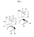
- FIG. 1 is a schematic diagram showing an exemplary embodiment of an operation of an exemplary embodiment of a stereoscopic image display device according to the present invention
- FIG. 9 is a schematic diagram showing an exemplary embodiment of an display apparatus which display a stereoscopic image according to an exemplary embodiment of the present invention.
- FIG. 2 to FIG. 5 are graphs showing a signal waveform of the exemplary embodiment of a stereoscopic image display device of FIG. 1
- FIG. 6 and FIG. 7 are graphs showing a current characteristic of a light-emitting diode (“LED")
- FIG. 8 is a block diagram of an LED driving method in a 2D mode and a 3D mode.
- LED light-emitting diode
- the display device 100 may include a liquid crystal display ("LCD”), an organic light emitting device or other similar display device.
- LCD liquid crystal display
- OLED organic light emitting device
- the following detailed description will describe an exemplary embodiment wherein the display device 100 is an LCD and will be described with reference to FIG. 1 ; however, alternative exemplary embodiments may include configurations wherein the display device 100 is another type of display device as described above.
- the display device 100 may include an upper substrate, a lower substrate and a liquid crystal layer interposed between the upper substrate and the lower substrate.
- the alignment direction of liquid crystal molecules in the liquid crystal layer is controlled by an electric field generated between two electrodes, and thereby the transmittance of light through the liquid crystal layer is controlled so as to display images.
- the lower substrate includes a gate line(GL1,...GLn, in FIG.9 ), a data line(DL1,...DLm, in FIG.9 ), a pixel electrode and a thin film transistor(105 in FIG.9 ) connected thereto.
- the thin film transistor(105 in FIG.9 ) controls the voltage applied to the pixel electrode based on signals applied to the gate line and the data line.
- the pixel electrode may be a transflective pixel electrode including a transmissive region and a reflective region.
- exemplary embodiments include configurations wherein a storage capacitance capacitor(107 in FIG.9 ) may be added, thereby maintaining the voltage applied to the pixel electrode for a predetermined time.
- Exemplary embodiments include configurations wherein the upper substrate corresponding to the lower substrate may include a black matrix, a color filter and a common electrode. Also, alternative exemplary embodiments include configurations wherein at least one of the color filter, the black matrix, and the common electrode may be formed on the lower substrate, and in the exemplary embodiment wherein both the common electrode and the pixel electrode are formed in the lower substrate, at least one of the two electrodes may be a linear electrode.
- the liquid crystal layer may include twisted nematic ("TN”) mode liquid crystals, vertically aligned (“VA”) mode liquid crystals, or electrically controlled birefringence (“ECB”) mode liquid crystals.
- TN twisted nematic
- VA vertically aligned
- EBC electrically controlled birefringence
- Embodiments include configurations wherein polarizers are respectively attached on the outer surfaces of the upper substrate and the lower substrate. Also, embodiments include configurations wherein a compensation film may be added between the substrate and the polarizer.
- the LCD display may include a backlight unit(200 in FIG.9 ).
- the backlight unit(200 in FIG.9 ) includes a light source, examples of which include a fluorescent lamp, such as a cold cathode fluorescent lamp (“CCFL"), and an LED, etc.
- CCFL cold cathode fluorescent lamp
- embodiments also include configurations wherein the backlight unit may additionally include a reflector, a light guide and a luminance improvement film.
- FIG. 9 is a schematic diagram showing an exemplary embodiment of an display apparatus which display a stereoscopic image according to an exemplary embodiment of the present invention.
- the display apparatus 50 includes display device 100, backlight 200, source driver 140, gate driver 120, image signal processor 160, gamma voltage generator 190, luminance controller 210, shutter glasses 300, stereo controller 400, and etc.
- the stereo controller 400 may transmit a 3D timing signal and 3D_EN(3D_enable) to the luminance controller 210.
- the luminance controller 210 may transmit a backlight control signal to the backlight unit 200.
- the backlight unit 200 may turn on or turn off by the backlight control signal through the luminance controller 210 and the stereo controller 400. Backlight control signals transmit to the backlight unit 200 will be explained below with FIG. 2 to FIG. 8 .
- the stereo controller may transmit 3D_sync signal to the shutter glasses 300.
- the shutter glasses may be electrically connected to the stereo controller 400 and the shutter glasses may receive the signal though infra red signal without wire.
- Shutter glasses may be operated in response to the 3D_syn or in response to a transformation of the 3D_sync.
- the 3D_sync may include signals which open or close the shutters.
- shutter glasses control signal(3D_sync) which control the shutter glasses' open or close state will be explained below with FIG. 1 to FIG. 8 .
- the stereo controller may transmit the display DATA to the image signal processor.
- Image signal processor may transmit a various display data and a various control signal to the display device 100 through gate driver 120, data driver 140, a gamma voltage generator 190 or etc. to display image in display device 100.
- the DATA to the image signal processor may include left-eye image and right eye image. image data which is input to the display device 100 will be explained below with FIG. 1 to FIG. 8 .
- the stereoscopic image display device may include a shutter member 300.
- the shutter member 300 may be a glasses-type shutter member 300 as illustrated in FIG. 1 , but the present invention is not limited to a glasses-type shutter member 300.
- the shutter member 300 are formed with right-eye shutters 302 and 302' and left-eye shutters 301 and 301' to alternately block light with a predetermined time period in concert with, e.g., in coordination with, the display device 100.
- the right-eye shutter may be in a closed state 302 or in an open state 302' and the left-eye shutter may be in an open state 301 or in a closed state 301'.
- Both the right-eye shutter and the left-eye shutter may be in an open state. Both the right-eye shutter and the left-eye shutter may be in a closed state.
- the display device 100 may include an infrared emitting member (not shown) and the shutter member 300 may include an infrared receiving member (not shown) for receiving infrared signals from the infrared emitting member.
- the infrared emitting member and the infrared receiving member in communication with each other to drive the shutter member 300.
- the shutter member 300 may include LCDs for each of the left-eye shutter and the right-eye shutter, but the present invention is not limited to the use of an LCD.
- the shutter of the shutter member 300 includes two transparent conductive layers and a liquid crystal layer interposed therebetween, and a polarization film may be disposed on a surface of each conductive layer.
- An orientation of the liquid crystal material is controlled by a voltage applied to the shutter, and the shutter may be closed or opened by the orientation control of the liquid crystal material.
- the left-eye shutter 301 of the shutter member 300 is in the opened state such that the light is transmitted therethrough, and the right-eye shutter 302 is in the closed state such that the light is blocked thereby.
- the right-eye shutter 302' of the shutter member 300 is in the opened state such that the light is transmitted therethrough, and the left-eye shutter 301' is in the closed state such that the light is blocked thereby.
- the left-eye image is perceived by the left eye during the predetermined time and then subsequently the right-eye image is perceived by the right eye, and as a result a stereoscopic image having depth is perceived by a viewer due to the difference between the left-eye image and the right-eye image.
- the image recognized by the left eye is the image displayed at the N-th frame (F(N)), that is, the image in which the quadrangle 101 and the triangle 102 are separated from each other by the distance ⁇ .
- the image recognized by the right eye is the image displayed at the (N+1)-th frame (F(N+1), that is, the image in which the quadrangle 101' and the triangle 102' are separated from each other by the distance ⁇ , which in the present embodiment is different than the distance ⁇ .
- a different distance perception is generated for the quadrilateral and the triangle such that it is perceived by the viewer that the triangle is separated behind the quadrangle, and thereby the viewer experiences depth perception.
- the depth perception in which two objects are separated from each other may be controlled by controlling the distances ⁇ and ⁇ at which the triangle 102 and the quadrilateral 101 are separated from each other.
- the arrow direction shown in the display device 100 represents the sequence through which the gate-on voltage is applied to the gate line(GL1 to GLn, in FIG.9 ). That is, the gate-on voltage may be sequentially applied from the uppermost gate line of the display device 100 to the lowest gate line, e.g., the gate-on voltage is sequentially applied from a gate line corresponding to the top of the display through the gate lines to the gate line corresponding to the bottom of the display.
- the display device 100 may display the left-eye image 101 and 102 as described in more detail below.
- the gate-on voltage is sequentially applied to the gate lines such that the data voltage is applied to the pixel electrodes through the thin film transistors connected to the corresponding gate line.
- the applied data voltage is a data voltage (hereinafter referred to as a left-eye data voltage) to represent the left-eye images 101 and 102, and the applied left-eye data voltage may be maintained during the predetermined time by the storage capacitance of the storage capacitor, where present.
- a data voltage (hereinafter referred to as the right-eye data voltage) to represent the right-eye images 101' and 102' is applied through the same method, and may be maintained during the predetermined time by the storage capacitance of the storage capacitor, where present.
- the left-eye image data L1, L2,... and the right-eye image data R1,... are alternately input to the display device 100; as used herein the term "input to the display device 100" refers to a time period during which the gate ON signals are applied to the gate lines of the display, i.e., a vertical period, and the data voltages corresponding to the sequential gate lines are applied to the corresponding pixel electrodes.
- the left-eye image data and the right eye image data may actually be input to the display 100.
- L1 input period a left-eye image data is drawn(scanned) in the display device 100, and then, in a vertical blanking time threre is no data input to the display device.
- R1 input period a right-eye image data is drawn(scanned) in the display device 100, and then, in a vertical blanking time threre is no data input to the display device.
- a frame may include a data input period and vertical blanking period.
- the image data means data represented as a digital type to output the image to the display device 100.
- FIG. 2 there is a time during which the image data is not input.
- the time period during which the image data is not input occurs before the right-eye image data is input but after the left-eye image data is input.
- the time period during which the image data is not input also occurs before the left-eye image data is input but after the right-eye image data is input.
- the time period during which the image data is not input is referred to as a vertical blanking ("VB") time.
- VB vertical blanking
- one of the left-eye shutters 301 and 301' and the right-eye shutters 302 and 302' is changed to a closed state CLOSE, and the other maintains the opened state OPEN.
- the left-eye shutters 301 and 301' and the right-eye shutters 302 and 302' of the shutter member 300 all are opened during at least a part of the time when the left-eye image data or the right-eye image data is being input.
- image data L1 is input to the display device 100, left -eye shutter and right eye shutter are in an open state.
- right-eye shutter In a vertical blanking(VB) time followed by the L1 period, right-eye shutter is in a closed state and left-eye shutter is in an open state. When image data R1 is input to the display device 100, left-eye shutter and right-eye shutter are in an open state. In a vertical blanking(VB) time followed by the R1 period, right-eye shutter is in an open state and left-eye shutter is in a close state.
- the luminance near the display device 100 may be increased, the display device 100 may itself be bright, the tiredness of the eye may be reduced even when the viewer watches the display device with the shutter member for a long time, and the flicker generated by the external light source may be reduced due to the shorter period where the image is blocked by a closed eye shutter.
- the luminance near the display device 100 is about 162 nit compared to a comparative display device which has a brightness of about 13.5 nit as described below.
- the luminance near the display device is reduced, the display device itself may be dark, the flicker generated by the external light source may be easily recognized, and the tiredness of the eyes may be serious when watching for an extended time period.
- the luminance of the display device is only about 13.5 nit as mentioned above.
- the backlight is turned on during at least a part of time among the VB, and is turned off during most of the time when the left-eye image data or the right-eye image data is input, and accordingly the power consumption of the display device 100 may be reduced.
- the backlight may remain turned on during a brief time period where the subsequent image data is being inputted, e.g., time period t2 to be described in more detail below.
- the opened right-eye shutter 302 is changed to the closed state, the opened left-eye shutter 301 maintains the opened state and the backlight is turned on, and thereby the left-eye image, including the quadrilateral 101 and the triangle 102, output to the display device 100 is shown through the left-eye shutter 301 and perceived by a viewer.
- the closed right-eye shutter 302 is opened (albeit after a small delay corresponding to time period t2), and the left-eye shutter 301 maintains the opened state.
- the opened left-eye shutter 301 is changed to the closed state
- the opened right-eye shutter 302' maintains the opened state and the backlight unit is turned on, and thereby the right-eye image, including the quadrilateral 101' and the triangle 102', output to the display device 100 are shown through the right-eye shutter 302'.
- the backlight may be turned on after a predetermined time t1 after the time when the input of the left-eye image data or the right-eye image data is completed.
- the time t1 may be a sufficient time for the left-eye shutter or the right-eye shutter to be completely closed. That is, when considering the response time of the liquid crystal molecules inside the shutter, the shutter may be previously applied with the voltage before the backlight is turned on during the VB period. Accordingly, the image is shown through the shutter of the other side after the shutter of one side is completely closed such that cross-talk in which the left-eye image and the right-eye image are overlapped may be substantially reduced or effectively prevented.
- the response time of the liquid crystal molecules inside the shutter is changed by the influence of the ambient temperature and the application voltage such that the time t1 may be automatically or manually controlled when the response time of the liquid crystal becomes slower or faster.
- the time t1 may be a sufficient time for the left-eye shutter or the right-eye shutter to be completely closed.
- the time t1 may be controlled to increase the luminance of the display device while reducing the perceived cross-talk.
- the time t1 may be larger than the closing time of the shutter liquid crystal and may be smaller than the entire VB period.
- the falling time (corresponding to the closing time) of the liquid crystal is about 0.3 ms and the VB is about 2.65 ms
- the time t1 may be larger than about 0.3 ms and less than about 2.65 ms.
- exemplary embodiments include configurations wherein the time t1 may be larger than 0.5 ms and less than 2.0 ms.
- the backlight may maintain the opened state during the time t2.
- the luminance of the display device 100 is increased as the time when the backlight is turned on is increased such that the luminance of the display device 100 may be increased when the time t2 is larger than 0 ms.
- the response speed of the liquid crystal of the display device 100 is slow during the initial time when the left-eye image data or the right-eye image data is started to be input such that the cross-talk may not be generated although the backlight is turned on.
- the response time of the liquid crystal inside the display device 100 is changed by the influence of the ambient temperature and the application voltage such that the time t2 may be automatically or manually controlled when the response time of the liquid crystal become slower or faster.
- the time t2 may be 0 ms.
- the backlight is changed to the off state at the moment that the left-eye image data or the right-eye image data is input.
- the cross-talk and the luminance of the display device have a trade-off relationship according to the size of the time t2.
- the time t2 may be controlled to increase the luminance of the display device while reducing the cross-talk.
- the time t2 may be more than 0, and may be less than about 15% of the rising time of the liquid crystal of the display device.
- the time t2 may be more than 0 and less than about 0.6 ms. Furthermore, in one exemplary embodiment the time t2 may be more than 0.1 ms and less than 0.5 ms.
- the time when the closed shutter is changed to the opened state may be substantially the same as the time when the backlight is turned-off, and accordingly the cross-talk may be prevented.
- the shutter is changed from the closed state to the opened state at the time when the backlight is turned off.
- the shutter is changed from the closed state to the opened state at the time when the backlight is turned off.
- the time when the closed shutter is changed to the opened state may be before the time when the left-eye image data or the right-eye image data is input. Accordingly, the time when the shutter is opened is further increased such that the luminance near the display device 100 may be increased.
- the time t3 is less than the response speed of the shutter liquid crystal, and is a short time in which the right-eye is not capable of recognizing the left-eye image and thus cross-talk may be reduced or effectively prevented.
- the response time of the liquid crystal of the display device 100 and the response time of the liquid crystal of the shutter member 300 are exemplarily shown.
- the data response of the liquid crystal for the left-eye image data L1 input to the pixel row of the lower portion of the display device 100 and the data response of the liquid crystal for the right-eye image data R1 input to the pixel row of the upper portion of the display device 100 may be slower than the response of the liquid crystal of the shutter member 300.
- the response time r1 of the display device 100 may be about 4 ms
- the rising(closing) time r2 of the liquid crystal of the shutter member 300 may be about 0.3 ms
- the falling time r3 (corresponding to the opening time) of the liquid crystal of the shutter member 300 may be about 1.38 ms
- the VB period may be about 2.65 ms.
- the luminance of the backlight in the 3D mode may be higher than the luminance of the backlight in the 2D mode. That is, the luminance when the backlight in the 3D mode is in the ON state may be higher than the luminance when the backlight in the 2D mode is in the ON state.
- Driving the backlight by controlling the magnitude of the voltage applied thereto at the special period corresponding to the 3D mode ON state is referred to as impulsive driving. Accordingly, the luminance of the display device 100 in the 3D mode may be increased.
- One method for impulse driving includes having the magnitude i1 of the ON pulse of the backlight in the 3D mode be larger than the magnitude i2 of the ON pulse of the backlight of the 2D mode.
- the magnitude i1 of the ON pulse of the backlight in the 3D mode may be larger than the magnitude i2 of the ON pulse of the backlight of the 2D mode in the range of about 1.5 to about 2 times or more.
- the backlight may be driven by applying a current of about 20 mA in the 2D mode and the backlight may be driven by applying a current of about 30-40 mA in the 3D mode.
- the 2D mode may be a state in which the shutter member is not worn (such a situation is similar to the state in which the left-eye shutter and the right-eye shutter are always opened), and the backlight may be continuously turned on during the time when the image data D1 is input (a duty ratio may be about 100%).
- the duty ratio of the backlight in the 2D mode may be controlled by pulse width modulation ("PWM"), and in such an exemplary embodiment the time when the backlight is turned on is decreased such that the power consumption may be reduced.
- PWM pulse width modulation
- the duty ratio ((a1+a2)/(a1+a2+b1+b2)) may be less than about 100%, and in one exemplary embodiment may be about 50%. In another exemplary embodiment the duty ratio may be about 30%.
- a1 and a2 refer to the time period when the backlight is applied with the voltage
- b1 and b2 refer to the time when the backlight is not applied with the voltage.
- FIG. 6 and FIG. 7 are graphs showing a characteristic of a current ON/OFF of the LED of the backlight.
- the LED has a very high current response speed such that the current response speed may be represented as a nanosecond unit under the conversion from the ON state to the OFF state (or from the OFF state to the ON state).
- the interval of one line of the time axis of FIG. 6 is about 20 ns, and the line interval of the current axis is about 1 V.
- the interval of one line of the time axis of FIG. 7 is about 40 ns, and the line interval of the current axis is about 1 V.
- the time when the LED of the OFF state reaches the ON state by applying the voltage may be about 32.4 ns. It may be confirmed that this response speed of the LED is very fast compared with the response speed of the liquid crystal having a millisecond unit of time measurement, e.g., the LED responds on the nanosecond time scale whereas the liquid crystal has a response speed on the millisecond time scale.
- FIG. 7 shows the time when the LED of the ON state is changed to the OFF state. As shown in FIG. 7 , the time when the LED of the ON state is changed into the OFF state is about 99.2 ns. It may be confirmed that this response speed of the LED is very fast compared with the response speed of the liquid crystal having a millisecond unit.
- the impulsive driving of the backlight may be speedily executed. Also, the power consumption of the LED is less than that of the CCFL.
- FIG. 8 is a block diagram of a LED driving method in the 2D mode and the 3D mode.
- a mode detector determines whether the input image is 2D image data or 3D image data.
- the 3D image data may include the left-eye image data and the right-eye image data (here, the 3D image means the stereoscopic image having the depth perception through the difference between the left-eye image and the right-eye image as discussed at length above), and the 2D image data may mean normal image data that is not the left-eye image data or the right-eye image data.
- the LED used as the backlight of the display device 100 may be driven by the pulse modulation method, and thereby the power consumption may be reduced.
- the power consumption is about 4.23 W
- the duty ratio of the LED is about 50% and the voltage of about 12 V is applied
- the power consumption is about 2.20 W
- the duty ratio of the LED is about 30% and the voltage of about 12 V is applied, the power consumption is about 1.57 W.
- the LED used as the backlight of the display device 100 may be driven by the impulsive method as described above, and an LED impulsive signal is made with reference to the signal such as a scanning start signal such that the LED may be turned on at a predetermined time.
Landscapes
- Engineering & Computer Science (AREA)
- Multimedia (AREA)
- Signal Processing (AREA)
- Testing, Inspecting, Measuring Of Stereoscopic Televisions And Televisions (AREA)
- Control Of Indicators Other Than Cathode Ray Tubes (AREA)
- Liquid Crystal Display Device Control (AREA)
- Controls And Circuits For Display Device (AREA)
- Liquid Crystal (AREA)
Applications Claiming Priority (1)
| Application Number | Priority Date | Filing Date | Title |
|---|---|---|---|
| KR1020090131322A KR101651270B1 (ko) | 2009-12-24 | 2009-12-24 | 입체 영상 표시 장치 및 그 구동 방법 |
Publications (3)
| Publication Number | Publication Date |
|---|---|
| EP2339864A2 true EP2339864A2 (fr) | 2011-06-29 |
| EP2339864A3 EP2339864A3 (fr) | 2013-11-06 |
| EP2339864B1 EP2339864B1 (fr) | 2019-03-13 |
Family
ID=42320877
Family Applications (1)
| Application Number | Title | Priority Date | Filing Date |
|---|---|---|---|
| EP10003189.7A Not-in-force EP2339864B1 (fr) | 2009-12-24 | 2010-03-25 | Dispositif d'affichage d'images stéréoscopiques et son procédé de commande |
Country Status (5)
| Country | Link |
|---|---|
| US (1) | US8970682B2 (fr) |
| EP (1) | EP2339864B1 (fr) |
| JP (1) | JP5558163B2 (fr) |
| KR (1) | KR101651270B1 (fr) |
| CN (1) | CN102111627B (fr) |
Cited By (11)
| Publication number | Priority date | Publication date | Assignee | Title |
|---|---|---|---|---|
| WO2012001619A3 (fr) * | 2010-06-30 | 2012-03-01 | Koninklijke Philips Electronics N.V. | Système d'affichage de vues multiples et procédé associé |
| CN102883178A (zh) * | 2011-07-14 | 2013-01-16 | 三星电子株式会社 | 用于显示3d图像的显示设备及其方法 |
| WO2013019114A1 (fr) * | 2011-08-03 | 2013-02-07 | Tp Vision Holding B.V. | Télévision comportant une gradation en 2d pour un mode de visualisation en 3d |
| CN104050936A (zh) * | 2013-03-14 | 2014-09-17 | 辉达公司 | 低运动模糊液晶显示器 |
| GB2482765B (en) * | 2010-08-10 | 2014-10-22 | Nvidia Corp | System, method and computer program product for activating a backlight of a display device displaying stereoscopic display content |
| US8872754B2 (en) | 2006-03-29 | 2014-10-28 | Nvidia Corporation | System, method, and computer program product for controlling stereo glasses shutters |
| US8878904B2 (en) | 2006-03-29 | 2014-11-04 | Nvidia Corporation | System, method, and computer program product for increasing an LCD display vertical blanking interval |
| US9094678B1 (en) | 2010-09-29 | 2015-07-28 | Nvidia Corporation | System, method, and computer program product for inverting a polarity of each cell of a display device |
| US9094676B1 (en) | 2010-09-29 | 2015-07-28 | Nvidia Corporation | System, method, and computer program product for applying a setting based on a determined phase of a frame |
| US9164288B2 (en) | 2012-04-11 | 2015-10-20 | Nvidia Corporation | System, method, and computer program product for presenting stereoscopic display content for viewing with passive stereoscopic glasses |
| EP3761101A4 (fr) * | 2018-03-02 | 2021-11-24 | Boe Technology Group Co., Ltd. | Dispositif d'affichage, appareil de réalité virtuelle et procédé de commande |
Families Citing this family (28)
| Publication number | Priority date | Publication date | Assignee | Title |
|---|---|---|---|---|
| JP2011166610A (ja) * | 2010-02-12 | 2011-08-25 | Canon Inc | 立体映像制御装置及びその制御方法 |
| US9143771B2 (en) * | 2010-02-19 | 2015-09-22 | Lg Electronics Inc. | Image display device and method for operating the same |
| JP5713657B2 (ja) * | 2010-02-24 | 2015-05-07 | キヤノン株式会社 | 立体映像制御装置及びその制御方法 |
| TWI413804B (zh) * | 2010-03-22 | 2013-11-01 | Amtran Technology Co Ltd | 增強畫面遮黑效果的立體影像顯示之方法及系統 |
| KR101424314B1 (ko) * | 2010-03-22 | 2014-08-04 | 엘지디스플레이 주식회사 | 입체영상표시장치 |
| CN102823262B (zh) * | 2010-03-31 | 2014-09-03 | 松下电器产业株式会社 | 立体显示装置及其驱动方法 |
| TWI417866B (zh) * | 2010-04-22 | 2013-12-01 | Chunghwa Picture Tubes Ltd | 立體畫面顯示方法及其立體顯示裝置 |
| WO2011142141A1 (fr) * | 2010-05-13 | 2011-11-17 | パナソニック株式会社 | Dispositif d'affichage et système de visualisation d'images |
| JP5199308B2 (ja) * | 2010-05-24 | 2013-05-15 | 株式会社ソニー・コンピュータエンタテインメント | コンテンツ再生装置、コンテンツ再生方法、およびコンテンツ表示システム |
| CN102918583A (zh) * | 2010-05-28 | 2013-02-06 | 夏普株式会社 | 液晶显示装置和电视接收机 |
| JP2011252943A (ja) * | 2010-05-31 | 2011-12-15 | Sony Corp | 立体表示システム |
| US9013562B2 (en) * | 2010-06-18 | 2015-04-21 | Honeywell International Inc. | Methods and systems for presenting sequential video frames |
| KR101705368B1 (ko) * | 2010-08-11 | 2017-02-09 | 엘지디스플레이 주식회사 | 입체영상 표시장치와 그 구동방법 |
| KR101732041B1 (ko) * | 2010-11-19 | 2017-05-04 | 삼성디스플레이 주식회사 | 입체 영상 표시 장치 |
| US8957834B2 (en) * | 2011-05-13 | 2015-02-17 | Innolux Corporation | Timing controller with frequency modulation, converter with frequency modulation for scanning-based backlight unit module, and control system for 3D display |
| TWI446326B (zh) * | 2011-08-22 | 2014-07-21 | Chunghwa Picture Tubes Ltd | 產生背光驅動電流的控制電路與其方法 |
| WO2013047230A1 (fr) * | 2011-09-30 | 2013-04-04 | シャープ株式会社 | Dispositif d'affichage à cristaux liquides |
| CN102333231B (zh) * | 2011-10-18 | 2013-06-19 | 深圳市华星光电技术有限公司 | 立体图像显示方法以及相应的立体图像显示装置 |
| US20130141472A1 (en) * | 2011-12-02 | 2013-06-06 | Xiao-Ping Tan | Liquid crystal stereoscopic display system and a method for driving the same |
| CN102495489A (zh) * | 2011-12-02 | 2012-06-13 | 深圳市华星光电技术有限公司 | 液晶立体显示系统及驱动方法 |
| JP5326016B2 (ja) * | 2012-02-24 | 2013-10-30 | シャープ株式会社 | 液晶表示装置 |
| US9030401B2 (en) * | 2012-04-19 | 2015-05-12 | Shenzhen China Star Optoelectronics Technology Co., Ltd | Three-dimensional display device and display control method thereof |
| CN103595985B (zh) * | 2012-08-13 | 2016-01-27 | 辉达公司 | 3d显示设备、3d显示系统及显示3d 图像的方法 |
| KR20140139847A (ko) | 2013-05-28 | 2014-12-08 | 삼성디스플레이 주식회사 | 입체영상 표시장치, 영상처리장치 및 영상처리방법 |
| US9442294B2 (en) * | 2013-06-27 | 2016-09-13 | Koc Universitesi | Image display device in the form of a pair of eye glasses comprising micro reflectors |
| US20150085090A1 (en) * | 2013-09-25 | 2015-03-26 | Shenzhen China Star Optoelectronics Technology Co. Ltd. | Three-dimensional display device and three-dimensional display method thereof |
| CN105093532A (zh) * | 2015-08-03 | 2015-11-25 | 京东方科技集团股份有限公司 | 虚拟现实眼镜及显示方法 |
| CN109243396B (zh) * | 2018-11-07 | 2021-02-26 | 惠科股份有限公司 | 显示系统的亮度调节方法、亮度调节系统及显示系统 |
Family Cites Families (30)
| Publication number | Priority date | Publication date | Assignee | Title |
|---|---|---|---|---|
| US4021846A (en) * | 1972-09-25 | 1977-05-03 | The United States Of America As Represented By The Secretary Of The Navy | Liquid crystal stereoscopic viewer |
| US5821989A (en) * | 1990-06-11 | 1998-10-13 | Vrex, Inc. | Stereoscopic 3-D viewing system and glasses having electrooptical shutters controlled by control signals produced using horizontal pulse detection within the vertical synchronization pulse period of computer generated video signals |
| JP3239541B2 (ja) * | 1993-07-13 | 2001-12-17 | ソニー株式会社 | 立体テレビジョン信号発生装置及び立体映像表示装置 |
| JPH0973049A (ja) * | 1995-06-29 | 1997-03-18 | Canon Inc | 画像表示方法及びそれを用いた画像表示装置 |
| KR100270804B1 (ko) * | 1998-02-18 | 2000-11-01 | 박남은 | 시알티모니터를사용하는컴퓨터시스템에서입체영상구현을위한입체영상구현장치 |
| JP2000275575A (ja) | 1999-03-24 | 2000-10-06 | Sharp Corp | 立体映像表示装置 |
| WO2002073289A1 (fr) * | 2001-03-14 | 2002-09-19 | Sanyo Electric Co., Ltd. | Ecran de visualisation tridimensionnel, et procede de creation d'images video pour l'ecran de visualisation tridimensionnel |
| JP4433724B2 (ja) | 2003-08-28 | 2010-03-17 | カシオ計算機株式会社 | 立体画像表示装置 |
| JP2005077437A (ja) * | 2003-08-29 | 2005-03-24 | Olympus Corp | 映像表示装置及び立体映像表示装置並びに車載用映像表示装置 |
| US7502010B2 (en) * | 2004-08-31 | 2009-03-10 | Nvidia Corporation | Variable brightness LCD backlight |
| US7215356B2 (en) * | 2004-10-05 | 2007-05-08 | Wintek Corporation | 3D stereo display method and a device thereof |
| TWI261099B (en) | 2005-02-17 | 2006-09-01 | Au Optronics Corp | Backlight modules |
| KR100623726B1 (ko) | 2005-02-22 | 2006-09-14 | 삼성에스디아이 주식회사 | 필드순차 구동방식의 입체영상 액정 표시 장치 및 그의 구동방법 |
| KR100898287B1 (ko) * | 2005-07-05 | 2009-05-18 | 삼성모바일디스플레이주식회사 | 입체 영상 표시 장치 |
| KR100728113B1 (ko) * | 2005-10-20 | 2007-06-13 | 삼성에스디아이 주식회사 | 입체 영상 표시장치 및 그 구동 방법 |
| TWI320161B (en) * | 2005-12-01 | 2010-02-01 | Method for controlling a plurality of displaying regions of a display panel | |
| US8169467B2 (en) * | 2006-03-29 | 2012-05-01 | Nvidia Corporation | System, method, and computer program product for increasing an LCD display vertical blanking interval |
| CN101371292B (zh) | 2006-03-29 | 2010-12-22 | 辉达公司 | 用于控制立体眼镜遮光器的系统和方法 |
| US7724211B2 (en) * | 2006-03-29 | 2010-05-25 | Nvidia Corporation | System, method, and computer program product for controlling stereo glasses shutters |
| KR100893616B1 (ko) * | 2006-04-17 | 2009-04-20 | 삼성모바일디스플레이주식회사 | 전자 영상 기기, 2d/3d 영상 표시 장치 및 그 구동방법 |
| US8085217B2 (en) * | 2006-08-08 | 2011-12-27 | Nvidia Corporation | System, method, and computer program product for compensating for crosstalk during the display of stereo content |
| JP5157231B2 (ja) | 2007-04-18 | 2013-03-06 | セイコーエプソン株式会社 | 表示装置および電子機器 |
| JP5088671B2 (ja) | 2007-04-18 | 2012-12-05 | セイコーエプソン株式会社 | 表示装置および電子機器 |
| US8289228B2 (en) * | 2007-04-18 | 2012-10-16 | Seiko Epson Corporation | Display device, method of driving display device, and electronic apparatus |
| JP5309488B2 (ja) | 2007-07-18 | 2013-10-09 | セイコーエプソン株式会社 | 電気光学装置及び電子機器 |
| CN101415126A (zh) | 2007-10-18 | 2009-04-22 | 深圳Tcl新技术有限公司 | 一种产生三维图像效果的方法及数字视频装置 |
| CN101878654B (zh) * | 2007-11-28 | 2013-02-13 | 皇家飞利浦电子股份有限公司 | 立体可视化 |
| TWI359957B (en) * | 2008-01-11 | 2012-03-11 | Chimei Innolux Corp | Three dimension liquid crystal display system and |
| US8134591B2 (en) | 2008-05-07 | 2012-03-13 | Eastman Kodak Company | Display using bidirectionally scanned linear modulator |
| JP5307527B2 (ja) * | 2008-12-16 | 2013-10-02 | ルネサスエレクトロニクス株式会社 | 表示装置、表示パネルドライバ、及びバックライト駆動方法 |
-
2009
- 2009-12-24 KR KR1020090131322A patent/KR101651270B1/ko not_active Expired - Fee Related
-
2010
- 2010-02-12 US US12/705,137 patent/US8970682B2/en active Active
- 2010-03-25 EP EP10003189.7A patent/EP2339864B1/fr not_active Not-in-force
- 2010-03-30 JP JP2010077801A patent/JP5558163B2/ja not_active Expired - Fee Related
- 2010-06-24 CN CN201010208354.7A patent/CN102111627B/zh not_active Expired - Fee Related
Non-Patent Citations (1)
| Title |
|---|
| None |
Cited By (14)
| Publication number | Priority date | Publication date | Assignee | Title |
|---|---|---|---|---|
| US8878904B2 (en) | 2006-03-29 | 2014-11-04 | Nvidia Corporation | System, method, and computer program product for increasing an LCD display vertical blanking interval |
| US8872754B2 (en) | 2006-03-29 | 2014-10-28 | Nvidia Corporation | System, method, and computer program product for controlling stereo glasses shutters |
| WO2012001619A3 (fr) * | 2010-06-30 | 2012-03-01 | Koninklijke Philips Electronics N.V. | Système d'affichage de vues multiples et procédé associé |
| GB2482765B (en) * | 2010-08-10 | 2014-10-22 | Nvidia Corp | System, method and computer program product for activating a backlight of a display device displaying stereoscopic display content |
| US9094678B1 (en) | 2010-09-29 | 2015-07-28 | Nvidia Corporation | System, method, and computer program product for inverting a polarity of each cell of a display device |
| US9094676B1 (en) | 2010-09-29 | 2015-07-28 | Nvidia Corporation | System, method, and computer program product for applying a setting based on a determined phase of a frame |
| EP2547114A3 (fr) * | 2011-07-14 | 2013-11-13 | Samsung Electronics Co., Ltd. | Appareil d'affichage et procédé d'affichage d'image 3D associé |
| CN102883178A (zh) * | 2011-07-14 | 2013-01-16 | 三星电子株式会社 | 用于显示3d图像的显示设备及其方法 |
| CN103843334A (zh) * | 2011-08-03 | 2014-06-04 | Tp视觉控股有限公司 | 具有用于3d观看模式的2d调光的电视 |
| WO2013019114A1 (fr) * | 2011-08-03 | 2013-02-07 | Tp Vision Holding B.V. | Télévision comportant une gradation en 2d pour un mode de visualisation en 3d |
| US9164288B2 (en) | 2012-04-11 | 2015-10-20 | Nvidia Corporation | System, method, and computer program product for presenting stereoscopic display content for viewing with passive stereoscopic glasses |
| CN104050936A (zh) * | 2013-03-14 | 2014-09-17 | 辉达公司 | 低运动模糊液晶显示器 |
| EP3761101A4 (fr) * | 2018-03-02 | 2021-11-24 | Boe Technology Group Co., Ltd. | Dispositif d'affichage, appareil de réalité virtuelle et procédé de commande |
| US11468856B2 (en) | 2018-03-02 | 2022-10-11 | Beijing Boe Optoelectronics Technology Co., Ltd. | Display device including sub light valves shielding sub-pixels in a response phase, virtual reality equipment, and driving method |
Also Published As
| Publication number | Publication date |
|---|---|
| JP5558163B2 (ja) | 2014-07-23 |
| EP2339864A3 (fr) | 2013-11-06 |
| CN102111627A (zh) | 2011-06-29 |
| JP2011135550A (ja) | 2011-07-07 |
| CN102111627B (zh) | 2016-03-02 |
| US8970682B2 (en) | 2015-03-03 |
| KR101651270B1 (ko) | 2016-08-29 |
| KR20110074381A (ko) | 2011-06-30 |
| US20110157332A1 (en) | 2011-06-30 |
| EP2339864B1 (fr) | 2019-03-13 |
Similar Documents
| Publication | Publication Date | Title |
|---|---|---|
| US8970682B2 (en) | 3 dimensional image display device and method of driving the same | |
| KR101301322B1 (ko) | 입체 영상표시장치와 그 구동방법 | |
| CN102055993B (zh) | 立体图像显示器及其驱动方法 | |
| US8928740B2 (en) | Image display device, image display viewing system and image display method | |
| US8441585B2 (en) | Stereoscopic image display device | |
| KR101479504B1 (ko) | 백라이트 제어 방법, 장치 및 3d 디스플레이 시스템 | |
| US8934002B2 (en) | Liquid crystal display device and method for driving the same | |
| KR20120015009A (ko) | 입체영상 표시장치와 그 구동방법 | |
| US20120320056A1 (en) | Three dimensional image display device and method of driving the same | |
| KR20110116706A (ko) | 입체 영상 표시장치와 그 구동방법 | |
| US8854440B2 (en) | Three dimensional image display device and a method of driving the same | |
| EP2293137A1 (fr) | Dispositif d'obturateur à cristaux liquides et système d'affichage d'images | |
| CN102469341B (zh) | 三维图像显示设备及其驱动方法 | |
| US8537101B2 (en) | Three-dimensional image display device | |
| US8780286B2 (en) | Three dimensional image display device | |
| US8928739B2 (en) | Three dimensional image display device | |
| KR20110050166A (ko) | 입체 영상표시장치와 그 구동방법 | |
| KR20120067099A (ko) | 입체영상 표시장치 | |
| KR101811059B1 (ko) | 입체영상 표시장치 | |
| KR20110115410A (ko) | 입체영상 표시장치 및 그 구동방법 | |
| KR20120081438A (ko) | 엘씨디에서 입체영상을 디스플레이하는 장치 및 방법 |
Legal Events
| Date | Code | Title | Description |
|---|---|---|---|
| PUAI | Public reference made under article 153(3) epc to a published international application that has entered the european phase |
Free format text: ORIGINAL CODE: 0009012 |
|
| AK | Designated contracting states |
Kind code of ref document: A2 Designated state(s): AT BE BG CH CY CZ DE DK EE ES FI FR GB GR HR HU IE IS IT LI LT LU LV MC MK MT NL NO PL PT RO SE SI SK SM TR |
|
| AX | Request for extension of the european patent |
Extension state: AL BA ME RS |
|
| RTI1 | Title (correction) |
Free format text: STEREOSCOPIC IMAGE DISPLAY DEVICE AND METHOD OF DRIVING THE SAME |
|
| 17P | Request for examination filed |
Effective date: 20120328 |
|
| RAP1 | Party data changed (applicant data changed or rights of an application transferred) |
Owner name: SAMSUNG ELECTRONICS CO., LTD. |
|
| PUAL | Search report despatched |
Free format text: ORIGINAL CODE: 0009013 |
|
| AK | Designated contracting states |
Kind code of ref document: A3 Designated state(s): AT BE BG CH CY CZ DE DK EE ES FI FR GB GR HR HU IE IS IT LI LT LU LV MC MK MT NL NO PL PT RO SE SI SK SM TR |
|
| AX | Request for extension of the european patent |
Extension state: AL BA ME RS |
|
| RIC1 | Information provided on ipc code assigned before grant |
Ipc: H04N 13/04 20060101AFI20130927BHEP |
|
| STAA | Information on the status of an ep patent application or granted ep patent |
Free format text: STATUS: EXAMINATION IS IN PROGRESS |
|
| 17Q | First examination report despatched |
Effective date: 20170303 |
|
| REG | Reference to a national code |
Ref country code: DE Ref legal event code: R079 Ref document number: 602010057486 Country of ref document: DE Free format text: PREVIOUS MAIN CLASS: H04N0013000000 Ipc: H04N0013341000 |
|
| GRAP | Despatch of communication of intention to grant a patent |
Free format text: ORIGINAL CODE: EPIDOSNIGR1 |
|
| RIC1 | Information provided on ipc code assigned before grant |
Ipc: H04N 13/359 20180101ALI20180820BHEP Ipc: H04N 13/398 20180101ALI20180820BHEP Ipc: H04N 13/341 20180101AFI20180820BHEP |
|
| STAA | Information on the status of an ep patent application or granted ep patent |
Free format text: STATUS: GRANT OF PATENT IS INTENDED |
|
| INTG | Intention to grant announced |
Effective date: 20180927 |
|
| GRAS | Grant fee paid |
Free format text: ORIGINAL CODE: EPIDOSNIGR3 |
|
| GRAA | (expected) grant |
Free format text: ORIGINAL CODE: 0009210 |
|
| STAA | Information on the status of an ep patent application or granted ep patent |
Free format text: STATUS: THE PATENT HAS BEEN GRANTED |
|
| AK | Designated contracting states |
Kind code of ref document: B1 Designated state(s): AT BE BG CH CY CZ DE DK EE ES FI FR GB GR HR HU IE IS IT LI LT LU LV MC MK MT NL NO PL PT RO SE SI SK SM TR |
|
| REG | Reference to a national code |
Ref country code: GB Ref legal event code: FG4D |
|
| REG | Reference to a national code |
Ref country code: CH Ref legal event code: EP Ref country code: AT Ref legal event code: REF Ref document number: 1109308 Country of ref document: AT Kind code of ref document: T Effective date: 20190315 |
|
| REG | Reference to a national code |
Ref country code: IE Ref legal event code: FG4D |
|
| REG | Reference to a national code |
Ref country code: DE Ref legal event code: R096 Ref document number: 602010057486 Country of ref document: DE |
|
| REG | Reference to a national code |
Ref country code: NL Ref legal event code: MP Effective date: 20190313 |
|
| REG | Reference to a national code |
Ref country code: LT Ref legal event code: MG4D |
|
| PG25 | Lapsed in a contracting state [announced via postgrant information from national office to epo] |
Ref country code: NO Free format text: LAPSE BECAUSE OF FAILURE TO SUBMIT A TRANSLATION OF THE DESCRIPTION OR TO PAY THE FEE WITHIN THE PRESCRIBED TIME-LIMIT Effective date: 20190613 Ref country code: LT Free format text: LAPSE BECAUSE OF FAILURE TO SUBMIT A TRANSLATION OF THE DESCRIPTION OR TO PAY THE FEE WITHIN THE PRESCRIBED TIME-LIMIT Effective date: 20190313 Ref country code: FI Free format text: LAPSE BECAUSE OF FAILURE TO SUBMIT A TRANSLATION OF THE DESCRIPTION OR TO PAY THE FEE WITHIN THE PRESCRIBED TIME-LIMIT Effective date: 20190313 Ref country code: SE Free format text: LAPSE BECAUSE OF FAILURE TO SUBMIT A TRANSLATION OF THE DESCRIPTION OR TO PAY THE FEE WITHIN THE PRESCRIBED TIME-LIMIT Effective date: 20190313 |
|
| PG25 | Lapsed in a contracting state [announced via postgrant information from national office to epo] |
Ref country code: BG Free format text: LAPSE BECAUSE OF FAILURE TO SUBMIT A TRANSLATION OF THE DESCRIPTION OR TO PAY THE FEE WITHIN THE PRESCRIBED TIME-LIMIT Effective date: 20190613 Ref country code: HR Free format text: LAPSE BECAUSE OF FAILURE TO SUBMIT A TRANSLATION OF THE DESCRIPTION OR TO PAY THE FEE WITHIN THE PRESCRIBED TIME-LIMIT Effective date: 20190313 Ref country code: LV Free format text: LAPSE BECAUSE OF FAILURE TO SUBMIT A TRANSLATION OF THE DESCRIPTION OR TO PAY THE FEE WITHIN THE PRESCRIBED TIME-LIMIT Effective date: 20190313 Ref country code: GR Free format text: LAPSE BECAUSE OF FAILURE TO SUBMIT A TRANSLATION OF THE DESCRIPTION OR TO PAY THE FEE WITHIN THE PRESCRIBED TIME-LIMIT Effective date: 20190614 Ref country code: NL Free format text: LAPSE BECAUSE OF FAILURE TO SUBMIT A TRANSLATION OF THE DESCRIPTION OR TO PAY THE FEE WITHIN THE PRESCRIBED TIME-LIMIT Effective date: 20190313 |
|
| REG | Reference to a national code |
Ref country code: AT Ref legal event code: MK05 Ref document number: 1109308 Country of ref document: AT Kind code of ref document: T Effective date: 20190313 |
|
| PG25 | Lapsed in a contracting state [announced via postgrant information from national office to epo] |
Ref country code: RO Free format text: LAPSE BECAUSE OF FAILURE TO SUBMIT A TRANSLATION OF THE DESCRIPTION OR TO PAY THE FEE WITHIN THE PRESCRIBED TIME-LIMIT Effective date: 20190313 Ref country code: IT Free format text: LAPSE BECAUSE OF FAILURE TO SUBMIT A TRANSLATION OF THE DESCRIPTION OR TO PAY THE FEE WITHIN THE PRESCRIBED TIME-LIMIT Effective date: 20190313 Ref country code: SK Free format text: LAPSE BECAUSE OF FAILURE TO SUBMIT A TRANSLATION OF THE DESCRIPTION OR TO PAY THE FEE WITHIN THE PRESCRIBED TIME-LIMIT Effective date: 20190313 Ref country code: CZ Free format text: LAPSE BECAUSE OF FAILURE TO SUBMIT A TRANSLATION OF THE DESCRIPTION OR TO PAY THE FEE WITHIN THE PRESCRIBED TIME-LIMIT Effective date: 20190313 Ref country code: ES Free format text: LAPSE BECAUSE OF FAILURE TO SUBMIT A TRANSLATION OF THE DESCRIPTION OR TO PAY THE FEE WITHIN THE PRESCRIBED TIME-LIMIT Effective date: 20190313 Ref country code: EE Free format text: LAPSE BECAUSE OF FAILURE TO SUBMIT A TRANSLATION OF THE DESCRIPTION OR TO PAY THE FEE WITHIN THE PRESCRIBED TIME-LIMIT Effective date: 20190313 Ref country code: PT Free format text: LAPSE BECAUSE OF FAILURE TO SUBMIT A TRANSLATION OF THE DESCRIPTION OR TO PAY THE FEE WITHIN THE PRESCRIBED TIME-LIMIT Effective date: 20190713 |
|
| REG | Reference to a national code |
Ref country code: CH Ref legal event code: PL |
|
| PG25 | Lapsed in a contracting state [announced via postgrant information from national office to epo] |
Ref country code: PL Free format text: LAPSE BECAUSE OF FAILURE TO SUBMIT A TRANSLATION OF THE DESCRIPTION OR TO PAY THE FEE WITHIN THE PRESCRIBED TIME-LIMIT Effective date: 20190313 Ref country code: SM Free format text: LAPSE BECAUSE OF FAILURE TO SUBMIT A TRANSLATION OF THE DESCRIPTION OR TO PAY THE FEE WITHIN THE PRESCRIBED TIME-LIMIT Effective date: 20190313 Ref country code: LU Free format text: LAPSE BECAUSE OF NON-PAYMENT OF DUE FEES Effective date: 20190325 |
|
| REG | Reference to a national code |
Ref country code: BE Ref legal event code: MM Effective date: 20190331 |
|
| REG | Reference to a national code |
Ref country code: DE Ref legal event code: R097 Ref document number: 602010057486 Country of ref document: DE |
|
| PG25 | Lapsed in a contracting state [announced via postgrant information from national office to epo] |
Ref country code: IS Free format text: LAPSE BECAUSE OF FAILURE TO SUBMIT A TRANSLATION OF THE DESCRIPTION OR TO PAY THE FEE WITHIN THE PRESCRIBED TIME-LIMIT Effective date: 20190713 Ref country code: AT Free format text: LAPSE BECAUSE OF FAILURE TO SUBMIT A TRANSLATION OF THE DESCRIPTION OR TO PAY THE FEE WITHIN THE PRESCRIBED TIME-LIMIT Effective date: 20190313 |
|
| PLBE | No opposition filed within time limit |
Free format text: ORIGINAL CODE: 0009261 |
|
| STAA | Information on the status of an ep patent application or granted ep patent |
Free format text: STATUS: NO OPPOSITION FILED WITHIN TIME LIMIT |
|
| PG25 | Lapsed in a contracting state [announced via postgrant information from national office to epo] |
Ref country code: IE Free format text: LAPSE BECAUSE OF NON-PAYMENT OF DUE FEES Effective date: 20190325 Ref country code: LI Free format text: LAPSE BECAUSE OF NON-PAYMENT OF DUE FEES Effective date: 20190331 Ref country code: MC Free format text: LAPSE BECAUSE OF FAILURE TO SUBMIT A TRANSLATION OF THE DESCRIPTION OR TO PAY THE FEE WITHIN THE PRESCRIBED TIME-LIMIT Effective date: 20190313 Ref country code: CH Free format text: LAPSE BECAUSE OF NON-PAYMENT OF DUE FEES Effective date: 20190331 Ref country code: DK Free format text: LAPSE BECAUSE OF FAILURE TO SUBMIT A TRANSLATION OF THE DESCRIPTION OR TO PAY THE FEE WITHIN THE PRESCRIBED TIME-LIMIT Effective date: 20190313 |
|
| 26N | No opposition filed |
Effective date: 20191216 |
|
| PG25 | Lapsed in a contracting state [announced via postgrant information from national office to epo] |
Ref country code: BE Free format text: LAPSE BECAUSE OF NON-PAYMENT OF DUE FEES Effective date: 20190331 Ref country code: SI Free format text: LAPSE BECAUSE OF FAILURE TO SUBMIT A TRANSLATION OF THE DESCRIPTION OR TO PAY THE FEE WITHIN THE PRESCRIBED TIME-LIMIT Effective date: 20190313 |
|
| PG25 | Lapsed in a contracting state [announced via postgrant information from national office to epo] |
Ref country code: TR Free format text: LAPSE BECAUSE OF FAILURE TO SUBMIT A TRANSLATION OF THE DESCRIPTION OR TO PAY THE FEE WITHIN THE PRESCRIBED TIME-LIMIT Effective date: 20190313 |
|
| PGFP | Annual fee paid to national office [announced via postgrant information from national office to epo] |
Ref country code: GB Payment date: 20200225 Year of fee payment: 11 Ref country code: DE Payment date: 20200220 Year of fee payment: 11 |
|
| PG25 | Lapsed in a contracting state [announced via postgrant information from national office to epo] |
Ref country code: MT Free format text: LAPSE BECAUSE OF NON-PAYMENT OF DUE FEES Effective date: 20190325 |
|
| PGFP | Annual fee paid to national office [announced via postgrant information from national office to epo] |
Ref country code: FR Payment date: 20200221 Year of fee payment: 11 |
|
| PG25 | Lapsed in a contracting state [announced via postgrant information from national office to epo] |
Ref country code: CY Free format text: LAPSE BECAUSE OF FAILURE TO SUBMIT A TRANSLATION OF THE DESCRIPTION OR TO PAY THE FEE WITHIN THE PRESCRIBED TIME-LIMIT Effective date: 20190313 |
|
| PG25 | Lapsed in a contracting state [announced via postgrant information from national office to epo] |
Ref country code: HU Free format text: LAPSE BECAUSE OF FAILURE TO SUBMIT A TRANSLATION OF THE DESCRIPTION OR TO PAY THE FEE WITHIN THE PRESCRIBED TIME-LIMIT; INVALID AB INITIO Effective date: 20100325 |
|
| REG | Reference to a national code |
Ref country code: DE Ref legal event code: R119 Ref document number: 602010057486 Country of ref document: DE |
|
| GBPC | Gb: european patent ceased through non-payment of renewal fee |
Effective date: 20210325 |
|
| PG25 | Lapsed in a contracting state [announced via postgrant information from national office to epo] |
Ref country code: GB Free format text: LAPSE BECAUSE OF NON-PAYMENT OF DUE FEES Effective date: 20210325 Ref country code: FR Free format text: LAPSE BECAUSE OF NON-PAYMENT OF DUE FEES Effective date: 20210331 Ref country code: DE Free format text: LAPSE BECAUSE OF NON-PAYMENT OF DUE FEES Effective date: 20211001 |
|
| PG25 | Lapsed in a contracting state [announced via postgrant information from national office to epo] |
Ref country code: MK Free format text: LAPSE BECAUSE OF FAILURE TO SUBMIT A TRANSLATION OF THE DESCRIPTION OR TO PAY THE FEE WITHIN THE PRESCRIBED TIME-LIMIT Effective date: 20190313 |