EP2332168B1 - Dislocation engineering using a scanned laser - Google Patents
Dislocation engineering using a scanned laser Download PDFInfo
- Publication number
- EP2332168B1 EP2332168B1 EP09781028A EP09781028A EP2332168B1 EP 2332168 B1 EP2332168 B1 EP 2332168B1 EP 09781028 A EP09781028 A EP 09781028A EP 09781028 A EP09781028 A EP 09781028A EP 2332168 B1 EP2332168 B1 EP 2332168B1
- Authority
- EP
- European Patent Office
- Prior art keywords
- dislocations
- light
- semiconductor body
- laser beam
- emitting beam
- Prior art date
- Legal status (The legal status is an assumption and is not a legal conclusion. Google has not performed a legal analysis and makes no representation as to the accuracy of the status listed.)
- Not-in-force
Links
Images


Classifications
-
- H—ELECTRICITY
- H10—SEMICONDUCTOR DEVICES; ELECTRIC SOLID-STATE DEVICES NOT OTHERWISE PROVIDED FOR
- H10P—GENERIC PROCESSES OR APPARATUS FOR THE MANUFACTURE OR TREATMENT OF DEVICES COVERED BY CLASS H10
- H10P36/00—Gettering within semiconductor bodies
-
- H—ELECTRICITY
- H10—SEMICONDUCTOR DEVICES; ELECTRIC SOLID-STATE DEVICES NOT OTHERWISE PROVIDED FOR
- H10P—GENERIC PROCESSES OR APPARATUS FOR THE MANUFACTURE OR TREATMENT OF DEVICES COVERED BY CLASS H10
- H10P36/00—Gettering within semiconductor bodies
- H10P36/03—Gettering within semiconductor bodies within silicon bodies
-
- H—ELECTRICITY
- H10—SEMICONDUCTOR DEVICES; ELECTRIC SOLID-STATE DEVICES NOT OTHERWISE PROVIDED FOR
- H10D—INORGANIC ELECTRIC SEMICONDUCTOR DEVICES
- H10D30/00—Field-effect transistors [FET]
- H10D30/60—Insulated-gate field-effect transistors [IGFET]
- H10D30/751—Insulated-gate field-effect transistors [IGFET] having composition variations in the channel regions
-
- H—ELECTRICITY
- H10—SEMICONDUCTOR DEVICES; ELECTRIC SOLID-STATE DEVICES NOT OTHERWISE PROVIDED FOR
- H10D—INORGANIC ELECTRIC SEMICONDUCTOR DEVICES
- H10D30/00—Field-effect transistors [FET]
- H10D30/60—Insulated-gate field-effect transistors [IGFET]
- H10D30/791—Arrangements for exerting mechanical stress on the crystal lattice of the channel regions
-
- H—ELECTRICITY
- H10—SEMICONDUCTOR DEVICES; ELECTRIC SOLID-STATE DEVICES NOT OTHERWISE PROVIDED FOR
- H10P—GENERIC PROCESSES OR APPARATUS FOR THE MANUFACTURE OR TREATMENT OF DEVICES COVERED BY CLASS H10
- H10P34/00—Irradiation with electromagnetic or particle radiation of wafers, substrates or parts of devices
- H10P34/40—Irradiation with electromagnetic or particle radiation of wafers, substrates or parts of devices with high-energy radiation
- H10P34/42—Irradiation with electromagnetic or particle radiation of wafers, substrates or parts of devices with high-energy radiation with electromagnetic radiation, e.g. laser annealing
-
- H—ELECTRICITY
- H10—SEMICONDUCTOR DEVICES; ELECTRIC SOLID-STATE DEVICES NOT OTHERWISE PROVIDED FOR
- H10P—GENERIC PROCESSES OR APPARATUS FOR THE MANUFACTURE OR TREATMENT OF DEVICES COVERED BY CLASS H10
- H10P34/00—Irradiation with electromagnetic or particle radiation of wafers, substrates or parts of devices
- H10P34/40—Irradiation with electromagnetic or particle radiation of wafers, substrates or parts of devices with high-energy radiation
- H10P34/42—Irradiation with electromagnetic or particle radiation of wafers, substrates or parts of devices with high-energy radiation with electromagnetic radiation, e.g. laser annealing
- H10P34/422—Irradiation with electromagnetic or particle radiation of wafers, substrates or parts of devices with high-energy radiation with electromagnetic radiation, e.g. laser annealing using incoherent radiation
-
- H—ELECTRICITY
- H10—SEMICONDUCTOR DEVICES; ELECTRIC SOLID-STATE DEVICES NOT OTHERWISE PROVIDED FOR
- H10P—GENERIC PROCESSES OR APPARATUS FOR THE MANUFACTURE OR TREATMENT OF DEVICES COVERED BY CLASS H10
- H10P36/00—Gettering within semiconductor bodies
- H10P36/03—Gettering within semiconductor bodies within silicon bodies
- H10P36/07—Gettering within semiconductor bodies within silicon bodies of silicon-on-insulator structures
-
- H—ELECTRICITY
- H10—SEMICONDUCTOR DEVICES; ELECTRIC SOLID-STATE DEVICES NOT OTHERWISE PROVIDED FOR
- H10P—GENERIC PROCESSES OR APPARATUS FOR THE MANUFACTURE OR TREATMENT OF DEVICES COVERED BY CLASS H10
- H10P95/00—Generic processes or apparatus for manufacture or treatments not covered by the other groups of this subclass
- H10P95/40—Treatments of semiconductor bodies to modify their internal properties, e.g. to produce internal imperfections
- H10P95/402—Treatments of semiconductor bodies to modify their internal properties, e.g. to produce internal imperfections of silicon bodies
Definitions
- This invention relates to a system and method for manipulating dislocations in semiconductor devices using a scanned laser.
- yield An economic determinant of integrated circuit process technology is the yield, that is, the percentage of the total number of chips processed that are good.
- the yield of complex integrated circuits is typically a few percent.
- One major factor that affects this yield is the presence of crystal defects in silicon, or in other semiconductor wafers on which integrated circuits are built. Some of these crystal defects can be classified as dislocations, which can be introduced in high temperature processing when large strains are present.
- US2002/090772 describes a method for generating a patterned strained region in a semi conductor wafer in which an amorphous silicon layer is deposited on a crystalline SiGe layer. Upon localized laser crystallization, the silicon is strained, due to the lattice mismatch.
- An exemplary embodiment of a method for generating patterned strained regions in a semiconductor device includes directing a light-emitting beam locally onto a surface portion of a semiconductor body; and manipulating a plurality of dislocations located proximate to the surface portion of the semiconductor body utilizing the light-emitting beam, the light-emitting beam being characterized as having a scan speed, so as to produce the patterned strained regions.
- the plurality of dislocations is preferably manipulated utilizing the light-emitting beam to generate specific dislocation patterns on the semiconductor body.
- An exemplary embodiment of a method for generating patterned strained regions in a semiconductor device includes directing a laser beam locally onto a surface portion of a semiconductor body; operating the laser beam in a first mode of operation or a second mode of operation, the laser beam having a scan speed; and manipulating a plurality of dislocations located proximate to the surface portion of the semiconductor body utilizing the laser beam so as to produce the patterned strained regions, the plurality of dislocations being manipulated during the first mode of operation and the second mode of operation.
- An exemplary embodiment of a system for manipulating dislocations on semiconductor devices includes a semiconductor body having a plurality of dislocations; and a moveable laser configured to generate a laser beam locally on a surface portion of the semiconductor body, the moveable laser having a scan speed, the moveable laser manipulates the plurality of dislocations proximate to the surface portion of the semiconductor body by adjusting the temperature and the scan speed of the laser beam.
- Exemplary embodiments of the present invention provide systems and methods for manipulating dislocations in various semiconductor technologies by a light-emitting beam (e.g., laser beam). Dislocations subject to the beam will move where the beam is incident, allowing both temporal and spatial control of dislocation evolution. Such systems and methods provide modes of operation that illustrate two phenomena referred to herein as the blow-down and surfing phenomena. These phenomena can be utilized to perform various dislocation manipulations.
- a light-emitting beam e.g., laser beam.
- Dislocations subject to the beam will move where the beam is incident, allowing both temporal and spatial control of dislocation evolution.
- Such systems and methods provide modes of operation that illustrate two phenomena referred to herein as the blow-down and surfing phenomena. These phenomena can be utilized to perform various dislocation manipulations.
- the inventors herein have recognized that the systems and methods described herein eliminate dislocations present in silicon on insulator (SOI) technology devices.
- the systems and methods described herein further control dislocation growth during high-temperature laser annealing (LSA) and enable localized (patterned) relaxation of layer strain.
- LSA high-temperature laser annealing
- the systems and methods described herein further enable the generation of uniaxially strained regions and enable the elimination of threading dislocations in a relaxed strained layer.
- Such systems and methods further enable the generation of specific dislocation patterns and their associated strain fields for use as templates for the spatially controlled grow of epitaxial islands and nanostructures.
- Figure 1 illustrates a portion of a semiconductor body or wafer, designated generally by 10.
- the wafer is made up of silicon.
- other suitable materials can be used to form the wafer such as germanium, gallium phosphate, gallium arsenide or the like.
- the wafer 10 sits on an insulating layer, for example a buried oxide surface layer, which is indicated as lying below the dashed line 12.
- the semiconductor body 10 is fabricated to include active regions 14 where current flows and where semiconductor devices, such as transistors integrated circuits or the like, are to be formed.
- the wafer configuration can be varied to achieve various goals and should not be limited to the configurations shown herein. In other words, the configurations described herein are intended to illustrate the methods for manipulating dislocations on semiconductor technology and semiconductor substrates, thereby should not limit the scope of the exemplary embodiments of the present invention.
- a moving light-emitting beam which is indicated by arrow 16, directly scans over a surface portion of the wafer 10, and particularly over the active regions 14 configured on the wafer 10. More specifically, the light-emitting beam 16 heats the wafer 10 locally allowing dislocations present on the wafer 10 and most importantly on the active regions 14 to move by increasing their mobility. Dislocations move due to pre-existing strains (e.g., SiGe on Si wafers) and because the beam producing source (e.g., laser) itself generates a large stress field moving along with the beam. As the dislocations are driven into the buried-oxide layer and the shallow-trench oxide, this effectively eliminates undesirable electrical leakage paths from forming.
- pre-existing strains e.g., SiGe on Si wafers
- the beam producing source e.g., laser
- the light-emitting beam can be generated through any source-type, such as a laser, configured to vary the temperature, the sweep speed, the absorption profile, and the spot-size of the beam.
- a source-type such as a laser
- other beams from other sources may be used such as, for example, a lamp.
- LSA scanned laser-annealing
- the laser beam 16 is controlled such that two distinct modes of operation for manipulating dislocations can be implemented.
- the first mode of operation is referred to herein as a "blow-down".
- stress from the laser beam 16 drives dislocations into the substrate or into absorbing sinks such as buried oxide (BOX) layers 18 or into shallow trench isolation (STI) structures 19 as shown in Figure 1 .
- This mode of operation enables the elimination of already present dislocations in the wafer 10.
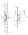
- FIG. 2 A better illustration of how the blow-down technique manipulates dislocations on semiconductor devices is shown in Figure 2 .
- a pre-existing dislocation or dislocation loop, generally designated by 20, below a wafer surface 22 is subjected to a laser beam 24 having a scan direction indicated by arrows 26.
- the laser beam 24 locally heats the region below the wafer surface 22.
- the dislocation 20 grows or increases in size while in the hot spot of the laser beam 24 as shown.
- the dislocation 20 moves where the beam is incident.
- the dislocation motion is indicated by arrows 28.
- the blow-down phenomenon occurs by itself when the maximum velocity reached by the dislocation 20 is less than the scan speed of the laser beam 24 as illustrated in Figure 2 .
- the dislocation 20 grows to the micron scale, but stops growing once the laser beam 24 passes the dislocation 20 as illustrated in Figures 3A and 3B.
- Figure 3A illustrates the dislocation 20 before the laser beam 24 passes through it while
- Figure 3B illustrates the dislocation 20 after the laser beam 24 passes through it.
- the blow-down effect is described using an LSA configuration, the blow-down effect may also occur using a flash annealing configuration.
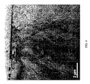
- Figure 4 illustrates a portion of a cross-sectional side view of wafer 10 in a magnified form.
- This exemplary figure shows the blow-down phenomena obtained by direct transmission electron microscopy (TEM) observations. Of course, other tools and methods of viewing the blow-down phenomena can be used as desired.
- This exemplary figure shows dislocations 20 blown down and away from the active region 14 by a 1250-Centigrade (C) laser scan.
- C 1250-Centigrade
- FIG. 5A-5B illustrates a second mode of operation in accordance with one exemplary embodiment.
- the second mode of operation is referred to herein as "surfing".
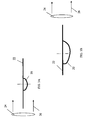
- surfing occurs when the temperature of the local hot spot of the laser beam 24 is placed high enough and the combination of laser stress and pre-existing layer strains is large enough to allow the dislocation 20 to grow with a speed that matches the speed of the laser beam 24.
- surfing occurs when the maximum value reached by the dislocation velocity equals or exceeds the scan speed of the laser beam.
- the laser beam 24 is controlled such that one end of the dislocation 20 keeps up with the moving hot spot of the laser beam 24, resulting in dislocation growth over the length of the laser scan.
- Figure 5A illustrates the dislocation before the hot spot of the laser beam passes through the dislocation while Figure 5B illustrates the dislocation after the hot spot of the laser beam passes the dislocation.
- one end of the dislocation 20 moves with and in the scan direction 26 of the laser beam 24. Surfing occurs only in an LSA configuration in accordance with one embodiment.
- surfing can be used to generate desired dislocation patterns or relax specific regions of a strained-engineering pattern by moving dislocations from a dislocation source into other areas.
- the laser beam can be used to draw out dislocations from any point on a layer along various paths as desired in an "etch-a-sketch" fashion.
- the temperature and dwell time (laser spot thickness/LSA scan speed) of the laser beam play a role in manipulating dislocations of various sizes in semiconductor technology. Dislocations become more active at higher temperatures and depending on the desired mode of operation the scan speed of the laser beam will determine whether dislocations will grow over the length of the scan.
- surfing-type growth generally occurs when the temperature of the laser beam is approximately above 1250 C and the scan speed is greater than about 1 millisecond (ms). At significantly lower temperatures or lower dwell times, surfing should not occur.
- the temperature and scan speed can be adjusted to avoid dragging dislocations from one part of the wafer to another.
- different wafer materials may affect the temperatures and dwell times needed to move dislocations from semiconductor technology or into the same depending on the application.
- the direction of the laser scan can also play a role in separately manipulating dislocations of various kinds in semiconductor technology in accordance with one exemplary embodiment. Dislocations move only on specific glide planes. Thus, dislocations on glide planes oriented perpendicular to the scan direction of the laser beam will not exhibit the surfing phenomena.
- the laser beam can be controlled so that only dislocations on glide planes oriented in one direction can be manipulated to obtain a desired dislocation pattern or a desired degree of asymmetric relaxation. However, all dislocations will exhibit the blow-up phenomena in some degree when the laser passes the dislocations.
- Dislocations on the wafer 10 can also be manipulated by adding a strained layer to the wafer 10 in accordance with one exemplary embodiment. Since dislocations move in response to strain (thermal-mismatch), adding additional strain to existing dislocations on the wafer 10 will enable the dislocations to move more quickly. For example, surfing may occur when adding a 50nm, 1% strained layer on a wafer subjected to a 1498 K laser scan.
- strain-inducing materials can also be used to manipulate dislocations since dislocations respond differently with different strain-inducing materials. In other words, dislocations move better with some materials and not with others. For example, surfing may not occur on dislocations in the 1498K scan with the strained layer as described above when the mobility of the dislocations is reduced by, for example, a factor of three.
- the methods described herein can be used to manipulate dislocations such that uniaxial layer relaxation or strain generation is provided.
- Figure 6 illustrates how to provide uniaxial layer relaxation or strain generation.
- the wafer 10 is fabricated to include an implanted region 50 and a non-implanted region 52.
- a raster scan generator raster scans from the implanted region containing dislocations into the non-implanted region, filling the latter with oriented dislocations.
- the implanted region is subjected to the laser beam 16 such that strain in the non-implanted region 52 is relaxed in one direction, thereby leaving strain only in one direction.
- Such a configuration can be useful for various applications.
- the surfing technique can be used to also remove threading dislocations from a relaxed strained layer as illustrated in Figure 7 .
- any threading dislocations i.e. ones that extend to the surface
- varying the temperature, the sweep speed, the absorption profile, and the spot-size of the laser beam 24 effectively varies the dislocation evolution.
- Various modeling techniques can be used to predict the phenomena described above and can be validated through direct experimental observations.
Landscapes
- Recrystallisation Techniques (AREA)
- Physics & Mathematics (AREA)
- Electromagnetism (AREA)
- Optics & Photonics (AREA)
- Chemical & Material Sciences (AREA)
- Crystallography & Structural Chemistry (AREA)
- Insulated Gate Type Field-Effect Transistor (AREA)
- Crystals, And After-Treatments Of Crystals (AREA)
Abstract
Description
- This invention relates to a system and method for manipulating dislocations in semiconductor devices using a scanned laser.
- Currently, 65 nanometer (nm) technology and beyond makes extensive use of strain engineering to optimize device performance. The appearance and uncontrolled behavior of dislocations in this context is a frequent source of problems, since these defects provide electrical leakage paths and also lead to undesired local strain variations. At the same time, the deliberate relaxation of strained layers by dislocation motion is a common technique of preparing substrates on which strained layers can be grown.
- An economic determinant of integrated circuit process technology is the yield, that is, the percentage of the total number of chips processed that are good. The yield of complex integrated circuits is typically a few percent. One major factor that affects this yield is the presence of crystal defects in silicon, or in other semiconductor wafers on which integrated circuits are built. Some of these crystal defects can be classified as dislocations, which can be introduced in high temperature processing when large strains are present.
-
US2002/090772 describes a method for generating a patterned strained region in a semi conductor wafer in which an amorphous silicon layer is deposited on a crystalline SiGe layer. Upon localized laser crystallization, the silicon is strained, due to the lattice mismatch. -
US2004/191975 describes the introduction of dislocations through implantation in a MOSFET substrate. - An exemplary embodiment of a method for generating patterned strained regions in a semiconductor device includes directing a light-emitting beam locally onto a surface portion of a semiconductor body; and manipulating a plurality of dislocations located proximate to the surface portion of the semiconductor body utilizing the light-emitting beam, the light-emitting beam being characterized as having a scan speed, so as to produce the patterned strained regions.
- The plurality of dislocations is preferably manipulated utilizing the light-emitting beam to generate specific dislocation patterns on the semiconductor body.
- An exemplary embodiment of a method for generating patterned strained regions in a semiconductor device includes directing a laser beam locally onto a surface portion of a semiconductor body; operating the laser beam in a first mode of operation or a second mode of operation, the laser beam having a scan speed; and manipulating a plurality of dislocations located proximate to the surface portion of the semiconductor body utilizing the laser beam so as to produce the patterned strained regions, the plurality of dislocations being manipulated during the first mode of operation and the second mode of operation.
- An exemplary embodiment of a system for manipulating dislocations on semiconductor devices includes a semiconductor body having a plurality of dislocations; and a moveable laser configured to generate a laser beam locally on a surface portion of the semiconductor body, the moveable laser having a scan speed, the moveable laser manipulates the plurality of dislocations proximate to the surface portion of the semiconductor body by adjusting the temperature and the scan speed of the laser beam.
- The subject matter which is regarded as the invention is particularly pointed out and distinctly claimed in the claims at the conclusion of the specification. The foregoing and other objects, features, and advantages of the invention are apparent from the following detailed description taken in conjunction with the accompanying drawings in which:
-
-
FIGS. 1-3 are various schematic cross sectional views of an exemplary semiconductor device subjected to a blow-down technique for manipulating substrate dislocations, in accordance with one exemplary embodiment of the present invention; -
FIG. 4 illustrates an exemplary microphotograph of a portion of a cross-sectional side view of a wafer exhibiting the blow-down phenomena in accordance with one exemplary embodiment of the present invention; -
FIGs. 5A and 5B are cross sectional views of an exemplary semiconductor device subjected to a surfing technique for manipulating substrate dislocations, in accordance with another exemplary embodiment of the present invention; -
FIG. 6 is a cross-sectional view of an exemplary semiconductor device subjected to the surfing technique for manipulating substrate dislocations to allow the generation of uniaxial strained regions, in accordance with one exemplary embodiment of the present invention; and -
FIG. 7 is a cross-sectional view of an exemplary semiconductor device subjected to the surfing technique to remove threading dislocations from a relaxed strained layer, in accordance with one exemplary embodiment of the present invention. - The detailed description explains the preferred embodiments of the invention, together with advantages and features, by way of example with reference to the drawings.
- The present invention and the various features and advantageous details thereof are explained more fully with reference to the non-limiting embodiments that are illustrated in the accompanying drawings and detailed in the following description. It should be noted that the features illustrated in the drawings are not necessarily drawn to scale. Descriptions of well-known or conventional components and processing techniques are omitted so as to not unnecessarily obscure the present invention in detail. The examples used herein are intended merely to facilitate an understanding of ways in which the invention may be practiced and to further enable those of skill in the art to practice the invention. Accordingly, the examples should not be construed as limiting the scope of the invention.
- Exemplary embodiments of the present invention provide systems and methods for manipulating dislocations in various semiconductor technologies by a light-emitting beam (e.g., laser beam). Dislocations subject to the beam will move where the beam is incident, allowing both temporal and spatial control of dislocation evolution. Such systems and methods provide modes of operation that illustrate two phenomena referred to herein as the blow-down and surfing phenomena. These phenomena can be utilized to perform various dislocation manipulations.
- The inventors herein have recognized that the systems and methods described herein eliminate dislocations present in silicon on insulator (SOI) technology devices. The systems and methods described herein further control dislocation growth during high-temperature laser annealing (LSA) and enable localized (patterned) relaxation of layer strain. The systems and methods described herein further enable the generation of uniaxially strained regions and enable the elimination of threading dislocations in a relaxed strained layer. Such systems and methods further enable the generation of specific dislocation patterns and their associated strain fields for use as templates for the spatially controlled grow of epitaxial islands and nanostructures.
- For a better understanding of the invention and its operation, turning now to the drawings,
Figure 1 illustrates a portion of a semiconductor body or wafer, designated generally by 10. In accordance with one exemplary embodiment, the wafer is made up of silicon. Of course, other suitable materials can be used to form the wafer such as germanium, gallium phosphate, gallium arsenide or the like. Thewafer 10 sits on an insulating layer, for example a buried oxide surface layer, which is indicated as lying below thedashed line 12. Thesemiconductor body 10 is fabricated to includeactive regions 14 where current flows and where semiconductor devices, such as transistors integrated circuits or the like, are to be formed. The wafer configuration can be varied to achieve various goals and should not be limited to the configurations shown herein. In other words, the configurations described herein are intended to illustrate the methods for manipulating dislocations on semiconductor technology and semiconductor substrates, thereby should not limit the scope of the exemplary embodiments of the present invention. - In accordance with one exemplary embodiment, a moving light-emitting beam, which is indicated by
arrow 16, directly scans over a surface portion of thewafer 10, and particularly over theactive regions 14 configured on thewafer 10. More specifically, the light-emittingbeam 16 heats thewafer 10 locally allowing dislocations present on thewafer 10 and most importantly on theactive regions 14 to move by increasing their mobility. Dislocations move due to pre-existing strains (e.g., SiGe on Si wafers) and because the beam producing source (e.g., laser) itself generates a large stress field moving along with the beam. As the dislocations are driven into the buried-oxide layer and the shallow-trench oxide, this effectively eliminates undesirable electrical leakage paths from forming. - The light-emitting beam can be generated through any source-type, such as a laser, configured to vary the temperature, the sweep speed, the absorption profile, and the spot-size of the beam. However, other beams from other sources may be used such as, for example, a lamp. For simplistic purposes, the methods herein will be described in the context of using a laser beam from a scanned laser device. Such a device is used in a scanned laser-annealing (LSA) configuration to move the dislocations as described herein. However, other configurations can be used in other exemplary embodiments of the present invention and should not be limited to the examples set forth herein.
- In accordance with one exemplary embodiment, the
laser beam 16 is controlled such that two distinct modes of operation for manipulating dislocations can be implemented. The first mode of operation is referred to herein as a "blow-down". In this mode of operation, stress from thelaser beam 16 drives dislocations into the substrate or into absorbing sinks such as buried oxide (BOX)layers 18 or into shallow trench isolation (STI) structures 19 as shown inFigure 1 . This mode of operation enables the elimination of already present dislocations in thewafer 10. - A better illustration of how the blow-down technique manipulates dislocations on semiconductor devices is shown in
Figure 2 . A pre-existing dislocation or dislocation loop, generally designated by 20, below awafer surface 22 is subjected to alaser beam 24 having a scan direction indicated byarrows 26. Thelaser beam 24 locally heats the region below thewafer surface 22. As a result, thedislocation 20 grows or increases in size while in the hot spot of thelaser beam 24 as shown. Thedislocation 20 moves where the beam is incident. The dislocation motion is indicated byarrows 28. The blow-down phenomenon occurs by itself when the maximum velocity reached by thedislocation 20 is less than the scan speed of thelaser beam 24 as illustrated inFigure 2 . Thedislocation 20 grows to the micron scale, but stops growing once thelaser beam 24 passes thedislocation 20 as illustrated inFigures 3A and 3B. Figure 3A illustrates thedislocation 20 before thelaser beam 24 passes through it whileFigure 3B illustrates thedislocation 20 after thelaser beam 24 passes through it. Although the blow-down effect is described using an LSA configuration, the blow-down effect may also occur using a flash annealing configuration. -
Figure 4 illustrates a portion of a cross-sectional side view ofwafer 10 in a magnified form. This exemplary figure shows the blow-down phenomena obtained by direct transmission electron microscopy (TEM) observations. Of course, other tools and methods of viewing the blow-down phenomena can be used as desired. This exemplary figure showsdislocations 20 blown down and away from theactive region 14 by a 1250-Centigrade (C) laser scan. -
Figure 5A-5B illustrates a second mode of operation in accordance with one exemplary embodiment. The second mode of operation is referred to herein as "surfing". Using the previous example to describe this mode of operation, surfing occurs when the temperature of the local hot spot of thelaser beam 24 is placed high enough and the combination of laser stress and pre-existing layer strains is large enough to allow thedislocation 20 to grow with a speed that matches the speed of thelaser beam 24. In other words, surfing occurs when the maximum value reached by the dislocation velocity equals or exceeds the scan speed of the laser beam. In this mode of operation, thelaser beam 24 is controlled such that one end of thedislocation 20 keeps up with the moving hot spot of thelaser beam 24, resulting in dislocation growth over the length of the laser scan.Figure 5A illustrates the dislocation before the hot spot of the laser beam passes through the dislocation whileFigure 5B illustrates the dislocation after the hot spot of the laser beam passes the dislocation. As shown, one end of thedislocation 20 moves with and in thescan direction 26 of thelaser beam 24. Surfing occurs only in an LSA configuration in accordance with one embodiment. - In accordance with one exemplary embodiment, surfing can be used to generate desired dislocation patterns or relax specific regions of a strained-engineering pattern by moving dislocations from a dislocation source into other areas. In other words, the laser beam can be used to draw out dislocations from any point on a layer along various paths as desired in an "etch-a-sketch" fashion.
- In accordance with one exemplary embodiment, the temperature and dwell time (laser spot thickness/LSA scan speed) of the laser beam play a role in manipulating dislocations of various sizes in semiconductor technology. Dislocations become more active at higher temperatures and depending on the desired mode of operation the scan speed of the laser beam will determine whether dislocations will grow over the length of the scan. In accordance with one exemplary embodiment, surfing-type growth generally occurs when the temperature of the laser beam is approximately above 1250 C and the scan speed is greater than about 1 millisecond (ms). At significantly lower temperatures or lower dwell times, surfing should not occur. For example, surfing does not occur on a 40 nano-micron (nm) dislocation loop when scanning a laser beam with a 1498 Kelvin (K) scan, while surfing occurs with a 1624 K scan. Thus, the temperature and scan speed can be adjusted to avoid dragging dislocations from one part of the wafer to another. It should be understood that different wafer materials may affect the temperatures and dwell times needed to move dislocations from semiconductor technology or into the same depending on the application. The direction of the laser scan can also play a role in separately manipulating dislocations of various kinds in semiconductor technology in accordance with one exemplary embodiment. Dislocations move only on specific glide planes. Thus, dislocations on glide planes oriented perpendicular to the scan direction of the laser beam will not exhibit the surfing phenomena. Only dislocations on glide planes oriented along the scan direction are subject to the surfing phenomenon. Thus, the laser beam can be controlled so that only dislocations on glide planes oriented in one direction can be manipulated to obtain a desired dislocation pattern or a desired degree of asymmetric relaxation. However, all dislocations will exhibit the blow-up phenomena in some degree when the laser passes the dislocations.
- Dislocations on the
wafer 10 can also be manipulated by adding a strained layer to thewafer 10 in accordance with one exemplary embodiment. Since dislocations move in response to strain (thermal-mismatch), adding additional strain to existing dislocations on thewafer 10 will enable the dislocations to move more quickly. For example, surfing may occur when adding a 50nm, 1% strained layer on a wafer subjected to a 1498 K laser scan. - Using different strain-inducing materials can also be used to manipulate dislocations since dislocations respond differently with different strain-inducing materials. In other words, dislocations move better with some materials and not with others. For example, surfing may not occur on dislocations in the 1498K scan with the strained layer as described above when the mobility of the dislocations is reduced by, for example, a factor of three.
- In accordance with one exemplary embodiment of the present invention, the methods described herein can be used to manipulate dislocations such that uniaxial layer relaxation or strain generation is provided.
Figure 6 illustrates how to provide uniaxial layer relaxation or strain generation. In this exemplary figure, thewafer 10 is fabricated to include an implantedregion 50 and anon-implanted region 52. In accordance with one embodiment, a raster scan generator raster scans from the implanted region containing dislocations into the non-implanted region, filling the latter with oriented dislocations. In operation, the implanted region is subjected to thelaser beam 16 such that strain in thenon-implanted region 52 is relaxed in one direction, thereby leaving strain only in one direction. Such a configuration can be useful for various applications. - In accordance with one exemplary embodiment, the surfing technique can be used to also remove threading dislocations from a relaxed strained layer as illustrated in
Figure 7 . Here, any threading dislocations (i.e. ones that extend to the surface) can be swept out of the region of interest by rastering a laser beam operating in the surfing mode. This removes potential sources of leakage paths from the region of the wafer on which microelectronic devices are to be constructed. - In the above embodiment, varying the temperature, the sweep speed, the absorption profile, and the spot-size of the
laser beam 24 effectively varies the dislocation evolution. Various modeling techniques can be used to predict the phenomena described above and can be validated through direct experimental observations.
Claims (15)
- A method for generating patterned strained regions in a semiconductor device, comprising:directing a light-emitting beam (16) locally onto a surface portion of the semiconductor body (10); andmanipulating a plurality of dislocations (20) located proximate to the surface portion of the semiconductor body utilizing the light-emitting beam, the light-emitting beam being characterized as having a scan speed, so as to produce the patterned strained regions.
- The method as in claim 1, wherein manipulating the plurality of dislocations comprises directly heating the plurality of dislocations with the light-emitting beam such that the plurality of dislocations are driven away from the surface portion of the semiconductor body enabling the elimination of the plurality of dislocations on the semiconductor body.
- A method as claimed in claim 1 wherein the light beam comprises a laser beam (24) and the method comprises
operating the laser beam in a first mode of operation or a second mode of operation, the laser beam having a scan speed; and
manipulating a plurality of dislocations located proximate to the surface portion of the semiconductor body utilizing the laser beam so as to produce the patterned strained regions, the plurality of dislocations being manipulated during the first mode of operation and the second mode of operation. - The method as in claim 3, wherein the first mode of operation comprises directly heating the plurality of dislocation with the laser beam such that the plurality of dislocations are driven away from the surface portion of the semiconductor body enabling the elimination of the plurality of dislocations on the semiconductor body.
- The method as in claim 2 or claim 4, wherein directly heating the plurality of dislocations with the light-emitting beam enables the plurality of dislocations to be driven out from a dislocation source into another area of the semiconductor body.
- The method as in claim 2 or claim 4, wherein the light-emitting beam operably controls the growth of the plurality of dislocations during heating.
- The method as in claim 2 or claim 4, wherein the light-emitting beam drives the plurality of dislocations away from the surface portion of the semiconductor body when the plurality of dislocations move at a maximum velocity less than the scan speed of the light-emitting beam.
- The method as in claim 1, wherein manipulating the plurality of dislocations comprises scanning across the plurality of dislocations with the light-emitting beam such that the plurality of dislocations grow over the length of the scan of the light-emitting beam.
- The method as in claim 2, wherein the second mode of operation comprises scanning across the plurality of dislocations with the laser beam such that the plurality of dislocations grow over the length of the scan of the laser beam enabling the removal of threading dislocations from a relaxed layer on the semiconductor device.
- The method as in claim 8 or claim 9, wherein the plurality of dislocations grow over the length of the scan of the light-emitting beam when the plurality of dislocations move at a maximum velocity equal to or greater than the scan speed of the light-emitting beam.
- The method as in claim 8 or claim 9, wherein at least one end of each of the plurality of dislocations moves simultaneously with and in the scan direction of the light-emitting beam when the light-emitting beam scans across the plurality of dislocations.
- The method as in claim 8 or claim 9, wherein the plurality of dislocations grow over the length of the scan of the light-emitting beam when the scan speed of the light-emitting beam is approximately greater than 1250 degrees Centigrade and the scan speed of the light-emitting beam is greater than approximately 1 millisecond.
- The method as in claim 8, wherein scanning across the plurality of dislocations with the light-emitting beam such that the plurality of dislocations grow over the length of the scan of the light-emitting beam enables the removal of threading dislocations from a relaxed layer on the semiconductor device.
- The method as in claim 9, wherein the laser beam is configured to operably generate uniaxally strained regions in the semiconductor body.
- A system for manipulating dislocations on semiconductor devices, comprising:a semiconductor body (10) having a plurality of dislocations (20); anda moveable laser configured to generate a laser beam (24) locally on a surface portion of the semiconductor body, the moveable laser being characterized as having a scan speed, the moveable laser manipulates the plurality of dislocations on the surface portion of the semiconductor body by adjusting the temperature and the scan speed of the laser beam.
Applications Claiming Priority (2)
| Application Number | Priority Date | Filing Date | Title |
|---|---|---|---|
| US12/242,990 US8138066B2 (en) | 2008-10-01 | 2008-10-01 | Dislocation engineering using a scanned laser |
| PCT/EP2009/059552 WO2010037577A1 (en) | 2008-10-01 | 2009-07-24 | Dislocation engineering using a scanned laser |
Publications (2)
| Publication Number | Publication Date |
|---|---|
| EP2332168A1 EP2332168A1 (en) | 2011-06-15 |
| EP2332168B1 true EP2332168B1 (en) | 2011-11-16 |
Family
ID=41134607
Family Applications (1)
| Application Number | Title | Priority Date | Filing Date |
|---|---|---|---|
| EP09781028A Not-in-force EP2332168B1 (en) | 2008-10-01 | 2009-07-24 | Dislocation engineering using a scanned laser |
Country Status (7)
| Country | Link |
|---|---|
| US (5) | US8138066B2 (en) |
| EP (1) | EP2332168B1 (en) |
| JP (1) | JP5005115B2 (en) |
| KR (1) | KR101475992B1 (en) |
| AT (1) | ATE534139T1 (en) |
| TW (1) | TWI463755B (en) |
| WO (1) | WO2010037577A1 (en) |
Families Citing this family (5)
| Publication number | Priority date | Publication date | Assignee | Title |
|---|---|---|---|---|
| US8138066B2 (en) | 2008-10-01 | 2012-03-20 | International Business Machines Corporation | Dislocation engineering using a scanned laser |
| FR2974941B1 (en) * | 2011-05-06 | 2013-06-14 | Commissariat Energie Atomique | PROCESS FOR MAKING NANOCRYSTALS |
| FR2974940B1 (en) * | 2011-05-06 | 2015-11-13 | Commissariat Energie Atomique | PROCESS FOR PRODUCING SEMICONDUCTOR NANOCRYSTALS ORIENTED ACCORDING TO A PRE-DEFINED DIRECTION |
| CN103913687B (en) * | 2013-01-06 | 2016-12-28 | 上海华虹宏力半导体制造有限公司 | Groove MOS device Dislocations type analysis for current leakage method |
| CN114662346B (en) * | 2022-05-24 | 2022-08-09 | 山东大学 | A Simulation and Prediction Method of Dislocation Propagation Characteristics in Semiconductor Lasers |
Family Cites Families (39)
| Publication number | Priority date | Publication date | Assignee | Title |
|---|---|---|---|---|
| US4131487A (en) * | 1977-10-26 | 1978-12-26 | Western Electric Company, Inc. | Gettering semiconductor wafers with a high energy laser beam |
| DE2829983A1 (en) * | 1978-07-07 | 1980-01-24 | Siemens Ag | METHOD FOR SETTING SEMICONDUCTOR COMPONENTS AND INTEGRATED SEMICONDUCTOR CIRCUITS |
| US4257827A (en) * | 1979-11-13 | 1981-03-24 | International Business Machines Corporation | High efficiency gettering in silicon through localized superheated melt formation |
| JPS62172715A (en) * | 1986-01-27 | 1987-07-29 | Nippon Telegr & Teleph Corp <Ntt> | Manufacture of semiconductor epitaxial thin film |
| US4789788A (en) * | 1987-01-15 | 1988-12-06 | The Boeing Company | Optically pumped radiation source |
| JPH0449629A (en) * | 1990-06-18 | 1992-02-19 | Fujitsu Ltd | Compound semiconductor crystal and its manufacturing method |
| JPH0472735A (en) * | 1990-07-13 | 1992-03-06 | Mitsubishi Materials Corp | Process of gettering semiconductor wafer |
| JPH04107828A (en) * | 1990-08-28 | 1992-04-09 | Oki Electric Ind Co Ltd | Reducing method for dislocation in compound semiconductor layer |
| JPH04271114A (en) * | 1990-12-27 | 1992-09-28 | Nagoya Kogyo Univ | Defect reduction method of compound semiconductor |
| US5091767A (en) * | 1991-03-18 | 1992-02-25 | At&T Bell Laboratories | Article comprising a lattice-mismatched semiconductor heterostructure |
| CA2062134C (en) * | 1991-05-31 | 1997-03-25 | Ibm | Heteroepitaxial layers with low defect density and arbitrary network parameter |
| JPH0512307A (en) | 1991-07-03 | 1993-01-22 | Nec Corp | Production advance alarm display system |
| JP3376211B2 (en) * | 1996-05-29 | 2003-02-10 | 株式会社東芝 | Semiconductor device, method of manufacturing semiconductor substrate, and method of manufacturing semiconductor device |
| US5891769A (en) * | 1997-04-07 | 1999-04-06 | Motorola, Inc. | Method for forming a semiconductor device having a heteroepitaxial layer |
| DE60039875D1 (en) * | 1999-06-25 | 2008-09-25 | Massachusetts Inst Technology | CYCLIC THERMAL HEALING METHOD FOR REDUCING CRYSTAL TRANSLATION |
| US6514339B1 (en) * | 1999-10-29 | 2003-02-04 | Lg. Philips Co., Ltd. | Laser annealing apparatus |
| US7335260B2 (en) * | 1999-10-29 | 2008-02-26 | Lg.Philips Lcd Co., Ltd. | Laser annealing apparatus |
| US6503773B2 (en) * | 2000-01-20 | 2003-01-07 | Amberwave Systems Corporation | Low threading dislocation density relaxed mismatched epilayers without high temperature growth |
| JP2002093735A (en) * | 2000-09-13 | 2002-03-29 | Sony Corp | Method for manufacturing semiconductor device |
| JP4511092B2 (en) * | 2000-12-11 | 2010-07-28 | セイコーエプソン株式会社 | Manufacturing method of semiconductor device |
| US6613652B2 (en) * | 2001-03-14 | 2003-09-02 | Chartered Semiconductor Manufacturing Ltd. | Method for fabricating SOI devices with option of incorporating air-gap feature for better insulation and performance |
| AU2002348835A1 (en) * | 2001-11-30 | 2003-06-10 | Koninklijke Philips Electronics N.V. | Method of manufacturing a semiconductor device |
| JP4279498B2 (en) * | 2002-02-28 | 2009-06-17 | 株式会社 液晶先端技術開発センター | Semiconductor thin film forming method, semiconductor thin film forming apparatus, and crystallization method |
| JP2004049629A (en) | 2002-07-22 | 2004-02-19 | Daikoku Denki Co Ltd | Pachinko machine management device |
| US6773513B2 (en) * | 2002-08-13 | 2004-08-10 | Ut-Battelle Llc | Method for residual stress relief and retained austenite destabilization |
| US20040038438A1 (en) * | 2002-08-23 | 2004-02-26 | Toppoly Optoelectronics Corp. | Method for reducing surface roughness of polysilicon films for liquid crystal displays |
| JP4022576B2 (en) | 2002-09-19 | 2007-12-19 | 港屋株式会社 | Fluorescent yarn, method for producing the same, and yarn product using the same |
| US6800887B1 (en) * | 2003-03-31 | 2004-10-05 | Intel Corporation | Nitrogen controlled growth of dislocation loop in stress enhanced transistor |
| US6972247B2 (en) * | 2003-12-05 | 2005-12-06 | International Business Machines Corporation | Method of fabricating strained Si SOI wafers |
| WO2005112129A1 (en) * | 2004-05-13 | 2005-11-24 | Fujitsu Limited | Semiconductor device and process for fabricating same, and process for producing semiconductor substrate |
| US7202145B2 (en) * | 2004-06-03 | 2007-04-10 | Taiwan Semiconductor Manufacturing Company | Strained Si formed by anneal |
| US7273800B2 (en) * | 2004-11-01 | 2007-09-25 | International Business Machines Corporation | Hetero-integrated strained silicon n- and p-MOSFETs |
| US7232730B2 (en) * | 2005-04-29 | 2007-06-19 | Taiwan Semiconductor Manufacturing Company, Ltd. | Method of forming a locally strained transistor |
| US7186626B2 (en) * | 2005-07-22 | 2007-03-06 | The Regents Of The University Of California | Method for controlling dislocation positions in silicon germanium buffer layers |
| US20080045041A1 (en) * | 2006-08-17 | 2008-02-21 | Toshiba America Electronic Components, Inc. | Liquid Immersion Laser Spike Anneal |
| JP2008198656A (en) * | 2007-02-08 | 2008-08-28 | Shin Etsu Chem Co Ltd | Manufacturing method of semiconductor substrate |
| US7732353B2 (en) * | 2007-04-18 | 2010-06-08 | Ultratech, Inc. | Methods of forming a denuded zone in a semiconductor wafer using rapid laser annealing |
| US7863710B2 (en) * | 2008-02-15 | 2011-01-04 | Intel Corporation | Dislocation removal from a group III-V film grown on a semiconductor substrate |
| US8138066B2 (en) * | 2008-10-01 | 2012-03-20 | International Business Machines Corporation | Dislocation engineering using a scanned laser |
-
2008
- 2008-10-01 US US12/242,990 patent/US8138066B2/en not_active Expired - Fee Related
-
2009
- 2009-07-24 JP JP2011529490A patent/JP5005115B2/en not_active Expired - Fee Related
- 2009-07-24 AT AT09781028T patent/ATE534139T1/en active
- 2009-07-24 KR KR1020117007783A patent/KR101475992B1/en not_active Expired - Fee Related
- 2009-07-24 WO PCT/EP2009/059552 patent/WO2010037577A1/en not_active Ceased
- 2009-07-24 EP EP09781028A patent/EP2332168B1/en not_active Not-in-force
- 2009-09-28 TW TW098132667A patent/TWI463755B/en not_active IP Right Cessation
-
2012
- 2012-02-14 US US13/372,713 patent/US20120138823A1/en not_active Abandoned
- 2012-08-02 US US13/565,018 patent/US20120294322A1/en not_active Abandoned
-
2014
- 2014-02-07 US US14/174,868 patent/US8865571B2/en not_active Expired - Fee Related
- 2014-02-07 US US14/174,869 patent/US8865572B2/en not_active Expired - Fee Related
Also Published As
| Publication number | Publication date |
|---|---|
| US20140154873A1 (en) | 2014-06-05 |
| JP2012504857A (en) | 2012-02-23 |
| JP5005115B2 (en) | 2012-08-22 |
| US8865571B2 (en) | 2014-10-21 |
| US8138066B2 (en) | 2012-03-20 |
| TWI463755B (en) | 2014-12-01 |
| US20120138823A1 (en) | 2012-06-07 |
| WO2010037577A1 (en) | 2010-04-08 |
| ATE534139T1 (en) | 2011-12-15 |
| TW201015807A (en) | 2010-04-16 |
| KR20110081965A (en) | 2011-07-15 |
| US20100081259A1 (en) | 2010-04-01 |
| US8865572B2 (en) | 2014-10-21 |
| EP2332168A1 (en) | 2011-06-15 |
| US20140154872A1 (en) | 2014-06-05 |
| US20120294322A1 (en) | 2012-11-22 |
| KR101475992B1 (en) | 2014-12-30 |
Similar Documents
| Publication | Publication Date | Title |
|---|---|---|
| US7524740B1 (en) | Localized strain relaxation for strained Si directly on insulator | |
| US8865572B2 (en) | Dislocation engineering using a scanned laser | |
| US9899217B2 (en) | Method for producing a strained semiconductor on insulator substrate | |
| US20020185686A1 (en) | Relaxed SiGe layers on Si or silicon-on-insulator substrates by ion implantation and thermal annealing | |
| CN101228616B (en) | Method for controlling dislocation position in silicon germanium buffer layer and article produced thereby | |
| US9799513B2 (en) | Localized elastic strain relaxed buffer | |
| CN107665919B (en) | Semiconductor element and method for manufacturing semiconductor element | |
| KR20100067061A (en) | Systems and processes for forming three-dimensional circuits | |
| US7944023B2 (en) | Strained Si formed by anneal | |
| Prucnal et al. | III-V/Si on silicon-on-insulator platform for hybrid nanoelectronics | |
| US20070163489A1 (en) | Method of forming a layer having a single crystalline structure | |
| US12374545B2 (en) | Process for working a wafer of 4H—SiC material to form a 3C—SiC layer in direct contact with the 4H—SiC material | |
| Chen et al. | Ultrathin low temperature Si0. 75Ge0. 25/Si buffer layer for the growth of high quality Ge epilayer on Si (100) by RPCVD | |
| Vellianitis et al. | High crystalline quality Ge grown by MOCVD inside narrow shallow trench isolation defined on Si (001) substrates | |
| CN108400089A (en) | A kind of laser anneal method | |
| Wutzler et al. | III–V nanocrystal formation in ion-implanted Ge and Si via liquid phase epitaxy during short-time flash lamp annealing | |
| US20060102888A1 (en) | Semiconductor substrate and method of fabricating the same | |
| CN107785461B (en) | A kind of laser assisted direct band gap Ge and preparation method thereof on crystallization Ge/Si void substrate again | |
| Tabata et al. | Solid phase recrystallization and dopant activation in arsenic ion-implanted silicon-on-insulator by UV laser annealing | |
| JP2006032575A (en) | Epitaxial growth substrate, method for producing the same, and multilayer structure | |
| JP5156950B2 (en) | Method for producing strain-relieving germanium film and multilayer structure | |
| Baidakova et al. | Growth of light-emitting SiGe heterostructures on strained silicon-on-insulator substrates with a thin oxide layer | |
| Hartmann | Epitaxy of Ge layers on blanket and patterned Si (001) for nanoelectronics and optoelectronics | |
| GB2112205A (en) | A thermal processing system for semiconductors and other materials using two or more electron beams | |
| Weng et al. | Dislocation formation during laser processing of silicon solar cell materials |
Legal Events
| Date | Code | Title | Description |
|---|---|---|---|
| PUAI | Public reference made under article 153(3) epc to a published international application that has entered the european phase |
Free format text: ORIGINAL CODE: 0009012 |
|
| 17P | Request for examination filed |
Effective date: 20101105 |
|
| AK | Designated contracting states |
Kind code of ref document: A1 Designated state(s): AT BE BG CH CY CZ DE DK EE ES FI FR GB GR HR HU IE IS IT LI LT LU LV MC MK MT NL NO PL PT RO SE SI SK SM TR |
|
| AX | Request for extension of the european patent |
Extension state: AL BA RS |
|
| GRAP | Despatch of communication of intention to grant a patent |
Free format text: ORIGINAL CODE: EPIDOSNIGR1 |
|
| GRAS | Grant fee paid |
Free format text: ORIGINAL CODE: EPIDOSNIGR3 |
|
| GRAA | (expected) grant |
Free format text: ORIGINAL CODE: 0009210 |
|
| AK | Designated contracting states |
Kind code of ref document: B1 Designated state(s): AT BE BG CH CY CZ DE DK EE ES FI FR GB GR HR HU IE IS IT LI LT LU LV MC MK MT NL NO PL PT RO SE SI SK SM TR |
|
| DAX | Request for extension of the european patent (deleted) | ||
| REG | Reference to a national code |
Ref country code: GB Ref legal event code: FG4D |
|
| REG | Reference to a national code |
Ref country code: CH Ref legal event code: NV Representative=s name: IBM RESEARCH GMBH ZURICH RESEARCH LABORATORY INTEL Ref country code: CH Ref legal event code: EP |
|
| REG | Reference to a national code |
Ref country code: IE Ref legal event code: FG4D |
|
| REG | Reference to a national code |
Ref country code: GB Ref legal event code: 746 Effective date: 20120103 |
|
| REG | Reference to a national code |
Ref country code: DE Ref legal event code: R096 Ref document number: 602009003778 Country of ref document: DE Effective date: 20120202 |
|
| REG | Reference to a national code |
Ref country code: NL Ref legal event code: VDEP Effective date: 20111116 |
|
| REG | Reference to a national code |
Ref country code: DE Ref legal event code: R084 Ref document number: 602009003778 Country of ref document: DE Effective date: 20120110 |
|
| LTIE | Lt: invalidation of european patent or patent extension |
Effective date: 20111116 |
|
| PG25 | Lapsed in a contracting state [announced via postgrant information from national office to epo] |
Ref country code: LT Free format text: LAPSE BECAUSE OF FAILURE TO SUBMIT A TRANSLATION OF THE DESCRIPTION OR TO PAY THE FEE WITHIN THE PRESCRIBED TIME-LIMIT Effective date: 20111116 Ref country code: IS Free format text: LAPSE BECAUSE OF FAILURE TO SUBMIT A TRANSLATION OF THE DESCRIPTION OR TO PAY THE FEE WITHIN THE PRESCRIBED TIME-LIMIT Effective date: 20120316 Ref country code: NO Free format text: LAPSE BECAUSE OF FAILURE TO SUBMIT A TRANSLATION OF THE DESCRIPTION OR TO PAY THE FEE WITHIN THE PRESCRIBED TIME-LIMIT Effective date: 20120216 |
|
| PG25 | Lapsed in a contracting state [announced via postgrant information from national office to epo] |
Ref country code: SE Free format text: LAPSE BECAUSE OF FAILURE TO SUBMIT A TRANSLATION OF THE DESCRIPTION OR TO PAY THE FEE WITHIN THE PRESCRIBED TIME-LIMIT Effective date: 20111116 Ref country code: PT Free format text: LAPSE BECAUSE OF FAILURE TO SUBMIT A TRANSLATION OF THE DESCRIPTION OR TO PAY THE FEE WITHIN THE PRESCRIBED TIME-LIMIT Effective date: 20120316 Ref country code: SI Free format text: LAPSE BECAUSE OF FAILURE TO SUBMIT A TRANSLATION OF THE DESCRIPTION OR TO PAY THE FEE WITHIN THE PRESCRIBED TIME-LIMIT Effective date: 20111116 Ref country code: HR Free format text: LAPSE BECAUSE OF FAILURE TO SUBMIT A TRANSLATION OF THE DESCRIPTION OR TO PAY THE FEE WITHIN THE PRESCRIBED TIME-LIMIT Effective date: 20111116 Ref country code: BE Free format text: LAPSE BECAUSE OF FAILURE TO SUBMIT A TRANSLATION OF THE DESCRIPTION OR TO PAY THE FEE WITHIN THE PRESCRIBED TIME-LIMIT Effective date: 20111116 Ref country code: LV Free format text: LAPSE BECAUSE OF FAILURE TO SUBMIT A TRANSLATION OF THE DESCRIPTION OR TO PAY THE FEE WITHIN THE PRESCRIBED TIME-LIMIT Effective date: 20111116 Ref country code: PL Free format text: LAPSE BECAUSE OF FAILURE TO SUBMIT A TRANSLATION OF THE DESCRIPTION OR TO PAY THE FEE WITHIN THE PRESCRIBED TIME-LIMIT Effective date: 20111116 Ref country code: NL Free format text: LAPSE BECAUSE OF FAILURE TO SUBMIT A TRANSLATION OF THE DESCRIPTION OR TO PAY THE FEE WITHIN THE PRESCRIBED TIME-LIMIT Effective date: 20111116 Ref country code: GR Free format text: LAPSE BECAUSE OF FAILURE TO SUBMIT A TRANSLATION OF THE DESCRIPTION OR TO PAY THE FEE WITHIN THE PRESCRIBED TIME-LIMIT Effective date: 20120217 |
|
| PG25 | Lapsed in a contracting state [announced via postgrant information from national office to epo] |
Ref country code: CY Free format text: LAPSE BECAUSE OF FAILURE TO SUBMIT A TRANSLATION OF THE DESCRIPTION OR TO PAY THE FEE WITHIN THE PRESCRIBED TIME-LIMIT Effective date: 20111116 |
|
| PG25 | Lapsed in a contracting state [announced via postgrant information from national office to epo] |
Ref country code: BG Free format text: LAPSE BECAUSE OF FAILURE TO SUBMIT A TRANSLATION OF THE DESCRIPTION OR TO PAY THE FEE WITHIN THE PRESCRIBED TIME-LIMIT Effective date: 20120216 Ref country code: SK Free format text: LAPSE BECAUSE OF FAILURE TO SUBMIT A TRANSLATION OF THE DESCRIPTION OR TO PAY THE FEE WITHIN THE PRESCRIBED TIME-LIMIT Effective date: 20111116 Ref country code: DK Free format text: LAPSE BECAUSE OF FAILURE TO SUBMIT A TRANSLATION OF THE DESCRIPTION OR TO PAY THE FEE WITHIN THE PRESCRIBED TIME-LIMIT Effective date: 20111116 Ref country code: EE Free format text: LAPSE BECAUSE OF FAILURE TO SUBMIT A TRANSLATION OF THE DESCRIPTION OR TO PAY THE FEE WITHIN THE PRESCRIBED TIME-LIMIT Effective date: 20111116 Ref country code: CZ Free format text: LAPSE BECAUSE OF FAILURE TO SUBMIT A TRANSLATION OF THE DESCRIPTION OR TO PAY THE FEE WITHIN THE PRESCRIBED TIME-LIMIT Effective date: 20111116 |
|
| PG25 | Lapsed in a contracting state [announced via postgrant information from national office to epo] |
Ref country code: IT Free format text: LAPSE BECAUSE OF FAILURE TO SUBMIT A TRANSLATION OF THE DESCRIPTION OR TO PAY THE FEE WITHIN THE PRESCRIBED TIME-LIMIT Effective date: 20111116 Ref country code: RO Free format text: LAPSE BECAUSE OF FAILURE TO SUBMIT A TRANSLATION OF THE DESCRIPTION OR TO PAY THE FEE WITHIN THE PRESCRIBED TIME-LIMIT Effective date: 20111116 |
|
| REG | Reference to a national code |
Ref country code: AT Ref legal event code: MK05 Ref document number: 534139 Country of ref document: AT Kind code of ref document: T Effective date: 20111116 |
|
| PLBE | No opposition filed within time limit |
Free format text: ORIGINAL CODE: 0009261 |
|
| STAA | Information on the status of an ep patent application or granted ep patent |
Free format text: STATUS: NO OPPOSITION FILED WITHIN TIME LIMIT |
|
| 26N | No opposition filed |
Effective date: 20120817 |
|
| REG | Reference to a national code |
Ref country code: DE Ref legal event code: R097 Ref document number: 602009003778 Country of ref document: DE Effective date: 20120817 |
|
| PGFP | Annual fee paid to national office [announced via postgrant information from national office to epo] |
Ref country code: FR Payment date: 20120731 Year of fee payment: 4 |
|
| PG25 | Lapsed in a contracting state [announced via postgrant information from national office to epo] |
Ref country code: AT Free format text: LAPSE BECAUSE OF FAILURE TO SUBMIT A TRANSLATION OF THE DESCRIPTION OR TO PAY THE FEE WITHIN THE PRESCRIBED TIME-LIMIT Effective date: 20111116 |
|
| PG25 | Lapsed in a contracting state [announced via postgrant information from national office to epo] |
Ref country code: MK Free format text: LAPSE BECAUSE OF FAILURE TO SUBMIT A TRANSLATION OF THE DESCRIPTION OR TO PAY THE FEE WITHIN THE PRESCRIBED TIME-LIMIT Effective date: 20111116 Ref country code: MC Free format text: LAPSE BECAUSE OF NON-PAYMENT OF DUE FEES Effective date: 20120731 |
|
| PG25 | Lapsed in a contracting state [announced via postgrant information from national office to epo] |
Ref country code: ES Free format text: LAPSE BECAUSE OF FAILURE TO SUBMIT A TRANSLATION OF THE DESCRIPTION OR TO PAY THE FEE WITHIN THE PRESCRIBED TIME-LIMIT Effective date: 20120227 |
|
| REG | Reference to a national code |
Ref country code: IE Ref legal event code: MM4A |
|
| PG25 | Lapsed in a contracting state [announced via postgrant information from national office to epo] |
Ref country code: FI Free format text: LAPSE BECAUSE OF FAILURE TO SUBMIT A TRANSLATION OF THE DESCRIPTION OR TO PAY THE FEE WITHIN THE PRESCRIBED TIME-LIMIT Effective date: 20111116 |
|
| PG25 | Lapsed in a contracting state [announced via postgrant information from national office to epo] |
Ref country code: MT Free format text: LAPSE BECAUSE OF FAILURE TO SUBMIT A TRANSLATION OF THE DESCRIPTION OR TO PAY THE FEE WITHIN THE PRESCRIBED TIME-LIMIT Effective date: 20111116 Ref country code: IE Free format text: LAPSE BECAUSE OF NON-PAYMENT OF DUE FEES Effective date: 20120724 |
|
| REG | Reference to a national code |
Ref country code: CH Ref legal event code: PL |
|
| REG | Reference to a national code |
Ref country code: FR Ref legal event code: ST Effective date: 20140331 |
|
| PG25 | Lapsed in a contracting state [announced via postgrant information from national office to epo] |
Ref country code: CH Free format text: LAPSE BECAUSE OF NON-PAYMENT OF DUE FEES Effective date: 20130731 Ref country code: LI Free format text: LAPSE BECAUSE OF NON-PAYMENT OF DUE FEES Effective date: 20130731 Ref country code: TR Free format text: LAPSE BECAUSE OF FAILURE TO SUBMIT A TRANSLATION OF THE DESCRIPTION OR TO PAY THE FEE WITHIN THE PRESCRIBED TIME-LIMIT Effective date: 20111116 |
|
| PG25 | Lapsed in a contracting state [announced via postgrant information from national office to epo] |
Ref country code: LU Free format text: LAPSE BECAUSE OF NON-PAYMENT OF DUE FEES Effective date: 20120724 Ref country code: SM Free format text: LAPSE BECAUSE OF FAILURE TO SUBMIT A TRANSLATION OF THE DESCRIPTION OR TO PAY THE FEE WITHIN THE PRESCRIBED TIME-LIMIT Effective date: 20111116 Ref country code: FR Free format text: LAPSE BECAUSE OF NON-PAYMENT OF DUE FEES Effective date: 20130731 |
|
| PG25 | Lapsed in a contracting state [announced via postgrant information from national office to epo] |
Ref country code: HU Free format text: LAPSE BECAUSE OF FAILURE TO SUBMIT A TRANSLATION OF THE DESCRIPTION OR TO PAY THE FEE WITHIN THE PRESCRIBED TIME-LIMIT Effective date: 20090724 |
|
| PGFP | Annual fee paid to national office [announced via postgrant information from national office to epo] |
Ref country code: GB Payment date: 20150722 Year of fee payment: 7 |
|
| REG | Reference to a national code |
Ref country code: DE Ref legal event code: R082 Ref document number: 602009003778 Country of ref document: DE Representative=s name: RICHARDT PATENTANWAELTE PARTG MBB, DE Ref country code: DE Ref legal event code: R081 Ref document number: 602009003778 Country of ref document: DE Owner name: GLOBALFOUNDRIES INC., KY Free format text: FORMER OWNER: INTERNATIONAL BUSINESS MACHINES CORPORATION, ARMONK, N.Y., US |
|
| REG | Reference to a national code |
Ref country code: DE Ref legal event code: R082 Ref document number: 602009003778 Country of ref document: DE Representative=s name: RICHARDT PATENTANWAELTE PARTG MBB, DE Ref country code: DE Ref legal event code: R081 Ref document number: 602009003778 Country of ref document: DE Owner name: GLOBALFOUNDRIES INC., KY Free format text: FORMER OWNER: GLOBALFOUNDRIES US 2 LLC (N.D.GES.DES STAATES DELAWARE), HOPEWELL JUNCTION, N.Y., US |
|
| REG | Reference to a national code |
Ref country code: FR Ref legal event code: TP Owner name: GLOBALFOUNDRIES INC., GB Effective date: 20160829 |
|
| GBPC | Gb: european patent ceased through non-payment of renewal fee |
Effective date: 20160724 |
|
| PG25 | Lapsed in a contracting state [announced via postgrant information from national office to epo] |
Ref country code: GB Free format text: LAPSE BECAUSE OF NON-PAYMENT OF DUE FEES Effective date: 20160724 |
|
| PGFP | Annual fee paid to national office [announced via postgrant information from national office to epo] |
Ref country code: DE Payment date: 20180710 Year of fee payment: 10 |
|
| REG | Reference to a national code |
Ref country code: DE Ref legal event code: R119 Ref document number: 602009003778 Country of ref document: DE |
|
| PG25 | Lapsed in a contracting state [announced via postgrant information from national office to epo] |
Ref country code: DE Free format text: LAPSE BECAUSE OF NON-PAYMENT OF DUE FEES Effective date: 20200201 |