EP2328361A1 - Capacitive vibration sensor - Google Patents
Capacitive vibration sensor Download PDFInfo
- Publication number
- EP2328361A1 EP2328361A1 EP09809435A EP09809435A EP2328361A1 EP 2328361 A1 EP2328361 A1 EP 2328361A1 EP 09809435 A EP09809435 A EP 09809435A EP 09809435 A EP09809435 A EP 09809435A EP 2328361 A1 EP2328361 A1 EP 2328361A1
- Authority
- EP
- European Patent Office
- Prior art keywords
- electrode plate
- fixed electrode
- side wall
- reinforcement film
- film
- Prior art date
- Legal status (The legal status is an assumption and is not a legal conclusion. Google has not performed a legal analysis and makes no representation as to the accuracy of the status listed.)
- Granted
Links
Images








Classifications
-
- H—ELECTRICITY
- H04—ELECTRIC COMMUNICATION TECHNIQUE
- H04R—LOUDSPEAKERS, MICROPHONES, GRAMOPHONE PICK-UPS OR LIKE ACOUSTIC ELECTROMECHANICAL TRANSDUCERS; ELECTRIC HEARING AIDS; PUBLIC ADDRESS SYSTEMS
- H04R19/00—Electrostatic transducers
- H04R19/005—Electrostatic transducers using semiconductor materials
-
- B—PERFORMING OPERATIONS; TRANSPORTING
- B81—MICROSTRUCTURAL TECHNOLOGY
- B81B—MICROSTRUCTURAL DEVICES OR SYSTEMS, e.g. MICROMECHANICAL DEVICES
- B81B3/00—Devices comprising flexible or deformable elements, e.g. comprising elastic tongues or membranes
- B81B3/0064—Constitution or structural means for improving or controlling the physical properties of a device
- B81B3/0067—Mechanical properties
- B81B3/007—For controlling stiffness, e.g. ribs
-
- B—PERFORMING OPERATIONS; TRANSPORTING
- B81—MICROSTRUCTURAL TECHNOLOGY
- B81B—MICROSTRUCTURAL DEVICES OR SYSTEMS, e.g. MICROMECHANICAL DEVICES
- B81B2201/00—Specific applications of microelectromechanical systems
- B81B2201/02—Sensors
- B81B2201/0257—Microphones or microspeakers
-
- B—PERFORMING OPERATIONS; TRANSPORTING
- B81—MICROSTRUCTURAL TECHNOLOGY
- B81B—MICROSTRUCTURAL DEVICES OR SYSTEMS, e.g. MICROMECHANICAL DEVICES
- B81B2203/00—Basic microelectromechanical structures
- B81B2203/03—Static structures
- B81B2203/0307—Anchors
-
- H—ELECTRICITY
- H04—ELECTRIC COMMUNICATION TECHNIQUE
- H04R—LOUDSPEAKERS, MICROPHONES, GRAMOPHONE PICK-UPS OR LIKE ACOUSTIC ELECTROMECHANICAL TRANSDUCERS; ELECTRIC HEARING AIDS; PUBLIC ADDRESS SYSTEMS
- H04R19/00—Electrostatic transducers
- H04R19/04—Microphones
-
- H—ELECTRICITY
- H04—ELECTRIC COMMUNICATION TECHNIQUE
- H04R—LOUDSPEAKERS, MICROPHONES, GRAMOPHONE PICK-UPS OR LIKE ACOUSTIC ELECTROMECHANICAL TRANSDUCERS; ELECTRIC HEARING AIDS; PUBLIC ADDRESS SYSTEMS
- H04R31/00—Apparatus or processes specially adapted for the manufacture of transducers or diaphragms therefor
Definitions
- the present invention prelates to capacitive sensors, and in particular, to a capacitive sensor of a microscopic size manufactured using an MEMS (Micro Electro Mechanical System) technique or a micromachining technique.
- MEMS Micro Electro Mechanical System
- a capacitive sensor of a microscopic size is manufactured using an MEMS technique or a micromachining technique, as mentioned above.
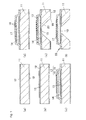
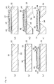
- the conventional capacitive vibration sensor is manufactured through steps as shown in Figs. 1(a) to 1(f) . The steps will be briefly described below.
- a Si substrate 11 surfaces of a Si substrate 11 are oxidized through a thermal oxidation method, and the surfaces of the Si substrate 11 is protected with a thermally oxidized film (SiO 2 film) 12.
- a vibration electrode plate 13 movable electrode plate
- a sacrifice layer 14 made of SiO 2 is deposited on the upper surface of the Si substrate 11 from above the vibration electrode plate 13, and the sacrifice layer 1.4 is etched to form a mesa type sacrifice layer 14.
- a back plate 15 is formed by depositing SiN on the upper surface of the Si substrate 11 from above the sacrifice layer 14, and then a fixed electrode 16 made of metal thin film is formed on the back plate 1, to form a fixed electrode plate 17 including the back plate 15 and the fixed electrode 16. Subsequently, as shown in Fig. 1 (d) , a plurality of acoustic perforations 18 is opened in the fixed electrode plate 17 by etching.
- a window 19 is opened in that thermally oxidized film 12 on the back surface side, and the Si substrate 11 is anisotropically etched from the window 19 to form a hollow part 20.
- the hollow part 20 is reached up to the upper surface of the Si substrate 11 to pass the hollow part 20 through the Si substrate 11.
- the sacrifice layer 14 is removed by etching through the hollow part 20 and the acoustic perforation 18, and a vibration electrode plate 13 that can vibrate is arranged in a space between the Si substrate 11 and the fixed electrode plate 17 to obtain a chip-shaped vibration sensor 23.
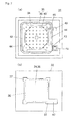
- Fig. 2(a) is a schematic plan view of a vibration sensor 23 manufactured as mentioned above
- Fig. 2(b) is a plan view showing a state in which the vibration electrode plate 13 is exposed by removing the fixed electrode plate 17.
- the reference numeral 24 indicates an electrode pad electrically conducted with the fixed electrode 16 of the fixed electrode plate 17
- the reference numeral 25 indicates an electrode pad electrically conducted with the vibration electrode plate 13.
- the vibration electrode plate 13 has the four corner portions formed as a supporting leg 26 fixed to the Si substrate 11.
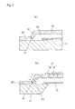
- Figs. 3(a) and 3(b) are views for describing the reason the strength of the side wall portion lowers in the manufacturing steps of the vibration sensor.
- Fig. 3(a) is a partially enlarged cross-sectional view of a state in which SiN is deposited on the mesa type sacrifice layer 14 to form the back plate 5, and shows the initial step of Fig. 1(c) .
- the film growth rate becomes greatest in a vertical direction, and thus the film thickness is greatest in a horizontal plane of the back plate 15 and the film thickness becomes thinner than the horizontal plane at the side wall portion 21, Furthermore, the film quality is worse at the side wall portion 21 than the horizontal plane.
- the hollow part 20 is formed by performing wet etching on the Si substrate 11 with TMAH and KOH solution or performing dry etching using XeF 2 gas.
- the back plate 15 is also simultaneously etched to some extent and particularly the thickness of the side wall portion 21 tends to be thin.
- the sacrifice layer 14 is removed by performing wet etching with hydrofluoric acid aqueous solution or performing dry etching using CF gas.
- the back plate 15 is also simultaneously etched to some extent and particularly the thickness of the side wall portion 21 tends to be thin.
- the stress has no place to escape when impact is externally applied to the vibration sensor 23, whereby the stress concentrates at the side wall portion 21 of the back plate 15 and the boundary of the side wall portion 21 and the fixed portion 22, thereby forming the crack in the back plate 15 and breaking the same.
- the strength of the back plate 15 can be increased by increasing the film thickness at the time of forming the back plate 15, but the productivity of the vibration sensor 23 worsens since the film forming time becomes longer and the processing accuracy of the back plate lowers with such a countermeasure method, and thus it is not practical.
- Patent Document 1 discloses a sensor in which the rigidity of the back plate (thin film plate of silicon nitride) is increased by forming the side wall portion of the back plate as a rib structure thereby preventing the warp of the back plate.
- the rib structure is formed at the side wall portion of the back plate, and thus the strength of the side wall portion appears to have increased.
- the side wall portion having the rib structure cannot prevent the etching of the back plate when etching the substrate and the sacrifice layer and cannot make the film quality of the side wall portion satisfactory when forming the back plate. Therefore, it is not effective in enhancing the strength of the side wall portion.
- the side wall portion has a rib structure, the stress rather tends to easily concentrate at the rib when impact is externally applied, thereby forming cracks at the side wall portion, the base portion thereof, and the like and breaking the same.
- the present invention has been devised to solve the problems described above, and an object thereof is to provide a capacitive sensor capable of enhancing the strength of a fixed electrode plate positioned on the outer side of a movable electrode plate and the fixed electrode plate configuring a capacitor, and increasing impact resistance and breakage resistance.
- a capacitive sensor of the present invention induces a substrate, a movable electrode plate arranged on an upper surface of the substrate, and a fixed electrode plate arranged on the upper surface of the substrate so as to cover the movable electrode plate, a physical amount or change thereof being detected by a capacitance or a change thereof between the movable electrode plate and the fixed electrode plate, wherein the fixed electrode plate has a portion facing the upper surface of the substrate through a space supported by a side wall portion arranged on an inner edge of a portion fixed to the upper surface of the substrate without interposing a space, and a reinforcement film is formed on at least one part of the side wall portion.
- the strength of the side wall portion of the fixed electrode plate can be enhanced by the reinforcement film since the reinforcement film is formed on the side wall portion positioned on the inner edge of the region fixed to the substrate of the fixed electrode plate.
- the fixed electrode plate is prevented from being etched with the substrate and the like in the region covered with the reinforcement film so that the thickness can be suppressed from becoming thin.
- the fixed electrode plate can be prevented from breaking by external impact etc., and the impact resistance and the breakage resistance of the capacitive sensor can be enhanced.
- the reinforcement film is made of metal, and the reinforcement film is electrically insulated with both the movable electrode plate and the fixed electrode plate.
- the reinforcement film can be simultaneously formed when forming the fixed electrode plate and other electrodes since the reinforcement film is made of metal, whereby the manufacturing steps of the capacitive sensor can be simplified.
- the metal with plasticity as the material of the reinforcement film enters into the crack and fills the crack when the reinforcement film is formed on the fixed electrode plate, and hence the cracks can be restored to a certain extent.
- the capacitance between the fixed electrode plate and the movable electrode plate is not adversely affected by forming the reinforcement film since the reinforcement film made of metal is not electrically conducted with the fixed electrode plate and the movable electrode plate.
- the reinforcement film is desirably formed by at least one material selected from Au, Cr, and Pt. Since Au, Cr, Pt has chemical resistance, the reinforcement film is less likely to be etched and to become thin in the etching step (e.g., etching step of substrate and sacrifice layer) after forming the reinforcement film by forming the reinforcement film with Au, Cr, Pt, and hence the strength of the reinforcement film is less likely to lower.
- the reinforcement film desirably does not overlap either an electrically conductive region of the movable electrode plate and an electrically conductive region of the fixed electrode plate. Since the reinforcement film made of metal does not overlap the electrically conductive region of the movable electrode plate and the electrically conductive region of the fixed electrode plate, parasitic capacitance is less likely to occur between the reinforcement film and the movable electrode plate and between the reinforcement film and the fixed electrode plate, whereby the lowering in sensitivity of the capacitive sensor due to parasitic capacitance can be suppressed.
- Another aspect of the capacitive sensor of the present invention includes arranging the reinforcement film on the outer surface of the side wall portion. Since the fixed electrode plate often has the outer peripheral part fixed to the substrate and the cracks and breakage of the fixed electrode plate tend to easily occur at the side wall portion of the fixed electrode plate, the cracks and breakage of the fixed electrode plate can be affectively prevented by arranging the reinforcement firm on the outer surface of the side wall portion according to this aspect. Furthermore, the reinforcement film can be formed at the same time as the fixed electrode of the fixed electrode plate since the reinforcement film is arranged on the outer surface of the fixed electrode plate, whereby the manufacturing steps of the capacitive sensor can be simplified,
- Still another aspect of the capacitive sensor of the present invention includes arranging the reinforcement film on the inner surface of the side wall portion.
- the fixed electrode plate often has the outer peripheral part fixed to the substrate and the cracks and breakage of the fixed electrode plate tend to easily occur at the side wall portion of the fixed electrode plate, the cracks and breakage of the fixed electrode plate can be affectively prevented by arranging the reinforcement film on the inner surface of the side wall portion according to this aspect.
- the reinforcement film is desirably formed entirely excluding a region for insulation adjacent to the region that does not overlap either the electrically conductive region of the movable electrode plate and the electrically conductive region of the fixed electrode plate on at least one of an outer surface and an inner surface of the side wall portions.
- the reinforcement film is desirably arranged at an area as wide as possible so as not to conduct with the fixed electrode plate and the movable electrode plate and so as not to overlap the electrically conductive region of the fixed electrode plate and the electrically conductive region of the movable electrode plate, whereby the strength of the side wall portion can be increased as much as possible.
- the means for solving the problems in the present invention may appropriately combine the configuring elements described above, and the present invention enables a great number of variations from the combinations of the configuring elements.
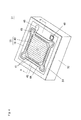
- FIG. 4 is a perspective view showing the vibration sensor 31 according to the first embodiment
- Fig. 5 is an exploded perspective view thereof.
- Fig. 6 is a schematic cross-sectional view taken along line X-X of Fig. 4 .
- Fig. 7(a) is a plan view schematically showing the vibration sensor of the first embodiment.
- Fig. 7(b) is a schematic plan view showing a state in which a fixed electrode plate is removed from the vibration sensor of Fig. 7(a) to expose the vibration electrode plate.
- the vibration sensor 31 is a capacitive sensor, where a vibration electrode plate 34 (movable electrode plate) is arranged on an upper surface of a silicon substrate 32 through an insulation coating 33, and a fixed electrode plate 35 is arranged thereon through a microscopic air gap (space).
- a vibration electrode plate 34 movable electrode plate
- the silicon substrate 32 includes a hollow part 36 including a square column shaped through-hole or a square truncated cone shaped recess (hollow part 36 passing through in an up and down direction is shown in the figure) the size of the silicon substrate 32 is 1 to 1.5 mm angle (may be smaller) in plan view, and the thickness of the silicon substrate 32 is about 400 to 500 ⁇ m).
- the upper surface of the silicon substrate 32 is formed with the insulation coating 33 made of oxide film (SiO 2 film) and the like.
- the vibration electrode plate 34 is formed by a polysilicon thin film having a film thickness of about 1 ⁇ m.
- the vibration electrode plate 34 is a thin film having a substantially rectangular shape, and supporting legs 37 extend toward the outside in a diagonal direction at the four corners.
- An extended part 47 is extended from one of the supporting legs 37.
- the vibration electrode plate 34 is arranged on the upper surface of the silicon substrate 32 so as to cover the upper surface of the hollow part 36, and supporting legs 37 at the four corners and the extended part 47 are fixed on the insulation coating 33.
- the portion of the vibration electrode plate 34 supported in air at the upper side of the hollow part 36 is a diaphragm 38 (vibration film), and vibrates in response to a sound pressure.
- the fixed electrode plate 35 has a fixed electrode 40 including a metal thin film arranged on an upper surface of a back plate 39 including a nitride film. As shown in Fig. 6 , the fixed electrode plate 35 covers the diaphragm 38 with a microscopic gap of about 3 ⁇ m in the region facing the diaphragm 38, and the fixed electrode 40 configures a capacitor facing the diaphragm 38.
- the outer peripheral part of the fixed electrode plate 35 that is, the portion on the outer side of the region facing the diaphragm 38 is fixed to the upper surface of the silicon substrate 32 through the insulation coating 33 including an oxide film and the like. Such a fixed portion is hereinafter referred to as a fixed part 42.
- a drawing portion 45 is extended from the fixed electrode 40, where an electrode pad 46 (Au film) electrically conducted with the fixed electrode 40 is arranged at the distal end of the drawing portion 45.
- An electrode pad 48 (Au film) that joins to the extended part 47 of the vibration electrode plate 34 to electrically conduct with the vibration electrode plate 34 is arranged on the fixed electrode plate 35.
- the electrode plate 46 is arranged on the upper surface of the back plate 39, and the electrode pad 48 is positioned in the opening of the back plate 39.
- the outer surface of the back plate 39 is covered with a reinforcement film 44 including a metal film at one part of the region along the inner peripheral edge of the fixed part 42.
- a plurality of acoustic perforations 41 (acoustic holes) for passing the sound pressure (vibration) is perforated in the fixed electrode 40 and the back plate 39 so as to pass through the upper surface to the lower surface.
- the vibration electrode plate 34 is a thin film of about 1 ⁇ m since is to vibrate in resonance with the sound pressure, but the fixed electrode plate 35 is an electrode that does not vibrate by the sound pressure, and thus is thick, that is, has a thickness of greater than or equal to 2 ⁇ m.
- the vibration sensor 31 when the acoustic vibration (compressional wave of air) enters from the front surface side, the acoustic vibration passes through the acoustic perforations 41 of the fixed electrode plate 35 and reaches the diaphragm 38, thereby vibrating the diaphragm 38.
- the diaphragm 38 vibrates, the gap distance between the diaphragm 38 and the fixed electrode plate 35 changes, whereby the capacitance between the diaphragm 38 and the fixed electrode 40 changes. Therefore, the vibration of the sound can be converted to an electric signal for detection by applying a direct current (DC) voltage between the electrode pads 46 and 48, and taking out the change in capacitance as an electric signal.
- DC direct current
- Figs. 7(a) and 7(b) show the structure shown in Fig. 4 and Fig. 5 in a simplified manner to facilitate the understanding of the basic structure of the first embodiment.
- the configuration of the reinforcement film 44 will be described with reference to Figs. 7(a) and 7(b) in place of Fig. 4 and Fig. 5 .
- a second and third embodiments to be described later will also be described with reference to the similarly simplified figures.
- the outer peripheral part of the back plate 39 that is, the fixed part 42 is fixed to the upper surface of the silicon substrate 32, where the region on the inner side thereof is floated from the upper surface of the silicon substrate 32 and faced to the vibration electrode plate 34.
- the space between the upper surface of the back plate 39 flouting from the silicon substrate 32 and the fixed part 42 is a side wall portion 43 inclined with respect to the horizontal surface,
- the fixed electrode plate 35 has the reinforcement film 44 formed at one part along the side wall portion 43 in the present embodiment since the strength of the side wall portion 43 tends to lower.
- the reinforcement film 44 preferably uses a material that is not etched (or with small etching rate) at the time of etching the silicon substrate 32, the sacrifice layer, and the like.
- the reinforcement film 44 also preferably uses a material that is less likely to break by impact, and thus preferably uses a material having ductility and toughness rather than a brittle material. Therefore, the reinforcement film 44 desirably uses a metal material, and in particular, preferably uses a material that is less likely to be corroded by the etchant such as Au, Cr, and Pt.
- the most preferably material of the reinforcement film 44 is Au film.
- the reason being the reinforcement film 44 can be simultaneously formed when forming the electrode pads 46, 48 by using the Au film.
- the Au film is a metal excelling in ductility, and is suited for the reinforcement film 44. Furthermore, the Au film excels in chemical resistance, and is less likely to be corroded by the etchant.
- the reinforcement film 44 desirably has a two layer structure of upper layer Au film/lower layer Cr film. Since the Cr film excels in adhesiveness with another material, the adhesion force of the Au film and the back plate 39 can be enhanced by using the Cr film for the lower. The Cr film also excels in chemical resistance.
- the Cr film excels in chemical resistance and adhesiveness with another material, the use of the Cr film alone is also suited for the reinforcement film 44.
- the reinforcement film 44 extends to the upper surface of the fixed part 42 and the back plate 39.
- the reinforcement film 44 extends to the upper surface of the fixed part 42 and the back plate 39.
- the bent portion of the upper end and the lower end of the side wall portion 43 where crack is likely to occur at the time of forming the back plate 39 is covered with the reinforcement film 44.
- the reinforcement film 44 is arranged at one part of the side wall portion 43 so as not to contact the electrically conductive region (fixed electrode 40, drawing portion 45, electrode pad 46) of the fixed electrode plate 35 and the electrically conductive region (vibration electrode plate 34 itself) of the vibration electrode plate 34, and so as not to overlap the electrically conductive region of the fixed electrode plate 35 and the electrically conductive region of the vibration electrode plate 34,
- the reinforcement film 44 desirably covers an area as wide as possible of the side wall portion 43 to an extent of not contacting and overlapping the electrically conductive regions of the fixed electrode plate 35 and the vibration electrode plate 34 so that the strength of the side wall portion 43 increases. That is, the reinforcement film 44 is desirably formed entirely excluding the region for insulation adjacent to the region that does not overlap the electrically conductive region of the vibration electrode plate 34 and the electrically conductive region of the fixed electrode plate 35 of the side wall portion 43.
- Fig. 9 is a cross-sectional view taken along line Y-Y of Fig. 8 .
- the reinforcement film 44 is arranged over the entire periphery of the side wall portion 43. As shown in the comparison example, if the reinforcement film 44 made of metal is passed through the drawing portion 45, the reinforcement film 44 contacts the drawing portion 45 thereby conducting the reinforcement film 44 and the fixed electrode plate 35, changing the characteristics of the vibration sensor 31, and towering the sensitivity.
- the vibration electrode plate 34 and the fixed electrode plate 35 short circuit by the reinforcement film 44, and hence the vibration sensor 31 becomes a defective product.
- the reinforcement film 44 is partially removed so that the reinforcement film 44 does not pass through the electrically conductive region of the vibration electrode plate 34 and the electrically conductive region of the fixed electrode plate 35, whereby drawbacks such as conduction of the reinforcement film 44 and the fixed electrode 40 etc., short circuit of the vibration electrode plate 34 and the fixed electrode plate 35, and generation of parasitic capacitance can be avoided, and the sensitivity and the properties of the vibration sensor 31 can be held satisfactorily.
- Fig. 10(a) to 10(f) The manufacturing method of the vibration sensor 31 of the first embodiment will be described by Fig. 10(a) to 10(f) .
- the surface of the silicon substrate 32 is oxidized through thermal oxidation method, and the surface of the silicon substrate 32 is covered with the insulation coating 33 (SiO 2 film).
- the vibration electrode plate 34 is formed by a polysilicon film on the insulation coating 33 at the upper surface of the silicon substrate 32.
- a sacrifice layer 49 made of SiO 2 is deposited on the upper surface of the silicon substrate 32 from above the vibration electrode plate 34, and the sacrifice layer 49 is etched to form a mesa type sacrifice layer 49.
- a back plate 39 is formed by depositing SiN on the upper surface of the Si substrate 32 from above the sacrifice layer 49, and then a fixed electrode 40 made of metal thin film is formed on the back plate 39 to form a fixed electrode plate 35 including the back plate 39 and the fixed electrode 40.
- the reinforcement film 44 is formed at the side wall portion 43 of the back plate 39 and the vicinity thereof through the sputtering method and the like. In this case, the fixed electrode 40 and the reinforcement film 44 can be simultaneously formed in one step if the fixed electrode 40 and the reinforcement film 44 are of the same material, whereby the manufacturing step can be simplified.
- a plurality of acoustic perforations 41 is opened in the fixed electrode plate 35 by etching.
- a window 50 is opened in the insulation coating 33 on the rear surface side, and the hollow part 36 is formed by anisotropically etching the silicon substrate 32 from the window 50.
- the hollow part 36 is then reached up to the upper surface of the silicon substrate 32 to penetrate the hollow part 36 in the silicon substrate 32. Then, as shown in Fig.
- the sacrifice layer 49 is removed by etching through the hollow part 36 and the acoustic perforation 41, and the vibration electrode plate 34 the can vibrate is arranged in a space between the silicon substrate 32 and the fixed electrode plate 35 to obtain a chip-shapes vibration sensor 31.
- the back plate 39 (especially, side wall portion 43 which strength easily lowers in the manufacturing step) can be reinforced by the reinforcement film 44 according to the above described structure.
- the side wall portion 43 can be prevented from being corroded by etching and the thickness from being thinned by covering the side wall portion 43 with the reinforcement film 44 having etching resistance property.
- the crack sometimes forms in the side wall portion 43 of the back plate 39 in the step of forming the back plate 39, the crack can be filled and restored with the metal of the reinforcement film 44 by forming the reinforcement film 44 made of metal which is the plastic material in the side wall portion 43.
- the mechanical strength of the back plate 39 thus can be enhanced by the reinforcement film 44, and hence the impact resistance and the breakage resistance of the vibration sensor 31 are enhanced and the durability and the lifespan of the vibration sensor 31 are enhanced.
- Fig. 11 is a schematic plan view showing a vibration sensor 51 according to a second embodiment of the present invention.
- the reinforcement films 44 are arranged only in the regions corresponding to the four corners of the side wall portion 43 in plan view of the side wall portion 43 of the back plate 39 and the region in the vicinity thereto.
- Fig. 11 is a view schematically showing the vibration sensor 51, where the four corners of the side wall portion 43 are actually expanded toward the outside in the diagonal direction in accordance with the supporting legs 37 of the vibration electrode plate 34, as apparent from Fig. 4 and Fig. 5 which are the detailed figures of the first embodiment.
- the four corners are the portions where the strength tends to lower in particular of the side wall portion 43.
- the second embodiment is an embodiment in which the reinforcement film 44 is formed in a minimum region of the side wall portion 43 where the strength tends to be lowest.
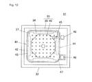
- Fig. 12 is a schematic plan view showing a vibration sensor 61 according to a third embodiment of the present invention.
- Fig. 13 is a schematic cross-sectional view of the vibration sensor 61 of the third embodiment.
- the reinforcement film 44 is arranged at the inner surface of the side wall portion 43 of the back plate 39 and the region in the vicinity thereof.
- the case of arranging the reinforcement film 44 on the inner surface of the side wall portion 43 is similar to the first embodiment in that the reinforcement film 44 is prevented from touching the electrically conductive region of the fixed electrode plate 35 and the electrically conductive region of the vibration electrode plate 34, and in that the reinforcement film 44 is prevented from overlapping the electrically conductive region of the fixed electrode plate 35 and the electrically conductive region of the vibration electrode plate 34. Since the reinforcement film 44 is arranged in the minimum region, the reinforcement film 44 may be arranged only at the four corners of the inner surface of the side wall portion 43.
- Figs. 14(a) to 14(f) are schematic cross-sectional views showing the manufacturing steps of the vibration sensor 61 of the third embodiment.
- the manufacturing steps are substantially the same as the manufacturing steps of the first embodiment shown in Fig. 10 .
- the difference is that the reinforcement film 44 is formed in advance on the side wall surface of the sacrifice layer 49 in Fig. 14(c) .
- the back plate 39 is formed on the sacrifice layer 49 as shown in Fig. 14(d) to form the reinforcement film 44 on the inner surface of the side wall portion 43 of the back plate 39.
- the side wall portion 43 can be protected by the reinforcement film 44 when removing the sacrifice layer 49 by etching as shown in Fig. 14(f) , and hence it is effective when the material of the back plate 39 has a relatively high etching rate with respect to the etchant used in the etching of the sacrifice layer 49.
- the reinforcement film 44 may be arranged on both sides, the inner surface and the outer surface, of the side wall portion 43.
Landscapes
- Engineering & Computer Science (AREA)
- Physics & Mathematics (AREA)
- Acoustics & Sound (AREA)
- Signal Processing (AREA)
- Mechanical Engineering (AREA)
- Computer Hardware Design (AREA)
- Microelectronics & Electronic Packaging (AREA)
- Pressure Sensors (AREA)
- Electrostatic, Electromagnetic, Magneto- Strictive, And Variable-Resistance Transducers (AREA)
Abstract
Description
- The present invention prelates to capacitive sensors, and in particular, to a capacitive sensor of a microscopic size manufactured using an MEMS (Micro Electro Mechanical System) technique or a micromachining technique.
- A capacitive sensor of a microscopic size is manufactured using an MEMS technique or a micromachining technique, as mentioned above. For example, the conventional capacitive vibration sensor (microphone) is manufactured through steps as shown in
Figs. 1(a) to 1(f) . The steps will be briefly described below. - First, as shown in
Fig. 1(a) , surfaces of aSi substrate 11 are oxidized through a thermal oxidation method, and the surfaces of theSi substrate 11 is protected with a thermally oxidized film (SiO2 film) 12. Then, as shown inFig. 1(b) , a vibration electrode plate 13 (movable electrode plate) is formed by a polysilicon film on the thermally oxidizedfilm 12 at an upper surface of theSi substrate 11. As shown inFig. 1(c) , asacrifice layer 14 made of SiO2 is deposited on the upper surface of theSi substrate 11 from above thevibration electrode plate 13, and the sacrifice layer 1.4 is etched to form a mesatype sacrifice layer 14. Furthermore, aback plate 15 is formed by depositing SiN on the upper surface of theSi substrate 11 from above thesacrifice layer 14, and then a fixedelectrode 16 made of metal thin film is formed on theback plate 1, to form afixed electrode plate 17 including theback plate 15 and thefixed electrode 16. Subsequently, as shown inFig. 1 (d) , a plurality ofacoustic perforations 18 is opened in thefixed electrode plate 17 by etching. - Thereafter, as shown in
Fig. 1 (e) , awindow 19 is opened in that thermally oxidizedfilm 12 on the back surface side, and theSi substrate 11 is anisotropically etched from thewindow 19 to form ahollow part 20. Thehollow part 20 is reached up to the upper surface of theSi substrate 11 to pass thehollow part 20 through theSi substrate 11. Then, as shown inFig. 1(f) , thesacrifice layer 14 is removed by etching through thehollow part 20 and theacoustic perforation 18, and avibration electrode plate 13 that can vibrate is arranged in a space between theSi substrate 11 and thefixed electrode plate 17 to obtain a chip-shaped vibration sensor 23. -
Fig. 2(a) is a schematic plan view of avibration sensor 23 manufactured as mentioned above, andFig. 2(b) is a plan view showing a state in which thevibration electrode plate 13 is exposed by removing thefixed electrode plate 17. Thereference numeral 24 indicates an electrode pad electrically conducted with thefixed electrode 16 of thefixed electrode plate 17, and thereference numeral 25 indicates an electrode pad electrically conducted with thevibration electrode plate 13. Thevibration electrode plate 13 has the four corner portions formed as a supportingleg 26 fixed to theSi substrate 11. - However, in the
conventional vibration sensor 23, the strength near a fixed portion of theback plate 15, in particular, the strength of a side wall portion raised from the end of the fixed portion easily lowers since it is formed as shown inFigs. 1(a) to 1(f) .Figs. 3(a) and 3(b) are views for describing the reason the strength of the side wall portion lowers in the manufacturing steps of the vibration sensor. -
Fig. 3(a) is a partially enlarged cross-sectional view of a state in which SiN is deposited on the mesatype sacrifice layer 14 to form the back plate 5, and shows the initial step ofFig. 1(c) . In the deposition step of SiN, the film growth rate becomes greatest in a vertical direction, and thus the film thickness is greatest in a horizontal plane of theback plate 15 and the film thickness becomes thinner than the horizontal plane at theside wall portion 21, Furthermore, the film quality is worse at theside wall portion 21 than the horizontal plane. - In the step of forming the
hollow part 20 ofFig. 1 (e) , thehollow part 20 is formed by performing wet etching on theSi substrate 11 with TMAH and KOH solution or performing dry etching using XeF2 gas. In this case, theback plate 15 is also simultaneously etched to some extent and particularly the thickness of theside wall portion 21 tends to be thin. - Furthermore, in the step of removing the
sacrifice layer 14 by etching ofFig. 1(f) , thesacrifice layer 14 is removed by performing wet etching with hydrofluoric acid aqueous solution or performing dry etching using CF gas. In this case, theback plate 15 is also simultaneously etched to some extent and particularly the thickness of theside wall portion 21 tends to be thin. - Thus, as a result of etching the
back plate 15 as indicated by arrows inFig. 3(b) , the thickness of theside wall portion 21 becomes thin and the film quality thereof also degrades, whereby the strength of theside wall portion 21 of theback plate 15 becomes lower than other areas. Furthermore, as shown inFig. 3(b) , a crack α tends to easily form at the boundary of thefixed portion 22 and theside wall portion 21 of theback plate 15 at the time of forming theback plate 15 and at the time of etching theSi substrate 11 and thesacrifice layer 14 - Thus, the stress has no place to escape when impact is externally applied to the
vibration sensor 23, whereby the stress concentrates at theside wall portion 21 of theback plate 15 and the boundary of theside wall portion 21 and thefixed portion 22, thereby forming the crack in theback plate 15 and breaking the same. - The strength of the
back plate 15 can be increased by increasing the film thickness at the time of forming theback plate 15, but the productivity of thevibration sensor 23 worsens since the film forming time becomes longer and the processing accuracy of the back plate lowers with such a countermeasure method, and thus it is not practical. -
Patent Document 1 discloses a sensor in which the rigidity of the back plate (thin film plate of silicon nitride) is increased by forming the side wall portion of the back plate as a rib structure thereby preventing the warp of the back plate. In such a structure, the rib structure is formed at the side wall portion of the back plate, and thus the strength of the side wall portion appears to have increased. - However, as in the above structure, the side wall portion having the rib structure cannot prevent the etching of the back plate when etching the substrate and the sacrifice layer and cannot make the film quality of the side wall portion satisfactory when forming the back plate. Therefore, it is not effective in enhancing the strength of the side wall portion.
- If the side wall portion has a rib structure, the stress rather tends to easily concentrate at the rib when impact is externally applied, thereby forming cracks at the side wall portion, the base portion thereof, and the like and breaking the same.
-
- Patent Document 1: Japanese Unexamined Patent Publication No.
2007-116721 Fig. 13 ,Fig. 14 ) - The present invention has been devised to solve the problems described above, and an object thereof is to provide a capacitive sensor capable of enhancing the strength of a fixed electrode plate positioned on the outer side of a movable electrode plate and the fixed electrode plate configuring a capacitor, and increasing impact resistance and breakage resistance.
- A capacitive sensor of the present invention induces a substrate, a movable electrode plate arranged on an upper surface of the substrate, and a fixed electrode plate arranged on the upper surface of the substrate so as to cover the movable electrode plate, a physical amount or change thereof being detected by a capacitance or a change thereof between the movable electrode plate and the fixed electrode plate, wherein the fixed electrode plate has a portion facing the upper surface of the substrate through a space supported by a side wall portion arranged on an inner edge of a portion fixed to the upper surface of the substrate without interposing a space, and a reinforcement film is formed on at least one part of the side wall portion.
- In the capacitive sensor of the present invention, the strength of the side wall portion of the fixed electrode plate can be enhanced by the reinforcement film since the reinforcement film is formed on the side wall portion positioned on the inner edge of the region fixed to the substrate of the fixed electrode plate. When etching the substrate and the like in the manufacturing steps of the capacitive sensor, the fixed electrode plate is prevented from being etched with the substrate and the like in the region covered with the reinforcement film so that the thickness can be suppressed from becoming thin. Thus, in the present invention, the fixed electrode plate can be prevented from breaking by external impact etc., and the impact resistance and the breakage resistance of the capacitive sensor can be enhanced.
- In one aspect of the capacitive sensor of the present invention, the reinforcement film is made of metal, and the reinforcement film is electrically insulated with both the movable electrode plate and the fixed electrode plate. According to such an aspect, the reinforcement film can be simultaneously formed when forming the fixed electrode plate and other electrodes since the reinforcement film is made of metal, whereby the manufacturing steps of the capacitive sensor can be simplified. Furthermore, even if cracks occur in the fixed electrode plate at the time of forming the fixed electrode plate, the metal with plasticity as the material of the reinforcement film enters into the crack and fills the crack when the reinforcement film is formed on the fixed electrode plate, and hence the cracks can be restored to a certain extent. Moreover, the capacitance between the fixed electrode plate and the movable electrode plate is not adversely affected by forming the reinforcement film since the reinforcement film made of metal is not electrically conducted with the fixed electrode plate and the movable electrode plate.
- The reinforcement film is desirably formed by at least one material selected from Au, Cr, and Pt. Since Au, Cr, Pt has chemical resistance, the reinforcement film is less likely to be etched and to become thin in the etching step (e.g., etching step of substrate and sacrifice layer) after forming the reinforcement film by forming the reinforcement film with Au, Cr, Pt, and hence the strength of the reinforcement film is less likely to lower.
- The reinforcement film desirably does not overlap either an electrically conductive region of the movable electrode plate and an electrically conductive region of the fixed electrode plate. Since the reinforcement film made of metal does not overlap the electrically conductive region of the movable electrode plate and the electrically conductive region of the fixed electrode plate, parasitic capacitance is less likely to occur between the reinforcement film and the movable electrode plate and between the reinforcement film and the fixed electrode plate, whereby the lowering in sensitivity of the capacitive sensor due to parasitic capacitance can be suppressed.
- Another aspect of the capacitive sensor of the present invention includes arranging the reinforcement film on the outer surface of the side wall portion. Since the fixed electrode plate often has the outer peripheral part fixed to the substrate and the cracks and breakage of the fixed electrode plate tend to easily occur at the side wall portion of the fixed electrode plate, the cracks and breakage of the fixed electrode plate can be affectively prevented by arranging the reinforcement firm on the outer surface of the side wall portion according to this aspect. Furthermore, the reinforcement film can be formed at the same time as the fixed electrode of the fixed electrode plate since the reinforcement film is arranged on the outer surface of the fixed electrode plate, whereby the manufacturing steps of the capacitive sensor can be simplified,
- Still another aspect of the capacitive sensor of the present invention includes arranging the reinforcement film on the inner surface of the side wall portion. As the fixed electrode plate often has the outer peripheral part fixed to the substrate and the cracks and breakage of the fixed electrode plate tend to easily occur at the side wall portion of the fixed electrode plate, the cracks and breakage of the fixed electrode plate can be affectively prevented by arranging the reinforcement film on the inner surface of the side wall portion according to this aspect.
- The reinforcement film is desirably formed entirely excluding a region for insulation adjacent to the region that does not overlap either the electrically conductive region of the movable electrode plate and the electrically conductive region of the fixed electrode plate on at least one of an outer surface and an inner surface of the side wall portions. The reinforcement film is desirably arranged at an area as wide as possible so as not to conduct with the fixed electrode plate and the movable electrode plate and so as not to overlap the electrically conductive region of the fixed electrode plate and the electrically conductive region of the movable electrode plate, whereby the strength of the side wall portion can be increased as much as possible.
- The means for solving the problems in the present invention may appropriately combine the configuring elements described above, and the present invention enables a great number of variations from the combinations of the configuring elements.
-
-
Figs. 1(a) to 1(f) are schematic cross-sectional views for describing manufacturing steps of a conventional capacitive vibration sensor. -
Fig. 2(a) is a schematic plan view of a vibration sensor manufactured by the steps ofFigs. 1(a) to 1(f) .Fig. 2(b) is a plan view showing a state in which the vibration electrode plate is exposed by removing the fixed electrode plate from the vibration sensor ofFig. 2(a) . -
Figs. 3(a) and 3(b) are views for describing the reason the strength of the fixed electrode plate lowers in the manufacturing steps of the vibration sensor. -
Fig. 4 is a perspective view showing a vibration sensor according to a first embodiment of the present invention. -
Fig. 5 is an exploded perspective view of the vibration sensor of the first embodiment. -
Fig. 6 is a schematic cross-sectional view taken along line X-X ofFig. 4 . -
Fig. 7(a) is a plan view schematically showing a vibration sensor of the first embodiment.Fig. 7(b) is a schematic plan view showing a state in which a fixed electrode plate is removed from the vibration sensor ofFig. 7(a) to expose the vibration electrode plate. -
Fig. 8 is a schematic plan view showing a vibration sensor of a comparison example. -
Fig. 9 is a cross-sectional view taken along line Y-Y ofFig. 8 . -
Figs. 10(a) to 10(f) are schematic cross-sectional views for describing manufacturing steps of the capacitive vibration sensor according to the first embodiment. -
Fig. 11 is a plan view schematically showing a vibration sensor according to a second embodiment of the present invention. -
Fig. 12 is a plan view schematically showing a vibration sensor according to a third embodiment of the present invention. -
Fig. 13 is a schematic cross-sectional view of the vibration sensor of the third embodiment. -
Figs. 14(a) to 14(f) are schematic cross-sectional views for describing manufacturing steps of a capacitive vibration sensor of the third embodiment. - The preferred embodiments of the present invention will be described blow with reference to the accompanying drawings. In the following embodiments, a capacitive vibration sensor (particularly, acoustic sensor), which is one type of capacitive sensor, will be described by way of example, but the present invention can be applied other than to the vibration sensor.
- A
vibration sensor 31 according to a first embodiment of the present invention will be described with reference toFig. 4 to Fig, 7 .Fig. 4 is a perspective view showing thevibration sensor 31 according to the first embodiment, andFig. 5 is an exploded perspective view thereof.Fig. 6 is a schematic cross-sectional view taken along line X-X ofFig. 4 .Fig. 7(a) is a plan view schematically showing the vibration sensor of the first embodiment.Fig. 7(b) is a schematic plan view showing a state in which a fixed electrode plate is removed from the vibration sensor ofFig. 7(a) to expose the vibration electrode plate. - The
vibration sensor 31 is a capacitive sensor, where a vibration electrode plate 34 (movable electrode plate) is arranged on an upper surface of asilicon substrate 32 through aninsulation coating 33, and a fixedelectrode plate 35 is arranged thereon through a microscopic air gap (space). - As shown in
Fig. 5 , thesilicon substrate 32 includes ahollow part 36 including a square column shaped through-hole or a square truncated cone shaped recess (hollow part 36 passing through in an up and down direction is shown in the figure) the size of thesilicon substrate 32 is 1 to 1.5 mm angle (may be smaller) in plan view, and the thickness of thesilicon substrate 32 is about 400 to 500 µm). The upper surface of thesilicon substrate 32 is formed with theinsulation coating 33 made of oxide film (SiO2 film) and the like. - The
vibration electrode plate 34 is formed by a polysilicon thin film having a film thickness of about 1 µm. Thevibration electrode plate 34 is a thin film having a substantially rectangular shape, and supportinglegs 37 extend toward the outside in a diagonal direction at the four corners. Anextended part 47 is extended from one of the supportinglegs 37. Thevibration electrode plate 34 is arranged on the upper surface of thesilicon substrate 32 so as to cover the upper surface of thehollow part 36, and supportinglegs 37 at the four corners and theextended part 47 are fixed on theinsulation coating 33. The portion of thevibration electrode plate 34 supported in air at the upper side of the hollow part 36 (portion other than the supportinglegs 37 and theextended part 47 in the present embodiment) is a diaphragm 38 (vibration film), and vibrates in response to a sound pressure. - The fixed
electrode plate 35 has a fixedelectrode 40 including a metal thin film arranged on an upper surface of aback plate 39 including a nitride film. As shown inFig. 6 , the fixedelectrode plate 35 covers thediaphragm 38 with a microscopic gap of about 3 µm in the region facing thediaphragm 38, and the fixedelectrode 40 configures a capacitor facing thediaphragm 38. The outer peripheral part of the fixedelectrode plate 35, that is, the portion on the outer side of the region facing thediaphragm 38 is fixed to the upper surface of thesilicon substrate 32 through theinsulation coating 33 including an oxide film and the like. Such a fixed portion is hereinafter referred to as afixed part 42. - A drawing
portion 45 is extended from the fixedelectrode 40, where an electrode pad 46 (Au film) electrically conducted with the fixedelectrode 40 is arranged at the distal end of the drawingportion 45. An electrode pad 48 (Au film) that joins to theextended part 47 of thevibration electrode plate 34 to electrically conduct with thevibration electrode plate 34 is arranged on the fixedelectrode plate 35. Theelectrode plate 46 is arranged on the upper surface of theback plate 39, and theelectrode pad 48 is positioned in the opening of theback plate 39. The outer surface of theback plate 39 is covered with areinforcement film 44 including a metal film at one part of the region along the inner peripheral edge of the fixedpart 42. - A plurality of acoustic perforations 41 (acoustic holes) for passing the sound pressure (vibration) is perforated in the fixed
electrode 40 and theback plate 39 so as to pass through the upper surface to the lower surface. Thevibration electrode plate 34 is a thin film of about 1 µm since is to vibrate in resonance with the sound pressure, but the fixedelectrode plate 35 is an electrode that does not vibrate by the sound pressure, and thus is thick, that is, has a thickness of greater than or equal to 2 µm. - In the
vibration sensor 31, when the acoustic vibration (compressional wave of air) enters from the front surface side, the acoustic vibration passes through theacoustic perforations 41 of the fixedelectrode plate 35 and reaches thediaphragm 38, thereby vibrating thediaphragm 38. When thediaphragm 38 vibrates, the gap distance between thediaphragm 38 and the fixedelectrode plate 35 changes, whereby the capacitance between thediaphragm 38 and the fixedelectrode 40 changes. Therefore, the vibration of the sound can be converted to an electric signal for detection by applying a direct current (DC) voltage between theelectrode pads -
Figs. 7(a) and 7(b) show the structure shown inFig. 4 andFig. 5 in a simplified manner to facilitate the understanding of the basic structure of the first embodiment. In the following, the configuration of thereinforcement film 44 will be described with reference toFigs. 7(a) and 7(b) in place ofFig. 4 andFig. 5 . A second and third embodiments to be described later will also be described with reference to the similarly simplified figures. - As shown in
Fig. 6 andFig. 7(a) , the outer peripheral part of theback plate 39, that is, the fixedpart 42 is fixed to the upper surface of thesilicon substrate 32, where the region on the inner side thereof is floated from the upper surface of thesilicon substrate 32 and faced to thevibration electrode plate 34. The space between the upper surface of theback plate 39 flouting from thesilicon substrate 32 and thefixed part 42 is aside wall portion 43 inclined with respect to the horizontal surface, As described in the background art, the fixedelectrode plate 35 has thereinforcement film 44 formed at one part along theside wall portion 43 in the present embodiment since the strength of theside wall portion 43 tends to lower. - The
reinforcement film 44 preferably uses a material that is not etched (or with small etching rate) at the time of etching thesilicon substrate 32, the sacrifice layer, and the like. Thereinforcement film 44 also preferably uses a material that is less likely to break by impact, and thus preferably uses a material having ductility and toughness rather than a brittle material. Therefore, thereinforcement film 44 desirably uses a metal material, and in particular, preferably uses a material that is less likely to be corroded by the etchant such as Au, Cr, and Pt. - The most preferably material of the
reinforcement film 44 is Au film. The reason being thereinforcement film 44 can be simultaneously formed when forming theelectrode pads reinforcement film 44. Furthermore, the Au film excels in chemical resistance, and is less likely to be corroded by the etchant. - Moreover, the
reinforcement film 44 desirably has a two layer structure of upper layer Au film/lower layer Cr film. Since the Cr film excels in adhesiveness with another material, the adhesion force of the Au film and theback plate 39 can be enhanced by using the Cr film for the lower. The Cr film also excels in chemical resistance. - Since the Cr film excels in chemical resistance and adhesiveness with another material, the use of the Cr film alone is also suited for the
reinforcement film 44. - The form of the
reinforcement film 44 will now be described. As shown inFig. 6 , thereinforcement film 44 extends to the upper surface of the fixedpart 42 and theback plate 39. In other words, the bent portion of the upper end and the lower end of theside wall portion 43 where crack is likely to occur at the time of forming theback plate 39 is covered with thereinforcement film 44. - As shown in
Fig. 7(a) , thereinforcement film 44 is arranged at one part of theside wall portion 43 so as not to contact the electrically conductive region (fixedelectrode 40, drawingportion 45, electrode pad 46) of the fixedelectrode plate 35 and the electrically conductive region (vibration electrode plate 34 itself) of thevibration electrode plate 34, and so as not to overlap the electrically conductive region of the fixedelectrode plate 35 and the electrically conductive region of thevibration electrode plate 34, Thereinforcement film 44 desirably covers an area as wide as possible of theside wall portion 43 to an extent of not contacting and overlapping the electrically conductive regions of the fixedelectrode plate 35 and thevibration electrode plate 34 so that the strength of theside wall portion 43 increases. That is, thereinforcement film 44 is desirably formed entirely excluding the region for insulation adjacent to the region that does not overlap the electrically conductive region of thevibration electrode plate 34 and the electrically conductive region of the fixedelectrode plate 35 of theside wall portion 43. - The reason the
reinforcement film 44 is arranged so as not to contact nor overlap the electrically conductive region of the fixedelectrode plate 35 and the electrically conductive region of thevibration electrode plate 34 will be described in comparison with a comparative example (undesired example) shown inFig. 8 andFig. 9. Fig. 9 is a cross-sectional view taken along line Y-Y ofFig. 8 . - In the comparison example shown in
Fig. 8 andFig. 9 , thereinforcement film 44 is arranged over the entire periphery of theside wall portion 43. As shown in the comparison example, if thereinforcement film 44 made of metal is passed through the drawingportion 45, thereinforcement film 44 contacts the drawingportion 45 thereby conducting thereinforcement film 44 and the fixedelectrode plate 35, changing the characteristics of thevibration sensor 31, and towering the sensitivity. - Furthermore, if the
reinforcement film 44 passing the upper side of theextended part 47 runs out to theelectrode pad 48 or theelectrode pad 48 contacts thereinforcement film 44 due to position shift of theelectrode pad 48, thevibration electrode plate 34 and the fixedelectrode plate 35 short circuit by thereinforcement film 44, and hence thevibration sensor 31 becomes a defective product. - Even if the
reinforcement film 44 does not contact theelectrode pad 48, a parasitic capacitance C generates between thereinforcement film 44 and thevibration electrode plate 34, as shown inFig. 9 , if thereinforcement film 44 passes the upper side of theextended part 47, and hence the sensor sensitivity may lower by the parasitic capacitance C. - In the
vibration sensor 31 of the present embodiment, on the other hand, thereinforcement film 44 is partially removed so that thereinforcement film 44 does not pass through the electrically conductive region of thevibration electrode plate 34 and the electrically conductive region of the fixedelectrode plate 35, whereby drawbacks such as conduction of thereinforcement film 44 and the fixedelectrode 40 etc., short circuit of thevibration electrode plate 34 and the fixedelectrode plate 35, and generation of parasitic capacitance can be avoided, and the sensitivity and the properties of thevibration sensor 31 can be held satisfactorily. - The manufacturing method of the
vibration sensor 31 of the first embodiment will be described byFig. 10(a) to 10(f) . First, as shown inFig. 10(a) , the surface of thesilicon substrate 32 is oxidized through thermal oxidation method, and the surface of thesilicon substrate 32 is covered with the insulation coating 33 (SiO2 film). Then, as shown inFig, 10(b) , thevibration electrode plate 34 is formed by a polysilicon film on theinsulation coating 33 at the upper surface of thesilicon substrate 32. As shown inFig, 10(c) , asacrifice layer 49 made of SiO2 is deposited on the upper surface of thesilicon substrate 32 from above thevibration electrode plate 34, and thesacrifice layer 49 is etched to form a mesatype sacrifice layer 49. Furthermore, aback plate 39 is formed by depositing SiN on the upper surface of theSi substrate 32 from above thesacrifice layer 49, and then a fixedelectrode 40 made of metal thin film is formed on theback plate 39 to form a fixedelectrode plate 35 including theback plate 39 and the fixedelectrode 40. Thereinforcement film 44 is formed at theside wall portion 43 of theback plate 39 and the vicinity thereof through the sputtering method and the like. In this case, the fixedelectrode 40 and thereinforcement film 44 can be simultaneously formed in one step if the fixedelectrode 40 and thereinforcement film 44 are of the same material, whereby the manufacturing step can be simplified. - As shown in
Fig. 1(d) , a plurality ofacoustic perforations 41 is opened in the fixedelectrode plate 35 by etching. Thereafter, as shown inFig. 10(e) , awindow 50 is opened in theinsulation coating 33 on the rear surface side, and thehollow part 36 is formed by anisotropically etching thesilicon substrate 32 from thewindow 50. Thehollow part 36 is then reached up to the upper surface of thesilicon substrate 32 to penetrate thehollow part 36 in thesilicon substrate 32. Then, as shown inFig. 10(f) , thesacrifice layer 49 is removed by etching through thehollow part 36 and theacoustic perforation 41, and thevibration electrode plate 34 the can vibrate is arranged in a space between thesilicon substrate 32 and the fixedelectrode plate 35 to obtain a chip-shapes vibration sensor 31. - In the
vibration sensor 31 of the present embodiment, the back plate 39 (especially,side wall portion 43 which strength easily lowers in the manufacturing step) can be reinforced by thereinforcement film 44 according to the above described structure. In the step of opening thehollow part 36 in thesilicon substrate 32 or in the step of removing thesacrifice layer 49 by etching, theside wall portion 43 can be prevented from being corroded by etching and the thickness from being thinned by covering theside wall portion 43 with thereinforcement film 44 having etching resistance property. Furthermore, although the crack sometimes forms in theside wall portion 43 of theback plate 39 in the step of forming theback plate 39, the crack can be filled and restored with the metal of thereinforcement film 44 by forming thereinforcement film 44 made of metal which is the plastic material in theside wall portion 43. The mechanical strength of theback plate 39 thus can be enhanced by thereinforcement film 44, and hence the impact resistance and the breakage resistance of thevibration sensor 31 are enhanced and the durability and the lifespan of thevibration sensor 31 are enhanced. -
Fig. 11 is a schematic plan view showing avibration sensor 51 according to a second embodiment of the present invention. In the present embodiment, thereinforcement films 44 are arranged only in the regions corresponding to the four corners of theside wall portion 43 in plan view of theside wall portion 43 of theback plate 39 and the region in the vicinity thereto. -
Fig. 11 is a view schematically showing thevibration sensor 51, where the four corners of theside wall portion 43 are actually expanded toward the outside in the diagonal direction in accordance with the supportinglegs 37 of thevibration electrode plate 34, as apparent fromFig. 4 andFig. 5 which are the detailed figures of the first embodiment. Thus, the four corners are the portions where the strength tends to lower in particular of theside wall portion 43. Thus, the second embodiment is an embodiment in which thereinforcement film 44 is formed in a minimum region of theside wall portion 43 where the strength tends to be lowest. -
Fig. 12 is a schematic plan view showing avibration sensor 61 according to a third embodiment of the present invention.Fig. 13 is a schematic cross-sectional view of thevibration sensor 61 of the third embodiment. In this embodiment, thereinforcement film 44 is arranged at the inner surface of theside wall portion 43 of theback plate 39 and the region in the vicinity thereof. - The case of arranging the
reinforcement film 44 on the inner surface of theside wall portion 43 is similar to the first embodiment in that thereinforcement film 44 is prevented from touching the electrically conductive region of the fixedelectrode plate 35 and the electrically conductive region of thevibration electrode plate 34, and in that thereinforcement film 44 is prevented from overlapping the electrically conductive region of the fixedelectrode plate 35 and the electrically conductive region of thevibration electrode plate 34. Since thereinforcement film 44 is arranged in the minimum region, thereinforcement film 44 may be arranged only at the four corners of the inner surface of theside wall portion 43. -
Figs. 14(a) to 14(f) are schematic cross-sectional views showing the manufacturing steps of thevibration sensor 61 of the third embodiment. The manufacturing steps are substantially the same as the manufacturing steps of the first embodiment shown inFig. 10 . The difference is that thereinforcement film 44 is formed in advance on the side wall surface of thesacrifice layer 49 inFig. 14(c) . After forming thereinforcement film 44, theback plate 39 is formed on thesacrifice layer 49 as shown inFig. 14(d) to form thereinforcement film 44 on the inner surface of theside wall portion 43 of theback plate 39. - In the embodiment, the
side wall portion 43 can be protected by thereinforcement film 44 when removing thesacrifice layer 49 by etching as shown inFig. 14(f) , and hence it is effective when the material of theback plate 39 has a relatively high etching rate with respect to the etchant used in the etching of thesacrifice layer 49. - It should be recognized that the
reinforcement film 44 may be arranged on both sides, the inner surface and the outer surface, of theside wall portion 43. -
- 31, 51, 61 vibration sensor
- 32 silicon substrate
- 34 vibration electrode plate
- 35 fixed electrode plate
- 37 supporting leg
- 38 diaphragm
- 39 back plate
- 40 fixed electrode
- 41 acoustic perforation
- 42 fixed part
- 43 side wall portion
- 44 reinforcement film
- 45 drawing portion
- 46 electrode pad
- 47 extended part
- 48 electrode pad
- 49 sacrifice layer
Claims (7)
- A capacitive sensor comprising a substrate, a movable electrode plate arranged on an upper surface of the substrate, and a fixed electrode plate (35) arranged on the upper surface of the substrate so as to cover the movable electrode plate,
a physical amount or change thereof being detected by a capacitance or a change thereof between the movable electrode plate and the fixed electrode plate (35), characterized in that
the fixed electrode plate (35) has a portion facing the upper surface of the substrate through a space supported by a side wall portion (43) arranged on an inner edge of a portion fixed to the upper surface of the substrate without interposing a space, and
a reinforcement film (44) is formed on at least one part of the side wall portion (43). - The capacitive sensor according to claim 1, characterized in that
the reinforcement film (44) is made of metal, and
the reinforcement film (44) is electrically insulated with both the movable electrode plate and the fixed electrode plate (35). - The capacitive sensor according to claim 2, characterized in that
the reinforcement film (44) is formed by at least one material selected from Au, Cr, and Pt. - The capacitive sensor according to claim 2, characterized in that
the reinforcement film (44) does not overlap an electrically conductive region of the movable electrode plate and an electrically conductive region of the fixed electrode plate (35). - The capacitive sensor according to claim 1, characterized in that
the reinforcement film (44) is arranged on an outer surface of the side wall portion (43). - The capacitive sensor according to claim 1, characterized in that
the reinforcement film (44) is arranged on an inner surface of the side wall portion (43). - The capacitive sensor according to claim 1, characterized in that
the reinforcement film (44) is formed entirely excluding a region for insulation adjacent to the region that does not overlap either the electrically conductive region of the movable electrode plate and the electrically conductive region of the fixed electrode plate (35) on at least one of an outer surface and an inner surface of the side wall portion (43).
Applications Claiming Priority (2)
| Application Number | Priority Date | Filing Date | Title |
|---|---|---|---|
| JP2008218149A JP4419103B1 (en) | 2008-08-27 | 2008-08-27 | Capacitance type vibration sensor |
| PCT/JP2009/000727 WO2010023776A1 (en) | 2008-08-27 | 2009-02-20 | Capacitive vibration sensor |
Publications (3)
| Publication Number | Publication Date |
|---|---|
| EP2328361A1 true EP2328361A1 (en) | 2011-06-01 |
| EP2328361A4 EP2328361A4 (en) | 2012-09-26 |
| EP2328361B1 EP2328361B1 (en) | 2015-04-08 |
Family
ID=41720963
Family Applications (1)
| Application Number | Title | Priority Date | Filing Date |
|---|---|---|---|
| EP09809435.2A Not-in-force EP2328361B1 (en) | 2008-08-27 | 2009-02-20 | Capacitive vibration sensor |
Country Status (6)
| Country | Link |
|---|---|
| US (1) | US8803257B2 (en) |
| EP (1) | EP2328361B1 (en) |
| JP (1) | JP4419103B1 (en) |
| KR (1) | KR101158236B1 (en) |
| CN (1) | CN102124755A (en) |
| WO (1) | WO2010023776A1 (en) |
Cited By (3)
| Publication number | Priority date | Publication date | Assignee | Title |
|---|---|---|---|---|
| EP2579617A4 (en) * | 2010-05-27 | 2013-04-17 | Omron Tateisi Electronics Co | Acoustic transducer, and microphone using the acoustic transducer |
| US9980052B2 (en) | 2011-11-14 | 2018-05-22 | Tdk Corporation | MEMS-microphone with reduced parasitic capacitance |
| GB2567251A (en) * | 2017-10-05 | 2019-04-10 | Cirrus Logic Int Semiconductor Ltd | MEMS devices and processes |
Families Citing this family (22)
| Publication number | Priority date | Publication date | Assignee | Title |
|---|---|---|---|---|
| KR101113366B1 (en) * | 2008-02-20 | 2012-03-02 | 오므론 가부시키가이샤 | Electrostatic capacitive vibrating sensor |
| JP5374077B2 (en) | 2008-06-16 | 2013-12-25 | ローム株式会社 | MEMS sensor |
| JP2010098518A (en) * | 2008-10-16 | 2010-04-30 | Rohm Co Ltd | Method of manufacturing mems sensor, and mems sensor |
| JP5454345B2 (en) * | 2010-05-11 | 2014-03-26 | オムロン株式会社 | Acoustic sensor and manufacturing method thereof |
| DE102011002457A1 (en) * | 2011-01-05 | 2012-07-05 | Robert Bosch Gmbh | Micromechanical microphone device and method for producing a micromechanical microphone device |
| JP5872163B2 (en) | 2011-01-07 | 2016-03-01 | オムロン株式会社 | Acoustic transducer and microphone using the acoustic transducer |
| US9380380B2 (en) | 2011-01-07 | 2016-06-28 | Stmicroelectronics S.R.L. | Acoustic transducer and interface circuit |
| US8737674B2 (en) | 2011-02-11 | 2014-05-27 | Infineon Technologies Ag | Housed loudspeaker array |
| JP4924853B1 (en) * | 2011-02-23 | 2012-04-25 | オムロン株式会社 | Acoustic sensor and microphone |
| JP5338825B2 (en) * | 2011-02-23 | 2013-11-13 | オムロン株式会社 | Acoustic sensor and microphone |
| JP5861497B2 (en) * | 2012-02-29 | 2016-02-16 | オムロン株式会社 | Sensor device |
| JP5252104B1 (en) * | 2012-05-31 | 2013-07-31 | オムロン株式会社 | Capacitive sensor, acoustic sensor and microphone |
| KR101764226B1 (en) * | 2012-08-29 | 2017-08-04 | 한국전자통신연구원 | Mems acoustic sensor and fabrication method thereof |
| JP5987572B2 (en) | 2012-09-11 | 2016-09-07 | オムロン株式会社 | Acoustic transducer |
| JP6028479B2 (en) * | 2012-09-14 | 2016-11-16 | オムロン株式会社 | Capacitive sensor, acoustic sensor and microphone |
| US9681234B2 (en) * | 2013-05-09 | 2017-06-13 | Shanghai Ic R&D Center Co., Ltd | MEMS microphone structure and method of manufacturing the same |
| CN104980860A (en) * | 2014-04-10 | 2015-10-14 | 美商楼氏电子有限公司 | Reinforced backplate and method for using the backplate to an acoustic device |
| US20160117015A1 (en) * | 2014-10-28 | 2016-04-28 | Stmicroelectronics S.R.L. | Microelectromechanical vibration sensor |
| CN108810773A (en) * | 2017-04-26 | 2018-11-13 | 中芯国际集成电路制造(上海)有限公司 | microphone and its manufacturing method |
| KR102165882B1 (en) | 2018-12-28 | 2020-10-14 | 주식회사 제이피드림 | Thin film package and method of forming the same |
| KR102177143B1 (en) | 2020-04-27 | 2020-11-10 | 주식회사 제이피드림 | Thin film hermetic sealing package having cavity and method of forming the same |
| CN113613153B (en) * | 2021-08-27 | 2023-03-14 | 歌尔微电子股份有限公司 | Back electrode plate and microphone |
Family Cites Families (7)
| Publication number | Priority date | Publication date | Assignee | Title |
|---|---|---|---|---|
| KR100571967B1 (en) | 2000-08-11 | 2006-04-18 | 노우레스 일렉트로닉스, 엘엘시 | Mini broadband converter |
| JP2002209298A (en) | 2001-01-11 | 2002-07-26 | Seiko Epson Corp | Method for manufacturing condenser microphone, condenser microphone, and electronic device |
| CN1728888A (en) * | 2004-07-30 | 2006-02-01 | 三洋电机株式会社 | Acoustic sensor |
| JP2006121465A (en) | 2004-10-22 | 2006-05-11 | Sanyo Electric Co Ltd | Acoustic sensor and method for manufacturing acoustic sensor |
| KR100661347B1 (en) * | 2004-10-27 | 2006-12-27 | 삼성전자주식회사 | Micro thin film structure and MEMS switch using the same and method for manufacturing them |
| JP2007067893A (en) | 2005-08-31 | 2007-03-15 | Sanyo Electric Co Ltd | Acoustical sensor |
| US20070045757A1 (en) * | 2005-08-31 | 2007-03-01 | Sanyo Electric Co., Ltd. | Sensor |
-
2008
- 2008-08-27 JP JP2008218149A patent/JP4419103B1/en not_active Expired - Fee Related
-
2009
- 2009-02-20 WO PCT/JP2009/000727 patent/WO2010023776A1/en not_active Ceased
- 2009-02-20 EP EP09809435.2A patent/EP2328361B1/en not_active Not-in-force
- 2009-02-20 US US13/060,075 patent/US8803257B2/en active Active
- 2009-02-20 KR KR1020117001975A patent/KR101158236B1/en active Active
- 2009-02-20 CN CN2009801319295A patent/CN102124755A/en active Pending
Cited By (6)
| Publication number | Priority date | Publication date | Assignee | Title |
|---|---|---|---|---|
| EP2579617A4 (en) * | 2010-05-27 | 2013-04-17 | Omron Tateisi Electronics Co | Acoustic transducer, and microphone using the acoustic transducer |
| US8861753B2 (en) | 2010-05-27 | 2014-10-14 | Omron Corporation | Acoustic transducer, and microphone using the acoustic transducer |
| US9980052B2 (en) | 2011-11-14 | 2018-05-22 | Tdk Corporation | MEMS-microphone with reduced parasitic capacitance |
| GB2567251A (en) * | 2017-10-05 | 2019-04-10 | Cirrus Logic Int Semiconductor Ltd | MEMS devices and processes |
| US10623852B2 (en) | 2017-10-05 | 2020-04-14 | Cirrus Logic, Inc. | MEMS devices and processes |
| GB2567251B (en) * | 2017-10-05 | 2021-10-27 | Cirrus Logic Int Semiconductor Ltd | MEMS devices and processes |
Also Published As
| Publication number | Publication date |
|---|---|
| JP4419103B1 (en) | 2010-02-24 |
| EP2328361A4 (en) | 2012-09-26 |
| CN102124755A (en) | 2011-07-13 |
| US20110140213A1 (en) | 2011-06-16 |
| EP2328361B1 (en) | 2015-04-08 |
| US8803257B2 (en) | 2014-08-12 |
| JP2010056745A (en) | 2010-03-11 |
| KR101158236B1 (en) | 2012-06-19 |
| KR20110022717A (en) | 2011-03-07 |
| WO2010023776A1 (en) | 2010-03-04 |
Similar Documents
| Publication | Publication Date | Title |
|---|---|---|
| EP2328361B1 (en) | Capacitive vibration sensor | |
| EP2386521B1 (en) | Acoustic sensor having protective film and method of manufacturing the same | |
| JP5083369B2 (en) | Acoustic sensor and manufacturing method thereof | |
| KR101787187B1 (en) | System and method for a microphone | |
| EP2315457B1 (en) | Capacitance type vibration sensor | |
| JP4144640B2 (en) | Method for manufacturing vibration sensor | |
| US8098870B2 (en) | Silicon microphone | |
| JP2014090514A (en) | Device with micromechanical microphone structure and manufacturing method of device with micromechanical microphone structure | |
| JP6390423B2 (en) | Acoustic sensor and acoustic sensor manufacturing method | |
| KR20130039504A (en) | Mems microphone and manufacturing method thereof | |
| JP2007295487A (en) | Microphone manufacturing method | |
| US10469957B2 (en) | Capacitive transducer and acoustic sensor | |
| JP4273438B2 (en) | microphone | |
| EP3328093A1 (en) | Mems microphone having reduced leakage current and method of manufacturing the same |
Legal Events
| Date | Code | Title | Description |
|---|---|---|---|
| PUAI | Public reference made under article 153(3) epc to a published international application that has entered the european phase |
Free format text: ORIGINAL CODE: 0009012 |
|
| 17P | Request for examination filed |
Effective date: 20110317 |
|
| AK | Designated contracting states |
Kind code of ref document: A1 Designated state(s): AT BE BG CH CY CZ DE DK EE ES FI FR GB GR HR HU IE IS IT LI LT LU LV MC MK MT NL NO PL PT RO SE SI SK TR |
|
| AX | Request for extension of the european patent |
Extension state: AL BA RS |
|
| DAX | Request for extension of the european patent (deleted) | ||
| A4 | Supplementary search report drawn up and despatched |
Effective date: 20120823 |
|
| RIC1 | Information provided on ipc code assigned before grant |
Ipc: H04R 19/04 20060101AFI20120817BHEP |
|
| GRAP | Despatch of communication of intention to grant a patent |
Free format text: ORIGINAL CODE: EPIDOSNIGR1 |
|
| INTG | Intention to grant announced |
Effective date: 20140919 |
|
| GRAS | Grant fee paid |
Free format text: ORIGINAL CODE: EPIDOSNIGR3 |
|
| GRAA | (expected) grant |
Free format text: ORIGINAL CODE: 0009210 |
|
| AK | Designated contracting states |
Kind code of ref document: B1 Designated state(s): AT BE BG CH CY CZ DE DK EE ES FI FR GB GR HR HU IE IS IT LI LT LU LV MC MK MT NL NO PL PT RO SE SI SK TR |
|
| REG | Reference to a national code |
Ref country code: GB Ref legal event code: FG4D |
|
| REG | Reference to a national code |
Ref country code: CH Ref legal event code: EP |
|
| REG | Reference to a national code |
Ref country code: IE Ref legal event code: FG4D |
|
| REG | Reference to a national code |
Ref country code: AT Ref legal event code: REF Ref document number: 721333 Country of ref document: AT Kind code of ref document: T Effective date: 20150515 |
|
| REG | Reference to a national code |
Ref country code: DE Ref legal event code: R096 Ref document number: 602009030568 Country of ref document: DE Effective date: 20150521 |
|
| REG | Reference to a national code |
Ref country code: AT Ref legal event code: MK05 Ref document number: 721333 Country of ref document: AT Kind code of ref document: T Effective date: 20150408 |
|
| REG | Reference to a national code |
Ref country code: NL Ref legal event code: VDEP Effective date: 20150408 |
|
| REG | Reference to a national code |
Ref country code: LT Ref legal event code: MG4D |
|
| PG25 | Lapsed in a contracting state [announced via postgrant information from national office to epo] |
Ref country code: NL Free format text: LAPSE BECAUSE OF FAILURE TO SUBMIT A TRANSLATION OF THE DESCRIPTION OR TO PAY THE FEE WITHIN THE PRESCRIBED TIME-LIMIT Effective date: 20150408 |
|
| PG25 | Lapsed in a contracting state [announced via postgrant information from national office to epo] |
Ref country code: HR Free format text: LAPSE BECAUSE OF FAILURE TO SUBMIT A TRANSLATION OF THE DESCRIPTION OR TO PAY THE FEE WITHIN THE PRESCRIBED TIME-LIMIT Effective date: 20150408 Ref country code: FI Free format text: LAPSE BECAUSE OF FAILURE TO SUBMIT A TRANSLATION OF THE DESCRIPTION OR TO PAY THE FEE WITHIN THE PRESCRIBED TIME-LIMIT Effective date: 20150408 Ref country code: LT Free format text: LAPSE BECAUSE OF FAILURE TO SUBMIT A TRANSLATION OF THE DESCRIPTION OR TO PAY THE FEE WITHIN THE PRESCRIBED TIME-LIMIT Effective date: 20150408 Ref country code: NO Free format text: LAPSE BECAUSE OF FAILURE TO SUBMIT A TRANSLATION OF THE DESCRIPTION OR TO PAY THE FEE WITHIN THE PRESCRIBED TIME-LIMIT Effective date: 20150708 Ref country code: PT Free format text: LAPSE BECAUSE OF FAILURE TO SUBMIT A TRANSLATION OF THE DESCRIPTION OR TO PAY THE FEE WITHIN THE PRESCRIBED TIME-LIMIT Effective date: 20150810 Ref country code: ES Free format text: LAPSE BECAUSE OF FAILURE TO SUBMIT A TRANSLATION OF THE DESCRIPTION OR TO PAY THE FEE WITHIN THE PRESCRIBED TIME-LIMIT Effective date: 20150408 |
|
| PG25 | Lapsed in a contracting state [announced via postgrant information from national office to epo] |
Ref country code: LV Free format text: LAPSE BECAUSE OF FAILURE TO SUBMIT A TRANSLATION OF THE DESCRIPTION OR TO PAY THE FEE WITHIN THE PRESCRIBED TIME-LIMIT Effective date: 20150408 Ref country code: IS Free format text: LAPSE BECAUSE OF FAILURE TO SUBMIT A TRANSLATION OF THE DESCRIPTION OR TO PAY THE FEE WITHIN THE PRESCRIBED TIME-LIMIT Effective date: 20150808 Ref country code: GR Free format text: LAPSE BECAUSE OF FAILURE TO SUBMIT A TRANSLATION OF THE DESCRIPTION OR TO PAY THE FEE WITHIN THE PRESCRIBED TIME-LIMIT Effective date: 20150709 Ref country code: AT Free format text: LAPSE BECAUSE OF FAILURE TO SUBMIT A TRANSLATION OF THE DESCRIPTION OR TO PAY THE FEE WITHIN THE PRESCRIBED TIME-LIMIT Effective date: 20150408 |
|
| REG | Reference to a national code |
Ref country code: DE Ref legal event code: R097 Ref document number: 602009030568 Country of ref document: DE |
|
| PG25 | Lapsed in a contracting state [announced via postgrant information from national office to epo] |
Ref country code: DK Free format text: LAPSE BECAUSE OF FAILURE TO SUBMIT A TRANSLATION OF THE DESCRIPTION OR TO PAY THE FEE WITHIN THE PRESCRIBED TIME-LIMIT Effective date: 20150408 Ref country code: EE Free format text: LAPSE BECAUSE OF FAILURE TO SUBMIT A TRANSLATION OF THE DESCRIPTION OR TO PAY THE FEE WITHIN THE PRESCRIBED TIME-LIMIT Effective date: 20150408 |
|
| PLBE | No opposition filed within time limit |
Free format text: ORIGINAL CODE: 0009261 |
|
| STAA | Information on the status of an ep patent application or granted ep patent |
Free format text: STATUS: NO OPPOSITION FILED WITHIN TIME LIMIT |
|
| PG25 | Lapsed in a contracting state [announced via postgrant information from national office to epo] |
Ref country code: SK Free format text: LAPSE BECAUSE OF FAILURE TO SUBMIT A TRANSLATION OF THE DESCRIPTION OR TO PAY THE FEE WITHIN THE PRESCRIBED TIME-LIMIT Effective date: 20150408 Ref country code: RO Free format text: LAPSE BECAUSE OF NON-PAYMENT OF DUE FEES Effective date: 20150408 Ref country code: CZ Free format text: LAPSE BECAUSE OF FAILURE TO SUBMIT A TRANSLATION OF THE DESCRIPTION OR TO PAY THE FEE WITHIN THE PRESCRIBED TIME-LIMIT Effective date: 20150408 Ref country code: PL Free format text: LAPSE BECAUSE OF FAILURE TO SUBMIT A TRANSLATION OF THE DESCRIPTION OR TO PAY THE FEE WITHIN THE PRESCRIBED TIME-LIMIT Effective date: 20150408 |
|
| 26N | No opposition filed |
Effective date: 20160111 |
|
| PG25 | Lapsed in a contracting state [announced via postgrant information from national office to epo] |
Ref country code: IT Free format text: LAPSE BECAUSE OF FAILURE TO SUBMIT A TRANSLATION OF THE DESCRIPTION OR TO PAY THE FEE WITHIN THE PRESCRIBED TIME-LIMIT Effective date: 20150408 |
|
| PG25 | Lapsed in a contracting state [announced via postgrant information from national office to epo] |
Ref country code: BE Free format text: LAPSE BECAUSE OF NON-PAYMENT OF DUE FEES Effective date: 20160229 Ref country code: SI Free format text: LAPSE BECAUSE OF FAILURE TO SUBMIT A TRANSLATION OF THE DESCRIPTION OR TO PAY THE FEE WITHIN THE PRESCRIBED TIME-LIMIT Effective date: 20150408 |
|
| PG25 | Lapsed in a contracting state [announced via postgrant information from national office to epo] |
Ref country code: BE Free format text: LAPSE BECAUSE OF FAILURE TO SUBMIT A TRANSLATION OF THE DESCRIPTION OR TO PAY THE FEE WITHIN THE PRESCRIBED TIME-LIMIT Effective date: 20150408 |
|
| PG25 | Lapsed in a contracting state [announced via postgrant information from national office to epo] |
Ref country code: MC Free format text: LAPSE BECAUSE OF FAILURE TO SUBMIT A TRANSLATION OF THE DESCRIPTION OR TO PAY THE FEE WITHIN THE PRESCRIBED TIME-LIMIT Effective date: 20150408 Ref country code: LU Free format text: LAPSE BECAUSE OF FAILURE TO SUBMIT A TRANSLATION OF THE DESCRIPTION OR TO PAY THE FEE WITHIN THE PRESCRIBED TIME-LIMIT Effective date: 20160220 |
|
| REG | Reference to a national code |
Ref country code: CH Ref legal event code: PL |
|
| GBPC | Gb: european patent ceased through non-payment of renewal fee |
Effective date: 20160220 |
|
| PG25 | Lapsed in a contracting state [announced via postgrant information from national office to epo] |
Ref country code: CH Free format text: LAPSE BECAUSE OF NON-PAYMENT OF DUE FEES Effective date: 20160229 Ref country code: LI Free format text: LAPSE BECAUSE OF NON-PAYMENT OF DUE FEES Effective date: 20160229 |
|
| REG | Reference to a national code |
Ref country code: FR Ref legal event code: ST Effective date: 20161028 |
|
| REG | Reference to a national code |
Ref country code: IE Ref legal event code: MM4A |
|
| PG25 | Lapsed in a contracting state [announced via postgrant information from national office to epo] |
Ref country code: IE Free format text: LAPSE BECAUSE OF NON-PAYMENT OF DUE FEES Effective date: 20160220 Ref country code: FR Free format text: LAPSE BECAUSE OF NON-PAYMENT OF DUE FEES Effective date: 20160229 Ref country code: GB Free format text: LAPSE BECAUSE OF NON-PAYMENT OF DUE FEES Effective date: 20160220 |
|
| PG25 | Lapsed in a contracting state [announced via postgrant information from national office to epo] |
Ref country code: SE Free format text: LAPSE BECAUSE OF FAILURE TO SUBMIT A TRANSLATION OF THE DESCRIPTION OR TO PAY THE FEE WITHIN THE PRESCRIBED TIME-LIMIT Effective date: 20150408 |
|
| PG25 | Lapsed in a contracting state [announced via postgrant information from national office to epo] |
Ref country code: MT Free format text: LAPSE BECAUSE OF FAILURE TO SUBMIT A TRANSLATION OF THE DESCRIPTION OR TO PAY THE FEE WITHIN THE PRESCRIBED TIME-LIMIT Effective date: 20150408 |
|
| PG25 | Lapsed in a contracting state [announced via postgrant information from national office to epo] |
Ref country code: HU Free format text: LAPSE BECAUSE OF FAILURE TO SUBMIT A TRANSLATION OF THE DESCRIPTION OR TO PAY THE FEE WITHIN THE PRESCRIBED TIME-LIMIT; INVALID AB INITIO Effective date: 20090220 Ref country code: CY Free format text: LAPSE BECAUSE OF FAILURE TO SUBMIT A TRANSLATION OF THE DESCRIPTION OR TO PAY THE FEE WITHIN THE PRESCRIBED TIME-LIMIT Effective date: 20150408 |
|
| PG25 | Lapsed in a contracting state [announced via postgrant information from national office to epo] |
Ref country code: MT Free format text: LAPSE BECAUSE OF FAILURE TO SUBMIT A TRANSLATION OF THE DESCRIPTION OR TO PAY THE FEE WITHIN THE PRESCRIBED TIME-LIMIT Effective date: 20160229 Ref country code: MK Free format text: LAPSE BECAUSE OF FAILURE TO SUBMIT A TRANSLATION OF THE DESCRIPTION OR TO PAY THE FEE WITHIN THE PRESCRIBED TIME-LIMIT Effective date: 20150408 Ref country code: TR Free format text: LAPSE BECAUSE OF FAILURE TO SUBMIT A TRANSLATION OF THE DESCRIPTION OR TO PAY THE FEE WITHIN THE PRESCRIBED TIME-LIMIT Effective date: 20150408 |
|
| PG25 | Lapsed in a contracting state [announced via postgrant information from national office to epo] |
Ref country code: BG Free format text: LAPSE BECAUSE OF FAILURE TO SUBMIT A TRANSLATION OF THE DESCRIPTION OR TO PAY THE FEE WITHIN THE PRESCRIBED TIME-LIMIT Effective date: 20150408 |
|
| REG | Reference to a national code |
Ref country code: DE Ref legal event code: R081 Ref document number: 602009030568 Country of ref document: DE Owner name: MMI SEMICONDUCTOR CO., LTD., JP Free format text: FORMER OWNER: OMRON CORP., KYOTO-SHI, JP |
|
| PGFP | Annual fee paid to national office [announced via postgrant information from national office to epo] |
Ref country code: DE Payment date: 20231228 Year of fee payment: 16 |
|
| REG | Reference to a national code |
Ref country code: DE Ref legal event code: R119 Ref document number: 602009030568 Country of ref document: DE |
|
| PG25 | Lapsed in a contracting state [announced via postgrant information from national office to epo] |
Ref country code: DE Free format text: LAPSE BECAUSE OF NON-PAYMENT OF DUE FEES Effective date: 20250902 |