EP2327980A1 - Palladium ink exhaust sensor - Google Patents
Palladium ink exhaust sensor Download PDFInfo
- Publication number
- EP2327980A1 EP2327980A1 EP10190606A EP10190606A EP2327980A1 EP 2327980 A1 EP2327980 A1 EP 2327980A1 EP 10190606 A EP10190606 A EP 10190606A EP 10190606 A EP10190606 A EP 10190606A EP 2327980 A1 EP2327980 A1 EP 2327980A1
- Authority
- EP
- European Patent Office
- Prior art keywords
- ceramic
- sheet
- palladium
- exhaust sensor
- sensor
- Prior art date
- Legal status (The legal status is an assumption and is not a legal conclusion. Google has not performed a legal analysis and makes no representation as to the accuracy of the status listed.)
- Withdrawn
Links
- KDLHZDBZIXYQEI-UHFFFAOYSA-N Palladium Chemical compound [Pd] KDLHZDBZIXYQEI-UHFFFAOYSA-N 0.000 title claims abstract description 97
- 229910052763 palladium Inorganic materials 0.000 title claims abstract description 48
- 239000000919 ceramic Substances 0.000 claims abstract description 59
- 238000000034 method Methods 0.000 claims abstract description 30
- 239000011800 void material Substances 0.000 claims abstract description 10
- 229910003445 palladium oxide Inorganic materials 0.000 claims abstract description 9
- JQPTYAILLJKUCY-UHFFFAOYSA-N palladium(ii) oxide Chemical compound [O-2].[Pd+2] JQPTYAILLJKUCY-UHFFFAOYSA-N 0.000 claims abstract description 9
- 238000013022 venting Methods 0.000 claims description 27
- PNEYBMLMFCGWSK-UHFFFAOYSA-N aluminium oxide Inorganic materials [O-2].[O-2].[O-2].[Al+3].[Al+3] PNEYBMLMFCGWSK-UHFFFAOYSA-N 0.000 claims description 10
- OKTJSMMVPCPJKN-UHFFFAOYSA-N Carbon Chemical compound [C] OKTJSMMVPCPJKN-UHFFFAOYSA-N 0.000 claims description 7
- 229910052799 carbon Inorganic materials 0.000 claims description 7
- 238000007639 printing Methods 0.000 claims description 7
- 238000004519 manufacturing process Methods 0.000 claims description 5
- 238000010030 laminating Methods 0.000 claims description 3
- 238000007789 sealing Methods 0.000 claims description 3
- 238000010304 firing Methods 0.000 abstract description 20
- 238000004891 communication Methods 0.000 abstract description 4
- 239000010410 layer Substances 0.000 description 81
- 239000000976 ink Substances 0.000 description 39
- BASFCYQUMIYNBI-UHFFFAOYSA-N platinum Chemical compound [Pt] BASFCYQUMIYNBI-UHFFFAOYSA-N 0.000 description 24
- 229910052697 platinum Inorganic materials 0.000 description 12
- 239000011241 protective layer Substances 0.000 description 10
- MCMNRKCIXSYSNV-UHFFFAOYSA-N Zirconium dioxide Chemical compound O=[Zr]=O MCMNRKCIXSYSNV-UHFFFAOYSA-N 0.000 description 8
- 238000003475 lamination Methods 0.000 description 7
- 229910052751 metal Inorganic materials 0.000 description 7
- 239000002184 metal Substances 0.000 description 7
- 239000000463 material Substances 0.000 description 6
- WYTGDNHDOZPMIW-RCBQFDQVSA-N alstonine Natural products C1=CC2=C3C=CC=CC3=NC2=C2N1C[C@H]1[C@H](C)OC=C(C(=O)OC)[C@H]1C2 WYTGDNHDOZPMIW-RCBQFDQVSA-N 0.000 description 5
- QVGXLLKOCUKJST-UHFFFAOYSA-N atomic oxygen Chemical compound [O] QVGXLLKOCUKJST-UHFFFAOYSA-N 0.000 description 5
- 230000003647 oxidation Effects 0.000 description 5
- 238000007254 oxidation reaction Methods 0.000 description 5
- 229910052760 oxygen Inorganic materials 0.000 description 5
- 239000001301 oxygen Substances 0.000 description 5
- 229910010293 ceramic material Inorganic materials 0.000 description 4
- 238000005336 cracking Methods 0.000 description 4
- 239000007789 gas Substances 0.000 description 4
- 239000011230 binding agent Substances 0.000 description 3
- 230000015572 biosynthetic process Effects 0.000 description 3
- 230000007547 defect Effects 0.000 description 3
- 238000010586 diagram Methods 0.000 description 3
- 238000009792 diffusion process Methods 0.000 description 3
- 238000000354 decomposition reaction Methods 0.000 description 2
- 230000032798 delamination Effects 0.000 description 2
- 238000007689 inspection Methods 0.000 description 2
- 150000002739 metals Chemical class 0.000 description 2
- 238000004080 punching Methods 0.000 description 2
- 229910001252 Pd alloy Inorganic materials 0.000 description 1
- 229910045601 alloy Inorganic materials 0.000 description 1
- 239000000956 alloy Substances 0.000 description 1
- 238000005219 brazing Methods 0.000 description 1
- 239000006229 carbon black Substances 0.000 description 1
- 230000003197 catalytic effect Effects 0.000 description 1
- 239000002131 composite material Substances 0.000 description 1
- 239000004020 conductor Substances 0.000 description 1
- 238000010276 construction Methods 0.000 description 1
- 239000000356 contaminant Substances 0.000 description 1
- 238000011109 contamination Methods 0.000 description 1
- 238000005520 cutting process Methods 0.000 description 1
- 238000013461 design Methods 0.000 description 1
- 238000013100 final test Methods 0.000 description 1
- 235000013312 flour Nutrition 0.000 description 1
- 150000008040 ionic compounds Chemical class 0.000 description 1
- 239000004816 latex Substances 0.000 description 1
- 229920000126 latex Polymers 0.000 description 1
- 230000008018 melting Effects 0.000 description 1
- 238000002844 melting Methods 0.000 description 1
- 238000001465 metallisation Methods 0.000 description 1
- -1 porous Inorganic materials 0.000 description 1
- 239000000843 powder Substances 0.000 description 1
- 238000012545 processing Methods 0.000 description 1
- 238000000926 separation method Methods 0.000 description 1
- 238000005476 soldering Methods 0.000 description 1
- 238000004901 spalling Methods 0.000 description 1
- 238000009834 vaporization Methods 0.000 description 1
- 230000008016 vaporization Effects 0.000 description 1
- XLYOFNOQVPJJNP-UHFFFAOYSA-N water Substances O XLYOFNOQVPJJNP-UHFFFAOYSA-N 0.000 description 1
Images



Classifications
-
- G—PHYSICS
- G01—MEASURING; TESTING
- G01N—INVESTIGATING OR ANALYSING MATERIALS BY DETERMINING THEIR CHEMICAL OR PHYSICAL PROPERTIES
- G01N27/00—Investigating or analysing materials by the use of electric, electrochemical, or magnetic means
- G01N27/26—Investigating or analysing materials by the use of electric, electrochemical, or magnetic means by investigating electrochemical variables; by using electrolysis or electrophoresis
- G01N27/403—Cells and electrode assemblies
- G01N27/406—Cells and probes with solid electrolytes
- G01N27/407—Cells and probes with solid electrolytes for investigating or analysing gases
- G01N27/4071—Cells and probes with solid electrolytes for investigating or analysing gases using sensor elements of laminated structure
-
- Y—GENERAL TAGGING OF NEW TECHNOLOGICAL DEVELOPMENTS; GENERAL TAGGING OF CROSS-SECTIONAL TECHNOLOGIES SPANNING OVER SEVERAL SECTIONS OF THE IPC; TECHNICAL SUBJECTS COVERED BY FORMER USPC CROSS-REFERENCE ART COLLECTIONS [XRACs] AND DIGESTS
- Y10—TECHNICAL SUBJECTS COVERED BY FORMER USPC
- Y10T—TECHNICAL SUBJECTS COVERED BY FORMER US CLASSIFICATION
- Y10T156/00—Adhesive bonding and miscellaneous chemical manufacture
- Y10T156/10—Methods of surface bonding and/or assembly therefor
- Y10T156/1052—Methods of surface bonding and/or assembly therefor with cutting, punching, tearing or severing
- Y10T156/1056—Perforating lamina
Definitions
- the present disclosure relates to eliminating structural stress due to palladium oxide within a ceramic laminate structure.
- Planar exhaust sensor elements are manufactured using multiple layers of alumina, porous, and zirconia tapes.
- Metallic features are printed on the various layers using platinum conductive ink.
- the multiple layers of printed tapes are laminated together, and this laminated composite is fired at high temperatures to yield a fully dense multi-layer ceramic element.
- the metalized features can be designed either on the surface of, or embedded within, the element.
- small holes through the tape called "vias" are filled with the conductive ink in order to carry the electrical circuit through the layers of insulating tape. All of the metalized features, both surface and embedded, typically come together in a pad of metal at the surface where an electrical connection to the outside circuit is made by way of soldering, brazing, pressure contacts, etc. This pad is known as the contact pad.
- Exhaust sensor 10 may implement a temperature sensor, a heater, a lambda sensor, an oxygen sensor, or the like.
- Exhaust sensor 10 is formed from layers of green ceramics and metal inks that are layered and then fired together to form a unitary laminar structure.
- a sensor layer 12 may be formed from zirconia. Sensor layer 12 may be sandwiched between a sensor protective layer 14 and a stack of support/insulating layers 16a-16c, which are collectively referred to as support/insulating layers 16. Sensor protective layer 14 and support/insulating layers 16 can be formed from alumina.
- a sacrificial material 20, such as carbon ink, can be applied to support/insulating layers 16 at the interface with sensor layer 12. Sacrificial material 20 volatilizes during firing and leaves a void air reference channel that is in communication with one side of sensor layer 12.
- a porous protection layer 15 allows exhaust gas to reach one side of sensor layer 12 while protecting sensor layer 12 from moisture and/or particulates.
- Exhaust sensor 10 also includes a heater that heats sensor layer 12.
- a separator layer 18 may be formed from alumina and positioned between support/insulating layers 16 and a heater protective layer 22.
- the heater is positioned between separator layer 18 and heater protective layer 22.
- the heater is formed from a platinum heater serpentine 24. Platinum may also be employed to form pairs of pads 26a-26b and 28a-28b. Pads 26a-26b and 28a-28b provide a power connection to heater serpentine 24 via associated heater leads 30 and 32.
- Platinum may also be employed to form pads 40a-40b and vias 42a-42c, which provide a connection to a signal voltage that is developed across sensor layer 12.
- Pads 40a-40b and 42a-42c communicate with electrode lead 44 and electrode lead 46, respectively.
- Electrode leads 44 and 46 are also formed of platinum.
- exhaust sensor 10 such as heater serpentine 24, heater leads 30 and 32, pads 26, 28, electrode leads 44 and 46, and pads 40 and 42, are formed of platinum conductive ink.
- the zirconia, alumina, and porous layers are initially green, e.g. unfired, ceramic tapes.
- the electrical features are printed on the various layers.
- the multiple layers of tapes, at least some of which are printed, are then laminated together and fired at high temperatures to yield a fully dense multi-layer ceramic element.
- the metallized features e.g. heater serpentine 24, electrode leads 44 and 46, and the various pads, can be designed either on the surface of, or embedded within, exhaust sensor 10. For embedded metallized features, vias are punched through the green ceramic.
- Exhaust sensor 10 also includes contact pads that are formed on an exterior of exhaust sensor 10. The contact pads provide an external connection to the metallized features regardless of whether they are internal or external of exhaust sensor 10.
- FIGS 2 and 3 cross sections are shown of a portion of exhaust sensor 10.
- Heater lead 32 is laminated between separator layer 18 and heater protective layer 22.
- a lamination region 40 indicates where separator layer 18 and heater protective layer 22 are laminated together.
- Pad 28b provides an attachment point for an electrical lead 42.
- Electrical lead 42 can be resistance welded, brazed, soldered, or otherwise attached to via 28.
- a via 44 includes a plated or inked conductor 44 that electrically connects pad 28b and heater lead 32.
- FIG 3 omits pad 28b and via 44 for the sake of clarity.
- venting feature introduces another failure mode in service.
- the open venting feature can permit contaminants, such as dissolved ionic compounds in water, to enter the element under some service conditions. This weakens the ceramic materials and may cause spalling, cracking, and other failures.
- Platinum is one of the few metals that have a melting/vaporization point high enough to withstand the firing temperature of the ceramic materials. It also has catalytic properties that are well suited to sensor functions. For metal features not related to those sensor functions, however, efforts have been made to replace platinum with palladium, palladium alloy, or related metals and alloys thereof, all of which are collectively referred to herein as "palladium.”
- Palladium is less expensive than platinum and will stand up to the temperatures needed to co-fire the ceramic materials reasonably well. Unlike platinum, however, palladium forms an oxide. Palladium oxide reversibly forms at approximately the same temperature where oxygen sensors operate, beginning at around 625 deg C and decomposing around 850-900 deg C. There is a considerable volume increase, such as around 38%, associated with the formation of the related metal oxidation.
- the volume difference between oxidized and unoxidized palladium causes some risk when palladium is used for embedded metallized features.
- the oxygen sensor will cycle through temperatures that will cause formation and decomposition of the oxide. This oxidation/decomposition process occurs during the firing process and may also occur during operation in service if the element is not hermetically sealed. The volume change on oxidation is likely to cause cracking and/or delamination.
- the invention is related to an exhaust sensor, comprising a first sheet of ceramic that includes an orifice vent opening and a second sheet of ceramic that is laminated to the first sheet and a palladium circuit trace that is positioned between the first sheet and the second sheet of ceramic.
- a fugitive ink further occupies at least a portion of the orifice vent opening.
- the fugitive ink may be carbon ink.
- the first and second sheets of ceramic are comprised of alumina.
- the palladium is palladium ink.
- the exhaust sensor may further comprise an electrically conductive via that is formed in the orifice vent opening, a conductive pad being formed over the orifice vent opening.
- the invention is also realated to a method of making such an exhaust sensor.
- the method comprises the steps of perforating an orifice vent opening through a first ceramic sheet; printing a palladium circuit trace on a second ceramic sheet; printing a fugitive ink to register with the palladium circuit trace; laminating the first ceramic sheet with the second ceramic sheet such that the palladium circuit trace and fugitive ink are sandwiched between the first ceramic sheet and the second ceramic sheet and registered with the orifice vent opening; and volatilizing the fugitive ink such that it leaves a void space between the first and second sheets allowing palladium oxide to form.
- the method may further comprise printing the fugitive ink into the orifice vent opening, the fugitive ink being carbon ink.
- the first and second ceramic sheets may comprise alumina and the palladium may be palladium ink.
- Further method step may be forming an electronically conductive via in the orifice vent opening and sealing the venting feature with a conductive pad in contact with the conductive via.
- the invention is also related to an exhaust sensor, comprising a first sheet of ceramic that is perforated with a plurality of vent orifices, a second sheet of ceramic that is laminated to the first sheet and a palladium circuit traces that are positioned between the first sheet and the second sheet of ceramic, a fugitive ink in communication with the vent orifices and the palladium circuit traces; and a palladium oxide disposed within a void space created by the fugitive ink volatilizing after a firing process.
- the fugitive ink may be carbon ink.
- the first and second sheets of ceramic may comprise alumina and the palladium circuit traces may comprises an electric heater element and at least one lead connected thereto where at least one conductive pad that seals at least one of the plurality of vent orifices and that is electrically connected to said at least one lead.
- FIG 1 is an exploded view of an exhaust sensor in accordance with the prior art
- FIGS 2-4 are cross- sections of different details of exhaust sensors in accordance with the prior art
- FIG 5 is an exploded view of an exhaust sensor in accordance with the present invention.
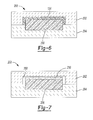
- FIG 6 is a cross section showing a detail of the present invention before firing
- FIG 7 is a cross section showing the detail of FIG 6 after firing
- FIG 8 is a cross section showing another detail of the present invention before firing
- FIG 9 is a cross section showing the detail of FIG 8 after firing
- FIG 10 is a cross section of yet another detail of the present invention.
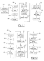
- FIG 11 is a flow diagram of a process that forms the present invention.
- FIG 12 is a flow diagram of another process that forms the present invention.
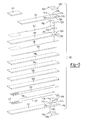
- FIG 5 is an exploded view of an exhaust sensor 100.
- exhaust sensor 100 is similar to exhaust sensor 10 of the prior art, however exhaust sensor 100 employs an expansion zone and venting feature as will be further described herein.
- the expansion zone and venting feature enable palladium to be employed instead of platinum for forming circuit features such as heaters, circuit traces and pads, sense elements, and the like.
- Exhaust sensor 100 is formed from layers of ceramics and metal inks that are fired together to form a unitary laminar structure.
- a sensor layer 102 such as zirconia, can be sandwiched between a sensor protective layer 104 and a structure of one or more support/insulating layers 106a-106d, which are collectively referred to as support/insulating layer 106.
- Sensor protective layer 104 and support/insulating layers 106 can be formed from alumina or the like.
- a sacrificial ("fugitive") material 108 such as carbon ink, is applied to support/insulating layers 106 at the interface with sensor layer 102.
- Sacrificial material 108 volatilizes during firing and leaves a void air reference channel that is in communication with one side of sensor layer 102.
- a porous protection layer or diffusion restriction layer 110 applied to sensor layer 102, allows exhaust gas to reach one side of sensor layer 102 while protecting sensor layer 102 from moisture and/or contamination with particulates.
- Exhaust sensor 100 also includes a heater 114 that heats sensor layer 102.
- the heater 114 is positioned between support/insulating layers 106 and a heater protective layer 112.
- the heater 114 is formed from palladium, and as shown, is serpentine in shape. Palladium is also employed to form pairs of pads 116a and 116b and associated conductive vias 117a, 117b and 117c. In a like manner, palladium is employed to form corresponding pairs of pads 118a and 118b associated conductive vias 119a, 119b and 119c. Pads 116a and 118a provide a power connection to heater 114 through a heater lead 120 and 122, respectively. Heater leads 120 and 122 are also formed with palladium.
- a fugitive ink 124 is printed over heater 114 and heater leads 120 and 122.
- Fugitive ink 124 may be organic in nature and may use carbon latex spheres, flour, carbon black powder, or other materials that volatilize during firing and therefore leave a void in the ceramic lamination. The volatilized ink escapes through one or more venting features that are described below. The resulting void provides space for palladium oxide to form without stressing the adjoining layers of exhaust sensor 100. It will be appreciated that while fugitive ink 124 is shown as a trace for palladium heater 114 and heater leads120 and 122, its use is not limited to those applications. Fugitive ink 124 may be employed between any of the layers in exhaust sensor 100 to provide space for palladium oxide to form without generating pressure that could separate adjacent laminated layers.
- Pads 130a-130b and 132a-132b are disposed on opposite sides of protective layer 104, while pads 132b and 132c are adjacent. As shown in FIG 5 , pads 130a-130b and 132a-132b are interconnected with vias 131a, 131b and 131c and vias 133a, 133b and 133c, respectively. Pad 132c is connected to vias 135a, 135b and 135c on sensor layer 102. Pads 132a-132c, in combination with vias 133a-133c and vias 135a-135c communicate with a lead 136. In a like manner, pads 130a and 130b, in combination with 131a-131c, communicates with a lead 134. The construction described and shown provides a connection to a signal voltage that develops across sensor layer 102.
- Exhaust sensor 200 includes a palladium circuit trace 206.
- Palladium circuit trace 206 is formed or printed with palladium ink.
- a first ceramic tape layer 202 is laminated to a second ceramic tape layer 204.
- the first ceramic layer 202 and second ceramic layer 204 is formed from alumina. It will be appreciated that other suitable materials known to one in the art may be substituted.
- Palladium circuit trace 206 is positioned on ceramic tape layer 204 and will ultimately be between first ceramic layer 202 and second ceramic layer 204.
- Fugitive ink 124 is printed over palladium circuit trace 206 prior to ceramic tape layers 202 and 204 being laminated together. Fugitive ink 124 therefore occupies space between palladium circuit trace 206 and first ceramic layer 202 when ceramic layers 202 and 204 are fired.
- Expansion space 208 provides room for palladium circuit trace 206 to form palladium oxidation 210 without cracking or delaminating first ceramic layer 202 and second ceramic layer 204.
- FIG 8 a second embodiment is shown of exhaust sensor 200 in which an orifice venting feature 212 has been added.
- Orifice venting feature 212 vents the gasses generated by fugitive ink 124 when exhaust sensor 200 is volatilized during firing.
- Venting feature 212 can simply be the open orifice prior to firing, or venting feature 212 can contain fugitive ink 124, as shown in FIG 8 , to assure that orifice venting feature 212 stays open during lamination.
- FIG 9 a cross section is shown of the exhaust sensor 200 of FIG 8 , after firing. Fugitive ink 124 has volatilized and escaped through venting feature 212, leaving behind expansion space 208 and palladium oxidation 210.
- FIG 10 is a cross section of the exhaust sensor 200 first seen in FIG 6 , with the addition of a contact pad 214.
- Contact pad 214 is printed after exhaust sensor 200 is fired by filling orifice venting feature 212 with palladium ink and forming contact pad 214 on the exterior surface of ceramic tape layer 202.
- the resulting sensor 200 has contact orifice pad 214 providing an electrical contact through venting feature 212 to palladium circuit trace 206.
- Contact pad 214 and the palladium in orifice 212 also seals orifice venting feature 212 to prevent moisture, debris, and the like from entering expansion space 208.
- Method 300 begins by forming venting features 212 with a punching process 302 through a first sheet of green ceramic that will ultimately be singulated.
- the punched sheet of green ceramic after singulation will become a plurality of first layers 202 of a plurality of exhaust sensors 200.
- a palladium circuit trace 206 is printed on a second sheet of green ceramic, such as second layer 204.
- the fugitive ink 124 is also printed over circuit trace 206 in step 304.
- the method then proceeds to step 306, where assembly occurs by registering the venting features 212 of the first sheet with its associated palladium circuit traces 206 on the second sheet and the fugitive ink 124 on the second sheet.
- first and second sheets are laminated together in step 308.
- the lamination step 308 can be performed with heat and pressure.
- the laminated sheets form first layer 202 and second layer 204, which are best shown in FIG 6 .
- Individual exhaust sensors 200 are formed in step 310 by cutting or singulating the first and second sheets of laminated first layer 202 and second layer 204. This results in a plurality of individual exhaust sensor 200 that still require further processing.
- laminated layers 202 and 204 are then fired. Firing bums out a laminating binder and sinters the ceramic layers.
- An inspection step, as identified at block 314 inspects exhaust sensor 200 for defects such as plugged venting features 212, delaminated first layer 202 and second layer 204, and the like.
- the porous protection layer or diffusion restriction layer 110 identified as step 318, is added during the printing steps 304, if desired. Porous protection layer 110 is primarily employed when exhaust sensor 200 implements an oxygen sensor.
- Contact pads 214 are applied and the filling of orifice venting features 212 are carried out in step 320.
- the method of manufacture of exhaust sensor 200 finishes at block 324 where the finished exhaust sensors 200 is tested to verify that each one is operative.
- FIG 12 depicts a second method 400 of manufacturing exhaust sensor 200.
- Second method 400 differs from method 300 in that method 400 singulates the sensors after they are fired instead of before they are fired. Depending on available equipment, this may allow second method 400 to be more efficient by printing contact pads 214, vias, or orifice venting features 212 while a plurality of exhaust sensors 200 are still together in a single laminate. Exhaust sensors 200 are then singulated after being fired.
- Method 400 begins at block 402 by punching orifice venting features 212 through a sheet of green ceramic.
- the sheet of green ceramic will, upon singulation, provide a plurality of first layers 202 for a plurality of sensors 200.
- the palladium circuit trace 206 and fugitive ink are printed on a second sheet of green ceramic.
- the second sheet will become, upon singulation, a plurality of second layers 204.
- first and second green ceramic sheets are aligned so that orifice venting features 212 are registered with associated palladium circuit traces 206.
- the aligned green sheets may also be hot pinned to maintain the registration.
- the green layers are laminated together; thereby forming a plurality of first layer 202 and second layer 204 in a single lamination.
- method 400 then proceeds to, if necessary, removing offal from the laminated first and second layers 212, as shown in step 410.
- the entirety of laminated first and second layers 202, 204, still in a single lamination are then fired, as seen in step 412.
- the firing bums out any binder that was employed and sinters the ceramic sheets.
- Method 400 then proceeds to block 414 and prints contact pads 214 and orifice venting features 212, also shown in FIG 5 as 117a-117c, 119a-119c vias 131a-131c, 133a-133c and 135a-135c.
- Method 400 then proceeds to block 416, where heat treating of contact pads 214 fixes them on the exterior surface of the laminate, thereby sealing venting features 212.
- singulation of the fired laminate into individual exhaust sensors 200 occurs after heat treating, as shown in step 418. Inspection of exhaust sensors 200 for defects such as cracking, lamination separation, and the like occurs as step 420.
- the porous protection layer or diffusion restriction layer 110 is applied to exhaust sensors 200, if needed at step 422. Porous protection layer 110 is primarily employed when exhaust sensor 200 implements an oxygen sensor.
- Method 400 then proceeds to block 424 and heat treating again is performed, this time on the completed exhaust sensors 200 prior to final testing in step 426.
Landscapes
- Chemical & Material Sciences (AREA)
- Life Sciences & Earth Sciences (AREA)
- Health & Medical Sciences (AREA)
- Physics & Mathematics (AREA)
- Chemical Kinetics & Catalysis (AREA)
- Electrochemistry (AREA)
- Molecular Biology (AREA)
- Analytical Chemistry (AREA)
- Biochemistry (AREA)
- General Health & Medical Sciences (AREA)
- General Physics & Mathematics (AREA)
- Immunology (AREA)
- Pathology (AREA)
- Measuring Oxygen Concentration In Cells (AREA)
Abstract
An exhaust sensor includes a first sheet of ceramic that is perforated with a vent orifice and, a second sheet of ceramic that is laminated to the first sheet. A palladium circuit trace is positioned between the first sheet and the second sheet of ceramic and a fugitive ink is printed on one of the sheets that is in communication with the vent orifice and the palladium. The fugitive ink volatilizes during a firing process and created a void space that is occupied by a palladium oxide that forms at temperatures around 625-900C.
Description
- The present disclosure relates to eliminating structural stress due to palladium oxide within a ceramic laminate structure.
- Planar exhaust sensor elements are manufactured using multiple layers of alumina, porous, and zirconia tapes. Metallic features are printed on the various layers using platinum conductive ink. The multiple layers of printed tapes are laminated together, and this laminated composite is fired at high temperatures to yield a fully dense multi-layer ceramic element. The metalized features can be designed either on the surface of, or embedded within, the element. For embedded features, small holes through the tape called "vias" are filled with the conductive ink in order to carry the electrical circuit through the layers of insulating tape. All of the metalized features, both surface and embedded, typically come together in a pad of metal at the surface where an electrical connection to the outside circuit is made by way of soldering, brazing, pressure contacts, etc. This pad is known as the contact pad.
- Referring now to
FIG. 1 , an exploded view is shown of anexhaust sensor 10 in accordance with the prior art just describedExhaust sensor 10 may implement a temperature sensor, a heater, a lambda sensor, an oxygen sensor, or the like.Exhaust sensor 10 is formed from layers of green ceramics and metal inks that are layered and then fired together to form a unitary laminar structure. - A
sensor layer 12 may be formed from zirconia.Sensor layer 12 may be sandwiched between a sensorprotective layer 14 and a stack of support/insulatinglayers 16a-16c, which are collectively referred to as support/insulating layers 16. Sensorprotective layer 14 and support/insulating layers 16 can be formed from alumina. Asacrificial material 20, such as carbon ink, can be applied to support/insulating layers 16 at the interface withsensor layer 12.Sacrificial material 20 volatilizes during firing and leaves a void air reference channel that is in communication with one side ofsensor layer 12. Aporous protection layer 15 allows exhaust gas to reach one side ofsensor layer 12 while protectingsensor layer 12 from moisture and/or particulates. -
Exhaust sensor 10 also includes a heater that heatssensor layer 12. Aseparator layer 18 may be formed from alumina and positioned between support/insulating layers 16 and a heaterprotective layer 22. The heater is positioned betweenseparator layer 18 and heaterprotective layer 22. The heater is formed from aplatinum heater serpentine 24. Platinum may also be employed to form pairs ofpads 26a-26b and 28a-28b. Pads 26a-26b and 28a-28b provide a power connection toheater serpentine 24 via associated heater leads 30 and 32. - Platinum may also be employed to form
pads 40a-40b andvias 42a-42c, which provide a connection to a signal voltage that is developed acrosssensor layer 12.Pads 40a-40b and 42a-42c communicate withelectrode lead 44 andelectrode lead 46, respectively. Electrode leads 44 and 46 are also formed of platinum. - The electrical features of
exhaust sensor 10, such asheater serpentine 24, heater leads 30 and 32, pads 26, 28, electrode leads 44 and 46, andpads e.g. heater serpentine 24, electrode leads 44 and 46, and the various pads, can be designed either on the surface of, or embedded within,exhaust sensor 10. For embedded metallized features, vias are punched through the green ceramic. The vias are filled with the conductive ink and fired to make electrical connections with a circuit.Exhaust sensor 10 also includes contact pads that are formed on an exterior ofexhaust sensor 10. The contact pads provide an external connection to the metallized features regardless of whether they are internal or external ofexhaust sensor 10. - Referring now to
FIGS 2 and 3 , cross sections are shown of a portion ofexhaust sensor 10.Heater lead 32 is laminated betweenseparator layer 18 and heaterprotective layer 22. Alamination region 40 indicates whereseparator layer 18 and heaterprotective layer 22 are laminated together.Pad 28b provides an attachment point for anelectrical lead 42.Electrical lead 42 can be resistance welded, brazed, soldered, or otherwise attached to via 28. Avia 44 includes a plated or inkedconductor 44 that electrically connectspad 28b andheater lead 32.FIG 3 omitspad 28b and via 44 for the sake of clarity. - As shown in
FIG 4 , there are some drawbacks to this design. Firing the green laminated ceramics releases gases from organic binders. These gases expand and can cause defects such as the delamination ofregion 40 or bubble formation in the ceramic material. Both are causes of scrap and in-service failures. These problems can be minimized by adding a venting feature, e.g. one or moreopen vias 44, to allow the gasses to escape without causing cracks and/or bubbles during firing. - However, the venting feature introduces another failure mode in service. The open venting feature can permit contaminants, such as dissolved ionic compounds in water, to enter the element under some service conditions. This weakens the ceramic materials and may cause spalling, cracking, and other failures.
- Another drawback is the high cost of the platinum metallization. Platinum is one of the few metals that have a melting/vaporization point high enough to withstand the firing temperature of the ceramic materials. It also has catalytic properties that are well suited to sensor functions. For metal features not related to those sensor functions, however, efforts have been made to replace platinum with palladium, palladium alloy, or related metals and alloys thereof, all of which are collectively referred to herein as "palladium."
- Palladium is less expensive than platinum and will stand up to the temperatures needed to co-fire the ceramic materials reasonably well. Unlike platinum, however, palladium forms an oxide. Palladium oxide reversibly forms at approximately the same temperature where oxygen sensors operate, beginning at around 625 deg C and decomposing around 850-900 deg C. There is a considerable volume increase, such as around 38%, associated with the formation of the related metal oxidation.
- The volume difference between oxidized and unoxidized palladium causes some risk when palladium is used for embedded metallized features. During firing and potentially during service, the oxygen sensor will cycle through temperatures that will cause formation and decomposition of the oxide. This oxidation/decomposition process occurs during the firing process and may also occur during operation in service if the element is not hermetically sealed. The volume change on oxidation is likely to cause cracking and/or delamination.
- The invention is related to an exhaust sensor, comprising a first sheet of ceramic that includes an orifice vent opening and a second sheet of ceramic that is laminated to the first sheet and a palladium circuit trace that is positioned between the first sheet and the second sheet of ceramic. In the sensor, a fugitive ink further occupies at least a portion of the orifice vent opening. The fugitive ink may be carbon ink. The first and second sheets of ceramic are comprised of alumina.The palladium is palladium ink. The exhaust sensor may further comprise an electrically conductive via that is formed in the orifice vent opening, a conductive pad being formed over the orifice vent opening.
- The invention is also realated to a method of making such an exhaust sensor. The method comprises the steps of perforating an orifice vent opening through a first ceramic sheet; printing a palladium circuit trace on a second ceramic sheet; printing a fugitive ink to register with the palladium circuit trace; laminating the first ceramic sheet with the second ceramic sheet such that the palladium circuit trace and fugitive ink are sandwiched between the first ceramic sheet and the second ceramic sheet and registered with the orifice vent opening; and volatilizing the fugitive ink such that it leaves a void space between the first and second sheets allowing palladium oxide to form.
- The method may further comprise printing the fugitive ink into the orifice vent opening, the fugitive ink being carbon ink.Also, the first and second ceramic sheets may comprise alumina and the palladium may be palladium ink. Further method step may be forming an electronically conductive via in the orifice vent opening and sealing the venting feature with a conductive pad in contact with the conductive via.
- The invention is also related to an exhaust sensor, comprising a first sheet of ceramic that is perforated with a plurality of vent orifices, a second sheet of ceramic that is laminated to the first sheet and a palladium circuit traces that are positioned between the first sheet and the second sheet of ceramic, a fugitive ink in communication with the vent orifices and the palladium circuit traces; and a palladium oxide disposed within a void space created by the fugitive ink volatilizing after a firing process. The fugitive ink may be carbon ink.The first and second sheets of ceramic may comprise alumina and the palladium circuit traces may comprises an electric heater element and at least one lead connected thereto where at least one conductive pad that seals at least one of the plurality of vent orifices and that is electrically connected to said at least one lead.
- The present disclosure will become more fully understood from the detailed description and the accompanying drawings, wherein:
-
FIG 1 is an exploded view of an exhaust sensor in accordance with the prior art; -
FIGS 2-4 are cross- sections of different details of exhaust sensors in accordance with the prior art; -
FIG 5 is an exploded view of an exhaust sensor in accordance with the present invention; -
FIG 6 is a cross section showing a detail of the present invention before firing; -
FIG 7 is a cross section showing the detail ofFIG 6 after firing; -
FIG 8 is a cross section showing another detail of the present invention before firing; -
FIG 9 is a cross section showing the detail ofFIG 8 after firing; -
FIG 10 is a cross section of yet another detail of the present invention; -
FIG 11 is a flow diagram of a process that forms the present invention; and -
FIG 12 is a flow diagram of another process that forms the present invention. - Referring now to
FIGS 5 through 12 , where the invention will be described with reference to specific embodiments, without limiting same,FIG 5 is an exploded view of anexhaust sensor 100. In someaspects exhaust sensor 100 is similar toexhaust sensor 10 of the prior art, howeverexhaust sensor 100 employs an expansion zone and venting feature as will be further described herein. The expansion zone and venting feature enable palladium to be employed instead of platinum for forming circuit features such as heaters, circuit traces and pads, sense elements, and the like. -
Exhaust sensor 100 is formed from layers of ceramics and metal inks that are fired together to form a unitary laminar structure. Asensor layer 102, such as zirconia, can be sandwiched between a sensorprotective layer 104 and a structure of one or more support/insulatinglayers 106a-106d, which are collectively referred to as support/insulating layer 106. Sensorprotective layer 104 and support/insulating layers 106 can be formed from alumina or the like. A sacrificial ("fugitive")material 108, such as carbon ink, is applied to support/insulating layers 106 at the interface withsensor layer 102.Sacrificial material 108 volatilizes during firing and leaves a void air reference channel that is in communication with one side ofsensor layer 102. A porous protection layer ordiffusion restriction layer 110, applied tosensor layer 102, allows exhaust gas to reach one side ofsensor layer 102 while protectingsensor layer 102 from moisture and/or contamination with particulates. -
Exhaust sensor 100 also includes aheater 114 that heatssensor layer 102. Theheater 114 is positioned between support/insulating layers 106 and a heaterprotective layer 112. Theheater 114 is formed from palladium, and as shown, is serpentine in shape. Palladium is also employed to form pairs ofpads conductive vias pads conductive vias Pads heater 114 through aheater lead - A
fugitive ink 124 is printed overheater 114 and heater leads 120 and 122.Fugitive ink 124 may be organic in nature and may use carbon latex spheres, flour, carbon black powder, or other materials that volatilize during firing and therefore leave a void in the ceramic lamination. The volatilized ink escapes through one or more venting features that are described below. The resulting void provides space for palladium oxide to form without stressing the adjoining layers ofexhaust sensor 100. It will be appreciated that whilefugitive ink 124 is shown as a trace forpalladium heater 114 and heater leads120 and 122, its use is not limited to those applications.Fugitive ink 124 may be employed between any of the layers inexhaust sensor 100 to provide space for palladium oxide to form without generating pressure that could separate adjacent laminated layers. -
Pads 130a-130b and 132a-132b are disposed on opposite sides ofprotective layer 104, whilepads FIG 5 ,pads 130a-130b and 132a-132b are interconnected with vias 131a, 131b and 131c andvias Pad 132c is connected to vias 135a, 135b and 135c onsensor layer 102.Pads 132a-132c, in combination with vias 133a-133c andvias 135a-135c communicate with alead 136. In a like manner,pads lead 134. The construction described and shown provides a connection to a signal voltage that develops acrosssensor layer 102. - Referring now to
FIG 6 , a cross-section is shown of a portion of anexhaust sensor 200.FIG 6 showsexhaust sensor 200 in a green or unfired state.Exhaust sensor 200 includes apalladium circuit trace 206.Palladium circuit trace 206 is formed or printed with palladium ink. A firstceramic tape layer 202 is laminated to a secondceramic tape layer 204. The firstceramic layer 202 and secondceramic layer 204 is formed from alumina. It will be appreciated that other suitable materials known to one in the art may be substituted.Palladium circuit trace 206 is positioned onceramic tape layer 204 and will ultimately be between firstceramic layer 202 and secondceramic layer 204.Fugitive ink 124 is printed overpalladium circuit trace 206 prior to ceramic tape layers 202 and 204 being laminated together.Fugitive ink 124 therefore occupies space betweenpalladium circuit trace 206 and firstceramic layer 202 whenceramic layers - Referring now to
FIG 7 , a cross section is shown of theexhaust sensor 200 ofFIG 6 after firing.Fugitive ink 124 has volatilized, leaving a void orexpansion space 208.Expansion space 208 provides room forpalladium circuit trace 206 to formpalladium oxidation 210 without cracking or delaminating firstceramic layer 202 and secondceramic layer 204. - Referring now to
FIG 8 , a second embodiment is shown ofexhaust sensor 200 in which anorifice venting feature 212 has been added. Orifice venting feature 212 vents the gasses generated byfugitive ink 124 whenexhaust sensor 200 is volatilized during firing. Ventingfeature 212 can simply be the open orifice prior to firing, or ventingfeature 212 can containfugitive ink 124, as shown inFIG 8 , to assure thatorifice venting feature 212 stays open during lamination. Referring now toFIG 9 , a cross section is shown of theexhaust sensor 200 ofFIG 8 , after firing.Fugitive ink 124 has volatilized and escaped through ventingfeature 212, leaving behindexpansion space 208 andpalladium oxidation 210. - The embodiment shown in
FIG 10 is a cross section of theexhaust sensor 200 first seen inFIG 6 , with the addition of acontact pad 214.Contact pad 214 is printed afterexhaust sensor 200 is fired by fillingorifice venting feature 212 with palladium ink and formingcontact pad 214 on the exterior surface ofceramic tape layer 202. The resultingsensor 200 hascontact orifice pad 214 providing an electrical contact through ventingfeature 212 topalladium circuit trace 206.Contact pad 214 and the palladium inorifice 212 also sealsorifice venting feature 212 to prevent moisture, debris, and the like from enteringexpansion space 208. - The process flow diagram of
FIG 11 depicts afirst method 300 of manufacturing theexhaust sensor 200.Method 300 begins by forming venting features 212 with apunching process 302 through a first sheet of green ceramic that will ultimately be singulated. The punched sheet of green ceramic after singulation, will become a plurality offirst layers 202 of a plurality ofexhaust sensors 200. - As shown at
step 304, apalladium circuit trace 206 is printed on a second sheet of green ceramic, such assecond layer 204. Thefugitive ink 124 is also printed overcircuit trace 206 instep 304. The method then proceeds to step 306, where assembly occurs by registering the venting features 212 of the first sheet with its associated palladium circuit traces 206 on the second sheet and thefugitive ink 124 on the second sheet. Thereafter, first and second sheets are laminated together instep 308. Thelamination step 308 can be performed with heat and pressure. The laminated sheets formfirst layer 202 andsecond layer 204, which are best shown inFIG 6 . -
Individual exhaust sensors 200 are formed instep 310 by cutting or singulating the first and second sheets of laminatedfirst layer 202 andsecond layer 204. This results in a plurality ofindividual exhaust sensor 200 that still require further processing. As identified atblock 312laminated layers block 314 inspectsexhaust sensor 200 for defects such as plugged venting features 212, delaminatedfirst layer 202 andsecond layer 204, and the like. The porous protection layer ordiffusion restriction layer 110, identified asstep 318, is added during the printing steps 304, if desired.Porous protection layer 110 is primarily employed whenexhaust sensor 200 implements an oxygen sensor. - Contact
pads 214 are applied and the filling of orifice venting features 212 are carried out in step 320.A heat treating step shown asstep 322, securescontact pads 214 into orifice venting features 212 and provides a secure connection topalladium circuit trace 206. The method of manufacture ofexhaust sensor 200 finishes atblock 324 where thefinished exhaust sensors 200 is tested to verify that each one is operative. - The process of
FIG 12 depicts asecond method 400 ofmanufacturing exhaust sensor 200.Second method 400 differs frommethod 300 in thatmethod 400 singulates the sensors after they are fired instead of before they are fired. Depending on available equipment, this may allowsecond method 400 to be more efficient byprinting contact pads 214, vias, or orifice venting features 212 while a plurality ofexhaust sensors 200 are still together in a single laminate.Exhaust sensors 200 are then singulated after being fired. -
Method 400 begins atblock 402 by punching orifice venting features 212 through a sheet of green ceramic. The sheet of green ceramic will, upon singulation, provide a plurality offirst layers 202 for a plurality ofsensors 200. Atstep 404 thepalladium circuit trace 206 and fugitive ink are printed on a second sheet of green ceramic. As with the first sheet, the second sheet will become, upon singulation, a plurality ofsecond layers 204. As identified inblock 406, first and second green ceramic sheets are aligned so that orifice venting features 212 are registered with associated palladium circuit traces 206. The aligned green sheets may also be hot pinned to maintain the registration. Thereafter, as shown inblock 408, the green layers are laminated together; thereby forming a plurality offirst layer 202 andsecond layer 204 in a single lamination. - Unlike the
method 300 described in relation toFIG 11 ,method 400 then proceeds to, if necessary, removing offal from the laminated first andsecond layers 212, as shown instep 410. The entirety of laminated first andsecond layers step 412. The firing bums out any binder that was employed and sinters the ceramic sheets.Method 400 then proceeds to block 414 andprints contact pads 214 and orifice venting features 212, also shown inFIG 5 as 117a-117c, 119a-119c vias 131a-131c, 133a-133c and 135a-135c.Method 400 then proceeds to block 416, where heat treating ofcontact pads 214 fixes them on the exterior surface of the laminate, thereby sealing venting features 212. Unlikemethod 300, singulation of the fired laminate intoindividual exhaust sensors 200 occurs after heat treating, as shown instep 418. Inspection ofexhaust sensors 200 for defects such as cracking, lamination separation, and the like occurs asstep 420. The porous protection layer ordiffusion restriction layer 110 is applied toexhaust sensors 200, if needed atstep 422.Porous protection layer 110 is primarily employed whenexhaust sensor 200 implements an oxygen sensor.Method 400 then proceeds to block 424 and heat treating again is performed, this time on the completedexhaust sensors 200 prior to final testing instep 426.
Claims (9)
- An exhaust sensor (100), comprising:a first sheet of ceramic (104) that includes at least one orifice vent opening;a second sheet of ceramic (106) that is laminated to the first sheet (104);characterized in that the sensor further comprisesa palladium circuit trace (102) that is positioned between the first sheet and the second sheet of ceramic
- The exhaust sensor (100) of claim 1, wherein a fugitive ink (108) further occupies at least a portion of the orifice vent opening.
- The exhaust sensor (100) of claim 2, wherein the fugitive ink (108) is carbon ink.
- The exhaust sensor (100) as set in any of the preceding claim, wherein the first and second sheets (104, 106) of ceramic are comprised of alumina.
- The exhaust sensor (100) as set in any of the preceding claim, wherein the palladium is palladium ink.
- The exhaust sensor (100) as set in any of the preceding claim, further comprising an electrically conductive via (117a, 117b, 117c) that is formed in the orifice vent opening.
- The exhaust sensor (100) of claim 5, further comprising a conductive pad (118a, 118b) formed over the orifice vent opening.
- A method of making an exhaust sensor (100) as set in any of the preceding claim, the method comprising the steps of:perforating an orifice vent opening through a first ceramic (104) sheet;printing a palladium circuit trace on a second ceramic sheet (106);printing a fugitive ink (108) to register with the palladium circuit trace;laminating the first ceramic sheet (104) with the second ceramic sheet (106) such that the palladium circuit trace and fugitive ink (108) are sandwiched between the first (104) ceramic sheet and the second ceramic (106) sheet and registered with the orifice vent opening; andvolatilizing the fugitive ink (108) such that it leaves a void space between the first and second sheets allowing palladium oxide to form.forming palladium oxide in the void space.
- The method of claim 8, further comprising sealing the venting feature.
Applications Claiming Priority (1)
| Application Number | Priority Date | Filing Date | Title |
|---|---|---|---|
| US12/623,095 US20110120863A1 (en) | 2009-11-20 | 2009-11-20 | Palladium ink exhaust sensor |
Publications (1)
| Publication Number | Publication Date |
|---|---|
| EP2327980A1 true EP2327980A1 (en) | 2011-06-01 |
Family
ID=43558408
Family Applications (1)
| Application Number | Title | Priority Date | Filing Date |
|---|---|---|---|
| EP10190606A Withdrawn EP2327980A1 (en) | 2009-11-20 | 2010-11-10 | Palladium ink exhaust sensor |
Country Status (2)
| Country | Link |
|---|---|
| US (1) | US20110120863A1 (en) |
| EP (1) | EP2327980A1 (en) |
Cited By (1)
| Publication number | Priority date | Publication date | Assignee | Title |
|---|---|---|---|---|
| DE102012201018A1 (en) * | 2012-01-24 | 2013-07-25 | Ifm Electronic Gmbh | Measuring device with air passage provided on the housing |
Families Citing this family (1)
| Publication number | Priority date | Publication date | Assignee | Title |
|---|---|---|---|---|
| CN102608182A (en) * | 2012-02-20 | 2012-07-25 | 曾咏平 | Oxygen sensor chip and manufacturing method thereof |
Citations (4)
| Publication number | Priority date | Publication date | Assignee | Title |
|---|---|---|---|---|
| US20030034245A1 (en) * | 2001-05-08 | 2003-02-20 | Lothar Diehl | Sensor element |
| US6723217B1 (en) * | 1999-10-20 | 2004-04-20 | Delphi Technologies, Inc. | Method and device for pumping oxygen into a gas sensor |
| US20060213772A1 (en) * | 2005-03-22 | 2006-09-28 | Jain Kailash C | Sensing element and method of making |
| EP2107368A2 (en) * | 2008-03-31 | 2009-10-07 | Ngk Insulator, Ltd. | Gas sensor, control device thereof and method of measuring NOx concentration |
Family Cites Families (1)
| Publication number | Priority date | Publication date | Assignee | Title |
|---|---|---|---|---|
| DE102004027630A1 (en) * | 2004-06-05 | 2006-01-05 | Robert Bosch Gmbh | Sensor element for determining a physical property of a measurement gas |
-
2009
- 2009-11-20 US US12/623,095 patent/US20110120863A1/en not_active Abandoned
-
2010
- 2010-11-10 EP EP10190606A patent/EP2327980A1/en not_active Withdrawn
Patent Citations (4)
| Publication number | Priority date | Publication date | Assignee | Title |
|---|---|---|---|---|
| US6723217B1 (en) * | 1999-10-20 | 2004-04-20 | Delphi Technologies, Inc. | Method and device for pumping oxygen into a gas sensor |
| US20030034245A1 (en) * | 2001-05-08 | 2003-02-20 | Lothar Diehl | Sensor element |
| US20060213772A1 (en) * | 2005-03-22 | 2006-09-28 | Jain Kailash C | Sensing element and method of making |
| EP2107368A2 (en) * | 2008-03-31 | 2009-10-07 | Ngk Insulator, Ltd. | Gas sensor, control device thereof and method of measuring NOx concentration |
Cited By (2)
| Publication number | Priority date | Publication date | Assignee | Title |
|---|---|---|---|---|
| DE102012201018A1 (en) * | 2012-01-24 | 2013-07-25 | Ifm Electronic Gmbh | Measuring device with air passage provided on the housing |
| DE102012201018B4 (en) * | 2012-01-24 | 2016-03-31 | Ifm Electronic Gmbh | Measuring instrument with air passage provided on the housing |
Also Published As
| Publication number | Publication date |
|---|---|
| US20110120863A1 (en) | 2011-05-26 |
Similar Documents
| Publication | Publication Date | Title |
|---|---|---|
| JP4936136B2 (en) | Sensor element, sensor element manufacturing method, and gas sensor | |
| US9528971B2 (en) | Particulate matter detection element and method of manufacturing same | |
| JP4623760B2 (en) | Method for manufacturing gas sensor element | |
| JP2003322632A (en) | Ceramic heater, multilayer gas sensor element and method of manufacturing the same, and gas sensor including multilayer gas sensor element | |
| JP4014623B2 (en) | Gas sensor | |
| JP4383897B2 (en) | Manufacturing method of laminated gas sensor element | |
| JP4570091B2 (en) | Laminated gas sensor element and gas sensor | |
| EP2327980A1 (en) | Palladium ink exhaust sensor | |
| JPH1196871A (en) | Resistance-temperature fuse and its manufacture | |
| JP2007132954A (en) | Ceramic sensor, multilayer gas sensor element, and gas sensor including multilayer gas sensor element | |
| CN112567235A (en) | Granular substance detection sensor element | |
| JP2006171013A (en) | Ceramic sensor, multilayer gas sensor element, and gas sensor including multilayer gas sensor element | |
| JP2003344348A (en) | Oxygen sensor element | |
| JP4480608B2 (en) | Wiring board | |
| JP2012242284A (en) | Method for manufacturing gas sensor element | |
| JP6437786B2 (en) | Sensor substrate, sensor device, and sensor substrate manufacturing method | |
| JP2007024670A (en) | Ceramic laminate and gas sensor including the same | |
| JP5051642B2 (en) | Sensor element, gas sensor, and sensor element manufacturing method | |
| JP4494283B2 (en) | Gas sensor and gas sensor manufacturing method | |
| JP2007115601A (en) | Chip type fuse element and its manufacturing method | |
| DE102015226020A1 (en) | Sensor element for detecting at least one property of a sample gas in a sample gas space and method for producing the same | |
| JP4693381B2 (en) | Wiring board and manufacturing method thereof | |
| CN112567234A (en) | Granular substance detection sensor element | |
| JP4824340B2 (en) | Method for manufacturing electrical elements and electrical elements, in particular sensor elements | |
| JP4574369B2 (en) | Wiring board and manufacturing method thereof |
Legal Events
| Date | Code | Title | Description |
|---|---|---|---|
| PUAI | Public reference made under article 153(3) epc to a published international application that has entered the european phase |
Free format text: ORIGINAL CODE: 0009012 |
|
| AK | Designated contracting states |
Kind code of ref document: A1 Designated state(s): AL AT BE BG CH CY CZ DE DK EE ES FI FR GB GR HR HU IE IS IT LI LT LU LV MC MK MT NL NO PL PT RO RS SE SI SK SM TR |
|
| AX | Request for extension of the european patent |
Extension state: BA ME |
|
| 17P | Request for examination filed |
Effective date: 20111201 |
|
| 17Q | First examination report despatched |
Effective date: 20161208 |
|
| STAA | Information on the status of an ep patent application or granted ep patent |
Free format text: STATUS: THE APPLICATION IS DEEMED TO BE WITHDRAWN |
|
| 18D | Application deemed to be withdrawn |
Effective date: 20170419 |