EP2325867A1 - High-dielectric constant capacitor - Google Patents
High-dielectric constant capacitor Download PDFInfo
- Publication number
- EP2325867A1 EP2325867A1 EP09176950A EP09176950A EP2325867A1 EP 2325867 A1 EP2325867 A1 EP 2325867A1 EP 09176950 A EP09176950 A EP 09176950A EP 09176950 A EP09176950 A EP 09176950A EP 2325867 A1 EP2325867 A1 EP 2325867A1
- Authority
- EP
- European Patent Office
- Prior art keywords
- layer
- capacitor
- teos
- dielectric
- dielectric layer
- Prior art date
- Legal status (The legal status is an assumption and is not a legal conclusion. Google has not performed a legal analysis and makes no representation as to the accuracy of the status listed.)
- Withdrawn
Links
Images

Classifications
-
- H—ELECTRICITY
- H10—SEMICONDUCTOR DEVICES; ELECTRIC SOLID-STATE DEVICES NOT OTHERWISE PROVIDED FOR
- H10D—INORGANIC ELECTRIC SEMICONDUCTOR DEVICES
- H10D1/00—Resistors, capacitors or inductors
- H10D1/60—Capacitors
- H10D1/68—Capacitors having no potential barriers
- H10D1/692—Electrodes
- H10D1/696—Electrodes comprising multiple layers, e.g. comprising a barrier layer and a metal layer
-
- H—ELECTRICITY
- H10—SEMICONDUCTOR DEVICES; ELECTRIC SOLID-STATE DEVICES NOT OTHERWISE PROVIDED FOR
- H10D—INORGANIC ELECTRIC SEMICONDUCTOR DEVICES
- H10D1/00—Resistors, capacitors or inductors
- H10D1/60—Capacitors
- H10D1/68—Capacitors having no potential barriers
- H10D1/682—Capacitors having no potential barriers having dielectrics comprising perovskite structures
- H10D1/688—Capacitors having no potential barriers having dielectrics comprising perovskite structures comprising barrier layers to prevent diffusion of hydrogen or oxygen
-
- H—ELECTRICITY
- H10—SEMICONDUCTOR DEVICES; ELECTRIC SOLID-STATE DEVICES NOT OTHERWISE PROVIDED FOR
- H10P—GENERIC PROCESSES OR APPARATUS FOR THE MANUFACTURE OR TREATMENT OF DEVICES COVERED BY CLASS H10
- H10P14/00—Formation of materials, e.g. in the shape of layers or pillars
- H10P14/40—Formation of materials, e.g. in the shape of layers or pillars of conductive or resistive materials
- H10P14/418—Formation of materials, e.g. in the shape of layers or pillars of conductive or resistive materials the conductive layers comprising transition metals
Definitions
- This invention relates to semiconductor devices, and more particularly to a high-dielectric constant capacitor.
- the space needed for an integrated capacitor becomes much smaller when compared to lower-k materials.
- BiCMOS Bipolar Complimentary Metal Oxide Semiconductor
- a method of manufacturing a capacitor comprising the steps of: forming a capacitor having a high-k dielectric layer sandwiched between top and bottom electrodes, the high-k dielectric layer having a dielectric constant greater than 20; and covering the capacitor with an encapsulation layer so as to protect the high-k dielectric layer from a subsequent annealing process.
- the encapsulation layer may protect the high-K dielectric material from the annealing process(es) typically used as a final step in BiMOS. By being protected from an annealing process, the dielectric constant of a capacitor according to the invention may be maintained at a high value.
- Embodiments therefore enable the integration of High-K capacitors with BiCMOS, BiMOS, CMOS or Bipolar junction transistors while maintaining a high dielectric constant, k, value of, for example, PZT (for example, in the range of 900-1600). In this way, the space needed for integrated capacitors is much smaller with respect to the conventional use of lower-k materials.
- Embodiments may provide a capacitance density of 20-100 nF/mm2 which is larger than resultant from conventional techniques employing dielectric lower-k material (having a dielectric constant less than 20, for example).
- a capacitor having a high-k dielectric layer sandwiched between top and bottom electrodes, the high-k dielectric layer having a dielectric constant greater than 20, the capacitor being characterised by comprising an encapsulation layer adapted to protect the high-k dielectric layer from an annealing process.
- Such a capacitor may therefore be combined with BiCMOS, BiMOS, CMOS or BJT technology whilst maintaining a high dielectric constant value of the dielectric layer.
- the high-k dielectric layer may have a dielectric constant greater than 100 and more preferably greater than 500.
- a semiconductor device comprising: a substrate; and a capacitor according to an embodiment formed on the substrate.
- Figure 1 shows a cross-section of a portion (i.e. the area of the device in which the capacitor is to be formed) of Si-containing substrate 10 after the formation/deposition of a tetra-ethyl-ortho-silicate (TEOS) layer 12 on an upper surface of the Si-containing substrate 10 at a high temperature (of about 700°C).
- TEOS tetra-ethyl-ortho-silicate
- FIG. 1 The structure shown in Figure 1 is composed of conventional materials well known to those skilled in the art and conventional BiCMOS or CMOS processing steps are used in forming the same.
- Si-containing substrate 10 includes any Si-containing semiconducting material such as Si, SiGe, Si/Si, Si/SiGe, polysilicon, silicon-on insulators (SOls) or combinations thereof such as a layer of polysilicon formed on a Si substrate.
- Preferred Si-containing substrates are Si and polysilicon substrates.
- the Si-containing substrate may include various active devices and/or isolation regions formed therein. For clarity, the active devices and/or isolation regions are not shown in FIG. 1A , but are meant to be included by reference numeral 10.
- the Si-containing substrate may of the p- or n-type depending on the type of devices being fabricated thereon.
- a plurality of tungsten (W) plugs 14 are formed in the TEOS layer 12 (covering the Si substrate including the bimos/cmos etc.) so as to contact the transistors or other functionality in the substrate 10.
- contact holes are formed in the TEOS layer 12 by plasma etching.
- an adhesion layer of typically 20 nm Ti and a barrier layer of 80 nm TiN is deposited over the entire structure.
- Ti is deposited preferably by PVD (sputtering), the TiN layer can be deposited by PVD (reactive sputtering) or MOCVD at elevated temperature ( ⁇ 350 - 400°C).
- the W plugs are formed by deposition of W by CVD primarily from WF6 and H 2 in the temperature range of 350 ⁇ 450°C, After deposition, the W film is etched back / CMP-ed back down to the surface of layer 12, leaving W plugs in the contacts.
- the W plugs are then covered by a bi-layer 16 (or stack) of SiN-TEOS or SiON-TEOS (this means Silicon nitride or siliconoxinitride, so a mixture of oxide and nitride).
- This is to create a stack with two different materials which will form a barrier, so holes in the first layer will not continue in the second layer.
- the layers are then subjected to an annealing process which is typically carried out in an N 2 and/or O 2 atmosphere in a furnace at 500-700°C.
- This anneal process is followed by a Rapid Thermal Annealing (RTA) process.
- RTA Rapid Thermal Annealing
- This procedure is followed to densify the stack/bi-layer 16 to make sure it cannot be penetrated by oxygen at the high RTA temperatures used for the PZT annealing.
- the RTA anneal before the PZT depositions is to make sure that no outgassing will occur from layer 16 during the RTA anneal after the PZT deposition. This encapsulation ensures that the W plugs will survive a subsequent PZT annealing procedure.
- one or more capacitors 18 are formed over at least a portion of the bi-layer 16.
- the capacitors 18 are formed by sandwiching a first high-k PZT dielectric layer 20 between top 22 and bottom 24 electrode layers, wherein the bottom electrode layer 24 is separated from the bi-layer 16 by a second high-k dielectric layer 26.
- the second high-k dielectric layer 26 TiO x -Ti or TiO x -PZT or TiO x is used, this layer does not have to be high-k but it may be favourable to use PZT because it can act as an extra H 2 protection for the real dielectric).
- high-k denotes a dielectric that has a dielectric constant of greater than 20, preferably greater than 50, more preferably greater than 100 and even more preferably greater than 500. It is noted that all the dielectric constants reported herein are relative to a vacuum having a dielectric constant of 1.
- high-k dielectrics may be employed in the present invention including, but not limited to: binary metal oxides such as TiO 2 Ta 2 O 5 A1 2 O 3 , Y 2 O 3 , ZrO 2 , HfO 2 , Gd 2 O 3 , and La 2 O 3 ; silicates, aluminates and oxynitrides of said binary metal oxides; and perovskite-type oxides. Combinations and/or multilayers of such high-k dielectrics may also be employed.
- the perovskite-type oxides may be in the crystalline or amorphous phase.
- perovskite-oxides that may be employed in the present invention as the high-k dielectric material include, but are not limited to: a titanate system material, i.e., barium titanate, strontium titanate, barium strontium titanate (BST), lead titanate, lead zirconate titanate (PZT), lead lanthanum zirconate titanate, barium zirconium titanate and barium lanthanum titanate; a niobate or tantalate system material such as lead magnesium niobate, lithium niobate, lithium tantalate, potassium niobate, strontium aluminum tantalate and potassium tantalum niobate; a tungsten-bronze system material such as barium strontium niobate, lead barium niobate, and barium titanium niobate; or a Bi-layered perovskite system material such as strontium bismuth tantalate, and bismuth
- PZT or BST for layer 20.
- doped versions of PZT and BST can be used.
- the layers of the capacitors 18 may be formed utilizing any conventional deposition process, including, but not limited to: low-pressure chemical vapour deposition (LPCVD), atomic layer chemical vapour deposition (ALCVD), rapid thermal chemical vapour deposition (RTCVD), plasma-assisted CVD, physical vapour deposition, sputtering, plating, evaporation, chemical solution deposition and other like deposition processes.
- LPCVD low-pressure chemical vapour deposition
- ACVD atomic layer chemical vapour deposition
- RTCVD rapid thermal chemical vapour deposition
- plasma-assisted CVD plasma-assisted CVD
- physical vapour deposition sputtering
- plating evaporation
- chemical solution deposition chemical solution deposition and other like deposition processes.
- the physical thickness of the high-k dielectric material employed in the present invention may vary depending on the dielectric constant and the deposition process used in forming the same. Typically, however, the high-k dielectric has a physical thickness of from about 50 to about 1000 nm, with a thickness of from about 100 to about 400 nm being preferred.
- the high-K capacitors After making the high-K capacitors a contact to the W plugs can be provided followed by a final H 2 -N 2 annealing process. However, the high-K capacitors have to be protected against the H 2 containing atmosphere of the annealing process. For this purpose, the high-K capacitors are encapsulated in a buffer or encapsulation layer 28 as shown in Figure 5 .
- the encapsulation layer covers the area of the device so as to cover the top/exposed layer of the bi-layer and top electrode layer 22 (and exposed portions) of the capacitors 18.
- This encapsulation layer can be, for example, PZT-AlO x (meaning that the exact stoichiometry of the AlO x is not that important) or TEOS-SiN(-TEOS) (or alternating layers of siliconoxides and nitrides), or PZT-TEOS-SiN-TEOS.
- a plurality of aluminium (Al) plugs 30 are formed in the buffer layer 28 and bi-layer 16 so as to extend through the buffer layer 28 and bi-layer 16 and contact the W plugs 14.
- contact holes are formed in the buffer layer 28 and bi-layer 16 by plasma etching.
- a layer of typically 500 nm ⁇ 1000 nm Al (alloy) is deposited preferably by PVD (sputtering).
- this layer is patterned using lithography and plasma etching.
- An activation annealing process is then carried out in an H 2 -N 2 atmosphere in a furnace at 400-450°C (this is the final back-end anneal to activate the W-Al contacts to the underlying BiMos/cmos).
- the encapsulation/buffer ensures that the W plugs will survive the annealing procedure so that the dielectric constant (900-1600) can be maintained.
- Al contacts 32 to the capacitor(s) are provided as shown in Figure 7 .
- embodiments enable the integration of a high-K capacitor with BiCMOS, BiMOS, CMOS or Bipolar junction transistors while maintaining a high dielectric constant value of a dielectric layer employed for the capacitor.
Landscapes
- Semiconductor Integrated Circuits (AREA)
Abstract
A method of manufacturing a capacitor (18) is presented. The method comprises forming a capacitor having a high-k dielectric layer (20) sandwiched between top (22) and bottom (24) electrodes, the high-k dielectric layer (20) having a dielectric constant greater than 20. The capacitor (18) is then covered with an encapsulation layer (28) so as to protect the high-k dielectric layer (20) from a subsequent annealing process
Description
- This invention relates to semiconductor devices, and more particularly to a high-dielectric constant capacitor.
- In the case of capacitors, the main focus is on the development of high capacitance/area devices with low series resistance of the top and bottom electrodes for high frequency responses. High capacitance/area devices require the use of dielectric materials that are thin (of the order of about 200 A or less). The use of conventional, thin low-k dielectrics (having a dielectric constant, k, of about 20 or below) in today's devices is undesirable since such materials lead to leaky devices.
- With the use of high-k dielectrics (having a dielectric constant, k, of greater than 20, and typically in the range of k=900-1600), the space needed for an integrated capacitor becomes much smaller when compared to lower-k materials. Thus, the integration of High-K (HK) capacitors with Bipolar Complimentary Metal Oxide Semiconductor (BiCMOS) technology provides a way to introduce high-density capacitors within High-K technology.
- The problem with combining these technologies is the fact that high-K capacitors do not survive the (400-450°C) forming gas (N2-H2) annealing step which is normally used as a final step in BiMOS (and related technologies). Also, tungsten (W) plugs that are typically needed to contact the transistors in BiMOS do not survive the high temperature anneal in an oxygen ambient used in High-K technology (700-800°C).
- Accordingly, it is desirable to develop a way to combine High-K technologies with BiMOS (and related technologies) which addresses the aforementioned integration difficulties.
- According to the invention, there is provided a method of manufacturing a capacitor comprising the steps of: forming a capacitor having a high-k dielectric layer sandwiched between top and bottom electrodes, the high-k dielectric layer having a dielectric constant greater than 20; and covering the capacitor with an encapsulation layer so as to protect the high-k dielectric layer from a subsequent annealing process.
- The encapsulation layer may protect the high-K dielectric material from the annealing process(es) typically used as a final step in BiMOS. By being protected from an annealing process, the dielectric constant of a capacitor according to the invention may be maintained at a high value.
- Embodiments therefore enable the integration of High-K capacitors with BiCMOS, BiMOS, CMOS or Bipolar junction transistors while maintaining a high dielectric constant, k, value of, for example, PZT (for example, in the range of 900-1600). In this way, the space needed for integrated capacitors is much smaller with respect to the conventional use of lower-k materials.
- Embodiments may provide a capacitance density of 20-100 nF/mm2 which is larger than resultant from conventional techniques employing dielectric lower-k material (having a dielectric constant less than 20, for example).
- According to another aspect of the invention, there is provided a capacitor having a high-k dielectric layer sandwiched between top and bottom electrodes, the high-k dielectric layer having a dielectric constant greater than 20, the capacitor being characterised by comprising an encapsulation layer adapted to protect the high-k dielectric layer from an annealing process. Such a capacitor may therefore be combined with BiCMOS, BiMOS, CMOS or BJT technology whilst maintaining a high dielectric constant value of the dielectric layer.
- The high-k dielectric layer may have a dielectric constant greater than 100 and more preferably greater than 500.
- According to yet another aspect, there is provided a semiconductor device comprising: a substrate; and a capacitor according to an embodiment formed on the substrate.
- Examples of the invention will now be described with reference to the accompanying drawings, in which:
-
Figures 1-7 shows are cross-sectional views of a semiconductor device through various processing steps of the present invention. - The drawings are not to scale, and some dimensions may have been exaggerated (for example the thickness dimension) to make the drawings show the different components more clearly. It is also noted that the drawings only show a portion of a device. The bipolar device region and the region containing the device transistors are not shown for simplicity. However, as one skilled in the art is aware, the bipolar devices and the device transistors may be formed in the areas that abut the capacitor area depicted in the drawings.
- Reference is made to
Figures 1-7 which illustrate the formation of a capacitor structure according to an embodiment of the invention. -
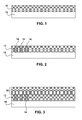
Figure 1 shows a cross-section of a portion (i.e. the area of the device in which the capacitor is to be formed) of Si-containingsubstrate 10 after the formation/deposition of a tetra-ethyl-ortho-silicate (TEOS)layer 12 on an upper surface of the Si-containingsubstrate 10 at a high temperature (of about 700°C). - The structure shown in
Figure 1 is composed of conventional materials well known to those skilled in the art and conventional BiCMOS or CMOS processing steps are used in forming the same. - For example, Si-containing
substrate 10 includes any Si-containing semiconducting material such as Si, SiGe, Si/Si, Si/SiGe, polysilicon, silicon-on insulators (SOls) or combinations thereof such as a layer of polysilicon formed on a Si substrate. Preferred Si-containing substrates are Si and polysilicon substrates. The Si-containing substrate may include various active devices and/or isolation regions formed therein. For clarity, the active devices and/or isolation regions are not shown inFIG. 1A , but are meant to be included byreference numeral 10. The Si-containing substrate may of the p- or n-type depending on the type of devices being fabricated thereon. - Next, as shown in
Figure 2 , a plurality of tungsten (W)plugs 14 are formed in the TEOS layer 12 (covering the Si substrate including the bimos/cmos etc.) so as to contact the transistors or other functionality in thesubstrate 10. In this process, contact holes are formed in theTEOS layer 12 by plasma etching. Next, after an in-situ cleaning step, an adhesion layer of typically 20 nm Ti and a barrier layer of 80 nm TiN is deposited over the entire structure. Ti is deposited preferably by PVD (sputtering), the TiN layer can be deposited by PVD (reactive sputtering) or MOCVD at elevated temperature (∼350 - 400°C). The W plugs are formed by deposition of W by CVD primarily from WF6 and H2 in the temperature range of 350 ― 450°C, After deposition, the W film is etched back / CMP-ed back down to the surface oflayer 12, leaving W plugs in the contacts. - Referring to
Figure 3 , the W plugs are then covered by a bi-layer 16 (or stack) of SiN-TEOS or SiON-TEOS (this means Silicon nitride or siliconoxinitride, so a mixture of oxide and nitride). This is to create a stack with two different materials which will form a barrier, so holes in the first layer will not continue in the second layer. - The layers are then subjected to an annealing process which is typically carried out in an N2 and/or O2 atmosphere in a furnace at 500-700°C. This anneal process is followed by a Rapid Thermal Annealing (RTA) process. This procedure is followed to densify the stack/
bi-layer 16 to make sure it cannot be penetrated by oxygen at the high RTA temperatures used for the PZT annealing. The RTA anneal before the PZT depositions is to make sure that no outgassing will occur fromlayer 16 during the RTA anneal after the PZT deposition. This encapsulation ensures that the W plugs will survive a subsequent PZT annealing procedure. - Next, and as shown in
FIG. 4 , one ormore capacitors 18 are formed over at least a portion of thebi-layer 16. Specifically, thecapacitors 18 are formed by sandwiching a first high-k PZT dielectric layer 20 betweentop 22 andbottom 24 electrode layers, wherein thebottom electrode layer 24 is separated from thebi-layer 16 by a second high-kdielectric layer 26. Here, for the second high-kdielectric layer 26, TiOx-Ti or TiOx-PZT or TiOx is used, this layer does not have to be high-k but it may be favourable to use PZT because it can act as an extra H2 protection for the real dielectric). - The term "high-k" as used herein denotes a dielectric that has a dielectric constant of greater than 20, preferably greater than 50, more preferably greater than 100 and even more preferably greater than 500. It is noted that all the dielectric constants reported herein are relative to a vacuum having a dielectric constant of 1.
- A wide variety of high-k dielectrics may be employed in the present invention including, but not limited to: binary metal oxides such as TiO2 Ta2O5 A12O3, Y2O3, ZrO2, HfO2, Gd2O3, and La2O3; silicates, aluminates and oxynitrides of said binary metal oxides; and perovskite-type oxides. Combinations and/or multilayers of such high-k dielectrics may also be employed. The perovskite-type oxides may be in the crystalline or amorphous phase.
- Examples of perovskite-oxides that may be employed in the present invention as the high-k dielectric material include, but are not limited to: a titanate system material, i.e., barium titanate, strontium titanate, barium strontium titanate (BST), lead titanate, lead zirconate titanate (PZT), lead lanthanum zirconate titanate, barium zirconium titanate and barium lanthanum titanate; a niobate or tantalate system material such as lead magnesium niobate, lithium niobate, lithium tantalate, potassium niobate, strontium aluminum tantalate and potassium tantalum niobate; a tungsten-bronze system material such as barium strontium niobate, lead barium niobate, and barium titanium niobate; or a Bi-layered perovskite system material such as strontium bismuth tantalate, and bismuth titanate.
- Of the various high-k dielectrics mentioned above, preference is given to PZT or BST for layer 20. Also doped versions of PZT and BST can be used.
- The layers of the
capacitors 18 may be formed utilizing any conventional deposition process, including, but not limited to: low-pressure chemical vapour deposition (LPCVD), atomic layer chemical vapour deposition (ALCVD), rapid thermal chemical vapour deposition (RTCVD), plasma-assisted CVD, physical vapour deposition, sputtering, plating, evaporation, chemical solution deposition and other like deposition processes. - The physical thickness of the high-k dielectric material employed in the present invention may vary depending on the dielectric constant and the deposition process used in forming the same. Typically, however, the high-k dielectric has a physical thickness of from about 50 to about 1000 nm, with a thickness of from about 100 to about 400 nm being preferred.
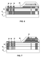
- After making the high-K capacitors a contact to the W plugs can be provided followed by a final H2-N2 annealing process. However, the high-K capacitors have to be protected against the H2 containing atmosphere of the annealing process. For this purpose, the high-K capacitors are encapsulated in a buffer or
encapsulation layer 28 as shown inFigure 5 . - The encapsulation layer covers the area of the device so as to cover the top/exposed layer of the bi-layer and top electrode layer 22 (and exposed portions) of the
capacitors 18. This encapsulation layer can be, for example, PZT-AlOx (meaning that the exact stoichiometry of the AlOx is not that important) or TEOS-SiN(-TEOS) (or alternating layers of siliconoxides and nitrides), or PZT-TEOS-SiN-TEOS. By employing the buffer or encapsulation layer, the breakdown voltage of the capacitors and the dielectric constant (900-1600) can be maintained even after a subsequent annealing process. - Next, as shown in
Figure 6 , a plurality of aluminium (Al) plugs 30 are formed in thebuffer layer 28 andbi-layer 16 so as to extend through thebuffer layer 28 andbi-layer 16 and contact the W plugs 14. In this process contact holes are formed in thebuffer layer 28 andbi-layer 16 by plasma etching. Next, after an in situ cleaning step, a layer of typically 500 nm ― 1000 nm Al (alloy) is deposited preferably by PVD (sputtering). Next, this layer is patterned using lithography and plasma etching. An activation annealing process is then carried out in an H2-N2 atmosphere in a furnace at 400-450°C (this is the final back-end anneal to activate the W-Al contacts to the underlying BiMos/cmos). - As mentioned above, the encapsulation/buffer ensures that the W plugs will survive the annealing procedure so that the dielectric constant (900-1600) can be maintained.
- Finally, after the annealing process,
Al contacts 32 to the capacitor(s) are provided as shown inFigure 7 . - It will be appreciated that embodiments enable the integration of a high-K capacitor with BiCMOS, BiMOS, CMOS or Bipolar junction transistors while maintaining a high dielectric constant value of a dielectric layer employed for the capacitor.
- Other variations to the disclosed embodiments can be understood and effected by those skilled in the art in practicing the claimed invention, from a study of the drawings, the disclosure, and the appended claims. In the claims, the word "comprising" does not exclude other elements or steps, and the indefinite article "a" or "an" does not exclude a plurality. Any reference signs in the claims should not be construed as limiting the scope.
Claims (14)
- A method of manufacturing a capacitor comprising the steps of:forming a capacitor having a high-k dielectric layer (20) sandwiched between top (22) and bottom (24) electrodes, the high-k dielectric layer (20) having a dielectric constant greater than 20; andcovering the capacitor (18) with an encapsulation layer (28) so as to protect the high-k dielectric layer (20) from a subsequent annealing process.
- The method of claim 1, wherein the encapsulation layer (28) comprises a binary metal oxide or a perovskite oxide.
- The method of claim 1, wherein the encapsulation layer (28) is formed from PZT-AlOx, TEOS-SiN or PZT-TEOS-SiN-TEOS.
- The method of claim 1, wherein the high-k dielectric layer (28) has a dielectric constant greater than 500.
- The method of claim 1, wherein the bottom electrode (24) is formed on a further high-k dielectric layer (26).
- The method of claim 5, wherein the further high-k dielectric layer (26) is formed from TiOx-PZT.
- A method of manufacturing a semiconductor device comprising the steps of:providing a substrate (10);forming a TEOS layer (12) on the substrate (10);forming a first plug (14) in the TEOS layer (12) so as to contact the substrate (10);covering the TEOS layer (12) and the first plug (14) with a buffer layer (16) so as to protect the first plug (14) from a subsequent annealing process;subjecting the buffer layer (16) to an annealing process;manufacturing a capacitor on the buffer layer (16) according to claim 1;forming a second plug (30) in the encapsulation layer (28) so as to contact the first plug (14) formed in the TEOS layer;subjecting the encapsulation layer (28) to an activation annealing process; andforming a third plug (32) in the encapsulation layer (28) so as to contact an electrode (22) of the capacitor.
- A capacitor (18) having a high-k dielectric layer (20) sandwiched between top (22) and bottom (24) electrodes, the high-k dielectric layer (20) having a dielectric constant greater than 20, the capacitor (18) being characterised by comprising an encapsulation layer (28) adapted to protect the high-k dielectric layer (20) from an annealing process.
- The capacitor of claim 8, wherein the encapsulation layer (28) comprises a binary metal oxide or a perovskite oxide.
- The capacitor of claim 8, wherein the encapsulation layer (28) is formed from PZT-AlOx, TEOS-SiN or PZT-TEOS-SiN-TEOS.
- The capacitor of claim 8, wherein the high-k dielectric layer (28) has a dielectric constant greater than 500.
- A semiconductor device comprising:a substrate (10); anda capacitor according to claim 8 formed on the substrate.
- The semiconductor device of claim 12, wherein the bottom electrode (24) of the capacitor (18) is separated from the substrate (10) by at least one of: a TEOS layer; and a further high-k dielectric layer (26).
- The semiconductor device of claim 12, further comprising a first plug for contacting the substrate and second plug for contacting an electrode of the capacitor (18).
Priority Applications (1)
| Application Number | Priority Date | Filing Date | Title |
|---|---|---|---|
| EP09176950A EP2325867A1 (en) | 2009-11-24 | 2009-11-24 | High-dielectric constant capacitor |
Applications Claiming Priority (1)
| Application Number | Priority Date | Filing Date | Title |
|---|---|---|---|
| EP09176950A EP2325867A1 (en) | 2009-11-24 | 2009-11-24 | High-dielectric constant capacitor |
Publications (1)
| Publication Number | Publication Date |
|---|---|
| EP2325867A1 true EP2325867A1 (en) | 2011-05-25 |
Family
ID=42040522
Family Applications (1)
| Application Number | Title | Priority Date | Filing Date |
|---|---|---|---|
| EP09176950A Withdrawn EP2325867A1 (en) | 2009-11-24 | 2009-11-24 | High-dielectric constant capacitor |
Country Status (1)
| Country | Link |
|---|---|
| EP (1) | EP2325867A1 (en) |
Citations (4)
| Publication number | Priority date | Publication date | Assignee | Title |
|---|---|---|---|---|
| US6211542B1 (en) * | 1996-08-20 | 2001-04-03 | Ramtron International Corporation | Completely encapsulated top electrode of a ferroelectric capacitor using a lead-enhanced escapsulation layer |
| WO2001024237A1 (en) * | 1999-09-28 | 2001-04-05 | Symetrix Corporation | Integrated circuits with barrier layers and methods of fabricating same |
| US20020175361A1 (en) * | 2001-05-22 | 2002-11-28 | Glen Fox | Charge pump or other charge storage capacitor including pzt layer for combined use as encapsulation layer and dielectric layer of ferroelectric capacitor and a method for manufacturing the same |
| WO2008028660A2 (en) * | 2006-09-06 | 2008-03-13 | Nxp B.V. | Device with pb-based high-k dielectric thin-film capacitor comprising pb-donating layers |
-
2009
- 2009-11-24 EP EP09176950A patent/EP2325867A1/en not_active Withdrawn
Patent Citations (4)
| Publication number | Priority date | Publication date | Assignee | Title |
|---|---|---|---|---|
| US6211542B1 (en) * | 1996-08-20 | 2001-04-03 | Ramtron International Corporation | Completely encapsulated top electrode of a ferroelectric capacitor using a lead-enhanced escapsulation layer |
| WO2001024237A1 (en) * | 1999-09-28 | 2001-04-05 | Symetrix Corporation | Integrated circuits with barrier layers and methods of fabricating same |
| US20020175361A1 (en) * | 2001-05-22 | 2002-11-28 | Glen Fox | Charge pump or other charge storage capacitor including pzt layer for combined use as encapsulation layer and dielectric layer of ferroelectric capacitor and a method for manufacturing the same |
| WO2008028660A2 (en) * | 2006-09-06 | 2008-03-13 | Nxp B.V. | Device with pb-based high-k dielectric thin-film capacitor comprising pb-donating layers |
Non-Patent Citations (1)
| Title |
|---|
| IN SEON PARK ET AL: "Ultra-thin EBL (encapsulated barrier layer) for ferroelectric capacitor", ELECTRON DEVICES MEETING, 1997. TECHNICAL DIGEST., INTERNATIONAL WASHINGTON, DC, USA 7-10 DEC. 1997, NEW YORK, NY, USA,IEEE, US, 7 December 1997 (1997-12-07), pages 617 - 620, XP010265582, ISBN: 978-0-7803-4100-5 * |
Similar Documents
| Publication | Publication Date | Title |
|---|---|---|
| US6255122B1 (en) | Amorphous dielectric capacitors on silicon | |
| US7868421B2 (en) | Analog capacitor | |
| CN102473681B (en) | Methods of forming capacitors | |
| US7623338B2 (en) | Multiple metal-insulator-metal capacitors and method of fabricating the same | |
| US6326258B1 (en) | Method of manufacturing semiconductor device having thin film capacitor | |
| US8570706B2 (en) | Tantalum-based electrode stack | |
| KR20030013626A (en) | Method of forming stacked capacitor | |
| JP3643091B2 (en) | Semiconductor memory device and manufacturing method thereof | |
| JP2000260959A (en) | Iridium conductive electrode / barrier structure and method of forming the same | |
| JP2003068993A (en) | Semiconductor device and method of manufacturing the same | |
| US7407897B2 (en) | Capacitor of analog semiconductor device having multi-layer dielectric film and method of manufacturing the same | |
| US7323419B2 (en) | Method of fabricating semiconductor device | |
| US6339007B1 (en) | Capacitor stack structure and method of fabricating description | |
| US20020105048A1 (en) | Dielectric element including oxide dielectric film and method of manufacturing the same | |
| US20090256259A1 (en) | Semiconductor device and method for manufacturing the same | |
| US8940601B2 (en) | Manufacturing method of semiconductor device | |
| US6468874B1 (en) | Method of manufacturing a capacitor in a semiconductor device | |
| EP2325867A1 (en) | High-dielectric constant capacitor | |
| US7244979B2 (en) | Semiconductor memory device and method for manufacturing the same | |
| US20060151845A1 (en) | Method to control interfacial properties for capacitors using a metal flash layer | |
| US7170736B2 (en) | Capacitor having low resistance electrode including a thin silicon layer | |
| US20030058678A1 (en) | Ferroelectric memory device and method of fabricating the same | |
| JP4067079B2 (en) | Semiconductor device and manufacturing method thereof | |
| US7528429B2 (en) | Ferroelectric capacitor and semiconductor device | |
| JP2008192914A (en) | Semiconductor device and manufacturing method thereof |
Legal Events
| Date | Code | Title | Description |
|---|---|---|---|
| PUAI | Public reference made under article 153(3) epc to a published international application that has entered the european phase |
Free format text: ORIGINAL CODE: 0009012 |
|
| AK | Designated contracting states |
Kind code of ref document: A1 Designated state(s): AT BE BG CH CY CZ DE DK EE ES FI FR GB GR HR HU IE IS IT LI LT LU LV MC MK MT NL NO PL PT RO SE SI SK SM TR |
|
| AX | Request for extension of the european patent |
Extension state: AL BA RS |
|
| STAA | Information on the status of an ep patent application or granted ep patent |
Free format text: STATUS: THE APPLICATION IS DEEMED TO BE WITHDRAWN |
|
| 18D | Application deemed to be withdrawn |
Effective date: 20111126 |