EP2323012A2 - Energy saving circuit for a peripheral, peripheral, distribution device and work method - Google Patents
Energy saving circuit for a peripheral, peripheral, distribution device and work method Download PDFInfo
- Publication number
- EP2323012A2 EP2323012A2 EP10182261A EP10182261A EP2323012A2 EP 2323012 A2 EP2323012 A2 EP 2323012A2 EP 10182261 A EP10182261 A EP 10182261A EP 10182261 A EP10182261 A EP 10182261A EP 2323012 A2 EP2323012 A2 EP 2323012A2
- Authority
- EP
- European Patent Office
- Prior art keywords
- peripheral device
- circuit
- data bus
- data
- energy
- Prior art date
- Legal status (The legal status is an assumption and is not a legal conclusion. Google has not performed a legal analysis and makes no representation as to the accuracy of the status listed.)
- Withdrawn
Links
Images


Classifications
-
- G—PHYSICS
- G06—COMPUTING; CALCULATING OR COUNTING
- G06F—ELECTRIC DIGITAL DATA PROCESSING
- G06F1/00—Details not covered by groups G06F3/00 - G06F13/00 and G06F21/00
- G06F1/26—Power supply means, e.g. regulation thereof
- G06F1/32—Means for saving power
- G06F1/3203—Power management, i.e. event-based initiation of a power-saving mode
- G06F1/3234—Power saving characterised by the action undertaken
- G06F1/325—Power saving in peripheral device
- G06F1/3253—Power saving in bus
-
- Y—GENERAL TAGGING OF NEW TECHNOLOGICAL DEVELOPMENTS; GENERAL TAGGING OF CROSS-SECTIONAL TECHNOLOGIES SPANNING OVER SEVERAL SECTIONS OF THE IPC; TECHNICAL SUBJECTS COVERED BY FORMER USPC CROSS-REFERENCE ART COLLECTIONS [XRACs] AND DIGESTS
- Y02—TECHNOLOGIES OR APPLICATIONS FOR MITIGATION OR ADAPTATION AGAINST CLIMATE CHANGE
- Y02D—CLIMATE CHANGE MITIGATION TECHNOLOGIES IN INFORMATION AND COMMUNICATION TECHNOLOGIES [ICT], I.E. INFORMATION AND COMMUNICATION TECHNOLOGIES AIMING AT THE REDUCTION OF THEIR OWN ENERGY USE
- Y02D10/00—Energy efficient computing, e.g. low power processors, power management or thermal management
-
- Y—GENERAL TAGGING OF NEW TECHNOLOGICAL DEVELOPMENTS; GENERAL TAGGING OF CROSS-SECTIONAL TECHNOLOGIES SPANNING OVER SEVERAL SECTIONS OF THE IPC; TECHNICAL SUBJECTS COVERED BY FORMER USPC CROSS-REFERENCE ART COLLECTIONS [XRACs] AND DIGESTS
- Y02—TECHNOLOGIES OR APPLICATIONS FOR MITIGATION OR ADAPTATION AGAINST CLIMATE CHANGE
- Y02D—CLIMATE CHANGE MITIGATION TECHNOLOGIES IN INFORMATION AND COMMUNICATION TECHNOLOGIES [ICT], I.E. INFORMATION AND COMMUNICATION TECHNOLOGIES AIMING AT THE REDUCTION OF THEIR OWN ENERGY USE
- Y02D30/00—Reducing energy consumption in communication networks
- Y02D30/50—Reducing energy consumption in communication networks in wire-line communication networks, e.g. low power modes or reduced link rate
Definitions
- the present invention relates to a power saving circuit for a peripheral device for connection to a data bus of a host system.
- it relates to a peripheral device and a switching device for a data bus with such energy saving circuit and a working method for such energy saving circuit.
- Peripheral devices for connection to a data bus of a host system are widely known. Examples of such peripheral devices are external storage drives, printers or scanners connected to a host adapter of a computer system. But in other areas of technology, peripheral devices are connected via data buses. Examples include consumer electronics or communications electronics.
- peripheral devices have their own power supply for supplying the peripheral device with an operating voltage. This has the consequence that the peripheral devices are usually supplied with energy even when switching off a host system. Both the peripheral device itself and the power supply unit used to supply the peripheral device cause a power loss. This power loss usually consists to a large extent of losses of switching converters of the power supply.
- an electronic power supply unit which has a control unit, which voltage-transforming elements of a power supply separates depending on a power requirement of a connected electronic device from a primary-side AC voltage.
- the object of the present invention is to describe a power saving circuit for a peripheral device for connection to a data bus of a host system, which reduces a power consumption of the peripheral device in a standby state without disturbing a communication of the data bus.
- peripheral device a switching device and a working method are to be described, which are suitable for use with the energy saving circuit.
- a power-saving circuit for a peripheral device for connection to a data bus of a host system comprising a monitoring circuit for monitoring communication via the data bus, a latch circuit for holding a connection state of the peripheral device and at least one switching element for interrupting a supply voltage for the peripheral device.
- the power save circuit further includes a control circuit configured to detect a start of an idle state of the data bus by the monitor circuit and to hold the connection state of the peripheral device by activating the hold voltage upon detection of a start of the idle state and to supply the power supply to the peripheral device Opening the at least one switching element to interrupt.
- the power saving circuit By holding a connection state of the peripheral device by a latch circuit, even during an idle state of the data bus, the appearance of bus disconnection for the host system can be inhibited. In doing so, during the idle state of the data bus, the power saving circuit performs the function of maintaining a connection state, so that the peripheral device can be disconnected from a power supply voltage without disturbing the communication via the data bus.
- control circuit is further configured to detect an end of an idle state of the data bus by the monitoring circuit.
- the control circuit upon detection of an end of the idle state, restores supply of the peripheral device supply voltage by closing the at least one switching element and enables the connection state of the peripheral device by disabling the latch circuit.
- the additional detection of an end of the idle state and the reconnection of the peripheral device with the supply voltage and the deactivation of the holding circuit For example, the operating state that existed before the idling state started can be restored.
- the host system may transmit data via the data bus at least at a first and a second speed.
- the connection state of the peripheral device determines whether the peripheral device is set for data transmission at the first or second speed.
- the data bus includes at least a first data line and a second data line, and the latch circuit is configured to maintain the first data line at a predetermined voltage level when the peripheral device is set for data transmission at the first speed and to maintain the second data line at a predetermined voltage level when the peripheral device is set up for data transmission at the second speed.
- Such an embodiment of the energy-saving circuit makes it possible to successfully connect the peripheral device to the data bus again after a separation from a supply voltage and to exchange data with the host system at a previously determined speed, without requiring a renewed initialization of the peripheral device or of the host system.
- the energy saving circuit according to the invention is particularly suitable for installation in a peripheral device according to claim 12 or a switching device for a data bus according to claim 13.
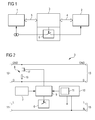
- FIG. 1 shows a first arrangement comprising a host system 1, a peripheral device 2 and an energy saving circuit 3 connected between the host system 1 and the peripheral device 2.
- the host system 1 is, for example, a desktop PC.
- the peripheral device 2 in the exemplary embodiment is a printer which is connected to a host adapter of the host system 1 by means of a serial data bus.
- the peripheral device 2 is connected to the energy-saving circuit 3 with a first data cable 4.
- the energy saving circuit 3 is connected to the host system 1 with a second data cable 5.
- the power saving circuit 3 is electrically connected between the host system 1 and the peripheral device 2, and can monitor communication via the data bus.
- the energy saving circuit 3 comprises a first switching element 6 in the form of a relay.
- the first switching element 6 is between a power supply network that provides an AC line voltage, and the peripheral device 2. By opening the first switching element 6, the power-saving circuit 3 can completely disconnect the peripheral device 2 from the power supply network.
- FIG. 2 shows a schematic representation of the energy saving circuit 3.
- the energy saving circuit 3 comprises in addition to the first switching element 6 for separating a phase line L, a monitoring circuit 7 and a holding circuit 8.
- the energy saving circuit 3 comprises a control circuit 9, the monitoring circuit 7, the holding circuit 8 and first switching element 6 controls.
- the energy saving circuit 6 further includes a switching converter 10 and an energy storage 11th
- a data line D and a reference line GND of the data bus are looped through the energy-saving circuit 3.
- signals received at a first terminal 12 of the deactivated power-saving circuit 3 are also available at the second terminal 13 to which the peripheral device 2 is connected.
- a primary-side mains connection 14 for connecting the energy-saving circuit 3 to a power supply network is connected via the first switching element 6 to a switching output 15 of the energy-saving circuit 3. At the switching output 15, a power supply of the peripheral device 2 is connected.
- the monitoring circuit 7 is set up to monitor a signaling on the data line D of the data bus.
- the monitoring circuit 7 detects whether data is exchanged between the peripheral device 2 and the host system 1 or whether the bus system is in an idle state, in which either no data or a predetermined control signal indicative of the idle state is transmitted. If the presence of such an idling state detected by the monitoring circuit 7, it generates a corresponding control signal for the control circuit. 9
- the control circuit 9 detects the control signal supplied from the monitoring circuit 7 and causes disconnection of the peripheral device 2 from the bus system without disturbing the host system 1.
- the data line D is connected via a so-called pull-down resistor 16 and a transistor 17 to the reference line GND.
- the data line D is pulled via the pull-down resistor 16 to a ground potential of the reference line GND.
- the pull-down resistor 16 replaces a termination of the data bus by the peripheral device 2.
- the control circuit 9 therefore draws the data line D to the potential of the reference line GND upon detection of an idle state of the bus system via the monitoring circuit 7, and then opens the first switching element 6, so that the peripheral device 2 is disconnected from the power supply network and during the idle state of the bus system receives no additional energy from the power grid.
- the control circuit 9 activates the peripheral device 2 again in a manner that is transparent to the host system 1.
- the control circuit 9 for this purpose first activates the peripheral device 2 by closing the first switching element 6.
- the transistor 17 is further driven by the control circuit 9. If the peripheral device 2 is again completely ready for operation, the control signal for the transistor 17 is interrupted by the control circuit 9 and thus the data line D is disconnected from the reference line GND. Subsequently, an undisturbed communication takes place between the peripheral device 2 and the host system 1 via the data line D.
- the data bus according to FIG. 2 In the exemplary embodiment, there is no line for providing a supply voltage.
- the energy saving circuit 3 comprises the additional switching converter 10, which generates a DC voltage for supplying the components of the energy saving circuit 3 from a mains side AC voltage.
- the switching converter 10 is arranged behind the first switching element 6 in the embodiment. Thus, the switching converter 10 is disconnected in the idle state of the bus system from the power supply network.
- the energy storage 11 for example, a rechargeable battery or a high-capacity capacitor stores sufficient electric power to the control circuit 9 for a predetermined standby period, for example, one hour after the idle state is activated, with an operating power supply.
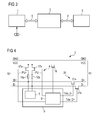
- FIG. 3 shows an alternative arrangement comprising a host system 1, a peripheral device 2 and a power saving circuit 3.
- the host system 1 and the peripheral device 2 in turn connected via a serial data bus, here a USB bus with an integrated power supply line.
- the peripheral device 2 is supplied with an operating voltage via the USB bus.
- the arrangement according to FIG. 3 Therefore, only the host system 1 is connected to a power supply network.
- FIG. 4 shows a schematic representation of the structure of the power-saving circuit 3 for the USB bus system according to FIG. 3
- Both a first terminal 12 and a second terminal 13 of the energy saving circuit 3 each comprise two differential data lines D + and D- and two supply lines VCC and GND. These lines are looped through the energy-saving circuit 3, wherein the supply line VCC can be separated by means of a second switching element 18.
- the second switching element 18 is a field effect transistor.
- the energy-saving circuit after FIG. 4 has a monitoring circuit 7, a control circuit 9 and a holding circuit 8.
- the monitoring circuit 7 and the control circuit 9 are integrated in a common microcontroller 19.
- the holding circuit 8 comprises a first transistor 17a and a second transistor 17b for connecting the first data line D + via a first resistor 16a to the supply line VCC and the second data line D- via a second resistor 16b to the supply line VCC.
- the power-saving circuit 3 has an optional interrupting circuit 20.
- the interruption circuit 20 comprises two third switching elements 21a and 21b, through which the data lines D + and D- between the first terminal 12 and the second terminal 13 can be separated. As a result, leakage currents in the direction of a peripheral device 2 connected to the second connection 13 can be prevented.
- the interruption circuit 20 By separating the data lines D + and D- by the interruption circuit 20, data transmission between the peripheral device 2 and the host system 1 can also be inhibited even if the peripheral device 2 is supplied with an operating voltage via an external power supply unit. In this way, in particular a waking up of the host system 1 by the peripheral device 2 can be avoided.
- the microcontroller 19 is supplied via the power supply lines VCC and GND with an operating voltage. This is for the sake of clarity in the FIG. 4 but not shown. According to the USB specification, a so-called full power or low power peripheral device in the so-called suspend state may draw 500 pA or 2.5 mA current via the supply line. This is sufficient for the operation of the microcontroller 19 according to the embodiment.
- the monitoring circuit 7 monitors the data bus comprising the data lines D + and D-. In addition to monitoring a signaling of the beginning or the end of an idle state of the data bus, the monitoring circuit 7 also monitors an operating mode of a peripheral device 2 connected to the second connection 13.
- an idle state is initiated on the USB bus in the normal operating state of the host system 1, for example, the ACPI state S0 of the operating system, if the USB peripheral device 2 is not used.
- the peripheral device 2 is placed in the so-called Suspend state. This can also be achieved by a global or selective suspend command of the host system 1.
- a power-saving state such as one of the ACPI conditions S3, S4 or S5
- the host system 1 in the embodiment also sent a suspend command.
- USB peripheral device 2 Once the host system 1 signals an idle state to the peripheral device 2, it must initiate a suspend state within 3 ms. Each USB peripheral device 2 must respond to USB commands from host system 1 immediately, whether it is a global suspend or selective suspend command, or an idle state signaling. Optimized drivers and software running on host system 1 can improve the use of these power-saving modes.
- USB peripheral device 2 is a low-speed (LS), full-speed (FS) or high-speed (HS) device, so-called keep-alive signals usually become available sent via the USB bus.
- LS low-speed
- FS full-speed
- HS high-speed
- keep-alive signals usually become available sent via the USB bus.
- SOF Start of Frame
- USB peripherals 2 must go into suspend state within 3 ms on detection of the constant idle state of the so-called upstream port, so the host system 1 or a higher-level USB hub. After a further 10 ms, peripheral device 2 is only allowed to record the standard-defined suspend current from the USB bus. In the suspend state, the peripheral device 2 must continue to provide a voltage via the data line D + in the high or full speed mode and in the low speed mode via the data line D-, so that the idle state can be maintained. For this purpose, the supply line VCC is connected via a so-called pull-up resistor to the corresponding data line D + or D-. This, together with the upstream host system 1 or USB hub, ensures correct compliance with the USB specification.
- High-speed peripherals 2 There are additional requirements for suspending high-speed peripherals 2 because a reset and an idle state for high-speed peripherals 2 can not be clearly distinguished.
- High-speed peripherals must therefore switch from high-speed mode to full-speed mode after 3 ms idle, or at the latest after 3.125 ms.
- a receiving circuit is separated from the differential data line D + and D- and the data line D + is connected via a pull-up resistor of the peripheral device 2 to the supply line VCC.
- Peripheral device 2 must monitor lines D + and D- no sooner than 100 ⁇ s and not later than 875 ⁇ s after switching to the full-speed mode.
- the peripheral device 2 remains in the suspend state. If so an SEO Start of Packet, so a transition in idle in the so-called K State is detected, then it is a reset signal to reset the peripheral device 2, which is then triggered.
- USB devices indicate whether they are operating in high or full speed mode or low speed mode by pulling up data lines D + and D-, respectively.
- the current bus state is detected and simulated by the connection of the corresponding pull-up resistor 16a or 16b of the latch 8.
- the control circuit 9 activates upon detection of an idle state via the monitoring circuit 7, either the first transistor 17a for signaling a device with a full-speed mode or the second transistor 17b for signaling a device with a low-speed mode. This prevents the host system 1 from detecting a bus separation when the peripheral device 2 is switched off and a reconnection to the bus system when it is switched on again, which would otherwise be signaled to the operating system of the host system 1.
- the energy-saving circuit 3 responds and then controls the second switching element 18 such that the power supply of the peripheral device 2 is interrupted.
- the supply line VCC bus-powered peripherals 2 can be separated from the supply voltage without a connected to the first terminal 12 host system 1 notices the deactivation of the peripheral device 2.
- the data lines D + and D- are separated via the interruption circuit 20.
- a peripheral device 2 For a peripheral device 2 to return from the suspend state, it must be woken up via a so-called resume sequence.
- a peripheral device 2 starts the resume as soon as another bus state (English: non-idle state) than the idle state is applied to the upstream port. So-called wakeup-enabled USB peripheral devices 2 can also wake the host system 1 from the suspend state.
- the host system 1 is always entitled to send the resume sequence (TDRSMDN) which is on the bus for at least 20ms. Depending on the device speed, the host system must terminate the resume sequence with two different end sequences. For full and low-speed peripherals 2, a low-speed EOP (end-of-packet: two low-speed bit periods of single-ended SEO followed by a J state) is signaled. If the peripheral device was in the high-speed mode when it was suspended, resume signaling must be initiated with a high-speed idle sequence. The control of the host system 1 must additionally ensure a 10 ms long resume recovery time (TRSMRCY) before the awakened peripherals 2 may be accessed.
- TRSMRCY resume recovery time
- the host system 1 initiates the resume state by means of a level change on the data lines D + and D-, this is detected by the monitoring circuit 7 and evaluated by the control circuit 8. Then, the supply voltage is switched through the second switching element 18 again to the second terminal 13, and the pull-up resistors 16a and 16b are separated from the data lines D + and D-.
- the optional interruption circuit 20 then becomes optional deactivated to restore a connection of the data lines between the first terminal 12 and the second terminal 13. In the exemplary embodiment, this takes place synchronously with the deactivation of the transistors 17a and 17b, so that an uninterrupted takeover by a device-internal pull-up resistor takes place and thus no device separation is triggered. Thereafter, the peripheral device 2 returns from the suspend state to the normal operating state in consideration of the time requirements of the USB specification.
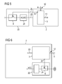
- FIG. 5 shows a peripheral device 2 with an external power supply 22.
- the peripheral device 2 according to FIG. 5 includes a power-saving circuit 3.
- the power-saving circuit 3 is similar to that in the FIG. 2 constructed energy saving circuit 3 and provides a control signal via a control signal output 23 to the peripheral device 2 ready.
- the control signal from the control output 23 is used to interrupt a power supply to the external power supply 22.
- the power supply 22 includes a first switching element 6 for disconnecting a converter circuit 24 from a power supply network.
- the power supply 22 and the peripheral device 2 are connected to each other via a supply line 25 for transmitting a DC voltage.
- they are connected to one another by an additional control line 26 for transmitting the control signal from the control output 23 to the first switching element 6 of the power supply 22.
- control signal of the control output 23 can also be modulated onto the supply line 25 for transmitting the supply voltage.
- a high-frequency AC voltage signal can be modulated onto a DC supply voltage.
- FIG. 6 shows a peripheral device 2 with an internal power supply 22.
- the operation of the peripheral device 2 according to FIG. 6 largely corresponds to that of the peripheral device 2 in FIG. 5 , Since the power supply 22 according to FIG. 6 However, integrated into the peripheral device 2, can be dispensed with an external connection between the peripheral device 2 and the power supply 22, which in particular facilitates the control of the first switching element 6 of the power supply 22.
- FIG. 7 shows a switching device 27 for connecting two peripheral devices 2a and 2b to a common host system 1.
- the first peripheral device 2a is remotely powered via a data bus from the switching device 27 with an operating power.
- the first peripheral device 2a with a bus line 28a, which includes both data lines and supply lines, connected to the switching device 27.
- the second peripheral device 2b is supplied with an operating power by an external power supply 22.
- the second peripheral device 2b is connected to the switching device 27 via a second bus line 28b.
- the power supply 22 is connected to a switching output 15b of the switching device 27.
- it is a switchable socket, which is associated with a second terminal 13b for the second peripheral device 2b.
- the switching device 27 comprises a power saving circuit 3, which is constructed similar to those described above. Specifically, the power saving circuit 3 monitors the communication between the host system 1 and the peripherals 2a and 2b. When no data is transmitted from the host system 1 to the peripheral devices 2a or 2b, the first peripheral device 2a and the second peripheral device 2b, respectively, become one Power supply disconnected. In the case of the supplied via the switching device 27 peripheral device 2a only one supply line of the bus line 28a is interrupted for this purpose, as for example with reference to the FIG. 4 has been described. In the case of the second peripheral device 2b, the switching output 15b of the switching device 27 configured as a socket is deactivated so that the power pack 22 is disconnected from the power supply network.
- a switching converter 10 of the switching device 27 can also be disconnected from the power supply network.
- the power-saving circuit 3 is supplied with an operating power either from the host system 1 or from an internal energy store of the switching device 27, as described above.
- FIG. 8 shows an exemplary signaling of an idle state via a USB bus.
- a host system 1 in the exemplary embodiment a personal computer, is in a normal operating state, for example the so-called ACPI operating state S0.
- a data transmission takes place via differential data lines D + and D- of a USB bus.
- data packets with a frame duration of one millisecond are sent either via the USB low-speed standard or according to the USB full-speed standard via the data lines D + and D-.
- the host system 1 If no further data is to be exchanged between the host system 1 and the peripheral device 2, the host system 1 signals an idle state at a time T1. In this state, neither data nor control signals are exchanged over the data lines D + and D-. In particular, not even so-called start-off-frame (SOF) packets are sent over the data bus in this bus operating state.
- SOF start-off-frame
- the power-saving circuit 3 After a predetermined idle time Tidle of at least three milliseconds, the power-saving circuit 3 detects that there is no activity on the data bus. Then, depending on a predetermined transmission mode, it pulls either the positive data line D + or the negative data line D- to a predetermined voltage level. Thereafter, a corresponding control signal for interrupting a primary mains voltage and / or a secondary DC voltage of a supply line of the data bus is generated. In this way, it is ensured that the peripheral device 2 does not receive any further energy in the idle state of the bus system.
- the peripheral device 2 is reconnected to the data bus.
- the energy saving circuit 3 first detects a resumption of the signaling via the data bus. For example, an explicit resume signal is provided by the host system 1. Alternatively, it is also possible to detect data packets with a preceding SOF signal.
- the control circuit 9 activates first the first switching element 6 and / or the second switching element 18 for providing a mains voltage to a power supply 22 or a supply voltage via a supply line of the data bus.
- the peripheral device 2 starts running and is in an operational state within a predefined period of time Tstart. Thereafter, the latch circuit 8 is de-activated by canceling the corresponding control signals for pulling up the positive data line D + and the negative data line D, respectively.
- the data is processed by the peripheral device 2 and communication with the host system 1 is continued.
- the host system 1 does not generate a corresponding interrupt which is normally evaluated by an operating system of the host system 1 when other peripheral devices 2 are connected.
- FIG. 9 shows a flowchart of a working procedure for a power saving circuit 3.
- a first step A1 it is monitored in a loop whether the bus system is in an idle state. If the bus system is not in an idle state, a timer for determining an idle time is reset in a step A2. Steps A1 and A2 are repeated until an idle state is detected.
- step A3 If the bus system is in an idling state, a check is made in a subsequent step A3 as to whether a predetermined period for applying the idling state has been reached. For example, it checks to see if a USB bus is in an idle state for more than three milliseconds. If this is not yet the case, the method continues in step A1.
- a connection state of a peripheral device 2 is detected in a step A4. For example, it is detected whether a peripheral device 2 communicates with a host system 1 in a so-called low-speed or in a full-speed mode. Separate monitoring for the use of a high-speed mode is not required because peripheral devices that communicate in the high-speed mode first change back to the full-speed mode before transitioning to an idle state.
- a holding circuit 8 is then activated first.
- a resistor 16 is connected across a transistor 17 between a data line and a supply line to pull the data line to a predetermined voltage level.
- a switching element 6 and / or a second switching element 18 is opened in order to prevent a power supply of the peripheral device 2.
- the peripheral device 2 therefore does not receive any further electrical energy from a power supply network.
- the energy saving circuit 3 is suitable for integration into individual devices, as a separate additional circuit arranged between a host system 1 and a peripheral device 2 and for arrangement in switching components such as a USB hub or switch.
- the solution described is suitable in addition to the USB bus for other bus systems, the detection of an idle state allow.
- it is suitable for bus systems that include a supply line, which allows a supply of energy-saving circuit 3 via the bus system, even when peripheral devices are switched off.
- bus systems include eSATA, Firewire (IEEE 1394), external PCI Express and Power over Ethernet (PoE, IEEE 802.3af).
- An energy saving can be improved by further optimizing a host-side control of the bus system.
- it can be specified in an operating system from which period of inactivity of a single device either the entire bus system or individual peripheral devices 2 connected to the bus system are to be put into a suspend state.
- the host system 1 is configured so that when switched to a power-saving state, for example, an ACPI S3, S4 or S5 state, the data bus is basically placed in an idle state, so that connected to the data bus peripherals 2 together with the host system 1 in go over a power saving state.
- the idle state signaling is not tied to a particular protocol layer.
- a supply line of a data bus is deactivated in an energy-saving state of the host system 1. If the monitoring circuit 7 recognizes a deactivation of a supply voltage on one of the supply lines, this can likewise be used to detect an idle state and for the subsequent deactivation of a peripheral device 2.
Abstract
Description
Die vorliegende Erfindung betrifft eine Energiesparschaltung für ein Peripheriegerät zum Anschluss an einen Datenbus eines Hostsystems. Darüber hinaus betrifft sie ein Peripheriegerät und ein Vermittlungsgerät für einen Datenbus mit einer derartigen Energiesparschaltung sowie ein Arbeitsverfahren für eine derartige Energiesparschaltung.The present invention relates to a power saving circuit for a peripheral device for connection to a data bus of a host system. In addition, it relates to a peripheral device and a switching device for a data bus with such energy saving circuit and a working method for such energy saving circuit.
Peripheriegeräte zum Anschluss an einen Datenbus eines Hostsystems sind vielfach bekannt. Beispiele solcher Peripheriegeräte sind externe Speicherlaufwerke, Drucker oder Scanner, die mit einem Hostadapter eines Computersystems verbunden sind. Aber auch in anderen Bereichen der Technik werden Peripheriegeräte über Datenbusse angeschlossen. Beispiele hierfür sind Geräte der Unterhaltungselektronik oder der Kommunikationselektronik.Peripheral devices for connection to a data bus of a host system are widely known. Examples of such peripheral devices are external storage drives, printers or scanners connected to a host adapter of a computer system. But in other areas of technology, peripheral devices are connected via data buses. Examples include consumer electronics or communications electronics.
Viele Peripheriegeräte weisen ein eigenes Netzteil zur Versorgung des Peripheriegerätes mit einer Betriebsspannung auf. Dies hat zur Folge, dass die Peripheriegeräte in der Regel auch beim Abschalten eines Hostsystems weiter mit Energie versorgt werden. Dabei verursacht sowohl das Peripheriegerät selbst als auch das zur Versorgung des Peripheriegerätes genutzte Netzteil eine Verlustleistung. Diese Verlustleistung besteht in der Regel zu einem großen Teil aus Verlusten von Schaltwandlern des Netzteils.Many peripheral devices have their own power supply for supplying the peripheral device with an operating voltage. This has the consequence that the peripheral devices are usually supplied with energy even when switching off a host system. Both the peripheral device itself and the power supply unit used to supply the peripheral device cause a power loss. This power loss usually consists to a large extent of losses of switching converters of the power supply.
Aus der
Die Lösung gemäß dem Stand der Technik weist jedoch den Nachteil auf, dass unter Umständen eine unbeabsichtigte Deaktivierung des Peripheriegerätes stattfindet, wenn dessen Leistungsaufnahme absinkt, ohne dass eine Kommunikation mit einem Hostsystem unterbrochen wurde. Dies führt unter Umständen zu einer Fehlermeldung auf Seiten eines mit dem Peripheriegerät verbundenen Hostsystems, wenn das Peripheriegerät wider Erwarten nicht mehr über einen Datenbus ansprechbar ist. Des Weiteren kann es hierbei auch zu Datenverlusten kommen, insbesondere beim Ansprechen von Massenspeichermedien.The solution according to the prior art, however, has the disadvantage that inadvertent deactivation of the peripheral device takes place when its power consumption drops, without interrupting communication with a host system. This may result in an error message on the part of a host system connected to the peripheral device if, contrary to expectations, the peripheral device is no longer accessible via a data bus. Furthermore, this can also lead to data loss, especially when addressing mass storage media.
Aufgabe der vorliegenden Erfindung ist es, eine Energiesparschaltung für ein Peripheriegerät zum Anschluss an einen Datenbus eines Hostsystems zu beschreiben, das eine Leistungsaufnahme des Peripheriegerätes in einem Bereitschaftszustand vermindert ohne eine Kommunikation des Datenbusses zu stören.The object of the present invention is to describe a power saving circuit for a peripheral device for connection to a data bus of a host system, which reduces a power consumption of the peripheral device in a standby state without disturbing a communication of the data bus.
Darüber hinaus sollen ein Peripheriegerät, ein Vermittlungsgerät und ein Arbeitsverfahren beschrieben werden, die zur Verwendung mit der Energiesparschaltung geeignet sind.In addition, a peripheral device, a switching device and a working method are to be described, which are suitable for use with the energy saving circuit.
Die oben genannten Aufgabe wird durch eine Energiesparschaltung für ein Peripheriegerät zum Anschluss an einen Datenbus eines Hostsystems gelöst, wobei die Energiesparschaltung eine Überwachungsschaltung zur Überwachung einer Kommunikation über den Datenbus, eine Halteschaltung zum Halten eines Verbindungszustands des Peripheriegerätes und wenigstens ein Schaltelement zum Unterbrechen einer Versorgungsspannung für das Peripheriegerät aufweist. Die Energiesparschaltung umfasst des Weiteren eine Steuerschaltung, die dazu eingerichtet ist, einen Beginn eines Leerlaufzustands des Datenbusses durch die Überwachungsschaltung zu erkennen und bei Erkennung eines Beginns des Leerlaufzustands den Verbindungszustand des Peripheriegerätes durch Aktivieren der Haltespannung zu halten sowie eine Zufuhr der Versorgungsspannung für das Peripheriegerät durch Öffnen des wenigstens einen Schaltelementes zu unterbrechen.The above object is achieved by a power-saving circuit for a peripheral device for connection to a data bus of a host system, the power-saving circuit comprising a monitoring circuit for monitoring communication via the data bus, a latch circuit for holding a connection state of the peripheral device and at least one switching element for interrupting a supply voltage for the peripheral device. The power save circuit further includes a control circuit configured to detect a start of an idle state of the data bus by the monitor circuit and to hold the connection state of the peripheral device by activating the hold voltage upon detection of a start of the idle state and to supply the power supply to the peripheral device Opening the at least one switching element to interrupt.
Durch Halten eines Verbindungszustands des Peripheriegerätes durch eine Halteschaltung kann auch während eines Leerlaufzustandes des Datenbusses der Anschein einer Bustrennung für das Hostsystem unterbunden werden. Dabei übernimmt die Energiesparschaltung während des Leerlaufzustands des Datenbusses die Funktion, einen Verbindungszustand aufrecht zu erhalten, so dass das Peripheriegerät ohne Störung der Kommunikation über den Datenbus von einer Versorgungsspannungszufuhr getrennt werden kann.By holding a connection state of the peripheral device by a latch circuit, even during an idle state of the data bus, the appearance of bus disconnection for the host system can be inhibited. In doing so, during the idle state of the data bus, the power saving circuit performs the function of maintaining a connection state, so that the peripheral device can be disconnected from a power supply voltage without disturbing the communication via the data bus.
Gemäß einer vorteilhaften Ausgestaltung ist die Steuerschaltung des Weiteren dazu eingerichtet, ein Ende eines Leerlaufzustands des Datenbusses durch die Überwachungsschaltung zu erkennen. Die Steuerschaltung stellt bei Erkennung eines Endes des Leerlaufzustandes die Zufuhr der Versorgungsspannung für das Peripheriegerät durch Schließen des wenigstens einen Schaltelementes wieder her und gibt den Verbindungszustand des Peripheriegerätes durch Deaktivieren der Halteschaltung frei. Durch die zusätzliche Erkennung eines Endes des Leerlaufzustandes und das Wiederverbinden des Peripheriegerätes mit der Versorgungsspannung sowie der Deaktivierung der Halteschaltung kann der Betriebszustand, der vor Beginn des Leerlaufzustandes vorgelegen hat, wiederhergestellt werden.According to an advantageous embodiment, the control circuit is further configured to detect an end of an idle state of the data bus by the monitoring circuit. The control circuit, upon detection of an end of the idle state, restores supply of the peripheral device supply voltage by closing the at least one switching element and enables the connection state of the peripheral device by disabling the latch circuit. The additional detection of an end of the idle state and the reconnection of the peripheral device with the supply voltage and the deactivation of the holding circuit For example, the operating state that existed before the idling state started can be restored.
Gemäß weiteren vorteilhaften Ausgestaltungen kann das Hostsystem wenigstens mit einer ersten und einer zweiten Geschwindigkeit Daten über den Datenbus übertragen. Der Verbindungszustand des Peripheriegerätes legt fest, ob das Peripheriegerät für eine Datenübertragung mit der ersten oder der zweiten Geschwindigkeit eingerichtet ist. Der Datenbus umfasst wenigstens eine erste Datenleitung und eine zweite Datenleitung und die Halteschaltung ist dazu eingerichtet, die erste Datenleitung auf einen vorbestimmten Spannungspegel zu halten, wenn das Peripheriegerät für eine Datenübertragung mit der ersten Geschwindigkeit eingerichtet ist und die zweite Datenleitung auf einen vorbestimmten Spannungspegel zu halten, wenn das Peripheriegerät für eine Datenübertragung mit der zweiten Geschwindigkeit eingerichtet ist. Eine derartige Ausgestaltung der Energiesparschaltung ermöglicht es, das Peripheriegerät nach einer Trennung von einer Versorgungsspannung wieder erfolgreich mit dem Datenbus zu verbinden und mit einer zuvor ermittelten Geschwindigkeit Daten mit dem Hostsystem auszutauschen, ohne dass es einer erneuten Initialisierung des Peripheriegerätes oder des Hostsystems bedarf.According to further advantageous embodiments, the host system may transmit data via the data bus at least at a first and a second speed. The connection state of the peripheral device determines whether the peripheral device is set for data transmission at the first or second speed. The data bus includes at least a first data line and a second data line, and the latch circuit is configured to maintain the first data line at a predetermined voltage level when the peripheral device is set for data transmission at the first speed and to maintain the second data line at a predetermined voltage level when the peripheral device is set up for data transmission at the second speed. Such an embodiment of the energy-saving circuit makes it possible to successfully connect the peripheral device to the data bus again after a separation from a supply voltage and to exchange data with the host system at a previously determined speed, without requiring a renewed initialization of the peripheral device or of the host system.
Die erfindungsgemäße Energiesparschaltung eignet sich insbesondere zum Einbau in ein Peripheriegerät gemäß Patentanspruch 12 oder ein Vermittlungsgerät für einen Datenbus gemäß Patentanspruch 13.The energy saving circuit according to the invention is particularly suitable for installation in a peripheral device according to
Die oben genannte Aufgabe wird ebenso durch ein Arbeitsverfahren für eine zwischen einem Hostsystem und einem Peripheriegerät angeordnete Energiesparschaltung mit den folgenden Schritten gelöst:
- Ermitteln eines Verbindungszustands des Peripheriegerätes;
- Erkennen eines Leerlaufzustands des Datenbusses durch Überwachen des Datenbusses;
- Halten des Verbindungszustands des Peripheriegerätes durch Bereitstellen eines Steuersignals für das Hostsystem; und
- Auftrennen einer dem Peripheriegerät zugeordneten Stromversorgungsleitung durch Öffnen wenigstens eines Schaltelementes.
- Determining a connection state of the peripheral device;
- Detecting an idle state of the data bus by monitoring the data bus;
- Maintaining the connection state of the peripheral device by providing a control signal to the host system; and
- Separating a power supply line assigned to the peripheral device by opening at least one switching element.
Weitere vorteilhafte Ausgestaltungen der Erfindung sind in den Unteransprüchen sowie der nachfolgenden, ausführlichen Beschreibung offenbart.Further advantageous embodiments of the invention are disclosed in the subclaims and the following detailed description.
Die Erfindung wird anhand unterschiedlicher Ausführungsbeispiele unter Bezugnahme auf Figuren näher erläutert. In den Figuren zeigen:
-
Figur 1 -
Figur 2Figur 1 -
Figur 3 -
Figur 4Figur 3 -
Figur 5 -
Figur 6 -
Figur 7 -
Figur 8 -
Figur 9
-
FIG. 1 a first arrangement comprising a peripheral device, a power saving circuit and a host system, -
FIG. 2 a schematic representation of a first energy saving circuit for the arrangement according toFIG. 1 . -
FIG. 3 a second arrangement comprising a peripheral device, a power saving circuit and a host system, -
FIG. 4 a schematic representation of a second energy saving circuit for the second arrangement according toFIG. 3 . -
FIG. 5 a first peripheral device with an external power supply for power, -
FIG. 6 a second peripheral device with an integrated power supply unit, -
FIG. 7 a schematic representation of a switching device with an integrated energy saving circuit, -
FIG. 8 a schematic representation of bus signals, and -
FIG. 9 a flowchart of a method for a power saving circuit.
Im Ausführungsbeispiel handelt es sich bei dem Hostsystem 1 beispielsweise um einen Desktop-PC. Bei dem Peripheriegerät 2 handelt es sich im Ausführungsbeispiel um einen Drucker, der mittels eines seriellen Datenbusses mit einem Hostadapter des Hostsystems 1 verbunden ist. Im Ausführungsbeispiel ist das Peripheriegerät 2 mit einem ersten Datenkabel 4 mit der Energiesparschaltung 3 verbunden. Die Energiesparschaltung 3 ist mit einem zweiten Datenkabel 5 mit dem Hostsystem 1 verbunden. Somit ist die Energiesparschaltung 3 elektrisch zwischen das Hostsystem 1 und das Peripheriegerät 2 geschaltet und kann eine Kommunikation über den Datenbus überwachen.In the exemplary embodiment, the
Die Energiesparschaltung 3 umfasst ein erstes Schaltelement 6 in Form eines Relais. Das erste Schaltelement 6 ist zwischen einem Stromversorgungsnetz, das eine Netzwechselspannung bereitstellt, und dem Peripheriegerät 2 angeordnet. Durch Öffnen des ersten Schaltelementes 6 kann die Energiesparschaltung 3 das Peripheriegerät 2 vollständig von dem Stromversorgungsnetz trennen.The
Wie aus der
Die Überwachungsschaltung 7 ist dazu eingerichtet, eine Signalisierung auf der Datenleitung D des Datenbusses zu überwachen. Die Überwachungsschaltung 7 erkennt, ob Daten zwischen dem Peripheriegerät 2 und dem Hostsystem 1 ausgetauscht werden oder ob das Bussystem sich in einem Leerlaufzustand befindet, in dem entweder gar keine Daten oder ein vorbestimmtes Steuersignal, das den Leerlaufzustand anzeigt, übertragen werden. Wird das Vorliegen eines solchen Leerlaufzustandes durch die Überwachungsschaltung 7 erkannt, erzeugt sie ein entsprechendes Steuersignal für die Steuerschaltung 9.The
Die Steuerschaltung 9 erkennt das von der Überwachungsschaltung 7 gelieferte Steuersignal und veranlasst eine Trennung des Peripheriegerätes 2 von dem Bussystem ohne das Hostsystem 1 zu stören. Hierzu wird im Ausführungsbeispiel zunächst die Datenleitung D über einen so genannten Pull-Down-Widerstand 16 und einen Transistor 17 mit der Referenzleitung GND verbunden. Beispielsweise wird die Datenleitung D über den Pull-Down-Widerstand 16 auf ein Massepotenzial der Referenzleitung GND gezogen.The
Im Ausführungsbeispiel ersetzt der Pull-Down-Widerstand 16 eine Terminierung des Datenbusses durch das Peripheriegerät 2. Die Steuerschaltung 9 zieht bei Erkennen eines Leerlaufzustands des Bussystems über die Überwachungsschaltung 7 daher zunächst die Datenleitung D auf das Potenzial der Referenzleitung GND und öffnet dann das erste Schaltelement 6, so dass das Peripheriegerät 2 von dem Stromversorgungsnetz getrennt wird und während des Leerlaufzustandes des Bussystems keine weitere Energie aus dem Stromversorgungsnetz aufnimmt.In the exemplary embodiment, the pull-down resistor 16 replaces a termination of the data bus by the
Am Ende des Leerlaufzustandes aktiviert die Steuerschaltung 9 das Peripheriegerät 2 erneut in einer Weise, die für das Hostsystem 1 transparent ist. Im Ausführungsbeispiel aktiviert die Steuerschaltung 9 hierfür zunächst das Peripheriegerät 2 durch Schließen des ersten Schaltelementes 6. Während einer vorbestimmten Vorlaufzeit, die das Peripheriegerät 2 benötigt, um wieder in einen normalen Betriebszustand zu gelangen, wird der Transistor 17 weiterhin durch die Steuerschaltung 9 angesteuert. Ist das Peripheriegerät 2 wieder vollständig betriebsbereit, wird das Steuersignal für den Transistor 17 durch die Steuerschaltung 9 unterbrochen und somit die Datenleitung D von der Referenzleitung GND getrennt. Anschließend findet wieder eine ungestörte Kommunikation zwischen dem Peripheriegerät 2 und dem Hostsystem 1 über die Datenleitung D statt.At the end of the idle state, the
Der Datenbus gemäß
Auch die Energiesparschaltung nach
Die Energiesparschaltung 3 weist eine optionale Unterbrechungsschaltung 20 auf. Die Unterbrechungsschaltung 20 umfasst zwei dritte Schaltelemente 21a und 21b, durch die die Datenleitungen D+ und D- zwischen dem ersten Anschluss 12 und dem zweiten Anschluss 13 aufgetrennt werden können. Dadurch können Leckströme in Richtung eines an den zweiten Anschluss 13 angeschlossenen Peripheriegeräts 2 verhindert werden. Durch ein Auftrennen der Datenleitungen D+ und D- durch die Unterbrechungsschaltung 20 kann außerdem eine Datenübertragung zwischen dem Peripheriegerät 2 und dem Hostsystem 1 auch dann unterbunden werden, wenn das Peripheriegerät 2 über eine externe Stromversorgungseinheit mit einer Betriebsspannung versorgt wird. Auf diese Weise kann insbesondere ein Aufwecken des Hostsystems 1 durch das Peripheriegerät 2 vermieden werden.The power-saving
Im Ausführungsbeispiel gemäß
Im Betrieb der Energiesparschaltung 3 überwacht die Überwachungsschaltung 7 den Datenbus umfassend die Datenleitungen D+ und D-. Zusätzlich zur Überwachung einer Signalisierung des Beginns beziehungsweise des Endes eines Leerlaufzustands des Datenbusses überwacht die Überwachungsschaltung 7 auch eine Betriebsart eines an den zweiten Anschluss 13 angeschlossenen Peripheriegerätes 2.During operation of the
Nach einer Initialisierungsphase, der so genannten USB Device Enumeration, wird im Normalbetriebszustand des Hostsystems 1, beispielsweise dem ACPI-Zustand S0 des Betriebssystem, ein Leerlaufzustand auf dem USB Bus eingeleitet, falls das USB Peripheriegerät 2 nicht genutzt wird. Damit wird das Peripheriegerät 2 in den so genannten Suspend-Zustand versetzt. Dies kann auch durch einen globalen oder selektiven Suspend-Befehl des Hostsystems 1 erreicht werden. Beim Wechsel des Hostsystems 1 in einen Energiesparzustand, beispielsweise einen der ACPI-Zusände S3, S4 oder S5, wird vom Hostsystem 1 im Ausführungsbeispiel ebenfalls ein Suspend-Befehl gesendet.After an initialization phase, the so-called USB device enumeration, an idle state is initiated on the USB bus in the normal operating state of the
Sobald das Hostsystem 1 dem Peripheriegerät 2 einen Leerlaufzustand signalisiert, muss dieses innerhalb von 3 ms einen Suspend-Zustand einleiten. Jedes USB Peripheriegerät 2 muss auf USB-Befehle vom Hostsystem 1 sofort reagieren, unabhängig davon, ob es sich um einen globalen Suspend- oder selektiven Suspend-Befehl oder um die Signalisierung eines Leerlaufzustands (Idle State) handelt. Durch optimierte Treiber und Software, die auf dem Hostsystem 1 laufen, kann die Nutzung dieser Energiesparmodi verbessert werden.Once the
Abhängig davon, ob es sich bei dem USB Peripheriegerät 2 um ein Low-Speed- (LS), Full-Speed- (FS) oder High-Speed-Gerät (HS) handelt, werden in der Regel so genannte Keep-alive-Signale über den USB Bus geschickt. In jedem 125 µs langen µ-Frame in der High-Speed-Betriebsart oder jedem 1 ms langen Frame in der Low- oder Full-Speed-Betriebsart wird dann nur noch ein SOF (Start of Frame) Token geschickt, das den Eintritt in den Suspend-Zustand verhindert. Auch jede andere USB-Bus Aktivität verhindert automatisch den Eintritt in den Suspend Mode.Depending on whether the USB
USB Peripheriegeräte 2 müssen bei Erkennung vom konstanten Leerlaufzustand vom so genannten Upstream-Port, also dem Hostsystem 1 oder einem übergeordneten USB-Hub, innerhalb von 3 ms in den Suspend-Zustand übergehen. Nach weiteren 10 ms darf das Peripheriegerät 2 nur noch den um Standard festgelegten Suspend-Strom vom USB-Bus aufnehmen. Im Suspend-Zustand muss das Peripheriegerät 2 in der High- oder Full-Speed-Betriebsart eine Spannung über die Datenleitung D+ und in der Low-Speed-Betriebsart über die Datenleitung D- weiterhin zur Verfügung stellen, damit der Leerlaufzustand aufrechterhalten werden kann. Hierzu wird die Versorgungsleitung VCC über einen so genannten Pull-Up-Widerstand mit der entsprechenden Datenleitung D+ bzw. D- verbunden. Dies sichert zusammen mit dem Upstream Hostsystem 1 oder USB-Hub die korrekte Einhaltung der USB Spezifikation.
Für den Suspend von High-Speed-Peripheriegeräten 2 gibt es zusätzliche Anforderungen, da sich ein Zurücksetzen (Reset) und eine Leerlaufzustand (Idle) für High-Speed-Peripheriegeräte 2 nicht eindeutig unterscheiden lassen. High-Speed-Peripheriegeräte müssen daher nach 3 ms Leerlauf, spätestens nach 3,125 ms, von der High-Speed-Betriebsart in die Full-Speed-Betriebsart wechseln. Hierzu wird eine Empfangsschaltung von den differenziellen Datenleitung D+ und D-getrennt und die Datenleitung D+ über einen Pull-Up-Widerstand des Peripheriegeräts 2 mit der Versorgungsleitung VCC verbunden. Das Peripheriegerät 2 muss frühestens 100 µs und spätestens 875 µs nach dem Wechsel in die Full-Speed-Betriebsart die Leitungen D+ und D- überwachen. Falls die Leitung ein FS J signalisiert, also einen hohen logischen Pegel von mehr als 200 mV auf der Datenleitung D+ und einen niedrigen logischen Pegel auf der Datenleitung D-, dann bleibt das Peripheriegerät 2 im Suspend-Zustand. Falls jedoch ein SEO Start of Packet, also einem Übergang im Idle in den so genannten K State erkannt wird, dann handelt es sich um ein Reset-Signal zum Zurücksetzen des Peripheriegeräts 2, das dann auch ausgelöst wird.There are additional requirements for suspending high-
Wie oben beschrieben zeigen USB-Geräte durch ein Heraufziehen der Datenleitungen D+ beziehungsweise D- in einem Leerlaufzustand an, ob sie in der High- bzw. Full-Speed-Betriebsart oder Low-Speed-Betriebsart arbeiten. Vor der Abschaltung des Peripheriegerätes 2 wird der aktuelle Buszustand erkannt und durch die Zuschaltung des entsprechenden Pull-Up-Widerstands 16a oder 16b der Halteschaltung 8 nachgebildet. Hierzu aktiviert die Steuerschaltung 9 bei Erkennung eines Leerlaufzustandes über die Überwachungsschaltung 7 entweder den ersten Transistor 17a zur Signalisierung eines Gerätes mit einer Full-Speed-Betriebsart oder den zweiten Transistor 17b zur Signalisierung eines Gerätes mit einer Low-Speed-Betriebsart. Dadurch wird verhindert, dass von dem Hostsystem 1 beim Abschalten des Peripheriegeräts 2 eine Bustrennung und beim Wiedereinschalten eine erneute Verbindung mit dem Bussystem erkannt wird, die dem Betriebssystem des Hostsystems 1 sonst signalisiert würde.As described above, in an idle state, USB devices indicate whether they are operating in high or full speed mode or low speed mode by pulling up data lines D + and D-, respectively. Before the shutdown of the
Sobald sich das Peripheriegerät 2 im Suspend-Zustand befindet, reagiert die Energiesparschaltung 3 und steuert dann das zweite Schaltelement 18 derart an, dass die Stromversorgung des Peripheriegeräts 2 unterbrochen wird. Durch die Trennung der Versorgungsleitung VCC können auch busgespeiste Peripheriegeräte 2 von der Versorgungsspannung abgetrennt werden, ohne dass ein an den ersten Anschluss 12 angeschlossenes Hostsystem 1 die Deaktivierung des Peripheriegerätes 2 bemerkt. Optional werden zusätzlich die Datenleitungen D+ und D- über die Unterbrechungsschaltung 20 aufgetrennt.As soon as the
Damit ein Peripheriegerät 2 aus dem Suspend-Zustand zurückkehrt, muss es über eine so genannte Resume-Sequenz geweckt werden. Ein Peripheriegerät 2 beginnt den Resume, sobald ein anderer Buszustand (englisch: non-Idle State) als der Leerlaufzustand (englisch: Idle State) auf dem Upstream- Port anliegt. So genannte Wakeup-fähige USB-Periepheriegeräte 2 können auch das Hostsystem 1 aus dem Suspend-Zustand wecken.For a
Das Hostsystem 1 ist jederzeit berechtigt, die Resume-Sequenz (TDRSMDN), die für mindestens 20ms an dem Bus anliegt, zu schicken. Abhängig von der Gerätegeschwindigkeit muss das Hostsystem die Resume-Sequenz durch zwei unterschiedliche Endsequenzen beenden. Für Full- und Low-Speed-Peripheriegeräte 2 wird ein Low-Speed-EOP (End-of-Packet: zwei low-speed Bit-Zeiträume von single ended SEO, gefolgt von einem J State) signalisiert. Falls das Peripheriegerät sich in der High-Speed-Betriebsart befunden hat, als es in den Suspend-Zustand versetzt wurde, muss die Resume-Signalisierung mit einer High-Speed Idle-Sequenz eingeleitet werden. Die Steuerung des Hostsystems 1 muss zusätzlich eine 10 ms lange Resume-Recovery-Zeit (TRSMRCY) gewährleisten, bevor auf die aufzuweckenden Peripheriegeräte 2 zugegriffen werden darf.The
Sobald das Hostsystem 1 den Resume-Zustand durch eine Pegeländerung auf den Datenleitungen D+ und D- einleitet, wird dies von der Überwachungsschaltung 7 erfasst und durch die Steuerschaltung 8 ausgewertet. Dann wird die Versorgungsspannung über das zweite Schaltelement 18 wieder auf den zweiten Anschluss 13 durchgeschaltet, und die Pull-Up-Widerstände 16a und 16b werden von den Datenleitungen D+ und D- getrennt. Auch die optionale Unterbrechungsschaltung 20 wird dann gegebenenfalls deaktiviert, um eine Verbindung der Datenleitungen zwischen dem ersten Anschluss 12 und dem zweiten Anschluss 13 wiederherzustellen. Dies erfolgt im Ausführungsbeispiel synchron zur Deaktivierung der Transistoren 17a und 17b, damit eine unterbrechungsfreie Übernahme durch einen geräteinternen Pull-Up-Widerstand stattfindet und somit keine Gerätetrennung ausgelöst wird. Danach kehrt das Peripheriegerät 2 aus dem Suspend-Zustand unter Berücksichtigung der Zeitanforderungen der USB-Spezifikation wieder in den normalen Betriebszustand zurück.As soon as the
Alternativ kann das Steuersignal des Steuerausgangs 23 auch auf die Versorgungsleitung 25 zum Übertragen der Versorgungsspannung aufmoduliert werden. Beispielsweise kann ein hochfrequentes Wechselspannungssignal auf eine Versorgungsgleichspannung aufmoduliert werden.Alternatively, the control signal of the
Das Vermittlungsgerät 27 umfasst eine Energiesparschaltung 3, die ähnlich aufgebaut ist wie die zuvor beschriebenen. Insbesondere überwacht die Energiesparschaltung 3 die Kommunikation zwischen dem Hostsystem 1 und den Peripheriegeräten 2a und 2b. Werden keine Daten von dem Hostsystem 1 an die Peripheriegeräte 2a oder 2b übertragen, wird das erste Peripheriegerät 2a beziehungsweise das zweite Peripheriegerät 2b von einer Energieversorgung getrennt. Im Falle des über das Vermittlungsgerät 27 versorgten Peripheriegeräts 2a wird hierzu lediglich eine Versorgungsleitung der Busleitung 28a unterbrochen, wie dies beispielsweise unter Bezugnahme auf die
Sind sämtliche an das Vermittlungsgerät 27 angeschlossene Peripheriegeräte 2 von dem Stromversorgungsnetzwerk getrennt, kann auch ein Schaltwandler 10 des Vermittlungsgerätes 27 von dem Energieversorgungsnetz getrennt werden. In diesem Fall wird die Energiesparschaltung 3 wie oben beschrieben entweder von dem Hostsystem 1 oder aus einem internen Energiespeicher des Vermittlungsgerätes 27 mit einer Betriebsenergie versorgt.If all
Sollen keine weiteren Daten mehr zwischen dem Hostsystem 1 und dem Peripheriegerät 2 ausgetauscht werden, signalisiert das Hostsystem 1 zu einem Zeitpunkt T1 einen Leerlaufzustand. In diesem Zustand werden weder Daten noch Steuersignale über die Datenleitungen D+ und D- ausgetauscht. Insbesondere werden in diesem Busbetriebszustand nicht einmal so genannte Start-Off-Frame (SOF) Pakete über den Datenbus geschickt.If no further data is to be exchanged between the
Nach einer vorbestimmten Leerlaufzeit Tidle von wenigstens drei Millisekunden erkennt die Energiesparschaltung 3, dass keine Aktivität auf dem Datenbus mehr stattfindet. Daraufhin zieht sie in Abhängigkeit eines zuvor bestimmten Übertragungsmodus entweder die positive Datenleitung D+ oder die negative Datenleitung D- auf einen vorbestimmten Spannungspegel. Danach wird ein entsprechendes Steuersignal zum Unterbrechen einer primären Netzspannung und/oder einer sekundären Gleichspannung einer Versorgungsleitung des Datenbusses erzeugt. Auf diese Weise wird sichergestellt, dass das Peripheriegerät 2 in dem Leerlaufzustand des Bussystems keine weitere Energie mehr aufnimmt.After a predetermined idle time Tidle of at least three milliseconds, the power-saving
Wird zu einem späteren Zeitpunkt T2 erkannt, dass eine Kommunikation über den Datenbus von Seiten des Hostsystems 1 fortgesetzt werden soll, wird das Peripheriegerät 2 wieder mit dem Datenbus verbunden. Hierzu erkennt die Energiesparschaltung 3 zunächst eine Wiederaufnahme der Signalisierung über den Datenbus. Beispielsweise wird ein explizites Resume-Signal von dem Hostsystem 1 bereitgestellt. Alternativ ist auch eine Erkennung von Datenpaketen mit vorangestelltem SOF-Signal möglich. Daraufhin aktiviert die Steuerschaltung 9 zunächst das erste Schaltelement 6 und/oder das zweite Schaltelement 18 zum Bereitstellen einer Netzspannung an ein Netzteil 22 beziehungsweise einer Versorgungsspannung über eine Versorgungsleitung des Datenbusses. Das Peripheriegerät 2 läuft an und befindet sich innerhalb einer vordefinierten Zeitspanne Tstart wieder in einem betriebsbereiten Zustand. Daraufhin wird die Halteschaltung 8 durch Zurücknehmen der entsprechenden Steuersignale zum Hochziehen der positiven Datenleitung D+ beziehungsweise der negativen Datenleitung D-deaktiviert.If it is detected at a later time T2 that communication on the data bus is to be continued by the
Nachfolgend werden die Daten von dem Peripheriegerät 2 verarbeitet und eine Kommunikation mit dem Hostsystem 1 fortgesetzt. Hierbei findet insbesondere keine erneute Geräteerkennung beziehungsweise eine Erkennung einer Trennung und eines Wiederverbindens des Peripheriegerätes 2 mit dem Hostsystem 1 statt. Dementsprechend erzeugt das Hostsystem 1 keinen entsprechenden Interrupt, der von einem Betriebssystem des Hostsystems 1 beim Anschluss weiterer Peripheriegeräte 2 normalerweise ausgewertet wird.Subsequently, the data is processed by the
In einem ersten Schritt A1 wird in einer Schleife überwacht, ob sich das Bussystem in einem Leerlaufzustand befindet. Befindet sich das Bussystem nicht in einem Leerlaufzustand, wird ein Timer zu Bestimmung einer Leerlaufzeit in einem Schritt A2 zurückgesetzt. Die Schritte A1 und A2 werden solange wiederholt, bis ein Leerlaufzustand erkannt wird.In a first step A1, it is monitored in a loop whether the bus system is in an idle state. If the bus system is not in an idle state, a timer for determining an idle time is reset in a step A2. Steps A1 and A2 are repeated until an idle state is detected.
Befindet sich das Bussystem in einem Leerlaufzustand wird in einem nachfolgenden Schritt A3 überprüft, ob eine vorgegebene Zeitspanne für das Anliegen des Leerlaufzustands erreicht wurde. Beispielsweise wird überprüft, ob sich ein USB-Bus für mehr als drei Millisekunden in einem Leerlaufzustand befindet. Ist dies noch nicht der Fall, wird das Verfahren im Schritt A1 fortgesetzt.If the bus system is in an idling state, a check is made in a subsequent step A3 as to whether a predetermined period for applying the idling state has been reached. For example, it checks to see if a USB bus is in an idle state for more than three milliseconds. If this is not yet the case, the method continues in step A1.
Ist die vorgegebene Leerlaufzeit erreicht wird in einem Schritt A4 ein Verbindungszustand eines Peripheriegerätes 2 erkannt. Beispielsweise wird erkannt, ob ein Peripheriegerät 2 in einer so genannten Low-Speed- oder in einer Full-Speed-Betriebsart mit einem Hostsystem 1 kommuniziert. Eine gesonderte Überwachung auf die Verwendung einer High-Speed-Betriebsart ist nicht erforderlich, weil Peripheriegeräte, die in der High-Speed-Betriebsart kommunizieren vor dem Übergang in einen Leerlaufzustand zunächst in die Full-Speed-Betriebsart zurückwechseln.If the predetermined idle time has been reached, a connection state of a
In einem Schritt A5 wird dann zunächst eine Halteschaltung 8 aktiviert. Beispielsweise wird über einem Transistor 17 ein Widerstand 16 zwischen eine Datenleitung und eine Versorgungsleitung geschaltet, um die Datenleitung auf einem vorbestimmten Spannungspegel zu ziehen.In a step A5, a holding
In einem nachfolgenden Schritt A6 wird ein Schaltelement 6 und/oder ein zweites Schaltelement 18 geöffnet, um eine Stromversorgung des Peripheriegerätes 2 zu unterbinden. Das Peripheriegerät 2 nimmt daher keine weitere elektrische Energie aus einem Stromversorgungsnetzwerk mehr auf.In a subsequent step A6, a
Die beschriebenen Merkmale der einzelnen, oben beschriebenen Ausgestaltungen können in vielfältiger Weise miteinander kombiniert werden. Dabei eignet sich die erfindungsgemäße Energiesparschaltung 3 zur Integration in einzelne Geräte, als separate, zwischen einem Hostsystem 1 und einem Peripheriegerät 2 angeordnete Zusatzschaltung sowie zur Anordnung in Vermittlungskomponenten wie einem USB-Hub oder -Switch.The described features of the individual embodiments described above can be combined with each other in a variety of ways. In this case, the
Die beschriebene Lösung eignet sich neben dem USB-Bus auch für andere Bussysteme, die eine Erkennung eines Leerlaufzustands erlauben. Bevorzugt eignet sie sich für Bussysteme, die eine Versorgungsleitung umfassen, die eine Versorgung des Energiesparschaltung 3 über das Bussystem auch bei abgeschalteten Peripheriegeräten gestattet. Weitere Beispiele solcher Bussysteme sind eSATA, Firewire (IEEE 1394), external PCI-Express sowie Power over Ethernet (PoE, IEEE 802.3af).The solution described is suitable in addition to the USB bus for other bus systems, the detection of an idle state allow. Preferably, it is suitable for bus systems that include a supply line, which allows a supply of energy-saving
Eine Energieeinsparung kann dadurch verbessert werden, dass eine hostseitige Ansteuerung des Bussystems weiter optimiert wird. Beispielsweise kann in einem Betriebssystem vorgegeben werden, ab welcher Zeitdauer der Inaktivität eines einzelnen Gerätes entweder das gesamte Bussystem oder einzelne Peripheriegeräte 2, die an das Bussystem angeschlossen sind, in einen Suspend-Zustand versetzt werden sollen. Bevorzugt wird das Hostsystem 1 so konfiguriert, dass es beim Schalten in einen Energiesparzustand, beispielsweise einen ACPI S3-, S4- oder S5-Zustand den Datenbus grundsätzlich in einen Leerlaufzustand versetzt, so dass an den Datenbus angeschlossene Peripheriegeräte 2 zusammen mit dem Hostsystem 1 in einen Energiesparzustand übergehen.An energy saving can be improved by further optimizing a host-side control of the bus system. For example, it can be specified in an operating system from which period of inactivity of a single device either the entire bus system or individual
Die Signalisierung des Leerlaufzustands ist nicht an eine bestimmte Protokollschicht gebunden. Gemäß einer alternativen Ausgestaltung wird in einem Energiesparzustand des Hostsystems 1 auch eine Versorgungsleitung eines Datenbusses deaktiviert. Erkennt die Überwachungsschaltung 7 eine Deaktivierung einer Versorgungsspannung auf einer der Versorgungsleitungen kann dies ebenfalls zur Erkennung eines Leerlaufzustands und zur nachfolgenden Deaktivierung eines Peripheriegerätes 2 genutzt werden.The idle state signaling is not tied to a particular protocol layer. According to an alternative embodiment, a supply line of a data bus is deactivated in an energy-saving state of the
- 11
- Hostsystemhost system
- 22
- Peripheriegerätperipheral
- 33
- EnergiesparschaltungEnergy saving
- 44
- erstes Datenkabelfirst data cable
- 55
- zweites Datenkabelsecond data cable
- 66
- erstes Schaltelementfirst switching element
- 77
- Überwachungsschaltungmonitoring circuit
- 88th
- Halteschaltunghold circuit
- 99
- Steuerschaltungcontrol circuit
- 1010
- Schaltwandlerswitching converters
- 1111
- Energiespeicherenergy storage
- 1212
- erster Anschlussfirst connection
- 1313
- zweiter Anschlusssecond connection
- 1414
- Netzanschlussmains connection
- 1515
- Schaltausgangswitching output
- 1616
- Widerstandresistance
- 1717
- Transistortransistor
- 1818
- zweites Schaltelementsecond switching element
- 1919
- Mikrocontrollermicrocontroller
- 2020
- Unterbrechungsschaltunginterruption circuit
- 2121
- drittes Schaltelementthird switching element
- 2222
- Netzteilpower adapter
- 2323
- Steuerausgangcontrol output
- 2424
- Wandlerschaltungconverter circuit
- 2525
- Versorgungsleitungsupply line
- 2626
- Steuerleitungcontrol line
- 2727
- Vermittlungsgerätswitching equipment
- 2828
- Busleitungbus line
Claims (15)
dadurch gekennzeichnet, dass
die Steuerschaltung (9) des Weiteren dazu eingerichtet ist, ein Ende eines Leerlaufzustands des Datenbusses durch die Überwachungsschaltung (7) zu erkennen, bei Erkennen eines Endes des Leerlaufzustandes die Zufuhr der Versorgungsspannung für das Periphergerät (2) durch Schließen des wenigstens einen Schaltelementes (6, 18) wiederherzustellen und den Verbindungszustand des Peripheriegerätes (2) durch Deaktivieren der Halteschaltung (8) freizugeben.Energy saving circuit (3) according to claim 1,
characterized in that
the control circuit (9) is further adapted to detect an end of an idle state of the data bus by the monitoring circuit (7), upon detection of an end of the idle state, the supply of the supply voltage for the peripheral device (2) by closing the at least one switching element (6 , 18) and to release the connection state of the peripheral device (2) by deactivating the latch circuit (8).
dadurch gekennzeichnet, dass
die Halteschaltung (8) eine Signalisierungskomponente zum Erzeugen wenigstens eines Steuersignals während des Leerlaufzustandes des Datenbusses umfasst.Energy saving circuit (3) according to claim 1 or 2,
characterized in that
the latch circuit (8) comprises a signaling component for generating at least one control signal during the idle state of the data bus.
dadurch gekennzeichnet, dass
der Datenbus wenigstens eine Datenleitung (D+, D-) und wenigstens eine Referenzleitung (VCC, GND) zum Bereitstellen eines vorbestimmten Spannungsniveaus umfasst und die Signalisierungskomponente wenigstens einen Widerstand (16) umfasst und dazu eingerichtet ist, die wenigstens eine Datenleitung (D+, D-) über den Widerstand (16) mit der wenigstens einen Referenzleitung (VCC, GND) zu verbinden.Energy saving circuit (3) according to claim 3,
characterized in that
the data bus comprises at least one data line (D +, D-) and at least one reference line (VCC, GND) for providing a predetermined voltage level and the signaling component comprises at least one resistor (16) and is adapted to connect the at least one data line (D +, D-). ) via the resistor (16) with the at least one reference line (VCC, GND) to connect.
das Hostsystem (1) wenigstens mit einer ersten und mit einer zweiten Geschwindigkeit Daten über den Datenbus übertragen kann und der Verbindungszustand des Peripheriegerätes (2) festlegt, ob das Peripheriegerät (2) für eine Datenübertragung mit der ersten oder der zweiten Geschwindigkeit eingerichtet ist.Energy-saving circuit (3) according to one of claims 1 to 4, characterized in that
the host system (1) can transmit data via the data bus at least at a first and second speed, and the connection state of the peripheral device (2) determines whether the peripheral device (2) is set up for data transmission at the first or second speed.
dadurch gekennzeichnet, dass
der Datenbus wenigstens eine erste Datenleitung (D+) und eine zweite Datenleitung (D-) umfasst und die Halteschaltung (8) dazu eingerichtet ist, die erste Datenleitung (D+) auf einem vorbestimmten Spannungspegel zu halten, wenn das Peripheriegerät für eine Datenübertragung mit der ersten Geschwindigkeit eingerichtet ist und die zweite Datenleitung (D-) auf einem vorbestimmten Spannungspegel zu halten, wenn das Peripheriegerät (2) für eine Datenübertragung mit der zweiten Geschwindigkeit eingerichtet ist.Energy saving circuit (3) according to claim 5,
characterized in that
the data bus comprises at least a first data line (D +) and a second data line (D-) and the latch circuit (8) is adapted to hold the first data line (D +) at a predetermined voltage level when the peripheral device for data transmission with the first speed is set and to keep the second data line (D-) at a predetermined voltage level when the peripheral device (2) is set up for data transmission at the second speed.
das Peripheriegerät (2) ein Netzteil (22) mit einer Wandlerschaltung (24) zum Bereitstellen einer sekundären Versorgungsspannung aus einer primären Versorgungsspannung eines Energieversorgungsnetzes aufweist und das wenigstens eine Schaltelement (6) zur Trennung der Wandlerschaltung (24) von dem Energieversorgungsnetz eingerichtet ist.Energy-saving circuit (3) according to one of claims 1 to 6, characterized in that
the peripheral device (2) has a power supply unit (22) with a converter circuit (24) for providing a secondary supply voltage from a primary supply voltage of a power supply network and the at least one switching element (6) is set up to separate the converter circuit (24) from the energy supply network.
der Datenbus wenigstens eine Versorgungsleitung (VCC, GND) zur Bereitstellung einer Versorgungsspannung an das Peripheriegerät (2) umfasst und das wenigstens eine Schaltelement (18) zur Trennung des Peripheriegerätes (2) von der wenigstens einen Versorgungsleitung (VCC, GND) des Datenbusses eingerichtet ist.Energy-saving circuit (3) according to one of claims 1 to 7, characterized in that
the data bus comprises at least one supply line (VCC, GND) for providing a supply voltage to the peripheral device (2) and the at least one switching element (18) is arranged to separate the peripheral device (2) from the at least one supply line (VCC, GND) of the data bus ,
die Energiesparschaltung (3) über die Versorgungsleitung (VCC, GND) des Datenbusses mit einer Versorgungsspannung versorgt wird.Energy-saving circuit (3) according to one of claims 1 to 8, characterized in that
the energy-saving circuit (3) is supplied with a supply voltage via the supply line (VCC, GND) of the data bus.
der Datenbus wenigstens eine Datenleitung (D+, D-) aufweist und die Energiesparschaltung (3) eine Unterbrechungsschaltung (20) zum Unterbrechen der wenigstens einen Datenleitung (D+, D-) umfasst, wobei die Steuerschaltung (9) dazu eingerichtet ist, die wenigstens eine Datenleitung (D+, D-) bei Erkennen eines Leerlaufzustandes zu unterbrechen.Energy-saving circuit (3) according to one of claims 1 to 9, characterized in that
the data bus has at least one data line (D +, D-) and the energy saving circuit (3) comprises an interrupting circuit (20) for interrupting the at least one data line (D +, D-), wherein the control circuit (9) is arranged to connect the at least one Data line (D +, D-) to interrupt when detecting an idle state.
der Datenbus ein serieller Datenbus, insbesondere ein USB-Datenbus ist.Energy-saving circuit (3) according to one of claims 1 to 10, characterized in that
the data bus is a serial data bus, in particular a USB data bus.
Applications Claiming Priority (1)
| Application Number | Priority Date | Filing Date | Title |
|---|---|---|---|
| DE102009052947A DE102009052947B3 (en) | 2009-11-12 | 2009-11-12 | Energy saving circuit for a peripheral device, peripheral device, switching device and working method |
Publications (2)
| Publication Number | Publication Date |
|---|---|
| EP2323012A2 true EP2323012A2 (en) | 2011-05-18 |
| EP2323012A3 EP2323012A3 (en) | 2014-07-02 |
Family
ID=43070077
Family Applications (1)
| Application Number | Title | Priority Date | Filing Date |
|---|---|---|---|
| EP10182261.7A Withdrawn EP2323012A3 (en) | 2009-11-12 | 2010-09-29 | Energy saving circuit for a peripheral, peripheral, distribution device and work method |
Country Status (4)
| Country | Link |
|---|---|
| US (1) | US8527798B2 (en) |
| EP (1) | EP2323012A3 (en) |
| JP (1) | JP5628640B2 (en) |
| DE (1) | DE102009052947B3 (en) |
Cited By (1)
| Publication number | Priority date | Publication date | Assignee | Title |
|---|---|---|---|---|
| CN104484024A (en) * | 2011-12-12 | 2015-04-01 | 威盛电子股份有限公司 | Bridge device and power-saving operation method thereof |
Families Citing this family (11)
| Publication number | Priority date | Publication date | Assignee | Title |
|---|---|---|---|---|
| US20120257426A1 (en) * | 2011-04-11 | 2012-10-11 | Ever Win International Corporation | AC Adapter With Automatic Built-In Power Switch |
| US10817043B2 (en) * | 2011-07-26 | 2020-10-27 | Nvidia Corporation | System and method for entering and exiting sleep mode in a graphics subsystem |
| GB2509124A (en) * | 2012-12-21 | 2014-06-25 | Nomad Spectrum Ltd | Wireless access point and cellular network relay with secondary co-processor controlling power supplies and SIM cards |
| KR20140140438A (en) | 2013-05-29 | 2014-12-09 | 삼성전자주식회사 | System and method for contolling universial serial bus idel time dynamically |
| EP2899641B1 (en) * | 2014-01-22 | 2018-08-22 | Harman Becker Automotive Systems GmbH | Multimedia USB device server |
| US9804650B2 (en) * | 2014-09-04 | 2017-10-31 | Qualcomm Incorporated | Supply voltage node coupling using a switch |
| MY184148A (en) * | 2015-12-25 | 2021-03-23 | Intel Corp | Power management system |
| JP6396352B2 (en) * | 2016-03-11 | 2018-09-26 | 株式会社東芝 | Semiconductor device |
| US10915484B2 (en) * | 2017-02-24 | 2021-02-09 | Digital 14 Llc | Peripheral disconnection switch system and method |
| US10890939B2 (en) * | 2017-04-24 | 2021-01-12 | Cirrus Logic, Inc. | Recovery of reference clock on a device |
| EP4099566A4 (en) * | 2020-02-14 | 2023-01-25 | Huawei Technologies Co., Ltd. | Integrated circuit, and control method and system |
Citations (1)
| Publication number | Priority date | Publication date | Assignee | Title |
|---|---|---|---|---|
| DE102007052880A1 (en) | 2007-11-02 | 2009-05-14 | Fujitsu Siemens Computers Gmbh | Electronic power supply unit, electronic peripheral device, and method for controlling a power supply unit |
Family Cites Families (24)
| Publication number | Priority date | Publication date | Assignee | Title |
|---|---|---|---|---|
| JPH0812578B2 (en) * | 1989-09-06 | 1996-02-07 | セイコー電子工業株式会社 | Semiconductor integrated circuit device |
| JPH04155418A (en) | 1990-10-19 | 1992-05-28 | Toshiba Corp | Logical circuit |
| JPH07230346A (en) * | 1994-02-17 | 1995-08-29 | Hitachi Ltd | Power controller |
| DE19732675C2 (en) * | 1997-07-29 | 1999-11-25 | Siemens Ag | Circuit for switching a consumer on and off as required |
| US6119194A (en) * | 1998-03-19 | 2000-09-12 | Advanced Micro Devices, Inc. | Method and apparatus for monitoring universal serial bus activity |
| JPH11305880A (en) * | 1998-04-23 | 1999-11-05 | Sony Corp | Usb equipment and usb hub device |
| JP2001067156A (en) * | 1999-08-27 | 2001-03-16 | Canon Inc | Peripheral equimenht of computer, control method therefor, image pickup device, and storage medium |
| JP2001088631A (en) | 1999-09-24 | 2001-04-03 | Matsushita Electric Ind Co Ltd | On-vehicle communication terminal device |
| US6816976B2 (en) * | 2001-03-29 | 2004-11-09 | Cypress Semiconductor Corp. | System and method for reducing power consumption in a universal serial bus device |
| KR100711914B1 (en) * | 2001-09-15 | 2007-04-27 | 엘지전자 주식회사 | An apparatus for power saving of USB hub |
| JP3675394B2 (en) * | 2001-11-30 | 2005-07-27 | ソニー株式会社 | Communication device |
| JP4076408B2 (en) | 2002-09-04 | 2008-04-16 | 川崎マイクロエレクトロニクス株式会社 | Resume control device for USB |
| CN100357859C (en) * | 2002-10-18 | 2007-12-26 | 汤姆森许可贸易公司 | Bus controlled power switch |
| JP4529441B2 (en) * | 2004-01-05 | 2010-08-25 | 富士ゼロックス株式会社 | Image processing apparatus and host apparatus |
| TWI248568B (en) * | 2004-05-24 | 2006-02-01 | Avision Inc | Power-saving system of computer peripheral apparatus |
| JP2006171868A (en) | 2004-12-13 | 2006-06-29 | Canon Inc | Printing device |
| JP4731995B2 (en) * | 2005-05-18 | 2011-07-27 | キヤノン株式会社 | Electronic device apparatus and processing method thereof |
| JP4125328B2 (en) | 2006-04-17 | 2008-07-30 | キヤノン株式会社 | Electronic device, control method of peripheral device by electronic device, program, and storage medium |
| JP4730381B2 (en) | 2007-03-09 | 2011-07-20 | 日本電気株式会社 | USB communication control method and apparatus |
| JP2009015752A (en) | 2007-07-09 | 2009-01-22 | Fujitsu Ltd | Storage device |
| US7904625B1 (en) * | 2007-11-15 | 2011-03-08 | Marvell International Ltd. | Power savings for universal serial bus devices |
| JP5152785B2 (en) | 2008-01-28 | 2013-02-27 | ソニーオプティアーク株式会社 | Peripheral device, operation method of peripheral device, electronic device system |
| JP2009258873A (en) * | 2008-04-15 | 2009-11-05 | Buffalo Inc | Electronic device and power supply unit |
| US8095815B2 (en) * | 2008-10-14 | 2012-01-10 | Hewlett-Packard Development Company, L.P. | System for reducing power consumption in an electronic chip |
-
2009
- 2009-11-12 DE DE102009052947A patent/DE102009052947B3/en not_active Expired - Fee Related
-
2010
- 2010-09-29 EP EP10182261.7A patent/EP2323012A3/en not_active Withdrawn
- 2010-10-08 US US12/900,570 patent/US8527798B2/en not_active Expired - Fee Related
- 2010-11-11 JP JP2010253256A patent/JP5628640B2/en not_active Expired - Fee Related
Patent Citations (1)
| Publication number | Priority date | Publication date | Assignee | Title |
|---|---|---|---|---|
| DE102007052880A1 (en) | 2007-11-02 | 2009-05-14 | Fujitsu Siemens Computers Gmbh | Electronic power supply unit, electronic peripheral device, and method for controlling a power supply unit |
Cited By (1)
| Publication number | Priority date | Publication date | Assignee | Title |
|---|---|---|---|---|
| CN104484024A (en) * | 2011-12-12 | 2015-04-01 | 威盛电子股份有限公司 | Bridge device and power-saving operation method thereof |
Also Published As
| Publication number | Publication date |
|---|---|
| US8527798B2 (en) | 2013-09-03 |
| EP2323012A3 (en) | 2014-07-02 |
| JP2011108235A (en) | 2011-06-02 |
| DE102009052947B3 (en) | 2010-12-16 |
| JP5628640B2 (en) | 2014-11-19 |
| US20110109371A1 (en) | 2011-05-12 |
Similar Documents
| Publication | Publication Date | Title |
|---|---|---|
| DE102009052947B3 (en) | Energy saving circuit for a peripheral device, peripheral device, switching device and working method | |
| DE60124344T2 (en) | Method and device for regulating the power consumption of a transceiver in a communications network | |
| DE10021924B4 (en) | Connection and disconnection controlled by a universal serial bus | |
| EP2540031B1 (en) | Method for activating a network component of a motor vehicle network system | |
| DE10159247B4 (en) | Apparatus and method for performing power management of automotive multimedia systems | |
| DE102008043947B4 (en) | Connection state detection system for a network cable | |
| DE19611945C1 (en) | Device for the bus-connected operation of an electronic device with a microcontroller and its use | |
| DE102004047658B3 (en) | Control method for regulating data communication between at least two processors in a multi-processor system, e.g. a mobile phone, whereby the second processor can detect whether a first processor is communication active or not | |
| DE60305817T2 (en) | System and method for optimizing power consumption in a mobile environment | |
| DE202009011250U1 (en) | Electronic Power Saving Device for Motherboards in Suspend Memory Status | |
| EP2483786B1 (en) | Communication converter for connecting an automation device to a computer and method for controlling the communication converter | |
| DE102008060274A1 (en) | Device arrangement comprising an electronic device and a power supply and method for switching a power supply | |
| DE112010005702T5 (en) | Provide wake-up logic to wake up an electronic device from a lower power mode | |
| DE112017005967T5 (en) | Function extension device, information processing system and functional extension device control program | |
| EP2628086B1 (en) | Interface monitoring device for an interface connection and use of an interface monitoring device | |
| DE102010046429B4 (en) | Programmable controller | |
| EP2159667B1 (en) | Computer system and method for energy-efficient operation of a computer system | |
| DE112012005545B4 (en) | Method, apparatus, system and storage medium for operating multiple devices in communication with each other | |
| EP2347549A1 (en) | Circuit arrangement having a transceiver circuit for a bus system and node for a bus system | |
| DE102010054436B4 (en) | Computer system, arrangement for remote maintenance and remote maintenance procedures | |
| JP3063838U (en) | PC card with automatic power saving sleep function | |
| CN210608666U (en) | Control device of redundant power supply and power supply system | |
| DE102022101557B3 (en) | Method for controlling an operating state of a computer system and such a computer system | |
| EP2483754B1 (en) | Automation system and method for operating an automation system | |
| DE112018007891T5 (en) | Communication device, communication system and program |
Legal Events
| Date | Code | Title | Description |
|---|---|---|---|
| PUAI | Public reference made under article 153(3) epc to a published international application that has entered the european phase |
Free format text: ORIGINAL CODE: 0009012 |
|
| AK | Designated contracting states |
Kind code of ref document: A2 Designated state(s): AL AT BE BG CH CY CZ DE DK EE ES FI FR GB GR HR HU IE IS IT LI LT LU LV MC MK MT NL NO PL PT RO SE SI SK SM TR |
|
| AX | Request for extension of the european patent |
Extension state: BA ME RS |
|
| PUAL | Search report despatched |
Free format text: ORIGINAL CODE: 0009013 |
|
| AK | Designated contracting states |
Kind code of ref document: A3 Designated state(s): AL AT BE BG CH CY CZ DE DK EE ES FI FR GB GR HR HU IE IS IT LI LT LU LV MC MK MT NL NO PL PT RO SE SI SK SM TR |
|
| AX | Request for extension of the european patent |
Extension state: BA ME RS |
|
| RIC1 | Information provided on ipc code assigned before grant |
Ipc: G06F 1/32 20060101AFI20140527BHEP |
|
| STAA | Information on the status of an ep patent application or granted ep patent |
Free format text: STATUS: THE APPLICATION IS DEEMED TO BE WITHDRAWN |
|
| 18D | Application deemed to be withdrawn |
Effective date: 20150106 |