EP2323009A1 - Elektronische Vorrichtung mit geringerem Energieverbrauch und externer Speicher - Google Patents
Elektronische Vorrichtung mit geringerem Energieverbrauch und externer Speicher Download PDFInfo
- Publication number
- EP2323009A1 EP2323009A1 EP09175962A EP09175962A EP2323009A1 EP 2323009 A1 EP2323009 A1 EP 2323009A1 EP 09175962 A EP09175962 A EP 09175962A EP 09175962 A EP09175962 A EP 09175962A EP 2323009 A1 EP2323009 A1 EP 2323009A1
- Authority
- EP
- European Patent Office
- Prior art keywords
- clock
- clock signal
- external memory
- electronic device
- pext
- Prior art date
- Legal status (The legal status is an assumption and is not a legal conclusion. Google has not performed a legal analysis and makes no representation as to the accuracy of the status listed.)
- Withdrawn
Links
Images

Classifications
-
- G—PHYSICS
- G06—COMPUTING; CALCULATING OR COUNTING
- G06F—ELECTRIC DIGITAL DATA PROCESSING
- G06F13/00—Interconnection of, or transfer of information or other signals between, memories, input/output devices or central processing units
- G06F13/38—Information transfer, e.g. on bus
- G06F13/42—Bus transfer protocol, e.g. handshake; Synchronisation
- G06F13/4204—Bus transfer protocol, e.g. handshake; Synchronisation on a parallel bus
- G06F13/4234—Bus transfer protocol, e.g. handshake; Synchronisation on a parallel bus being a memory bus
- G06F13/4243—Bus transfer protocol, e.g. handshake; Synchronisation on a parallel bus being a memory bus with synchronous protocol
-
- G—PHYSICS
- G06—COMPUTING; CALCULATING OR COUNTING
- G06F—ELECTRIC DIGITAL DATA PROCESSING
- G06F1/00—Details not covered by groups G06F3/00 - G06F13/00 and G06F21/00
- G06F1/26—Power supply means, e.g. regulation thereof
- G06F1/32—Means for saving power
- G06F1/3203—Power management, i.e. event-based initiation of a power-saving mode
- G06F1/3234—Power saving characterised by the action undertaken
- G06F1/325—Power saving in peripheral device
- G06F1/3275—Power saving in memory, e.g. RAM, cache
-
- Y—GENERAL TAGGING OF NEW TECHNOLOGICAL DEVELOPMENTS; GENERAL TAGGING OF CROSS-SECTIONAL TECHNOLOGIES SPANNING OVER SEVERAL SECTIONS OF THE IPC; TECHNICAL SUBJECTS COVERED BY FORMER USPC CROSS-REFERENCE ART COLLECTIONS [XRACs] AND DIGESTS
- Y02—TECHNOLOGIES OR APPLICATIONS FOR MITIGATION OR ADAPTATION AGAINST CLIMATE CHANGE
- Y02D—CLIMATE CHANGE MITIGATION TECHNOLOGIES IN INFORMATION AND COMMUNICATION TECHNOLOGIES [ICT], I.E. INFORMATION AND COMMUNICATION TECHNOLOGIES AIMING AT THE REDUCTION OF THEIR OWN ENERGY USE
- Y02D10/00—Energy efficient computing, e.g. low power processors, power management or thermal management
Definitions
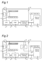
- a typical, prior art version of such an electrical device contains a Central Processing Unit (CPU) 3 for processing and controlling the whole electrical device, a Closely Coupled Memory (CCM) 5 for storing data and/or instructions, an external memory system 8 comprising external memory as well as a related external memory bus controller 13 and which external memory 8 is arranged for storing data and/or instructions.
- a clock unit 1 receives a master clock signal 2 for generating a main system clock signal 6 for the electrical device, i.e. for the CPU 3, the CCM 5 and the external memory 8.
- the device comprises an internal memory bus 4 for connecting the CPU 3 with the CCM 5, and an external memory bus 7 for connecting the CCM 5 with the external memory 8.
- the memory bus controller 13 is integrated on the chip and is connected to the CPU 3 to receive read and write instructions from CPU 3. After having received a read request from CPU 3, memory bus controller 13 retrieves the requested data from external memory 7 for CCM 5.
- CCM 5 is arranged to receive that data and to store it at a predetermined memory location where CPU 3 can access it.
- the CPU 3, the clock unit 1, the CCM 5 and the memory bus controller 13 are integrated in one single chip 14 (embedded).
- the CCM 5 is the smallest and fastest type of memory.
- the CCM 5 is optimized for speed rather than size.
- the external memory 8 is connected to the CCM 5 through external memory bus 7.
- the external memory 8 can be cost optimized for size and is usually slower than the integrated CCM 5.
- the electrical device is clocked by master clock signal 2.
- the clock unit 1 converts the master clock signal 2 into a faster version of the master clock signal 2 (e.g. by a Phase Locked Loop) or a slower version of master clock signal 2 (e.g. by a Clock Divider).
- the input of clock unit 1 is the master clock signal 2 and the output of clock unit 1 is the main system clock signal 6.
- the main system clock signal 6 clocks the CPU 3, CCM 5, external memory controller 13 and external memory 8.
- the power Pccm active consumed by the CPU 3, CCM 5 and other components on the chip which are active when the device is active consists of two components. One being a static power consumption Pccm static and the second one being a dynamic power consumption Pccm dynamic , which is dependent on the speed on which the device is operated.
- Pccm active Pccm static + Pccm f clock dynamic
- the main system clock signal 6 is designed to be equal to or slower than the master clock signal 2 for the sake of conserving power.
- the dynamic power consumption of components which are active when the device is active such as CPU 3 and CCM 5 will be lower than the situation when the main system clock signal 6 is the same as the master clock signal 2.
- the processor 3 will fetch a high percentage of its instructions from CCM 5 over internal memory bus 4 (in the order of 90% or higher) and only few instructions need to be fetched from the external memory 8 over external memory bus 7.
- the average bus speed will be close to the speed of internal memory bus 4 as most instructions are fetched from the fast CCM 5. Fetching the remaining instructions from the external memory 8 is relatively slow, but since the number of instructions is limited this has a minor impact on the average bus speed.
- the power Pext active consumed by the external memory 8 while active consists of two components. One being the static power consumption Pext static which is always present when the device is active and the second one being the dynamic power consumption Pext dynamic , which is dependent on the speed the device is operated.
- Pext active Pext static + Pext f clock dynamic
- the total power consumption consumed by the external memory 8 while inactive consists of one component; i.e. the standby power consumption Pext standby .
- the total power Pext total consumed by the external memory device 8 is equal to the active power consumption Pext active multiplied by the relative active period T active (defined as part per unit time) plus the standby power consumption Pext standby multiplied by the relative standby period T standby (defined as part per unit time).
- the relative active period T active can be expressed as follows when retrieving N bytes.
- N bytes can consist of either the following items or a combination of the following items:
- the access format to the external memory is not limited to the above items.
- the object of the invention is to reduce the overall system power consumption while still operating the device at a suitable, acceptable speed.
- the invention is based on the insight that the lowest current consumption can be achieved by clocking the internal components at the lowest clock speed possible and the external memory at the highest speed possible.
- the device according to figure 2 comprises a separate clock unit 9 for generating a separate external clock signal 10 with an external clock frequency f clock,10 to the external memory 8.
- the clock unit 9 receives clock signal 2 as input signal and derives external clock signal 10 from that clock signal 2.
- the frequency f clock,10 of clock signal 10 can be controlled separately from the clock frequency f clock of the clock signal 6.
- the frequency f clock , 10 of clock signal 10 can be made higher than the clock frequency f clock of the clock signal 6.
- the external clock frequency f clock,10 should be made as high as possible.
- the clock unit 9 is arranged to produce external clock signal 10 with external clock frequency f clock,10 as close as possible to the clock frequency of clock signal 2.
- the clock unit 9 may, again be based on an implementation with a phase locked loop or a frequency divider. However, the invention is not restricted to such an embodiment.
- the bus controller 13 receives the clock signal 10 as an input signal and is arranged to operate the transfer of data from external memory 8 to CCM 5 via external memory bus 7 at a maximum possible frequency.
- FIG. 2 shows that both clock unit 1 and clock unit 9 receive clock signal 2 and produce their output clock signals based on this input signal.
- clock unit 1 may be coupled to the output of clock unit 9 such as to receive clock signal 10 as an input and derive its output clock signal from clock signal 10.
- clock signals 6 and 10 are not independently controlled.
- FIG. 3 shows an alternative embodiment of the invention.
- the same reference signs are used for the same components as in the preceding figures.
- the embodiment of figure 3 comprises a FIFO (First In First Out) buffer 11 between external memory bus 7 and CCM 5.
- the FIFO 11 is connected to external memory bus 7 and to a system bus 12 that is, at its other end, also connected to CCM 5.
- Bus controller 13 is connected to FIFO 11 too
- the system of figure 3 provides more flexibility because the FIFO arranges for synchronization of the speed of transfer of data at the output of external memory 8 to the speed of receipt of data at the input of CCM 5. By doing so, bus throughput differences between system bus 12 at the input of CCM 5 and external memory bus 12 at the output of external memory 8 are equalized.
- the way how such a FIFO operates is known to persons skilled in the art and does not need any further explanation here.
Priority Applications (4)
| Application Number | Priority Date | Filing Date | Title |
|---|---|---|---|
| EP09175962A EP2323009A1 (de) | 2009-11-13 | 2009-11-13 | Elektronische Vorrichtung mit geringerem Energieverbrauch und externer Speicher |
| EP10190744.2A EP2323008B1 (de) | 2009-11-13 | 2010-11-10 | Elektronische Vorrichtung mit geringerem Energieverbrauch und externer Speicher |
| US12/944,443 US8826063B2 (en) | 2009-11-13 | 2010-11-11 | Electronic device with reduced power consumption in external memory |
| RU2010146158/08A RU2010146158A (ru) | 2009-11-13 | 2010-11-12 | Электронное устройство с пониженным энергопотреблением во внешнем запоминающем устройстве |
Applications Claiming Priority (1)
| Application Number | Priority Date | Filing Date | Title |
|---|---|---|---|
| EP09175962A EP2323009A1 (de) | 2009-11-13 | 2009-11-13 | Elektronische Vorrichtung mit geringerem Energieverbrauch und externer Speicher |
Publications (1)
| Publication Number | Publication Date |
|---|---|
| EP2323009A1 true EP2323009A1 (de) | 2011-05-18 |
Family
ID=41650487
Family Applications (2)
| Application Number | Title | Priority Date | Filing Date |
|---|---|---|---|
| EP09175962A Withdrawn EP2323009A1 (de) | 2009-11-13 | 2009-11-13 | Elektronische Vorrichtung mit geringerem Energieverbrauch und externer Speicher |
| EP10190744.2A Active EP2323008B1 (de) | 2009-11-13 | 2010-11-10 | Elektronische Vorrichtung mit geringerem Energieverbrauch und externer Speicher |
Family Applications After (1)
| Application Number | Title | Priority Date | Filing Date |
|---|---|---|---|
| EP10190744.2A Active EP2323008B1 (de) | 2009-11-13 | 2010-11-10 | Elektronische Vorrichtung mit geringerem Energieverbrauch und externer Speicher |
Country Status (3)
| Country | Link |
|---|---|
| US (1) | US8826063B2 (de) |
| EP (2) | EP2323009A1 (de) |
| RU (1) | RU2010146158A (de) |
Families Citing this family (3)
| Publication number | Priority date | Publication date | Assignee | Title |
|---|---|---|---|---|
| US9144017B2 (en) * | 2013-03-14 | 2015-09-22 | Qualcomm Incorporated | Systems and methods for saving power in monitoring and tracking devices |
| CN103744501B (zh) * | 2013-12-11 | 2018-04-13 | 中国科学院深圳先进技术研究院 | 一种移动终端cpu调频的方法及装置 |
| US10447461B2 (en) * | 2015-12-01 | 2019-10-15 | Infineon Technologies Austria Ag | Accessing data via different clocks |
Citations (4)
| Publication number | Priority date | Publication date | Assignee | Title |
|---|---|---|---|---|
| US6384651B1 (en) * | 2000-03-28 | 2002-05-07 | Intel Corporation | Method of generating a signal with controlled duty-cycle and pseudo-random spectrum |
| EP1653331A2 (de) * | 2004-10-29 | 2006-05-03 | STMicroelectronics Pvt. Ltd | Vorrichtung und Verfahren zum Eintreten und Beenden eines Niederstromverbrauchsmodus |
| US20070183192A1 (en) * | 2006-02-07 | 2007-08-09 | International Business Machines Corporation | Memory controller operating in a system with a variable system clock |
| US20080005607A1 (en) * | 2006-06-28 | 2008-01-03 | Matsushita Electric Industrial Co., Ltd. | Method of controlling information processing device, information processing device, program, and program converting method |
Family Cites Families (5)
| Publication number | Priority date | Publication date | Assignee | Title |
|---|---|---|---|---|
| US5604884A (en) * | 1993-03-22 | 1997-02-18 | Compaq Computer Corporation | Burst SRAMS for use with a high speed clock |
| US6073223A (en) * | 1997-07-21 | 2000-06-06 | Hewlett-Packard Company | Memory controller and method for intermittently activating and idling a clock signal for a synchronous memory |
| US7171576B2 (en) * | 2003-04-09 | 2007-01-30 | International Business Machines Corporation | Method, apparatus and program storage device for providing clocks to multiple frequency domains using a single input clock of variable frequency |
| US7360106B2 (en) * | 2004-08-05 | 2008-04-15 | Matsushita Electric Industrial Co., Ltd. | Power-saving processing unit, power-saving processing method and program record medium |
| US7746724B2 (en) * | 2007-01-31 | 2010-06-29 | Qimonda Ag | Asynchronous data transmission |
-
2009
- 2009-11-13 EP EP09175962A patent/EP2323009A1/de not_active Withdrawn
-
2010
- 2010-11-10 EP EP10190744.2A patent/EP2323008B1/de active Active
- 2010-11-11 US US12/944,443 patent/US8826063B2/en active Active
- 2010-11-12 RU RU2010146158/08A patent/RU2010146158A/ru not_active Application Discontinuation
Patent Citations (4)
| Publication number | Priority date | Publication date | Assignee | Title |
|---|---|---|---|---|
| US6384651B1 (en) * | 2000-03-28 | 2002-05-07 | Intel Corporation | Method of generating a signal with controlled duty-cycle and pseudo-random spectrum |
| EP1653331A2 (de) * | 2004-10-29 | 2006-05-03 | STMicroelectronics Pvt. Ltd | Vorrichtung und Verfahren zum Eintreten und Beenden eines Niederstromverbrauchsmodus |
| US20070183192A1 (en) * | 2006-02-07 | 2007-08-09 | International Business Machines Corporation | Memory controller operating in a system with a variable system clock |
| US20080005607A1 (en) * | 2006-06-28 | 2008-01-03 | Matsushita Electric Industrial Co., Ltd. | Method of controlling information processing device, information processing device, program, and program converting method |
Also Published As
| Publication number | Publication date |
|---|---|
| US8826063B2 (en) | 2014-09-02 |
| EP2323008A3 (de) | 2011-10-05 |
| EP2323008B1 (de) | 2016-04-27 |
| EP2323008A2 (de) | 2011-05-18 |
| RU2010146158A (ru) | 2012-05-20 |
| US20110119522A1 (en) | 2011-05-19 |
Similar Documents
| Publication | Publication Date | Title |
|---|---|---|
| US5845108A (en) | Semiconductor memory device using asynchronous signal | |
| JP4265195B2 (ja) | 半導体装置 | |
| KR100692345B1 (ko) | 프로세서 전력 상태들을 고려하는 메모리 제어기 | |
| US7366816B2 (en) | Method and apparatus for adaptively adjusting the bandwidth of a data transmission channel having multiple buffered paths | |
| US6598139B2 (en) | Information processing apparatus | |
| US10990322B2 (en) | Memory buffer chip, memory system and method of controlling the memory buffer chip | |
| TWI494925B (zh) | 實作記憶體子系統中之寫入平準化的方法及裝置 | |
| JP2007200542A (ja) | 半導体メモリ装置を装着したメモリモジュールを有するシステム | |
| KR20090132871A (ko) | 반도체 장치 및 멀티-칩 패키지 | |
| JPWO2006030904A1 (ja) | 半導体装置、及び通信制御方法 | |
| EP2323009A1 (de) | Elektronische Vorrichtung mit geringerem Energieverbrauch und externer Speicher | |
| US20180059713A1 (en) | Semiconductor device | |
| US20070038795A1 (en) | Asynchronous bus interface and processing method thereof | |
| JP2003263405A (ja) | 非同期インタフェース装置及び非同期インタフェース方法 | |
| US8495409B2 (en) | Host controller, semiconductor device and method for setting sampling phase | |
| US6978391B2 (en) | Asynchronous bus interface circuit, method of controlling the circuit, microcomputer, and device controlling method | |
| EP1288771A2 (de) | Halbleiterintegrierte Schaltung mit der Funktion, die Speisung eines Taktgebersignals zu beginnen und zu stoppen | |
| AU4825600A (en) | Systems and methods for a disk controller memory architecture | |
| US20150049571A1 (en) | Memory control device, control method of memory control device, information processing apparatus | |
| US20050134594A1 (en) | System and method for controlling display of mobile terminal | |
| KR100460994B1 (ko) | 직접 메모리 액세스 기능을 구비한 광대역 입출력 장치 및그 방법 | |
| KR100361511B1 (ko) | 다기능 직렬 통신 인터페이스 장치 | |
| US20060212638A1 (en) | Motherboard and control method thereof | |
| JP2007172510A (ja) | Dma転送装置 | |
| US7916575B2 (en) | Configurable latching for asynchronous memories |
Legal Events
| Date | Code | Title | Description |
|---|---|---|---|
| PUAI | Public reference made under article 153(3) epc to a published international application that has entered the european phase |
Free format text: ORIGINAL CODE: 0009012 |
|
| AK | Designated contracting states |
Kind code of ref document: A1 Designated state(s): AT BE BG CH CY CZ DE DK EE ES FI FR GB GR HR HU IE IS IT LI LT LU LV MC MK MT NL NO PL PT RO SE SI SK SM TR |
|
| AX | Request for extension of the european patent |
Extension state: AL BA RS |
|
| RAP1 | Party data changed (applicant data changed or rights of an application transferred) |
Owner name: DIALOG SEMICONDUCTOR B.V. |
|
| 17P | Request for examination filed |
Effective date: 20111116 |
|
| 17Q | First examination report despatched |
Effective date: 20120123 |
|
| STAA | Information on the status of an ep patent application or granted ep patent |
Free format text: STATUS: THE APPLICATION IS DEEMED TO BE WITHDRAWN |
|
| 18D | Application deemed to be withdrawn |
Effective date: 20120605 |