EP2317536A2 - Detection device and particle beam device having a detection device - Google Patents
Detection device and particle beam device having a detection device Download PDFInfo
- Publication number
- EP2317536A2 EP2317536A2 EP10189439A EP10189439A EP2317536A2 EP 2317536 A2 EP2317536 A2 EP 2317536A2 EP 10189439 A EP10189439 A EP 10189439A EP 10189439 A EP10189439 A EP 10189439A EP 2317536 A2 EP2317536 A2 EP 2317536A2
- Authority
- EP
- European Patent Office
- Prior art keywords
- detector
- filter element
- particle beam
- detection device
- electromagnetic radiation
- Prior art date
- Legal status (The legal status is an assumption and is not a legal conclusion. Google has not performed a legal analysis and makes no representation as to the accuracy of the status listed.)
- Granted
Links
Images

Classifications
-
- H—ELECTRICITY
- H01—ELECTRIC ELEMENTS
- H01J—ELECTRIC DISCHARGE TUBES OR DISCHARGE LAMPS
- H01J37/00—Discharge tubes with provision for introducing objects or material to be exposed to the discharge, e.g. for the purpose of examination or processing thereof
- H01J37/02—Details
- H01J37/244—Detectors; Associated components or circuits therefor
-
- G—PHYSICS
- G01—MEASURING; TESTING
- G01N—INVESTIGATING OR ANALYSING MATERIALS BY DETERMINING THEIR CHEMICAL OR PHYSICAL PROPERTIES
- G01N23/00—Investigating or analysing materials by the use of wave or particle radiation, e.g. X-rays or neutrons, not covered by groups G01N3/00 – G01N17/00, G01N21/00 or G01N22/00
- G01N23/22—Investigating or analysing materials by the use of wave or particle radiation, e.g. X-rays or neutrons, not covered by groups G01N3/00 – G01N17/00, G01N21/00 or G01N22/00 by measuring secondary emission from the material
- G01N23/225—Investigating or analysing materials by the use of wave or particle radiation, e.g. X-rays or neutrons, not covered by groups G01N3/00 – G01N17/00, G01N21/00 or G01N22/00 by measuring secondary emission from the material using electron or ion
- G01N23/2251—Investigating or analysing materials by the use of wave or particle radiation, e.g. X-rays or neutrons, not covered by groups G01N3/00 – G01N17/00, G01N21/00 or G01N22/00 by measuring secondary emission from the material using electron or ion using incident electron beams, e.g. scanning electron microscopy [SEM]
- G01N23/2254—Measuring cathodoluminescence
-
- H—ELECTRICITY
- H01—ELECTRIC ELEMENTS
- H01J—ELECTRIC DISCHARGE TUBES OR DISCHARGE LAMPS
- H01J37/00—Discharge tubes with provision for introducing objects or material to be exposed to the discharge, e.g. for the purpose of examination or processing thereof
- H01J37/02—Details
- H01J37/20—Means for supporting or positioning the object or the material; Means for adjusting diaphragms or lenses associated with the support
-
- H—ELECTRICITY
- H01—ELECTRIC ELEMENTS
- H01J—ELECTRIC DISCHARGE TUBES OR DISCHARGE LAMPS
- H01J37/00—Discharge tubes with provision for introducing objects or material to be exposed to the discharge, e.g. for the purpose of examination or processing thereof
- H01J37/02—Details
- H01J37/22—Optical, image processing or photographic arrangements associated with the tube
- H01J37/226—Optical arrangements for illuminating the object; optical arrangements for collecting light from the object
- H01J37/228—Optical arrangements for illuminating the object; optical arrangements for collecting light from the object whereby illumination or light collection take place in the same area of the discharge
-
- G—PHYSICS
- G01—MEASURING; TESTING
- G01N—INVESTIGATING OR ANALYSING MATERIALS BY DETERMINING THEIR CHEMICAL OR PHYSICAL PROPERTIES
- G01N2223/00—Investigating materials by wave or particle radiation
- G01N2223/60—Specific applications or type of materials
- G01N2223/612—Specific applications or type of materials biological material
-
- H—ELECTRICITY
- H01—ELECTRIC ELEMENTS
- H01J—ELECTRIC DISCHARGE TUBES OR DISCHARGE LAMPS
- H01J2237/00—Discharge tubes exposing object to beam, e.g. for analysis treatment, etching, imaging
- H01J2237/244—Detection characterized by the detecting means
- H01J2237/2445—Photon detectors for X-rays, light, e.g. photomultipliers
-
- H—ELECTRICITY
- H01—ELECTRIC ELEMENTS
- H01J—ELECTRIC DISCHARGE TUBES OR DISCHARGE LAMPS
- H01J2237/00—Discharge tubes exposing object to beam, e.g. for analysis treatment, etching, imaging
- H01J2237/26—Electron or ion microscopes
- H01J2237/28—Scanning microscopes
- H01J2237/2803—Scanning microscopes characterised by the imaging method
- H01J2237/2808—Cathodoluminescence
Definitions
- the invention relates to a detection device and a particle beam device having a detection device.
- the invention relates to a scanning electron microscope or a transmission electron microscope, which is designed to have a detection device.
- the detection device according to the invention and the particle beam device according to the invention are used in particular to examine transparent objects, in particular biological objects. These include in particular biological thin sections and biological samples labeled by immunolabeling or quantum dots.
- Electron beam devices in particular a scanning electron microscope (hereinafter also referred to SEM) and/or a transmission electron microscope (hereinafter also referred to as TEM) are used for examining objects (samples) to obtain information about the properties and behavior of these objects under certain conditions.
- SEM scanning electron microscope
- TEM transmission electron microscope
- an electron beam (hereinafter also referred to as a primary electron beam) is generated by a beam generator and focused by a beam guidance system on an object to be examined.
- the primary electron beam is guided in a grid pattern by a deflecting device over a surface of the object to be examined.
- the electrons of the primary electron beam then interact with the material of the object to be examined.
- secondary electrons electrons are emitted from the surface of the object to be examined
- electrons of the primary electron beam are backscattered (so-called backscattered electrons).
- the secondary electrons and backscattered electrons are detected and used for image generation. This yields an image of the surface of the object to be examined.
- a primary electron beam is also generated by a beam generator and focused by a beam guidance system on an object to be examined.
- the primary electron beam passes through the object to be examined.
- the electrons of the primary electron beam interact with the material of the object to be examined.
- the electrons passing through the object to be examined are imaged by a system including an objective lens and a projective lens on a luminescent screen or on a detector (for example, a camera).
- the imaging is performed in the scanning mode of a TEM.
- Such a TEM is usually referred to as a STEM.
- the electrons passing through the object in a TEM are detected by a detector connected downstream from the object - starting from the beam generator toward the object along the optical axis of the TEM.
- the secondary electrons or backscattered electrons are detected with a detector, for example, which is situated inside the objective lens or in an area between the objective lens and the beam generator.
- a SEM having the features known above is known, in which a first detector and a second detector are offset from one another along the optical axis of the SEM for detecting the secondary electrons and backscattered electrons. Both the first detector and the second detector have an aperture.
- the first detector situated in the vicinity of the object to be examined is used to detect the electrons which emerge from the object to be examined at a relatively large solid angle whereas the second detector which is situated in the area of the beam generator is used to detect the electrons emerging from the object to be examined at a relatively small solid angle.
- these electrons pass through the aperture of the first detector which is provided for the passage of the primary electron beam.
- an SEM which also has the aforementioned features is also known from the prior art.
- This known SEM is also additionally provided with a first detector and with a second detector.
- the first detector and the second detector are offset from one another along an optical axis of the SEM.
- the first detector is provided with an adjustable aperture to mask out secondary electrons so they do not strike the first detector.
- a particle beam, for example, an electron beam, guided onto an object may also interact with the object (in addition to the interaction particles already mentioned above) in such a way that electromagnetic radiation occurs in the form of cathodoluminescence.
- properties of the material of the object may be determined, for example, the determination of recombination centers, lattice defects, impurities and phase formations.
- Electron beam devices using which cathodoluminescence is also analyzed are known from the prior art.
- a known electron beam device using which an object situated in a sample chamber is bombarded with an electron beam. Due to an interaction of the electron beam with the material of the object, the object emits light due to cathodoluminescence (hereinafter also referred to as cathodoluminescent light).
- the cathodoluminescent light is guided to a detector by an ellipsoidal mirror through a window situated in a wall of the sample chamber. The detector is thus situated outside of the sample chamber.
- an object situated in a sample chamber is also bombarded with an electron beam.
- the object emits cathodoluminescent light, which is guided via a waveguide out of the sample chamber and further to a detector.
- the cathodoluminescent light is therefore detected at a relatively great distance from the object emitting the cathodoluminescent light. This results in an inferior efficiency in detecting the cathodoluminescent light because the cathodoluminescent light is detected only in a very restricted solid angle with respect to the object. Thus a portion of the photons of the cathodoluminescent light is not detected by the detector. Furthermore, the path from the source of the emitted cathodoluminescent light (i.e., the object) to the detector is relatively long. Intensity losses occur due to this path alone, which has a negative effect on the signal detected by the detector overall. Furthermore, intensity losses also occur in the waveguides used. ln the known prior art, multiple waveguide elements linked together are also used, so intensity losses may also occur at a coupling point between two different waveguide elements.
- waveguides and the ellipsoidal mirror also has another disadvantage. Because of the waveguides or the ellipsoidal mirror used, a portion of the secondary electrons or backscattered electrons is obscured, so that they are no longer able to strike a detector. This results in poor imaging.
- each detector used in these electron beam devices is essentially designed to detect only interaction particles or to detect only electromagnetic radiation. Therefore, in the case of the known electron beam devices, multiple detectors are always provided to be able to detect both interaction particles and electromagnetic radiation. This results in a greater complexity with regard to construction and assembly of these electron beam devices because vacuum feed-throughs and control units must be provided for each detector.
- the object of the invention is therefore to provide a detection device and a particle beam device having a detection device, using which good efficiency in detecting interaction particles and electromagnetic radiation is ensured.
- this object is achieved by a detection device having the features of Claim 1.
- Another detection device according to the invention is provided by the features of Claim 2.
- a particle beam device according to the invention is defined by the features of Claim 10.
- a use according to the invention of the particle beam device is described by the features of Claim 13. Additional features of the invention are derived from the following description, the appended claims and/or the appended figures.
- a detection device having at least one detector for detecting electromagnetic radiation and/or interaction particles.
- interaction particles occur due to interactions of the particle beam with the object (more specifically, with the material of the object).
- the interaction particles are the backscattered electrons already mentioned above and/or the secondary electrons, but also transmission electrons.
- the object may thus also be designed to be so thin that interaction particles are transmitted through the object.
- the electromagnetic radiation is, for example, luminescence, for example, cathodoluminescence or fluorescence, which occurs due to irradiation of an object with the help of a particle beam or a light source.
- the detection device also has at least one filter element, which is transparent to the electromagnetic radiation.
- the filter element is designed in such a way that electromagnetic radiation is transmitted through the filter element.
- the filter element is situated movably between a first position and a second position. ln the first position, the filter element is situated in relation to the detector in such a way that the filter element prevents the interaction particles from striking the detector. ln the second position, the filter element is situated in relation to the detector in such a way that the filter element allows the interaction particles to strike the detector.
- the detection device has the advantage that the detector for detecting the electromagnetic radiation cannot be situated outside of a sample chamber of a particle beam device but instead may be situated inside the sample chamber. For this reason, the use of waveguides and vacuum bushings may be omitted in a particle beam device in which the detection device is used, for example, so that the losses of intensity described above do not occur in comparison with the prior art. The efficiency of the detection device according to the invention is increased in comparison with that of the prior art in this way.
- the detection device allows both interaction particles and electromagnetic radiation to be detected by means of the detector by using only a single detector. lt is thus not absolutely necessary to provide an additional detector for detecting interaction particles or electromagnetic radiation.
- the movably designed filter element is movable between a first position and a second position. ln the first position, the filter element is situated between an object to be examined and the detector in such a way that the filter element prevents the interaction particles from striking the detector.
- the interaction particles are practically filtered out. For example, they are decelerated in the filter element or are backscattered by the filter element. ln the second position, however, the filter element is no longer situated between an object and the detector, so that the filter element allows the interaction particles to strike the detector.
- the detection device also allows accurate differentiation of whether a detection signal detected by the detector has occurred because of interaction particles or because of electromagnetic radiation. lt is possible to separate a first detection signal, generated by the electromagnetic radiation, from a second detection signal, generated by interaction particles. ln this way the first detection signal generated by the detector in a measurement in which the filter element is in the first position (i.e., in the position in which only electromagnetic radiation strikes the detector) is subtracted from a second detection signal in a measurement in which the filter element is in the second position (i.e., in the position in which interaction particles and electromagnetic radiation strike the detector). This yields an unambiguous determination of a signal which is based essentially only on the interaction particles. This may be used for imaging.
- the invention makes it possible to situate the detector and the filter element very close to an object, for example, at a distance of approximately 5 mm to approximately 30 mm from the object.
- an object which is to be examined and is situated on a movably designed object holder is to be situated relatively close to the filter element, for example, at a distance of 0.2 mm to 3 mm from one another.
- the invention is not limited to the aforementioned range. Instead it is also possible in particular to situate an object to be examined directly on the filter element, as will be discussed in greater detail below. Due to the aforementioned systems, it is possible for the detector of the detection device according to the invention to cover a relatively large solid angle.
- the detector is capable of detecting a relatively large portion of the interaction particles originating from an object and of the electromagnetic radiation.
- both the filter element and the detector are designed to be much larger than an object, so it is possible for the detector to essentially completely cover the half-space directed toward the object to be examined. This is the half-space into which the electromagnetic radiation is emitted by an object or into which the interaction particles arrive from an object.
- the detector of the detection device according to the invention is able to detect a greater number of photons of the electromagnetic radiation and/or a greater number of interaction particles. The efficiency of the detector is therefore increased in comparison with the prior art.
- the invention also relates to a detection device having the features of Claim 2.
- This detection device may have one of the aforementioned features or combinations of features and will now also be explained in greater detail below.
- at least one detector is provided for detecting electromagnetic radiation.
- the electromagnetic radiation is, for example, luminescence, for example, cathodoluminescence or fluorescence, which occurs due to irradiation of an object with a particle beam or a light source.
- luminescence for example, cathodoluminescence or fluorescence
- interaction particles are generated when the particle beam strikes the object due to interactions of the particle beam with the object (more specifically, with the material of the object).
- the interaction particles are the above-mentioned backscattered electrons and/or secondary electrons but also transmission electrons.
- the detection device according to the invention has at least one filter element designed in such a way that electromagnetic radiation is transmitted through the filter element and interaction particles are not transmitted through the filter element.
- the filter element is designed as an object holder.
- the filter element is designed as a microscope slide, for example. This allows an object that is to be examined to be situated very close to the detector. This in turn results in an increased efficiency of the detector.
- the filter element is made of a nonluminescent material.
- a nonluminescent material as mentioned above and below is understood to refer to a material in which no luminescence at all or only a low luminescence occurs, such that the intensity of the low luminescence is not superimposed on and does not influence the electromagnetic radiation emitted by an object, in particular in interaction with a particle beam or in interaction with the light of a light source. Whether an influence is to be expected due to the low luminescence depends in particular on the object to be examined. If the intensity of the electromagnetic radiation emitted by the object is much greater than the intensity of the low luminescence of the filter element, then an influence is probably not to be expected.
- the filter element is made of silicon dioxide, for example. It has been found in experiments that silicon dioxide (also known as quartz glass) is surprisingly nonluminescent, according to the definition given above, at room temperature (approximately 23°C) or in a range of ⁇ 5°C deviating slightly from room temperature (i.e., approximately 18°C to 28°C). This has the following background. When a particle beam in the form of an electron beam strikes a semiconductor, electrons are lifted from the valence band into the conduction band, resulting in the formation of electron-hole pairs. As soon as an electron and a hole recombine, a photon is emitted and detected. The preceding also readily applies to direct semiconductors (for example, GaAs).
- the filter element may be designed as an opposing field grating. By applying a suitable voltage, it is possible to deflect interaction particles in such a way that they do not strike the detector.
- the detection device has a reflective unit, which is situated movably.
- the reflective unit is movable between at least one reflection position and at least one resting position. In the reflection position, the reflective unit reflects a portion of the electromagnetic radiation toward the detector.
- This embodiment is suitable in particular for examining an object which is transparent to electromagnetic radiation.
- the object may be transparent to electromagnetic radiation of the same wavelength range as the electromagnetic radiation emitted by the object.
- the electromagnetic radiation emitted by the object not toward the detector but rather in another direction, for example, in the direction opposite the detector is reflected by the reflective unit onto the detector, so that the electromagnetic radiation is also transmitted through the object, for example, and then strikes the detector.
- the reflective unit is designed as a self-contained element, for example, a hemisphere, which, however, has a first aperture for admission of a particle beam.
- the reflective unit may be provided with a second aperture, through which the filter element is guided as it moves from the first position into the second position (and vice-versa).
- the detector has at least one first detector segment and at least one second detector segment.
- the first detector segment is used to detect interaction particles and electromagnetic radiation striking the detector at a first angle of incidence.
- the second detector segment is used for detecting interaction particles and electromagnetic radiation striking the detector at a second angle of incidence. lt is thus possible to draw conclusions about the dependence of the interaction particles and the electromagnetic radiation on the angle of incidence.
- These detector segments may be of any shape and configuration. For example, they may be designed as circular segments or ring segments and may detect the interaction particles or the electromagnetic radiation in the corresponding solid angle.
- the detection device has a moving device for moving the filter element.
- the moving device is designed in such a way that the filter element is movable back and forth between the first position and the second position. For example, the aforementioned movements take place in an interval in the range of 100 ms to 2 s. It is possible in this way to perform in particular time-resolved measurements for a preselected location on an object to be examined.
- the detector is designed as a semiconductor detector.
- the detector is designed as a photodiode, in particular as an avalanche photodiode.
- the detector may also be designed as a STEM detector.
- the invention also relates to a particle beam device having a detection device, which has at least one of the aforementioned features or a combination of at least two of the aforementioned features.
- the particle beam device according to the invention thus has the same advantages as those mentioned further above.
- the particle beam device according to the invention has a sample chamber. An object to be examined using the particle beam device is placed in the sample chamber.
- the particle beam device has a beam generator, which generates a particle beam, for example, an electron beam.
- the particle beam is focused on the object using an objective lens mounted on the particle beam device. When the particle beam strikes the object, interaction particles and electromagnetic radiation are generated due to interactions of the particle beam with the object (more specifically, with the material of the object).
- the interaction particles are not only the backscattered electrons and/or the secondary electrons already mentioned above, but also transmission electrons.
- the object may also be designed to be so thin that interaction particles are transmitted through the object.
- the electromagnetic radiation is, for example, cathodoluminescence.
- the electromagnetic radiation may additionally or alternatively also be generated by irradiation of the object to be examined using another light source.
- the particle beam device according to the invention is provided with the detection device according to the invention.
- the detector of the detection device is provided in the sample chamber. ln addition to this, for example, it is also provided that the filter element, the reflective unit and/or the moving device are also situated in the sample chamber.
- the detector is used to detect the electromagnetic radiation and the interaction particles.
- the filter element which is transparent to the electromagnetic radiation is provided. ln other words the filter element is designed in such a way that the electromagnetic radiation is transmitted through the filter element.
- the filter element is situated movably between the first position and the second position. ln the first position, the filter element is situated in relation to the detector, so that the filter element prevents the interaction particles from striking the detector. In the second position, the filter element is situated in relation to the detector in such a way that the filter element allows the interaction particles to strike the detector.
- the detector is used to detect the electromagnetic radiation.
- the filter element is designed in such a way that the electromagnetic radiation is transmitted through the filter element and the interaction particles are not transmitted through the filter element.
- the filter element is designed as an object holder.
- the filter element is designed as a microscope slide. This makes it possible to place the detector and the object to be examined in close proximity to one another. This in turn results in an increased efficiency of the detector.
- the particle beam device has an optical axis and that - starting from the beam generator - the object is situated first along the optical axis and then the detector. ln the first position, in which the filter element prevents the interaction particles from striking the detector, the filter element is situated between the detector and the object on the optical axis.
- This embodiment is suitable in particular for examining very thin objects because in this way either the electromagnetic radiation emitted by the thin object or the particles transmitted through the thin object are detected. For example, objects having a thickness from a few nm to several ⁇ m, for example, 10 nm to 5 ⁇ m, are examined.
- the invention also relates to a use of a particle beam device or a detection device having one of the aforementioned features or having one of the aforementioned combinations of features for examining a transparent object, in particular a biological object.
- the particle beam device according to the invention is suitable in particular for examining biological thin sections and/or biological samples, for example labeled by fluorescence markers, immunolabeling or quantum dots.
- the luminescence of the object in this examination for example, in the form of cathodoluminescence or fluorescence, is detected in a predefinable solid angle, for example, in a solid angle of 4 ⁇ .
- the invention also relates to another particle beam device, which may have at least one of the aforementioned features or combination of features and is explained in greater detail below.
- the particle beam device again has a sample chamber. An object which is examined using the particle beam device is placed in the sample chamber. Furthermore, the particle beam device has a beam generator, which generates a particle beam, for example, an electron beam. The particle beam is focused on the object using an objective lens mounted on the particle beam device.
- interaction particles and electromagnetic radiation occur due to interactions of the particle beam with the object.
- the interaction particles are the backscattered electrons, the secondary electrons and/or the transmission electrons already mentioned above.
- the electromagnetic radiation is cathodoluminescence, for example.
- the particle beam device has at least one filter element, which is transparent to the interaction particles.
- the filter element is designed in such a way that the interaction particles are transmitted through the filter element.
- the filter element is situated to move between a first position and a second position. ln the first position, the filter element is positioned in relation to the detector, in such a way that the filter element prevents the electromagnetic radiation from striking the detector. ln the second position, the filter element is situated relative to the detector, in such a way that the filter element allows the electromagnetic radiation to strike the detector.
- the aforementioned additional particle beam device according to the invention has the same advantages as those already mentioned above, with the difference that the filter element in the additional particle beam device according to the invention is used for filtering the electromagnetic radiation.
- the filter element in the additional particle beam device according to the invention is used for filtering the electromagnetic radiation.
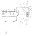
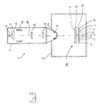
- FIG. 1 shows a schematic view of a first exemplary embodiment of a particle beam device 1 according to the invention.
- Particle beam device 1 has a particle beam column 2, which is situated on a sample chamber 3.
- Particle beam column 2 is designed as an electron beam column.
- Particle beam column 2 has a beam generator 4 in the form of an electron source (cathode) and a system, which includes a first electrode 5 and a second electrode 6. Second electrode 6 forms one end of a beam guidance tube (not shown).
- beam generator 4 is designed as a thermal field emitter. Electrons exiting from beam generator 4 are accelerated to a preselectable potential because of a potential difference between beam generator 4 and second electrode 6 (for example, to an energy in the range of 1 keV to 300 keV) and form a primary electron beam which is guided by a beam guidance system 16.
- the beam guidance tube is guided through an aperture of a magnetic lens acting as an objective lens 7.
- Objective lens 7 is provided with pole shoes (not shown) in which coils (not shown) are situated.
- scanning means 8 are provided, by which the primary electron beam is deflected and may be scanned over an object 9 placed in the sample chamber 3.
- first detector system of particle beam device 1 Secondary electrons and/or backscattered electrons generated due to the interaction of the primary electron beam with object 9 are detected by a first detector system of particle beam device 1 for the imaging.
- a first detector 10 is provided at the object end along optical axis 11 of particle beam column 2, while a second detector 12 is provided at the source end along optical axis 11 (i.e., toward beam generator 4).
- first detector 10 and second detector 12 are offset from one another.
- the aforementioned first detector system, including first detector 10 and second detector 12 is not absolutely essential for the invention. However, it may readily be provided as shown here.
- a second detector system is provided with particle beam device 1.
- a filter element 13 and finally a third detector 14 are positioned along optical axis 11.
- Filter element 13 and third detector 14 are part of a detection device 22 according to the invention, which is provided in particle beam device 1.
- Third detector 14 has the following function. When the primary electron beam strikes object 9, not only are the secondary electrons and backscattered electrons mentioned above generated due to the interactions of the primary electron beam with object 9, but also electromagnetic radiation occurs in the form of cathodoluminescent light. If object 9 is designed to be thin enough, then some electrons of the primary electron beam will also pass through object 9 (transmission electrons). Third detector 14 is then used only for detecting the electromagnetic radiation and the transmission electrons.
- electromagnetic radiation is generated by excitation of object 9 by a light source.
- Filter element 13 having a thickness of approximately 0.5 mm is transparent to the electromagnetic radiation (for example, in a wavelength range of 185 nm to 2.5 ⁇ m). ln other words, filter element 13 is designed in such a way that electromagnetic radiation is transmitted through filter element 13. However, filter element 13 is not transparent to the transmission electrons.
- Filter element 13 is situated movably between a first position A and a second position B.
- a moving device 15 which is part of detection device 22 and is situated outside of sample chamber 3 is provided. Moving device 15 is connected to filter element 13. lt is capable of moving filter element 13 from a first position A into a second position B (and vice-versa). Filter element 13 is shown in dotted lines in second position B.
- ln first position A filter element 13 is situated between object 9 and third detector 14. ln this position, filter element 13 prevents the transmission electrons from striking third detector 14. Thus only electromagnetic radiation strikes third detector 14 and is detected by it. ln second position B, filter element 13 is no longer situated between object 9 and third detector 14. In this position, both the electromagnetic radiation and the transmission electrons now strike third detector 14.
- a first detection signal which has been ascertained by third detector 14 in first position A and is based on the detected electromagnetic radiation, is subtracted from a second detection signal which was ascertained using third detector 14 in second position B and which is a summation signal based on the electromagnetic radiation and the transmission electrons. This yields a detection signal corrected for the electromagnetic radiation and based fundamentally only on the transmission electrons.
- Filter element 13 is made of a nonluminescent material, reference being made here to the definition given above in this regard.
- very pure silicon dioxide which is distributed under the brand name LITHOSIL Q1 by Schott, is used as the material. This material has proven to be particularly nonluminescent. This makes it possible for only the electromagnetic radiation emitted by object 9 to be detected by third detector 14. The measurement results thus achieved are therefore not subject to any great errors.
- Third detector 14 is segmented and has a plurality of detector segments, namely a first detector segment S1, a second detector segment S2, a third detector segment S3, a fourth detector segment S4, a fifth detector segment S5, a sixth detector segment S6, a seventh detector segment S7 and an eighth detector segment S8.
- Aforementioned detector segments S1 through S8 are used to detect the transmission electrons and the electromagnetic radiation striking third detector 14 at various angles of incidence.
- These detector segments may be formed as circular segments or as ring segments, for example. As an alternative, however, they may also have any other shape. lt is thus possible to obtain information about the dependence of the transmission electrons and the electromagnetic radiation on the angle of incidence.
- Moving device 15 of the embodiment presented here is designed in such a way that filter element 13 is movable back and forth relatively between first position A and second position B.
- filter element 13 may be moved back and forth between first position A and second position B in a very short interval, in particular an interval in the range of 100 ms to 2 s. This makes it possible to perform in particular time-resolved measurements for a preselectable location on object 9.
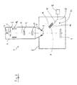
- FIG 2 shows a schematic view of a second exemplary embodiment of a particle beam device 1 according to the invention.
- Particle beam device 1 according to Figure 2 is based on particle beam device 1 according to Figure 1 .
- the same components are therefore labeled with the same reference numerals.
- the only difference between particle beam device 1 according to Figure 2 and particle beam device 1 according to Figure 1 is the placement of moving device 15, which is situated in sample chamber 3, in particle beam device 1 according to Figure 2 . lt is therefore no longer necessary to provide vacuum feed-throughs for moving device 15.
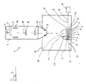
- FIG 3 shows a schematic view of a third exemplary embodiment of a particle beam device 1 according to the invention.
- Particle beam device 1 according to Figure 3 is based on particle beam device 1 according to Figure 1 .
- the same components are therefore provided with the same reference numerals.
- Particle beam device 1 according to Figure 3 additionally has a reflective unit 17 which belongs to the detection device 22 and is designed as a hemisphere having a maximum diameter in the range of 0.3 cm to 30 cm.
- Reflective unit 17 has a first through opening 18 through which the primary electron beam may pass toward object 9.
- a second through opening 19 through which filter element 13 may be brought from first position A into second position B (and vice-versa) is provided on reflective unit 17.
- reflective unit 17 On its side facing inward, reflective unit 17 has a reflective layer 20 produced by polishing aluminum, for example.
- a reflective layer 20 produced by polishing aluminum, for example.
- Reflective unit 17 is situated movably. Reflective unit 17 is movable between a reflection position and a resting position. ln the reflection position, reflective unit 17 covers object 9, third detector 14, and filter element 13 if it is in first position A. In the resting position, reflective unit 17 is moved, for example, in a direction perpendicular to optical axis 11 and running into the plane of the page. ln the resting position, reflective unit 17 no longer covers object 9 and third detector 14.
- Object 9 of this exemplary embodiment is transparent to the electromagnetic radiation.
- Object 9 is transparent here to the electromagnetic radiation of a wavelength range in which the wavelength of the electromagnetic radiation emitted by object 9 also occurs.
- the electromagnetic radiation emitted by object 9 not toward the third director 14 but rather in the direction opposite third detector 14 is reflected on the reflective layer 20, passing through object 9 and through filter element 13 and then striking third detector 14. It is thus possible to detect not only the electromagnetic radiation emitted into the first half-space directed to third detector 14 but also to detect the electromagnetic radiation emitted in the second half-space opposite the first half-space. ln this way, detection of the electromagnetic radiation over the total solid angle (4 ⁇ detection) is possible.
- reflective unit 17 is designed in such a way that object 9, filter element 13, detector 14 and moving device 15 are covered by reflective unit 17. Thus in this embodiment it is not absolutely necessary for reflective unit 17 to be moved. In the aforementioned embodiment, however, object 9 is designed to be much smaller than detector 14. Furthermore, if object 9, because of its thickness or because of the material of which it is made, is not transparent to electromagnetic radiation, detector 14 is nevertheless able to detect electromagnetic radiation emitted from the surface of object 9 and reflected by reflective unit 17.
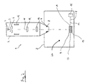
- FIG. 4 shows a schematic view of a fourth exemplary embodiment of a particle beam device 1 according to the invention.
- Particle beam device 1 according to Figure 4 is based on particle beam device 1 according to Figure 1 .
- the same components are therefore labeled with the same reference numerals.
- Particle beam device 1 according to Figure 4 differs from particle beam device 1 according to Figure 1 in that third detector 14 and filter element 13 are situated offset by an angle of approximately 45° to optical axis 11 in an area between object 9 and objective lens 7.
- moving device 15 is provided, so that filter element 13 is movable back and forth between first position A and second position B.
- third detector 14 is designed for detecting electromagnetic radiation, secondary electrons and backscattered electrons. Filter element 13 is used to filter the secondary electrons and the backscattered electrons.
- FIG. 5 shows a schematic view of a fifth exemplary embodiment of a particle beam device 1 according to the invention.
- Particle beam device 1 according to Figure 5 is based on particle beam device 1 according to Figure 1 .
- the same components are therefore labeled with the same reference numerals.
- Particle beam device 1 according to Figure 5 differs from particle beam device 1 according to Figure 1 in that filter element 13 is designed as an object holder in which object 9 is embedded.
- Filter element 13 is in the form of a microscope slide.
- filter element 13 is not designed to be movable. lt is used to filter the transmission electrons.
- the exemplary embodiments according to Figures 1 through 3 may also be designed as variants of the invention. ln these variants, filter element 13 filters the electromagnetic radiation instead of the transmission electrons. The interaction particles are thus transmitted through filter element 13. ln first position A of filter element 13, the electromagnetic radiation is prevented from striking third detector 14, so that in second position B, filter element 13 is situated in relation to third detector 14 in such a way that filter element 13 allows electromagnetic radiation to strike third detector 14.
- the exemplary embodiment according to Figure 4 may also be designed as described above, but with the difference that filter element 13 allows secondary electrons and backscattered electrons to pass through.
- the exemplary embodiment according to Figure 5 may also be designed like the variants from Figures 1 and 2 , but with the difference that filter element 13 is not movable in the exemplary embodiment according to Figure 5 .
- FIG. 6 shows a schematic view of a sixth exemplary embodiment of a particle beam device 1 according to the invention.
- Particle beam device 1 according to Figure 6 is based on particle beam device 1 according to Figure 1 .
- the same components are therefore labeled with the same reference numerals. Therefore, reference is made first to the statements made above.
- the only difference between particle beam device 1 according to Figure 6 and particle beam device 1 according to Figure 1 is the use of an opposing field grid 13A as the filter element, which is situated on a holding device 21 and which, by means of a moving device 15, is movable from first position A into second position B (and vice-versa).
- By applying a suitable voltage to opposing field grid 13A it is possible to deflect transmission electrons in such a way that they do not strike third detector 14. However, the electromagnetic radiation emitted by object 9 does strike third detector 14 and is detected. If opposing field grid 13A is in second position B, then transmission electrons passing through object 9 also strike third detector 14.
Landscapes
- Chemical & Material Sciences (AREA)
- Analytical Chemistry (AREA)
- Physics & Mathematics (AREA)
- Health & Medical Sciences (AREA)
- Life Sciences & Earth Sciences (AREA)
- Biochemistry (AREA)
- General Health & Medical Sciences (AREA)
- General Physics & Mathematics (AREA)
- Immunology (AREA)
- Pathology (AREA)
- Analysing Materials By The Use Of Radiation (AREA)
- Investigating, Analyzing Materials By Fluorescence Or Luminescence (AREA)
- Measurement Of Radiation (AREA)
Abstract
Description
- The invention relates to a detection device and a particle beam device having a detection device. In particular the invention relates to a scanning electron microscope or a transmission electron microscope, which is designed to have a detection device. The detection device according to the invention and the particle beam device according to the invention are used in particular to examine transparent objects, in particular biological objects. These include in particular biological thin sections and biological samples labeled by immunolabeling or quantum dots.
- Electron beam devices, in particular a scanning electron microscope (hereinafter also referred to SEM) and/or a transmission electron microscope (hereinafter also referred to as TEM) are used for examining objects (samples) to obtain information about the properties and behavior of these objects under certain conditions.
- In the case of an SEM, an electron beam (hereinafter also referred to as a primary electron beam) is generated by a beam generator and focused by a beam guidance system on an object to be examined. The primary electron beam is guided in a grid pattern by a deflecting device over a surface of the object to be examined. The electrons of the primary electron beam then interact with the material of the object to be examined. As a result of this interaction, in particular electrons are emitted from the surface of the object to be examined (so-called secondary electrons) and electrons of the primary electron beam are backscattered (so-called backscattered electrons). The secondary electrons and backscattered electrons are detected and used for image generation. This yields an image of the surface of the object to be examined.
- ln the case of a TEM, a primary electron beam is also generated by a beam generator and focused by a beam guidance system on an object to be examined. The primary electron beam passes through the object to be examined. As the primary electron beam passes through the object to be examined, the electrons of the primary electron beam interact with the material of the object to be examined. The electrons passing through the object to be examined are imaged by a system including an objective lens and a projective lens on a luminescent screen or on a detector (for example, a camera). ln addition, it is also possible to provide for detecting electrons backscattered on the object to be examined and/or secondary electrons emitted by the object to be examined by another detector to image an object to be examined. The imaging is performed in the scanning mode of a TEM. Such a TEM is usually referred to as a STEM.
- The electrons passing through the object in a TEM are detected by a detector connected downstream from the object - starting from the beam generator toward the object along the optical axis of the TEM.
- ln a SEM, the secondary electrons or backscattered electrons are detected with a detector, for example, which is situated inside the objective lens or in an area between the objective lens and the beam generator. For example, a SEM having the features known above is known, in which a first detector and a second detector are offset from one another along the optical axis of the SEM for detecting the secondary electrons and backscattered electrons. Both the first detector and the second detector have an aperture. The first detector situated in the vicinity of the object to be examined is used to detect the electrons which emerge from the object to be examined at a relatively large solid angle whereas the second detector which is situated in the area of the beam generator is used to detect the electrons emerging from the object to be examined at a relatively small solid angle. To arrive at the second detector, these electrons pass through the aperture of the first detector which is provided for the passage of the primary electron beam.
- Furthermore, an SEM which also has the aforementioned features is also known from the prior art. This known SEM is also additionally provided with a first detector and with a second detector. The first detector and the second detector are offset from one another along an optical axis of the SEM. The first detector is provided with an adjustable aperture to mask out secondary electrons so they do not strike the first detector.
- With regard to the prior art cited above, reference is made, for example, to
DE 198 28 476 A1 andDE 103 01 579 A1 . - A particle beam, for example, an electron beam, guided onto an object may also interact with the object (in addition to the interaction particles already mentioned above) in such a way that electromagnetic radiation occurs in the form of cathodoluminescence. By detecting and analyzing the cathodoluminescence (for example, by an intensity analysis and spectral analysis), properties of the material of the object may be determined, for example, the determination of recombination centers, lattice defects, impurities and phase formations. The preceding list is to be understood merely as an example and is not conclusive.
- Electron beam devices using which cathodoluminescence is also analyzed are known from the prior art. For example, there is a known electron beam device using which an object situated in a sample chamber is bombarded with an electron beam. Due to an interaction of the electron beam with the material of the object, the object emits light due to cathodoluminescence (hereinafter also referred to as cathodoluminescent light). The cathodoluminescent light is guided to a detector by an ellipsoidal mirror through a window situated in a wall of the sample chamber. The detector is thus situated outside of the sample chamber. In the case of another known electron beam device, using which cathodoluminescence is also analyzed, an object situated in a sample chamber is also bombarded with an electron beam. The object emits cathodoluminescent light, which is guided via a waveguide out of the sample chamber and further to a detector.
- ln the known prior art, the cathodoluminescent light is therefore detected at a relatively great distance from the object emitting the cathodoluminescent light. This results in an inferior efficiency in detecting the cathodoluminescent light because the cathodoluminescent light is detected only in a very restricted solid angle with respect to the object. Thus a portion of the photons of the cathodoluminescent light is not detected by the detector. Furthermore, the path from the source of the emitted cathodoluminescent light (i.e., the object) to the detector is relatively long. Intensity losses occur due to this path alone, which has a negative effect on the signal detected by the detector overall. Furthermore, intensity losses also occur in the waveguides used. ln the known prior art, multiple waveguide elements linked together are also used, so intensity losses may also occur at a coupling point between two different waveguide elements.
- Using waveguides and the ellipsoidal mirror also has another disadvantage. Because of the waveguides or the ellipsoidal mirror used, a portion of the secondary electrons or backscattered electrons is obscured, so that they are no longer able to strike a detector. This results in poor imaging.
- Another disadvantage of the known electron beam devices in which the cathodoluminescent light is analyzed is that each detector used in these electron beam devices is essentially designed to detect only interaction particles or to detect only electromagnetic radiation. Therefore, in the case of the known electron beam devices, multiple detectors are always provided to be able to detect both interaction particles and electromagnetic radiation. This results in a greater complexity with regard to construction and assembly of these electron beam devices because vacuum feed-throughs and control units must be provided for each detector.
- With regard to the prior art cited above, reference is made to
DE 197 31 226 A1 ,EP 0 914 669 B1 andGB 1 369 314 - The object of the invention is therefore to provide a detection device and a particle beam device having a detection device, using which good efficiency in detecting interaction particles and electromagnetic radiation is ensured.
- According to the invention, this object is achieved by a detection device having the features of Claim 1. Another detection device according to the invention is provided by the features of Claim 2. A particle beam device according to the invention is defined by the features of
Claim 10. A use according to the invention of the particle beam device is described by the features ofClaim 13. Additional features of the invention are derived from the following description, the appended claims and/or the appended figures. - According to Claim 1 of the invention, a detection device having at least one detector for detecting electromagnetic radiation and/or interaction particles is provided. For example, when a particle beam strikes an object, interaction particles occur due to interactions of the particle beam with the object (more specifically, with the material of the object). For example, the interaction particles are the backscattered electrons already mentioned above and/or the secondary electrons, but also transmission electrons. The object may thus also be designed to be so thin that interaction particles are transmitted through the object. The electromagnetic radiation is, for example, luminescence, for example, cathodoluminescence or fluorescence, which occurs due to irradiation of an object with the help of a particle beam or a light source. The detection device according to the invention also has at least one filter element, which is transparent to the electromagnetic radiation. ln other words, the filter element is designed in such a way that electromagnetic radiation is transmitted through the filter element. The filter element is situated movably between a first position and a second position. ln the first position, the filter element is situated in relation to the detector in such a way that the filter element prevents the interaction particles from striking the detector. ln the second position, the filter element is situated in relation to the detector in such a way that the filter element allows the interaction particles to strike the detector.
- The detection device according to the invention has the advantage that the detector for detecting the electromagnetic radiation cannot be situated outside of a sample chamber of a particle beam device but instead may be situated inside the sample chamber. For this reason, the use of waveguides and vacuum bushings may be omitted in a particle beam device in which the detection device is used, for example, so that the losses of intensity described above do not occur in comparison with the prior art. The efficiency of the detection device according to the invention is increased in comparison with that of the prior art in this way.
- Furthermore, the detection device according to the invention allows both interaction particles and electromagnetic radiation to be detected by means of the detector by using only a single detector. lt is thus not absolutely necessary to provide an additional detector for detecting interaction particles or electromagnetic radiation. In the case of the present invention, this is ensured by the fact that the movably designed filter element is movable between a first position and a second position. ln the first position, the filter element is situated between an object to be examined and the detector in such a way that the filter element prevents the interaction particles from striking the detector. The interaction particles are practically filtered out. For example, they are decelerated in the filter element or are backscattered by the filter element. ln the second position, however, the filter element is no longer situated between an object and the detector, so that the filter element allows the interaction particles to strike the detector.
- The detection device according to the invention also allows accurate differentiation of whether a detection signal detected by the detector has occurred because of interaction particles or because of electromagnetic radiation. lt is possible to separate a first detection signal, generated by the electromagnetic radiation, from a second detection signal, generated by interaction particles. ln this way the first detection signal generated by the detector in a measurement in which the filter element is in the first position (i.e., in the position in which only electromagnetic radiation strikes the detector) is subtracted from a second detection signal in a measurement in which the filter element is in the second position (i.e., in the position in which interaction particles and electromagnetic radiation strike the detector). This yields an unambiguous determination of a signal which is based essentially only on the interaction particles. This may be used for imaging.
- Due to the system comprising the detector and the filter element described here, the invention makes it possible to situate the detector and the filter element very close to an object, for example, at a distance of approximately 5 mm to approximately 30 mm from the object. In particular it is also provided that an object which is to be examined and is situated on a movably designed object holder, is to be situated relatively close to the filter element, for example, at a distance of 0.2 mm to 3 mm from one another. However, the invention is not limited to the aforementioned range. Instead it is also possible in particular to situate an object to be examined directly on the filter element, as will be discussed in greater detail below. Due to the aforementioned systems, it is possible for the detector of the detection device according to the invention to cover a relatively large solid angle. This is understood in particular to mean that the detector is capable of detecting a relatively large portion of the interaction particles originating from an object and of the electromagnetic radiation. For example, both the filter element and the detector are designed to be much larger than an object, so it is possible for the detector to essentially completely cover the half-space directed toward the object to be examined. This is the half-space into which the electromagnetic radiation is emitted by an object or into which the interaction particles arrive from an object. ln comparison with a detector according to the prior art situated outside of the sample chamber, the detector of the detection device according to the invention is able to detect a greater number of photons of the electromagnetic radiation and/or a greater number of interaction particles. The efficiency of the detector is therefore increased in comparison with the prior art.
- The invention also relates to a detection device having the features of Claim 2. This detection device may have one of the aforementioned features or combinations of features and will now also be explained in greater detail below. Again in the case of this detection device, at least one detector is provided for detecting electromagnetic radiation. The electromagnetic radiation is, for example, luminescence, for example, cathodoluminescence or fluorescence, which occurs due to irradiation of an object with a particle beam or a light source. When an object is irradiated by a particle beam, interaction particles are generated when the particle beam strikes the object due to interactions of the particle beam with the object (more specifically, with the material of the object). For example, the interaction particles are the above-mentioned backscattered electrons and/or secondary electrons but also transmission electrons. Furthermore, the detection device according to the invention has at least one filter element designed in such a way that electromagnetic radiation is transmitted through the filter element and interaction particles are not transmitted through the filter element. Furthermore, it is provided that the filter element is designed as an object holder. The filter element is designed as a microscope slide, for example. This allows an object that is to be examined to be situated very close to the detector. This in turn results in an increased efficiency of the detector. Reference is made to the preceding discussion with regard to additional advantages.
- ln another embodiment of the detection device according to the invention, it is additionally or alternatively provided that the filter element is made of a nonluminescent material. A nonluminescent material as mentioned above and below is understood to refer to a material in which no luminescence at all or only a low luminescence occurs, such that the intensity of the low luminescence is not superimposed on and does not influence the electromagnetic radiation emitted by an object, in particular in interaction with a particle beam or in interaction with the light of a light source. Whether an influence is to be expected due to the low luminescence depends in particular on the object to be examined. If the intensity of the electromagnetic radiation emitted by the object is much greater than the intensity of the low luminescence of the filter element, then an influence is probably not to be expected. An influence is probably also not to be expected if the low luminescence of the filter element occurs in a wavelength range, which is completely different from the wavelength range of the electromagnetic radiation emitted by the object. A measurement performed using the detector is thus not interfered with and the measurement results achieved are not subject to a great error. Therefore, this ensures that the electromagnetic radiation or at least the essential portion of the electromagnetic radiation emitted by the object to be examined is detected by the detector.
- In one embodiment of the invention, the filter element is made of silicon dioxide, for example. It has been found in experiments that silicon dioxide (also known as quartz glass) is surprisingly nonluminescent, according to the definition given above, at room temperature (approximately 23°C) or in a range of ±5°C deviating slightly from room temperature (i.e., approximately 18°C to 28°C). This has the following background. When a particle beam in the form of an electron beam strikes a semiconductor, electrons are lifted from the valence band into the conduction band, resulting in the formation of electron-hole pairs. As soon as an electron and a hole recombine, a photon is emitted and detected. The preceding also readily applies to direct semiconductors (for example, GaAs). For indirect semiconductors (for example, silicon), the preceding is not readily applicable. The greater the purity of the indirect semiconductor, the lower is the intensity of the emitted electromagnetic radiation when an electron beam strikes the indirect semiconductor. Furthermore, defect centers in the indirect semiconductor are filled with electrons due to the electron beam supplied. They are then no longer actively luminescent. Furthermore, the luminescence induced by an electron beam in a very pure silicon dioxide is a function of temperature. A fundamental luminescence is detectable essentially at temperatures below 220°K (i.e., below - 53.15°C). For example, synthetic quartz glass from the company Schott, distributed under the brand name LITHOSIL Q1, is a suitable nonluminescent material. This material is characterized by a high homogeneity and absence from inclusions and bubbles.
- In contrast with the aforementioned, it has been found in experiments that a variety of optically transparent materials used in the field of optics, for example, calcium fluoride (CaF2) or sapphire (Al2O3), are luminescent and therefore are unsuitable for the invention.
- Alternatively or in addition to this, the filter element may be designed as an opposing field grating. By applying a suitable voltage, it is possible to deflect interaction particles in such a way that they do not strike the detector.
- In yet another embodiment of the detection device according to the invention, it is additionally or alternatively provided that the detection device has a reflective unit, which is situated movably. The reflective unit is movable between at least one reflection position and at least one resting position. In the reflection position, the reflective unit reflects a portion of the electromagnetic radiation toward the detector. This embodiment is suitable in particular for examining an object which is transparent to electromagnetic radiation. For example, the object may be transparent to electromagnetic radiation of the same wavelength range as the electromagnetic radiation emitted by the object. The electromagnetic radiation emitted by the object not toward the detector but rather in another direction, for example, in the direction opposite the detector, is reflected by the reflective unit onto the detector, so that the electromagnetic radiation is also transmitted through the object, for example, and then strikes the detector. Thus, for example, it is possible to detect not only the electromagnetic radiation emitted into a first half-space directed toward the detector, but also to detect the electromagnetic radiation emitted into a second half-space opposite the first half-space. Detection of the electromagnetic radiation over the entire solid angle (4π detection) is thus fundamentally possible in this way. ln one embodiment, the reflective unit is designed as a self-contained element, for example, a hemisphere, which, however, has a first aperture for admission of a particle beam. Furthermore, the reflective unit may be provided with a second aperture, through which the filter element is guided as it moves from the first position into the second position (and vice-versa).
- ln another embodiment of the detection device according to the invention, it is additionally or alternatively provided that the detector has at least one first detector segment and at least one second detector segment. The first detector segment is used to detect interaction particles and electromagnetic radiation striking the detector at a first angle of incidence. However, the second detector segment is used for detecting interaction particles and electromagnetic radiation striking the detector at a second angle of incidence. lt is thus possible to draw conclusions about the dependence of the interaction particles and the electromagnetic radiation on the angle of incidence. These detector segments may be of any shape and configuration. For example, they may be designed as circular segments or ring segments and may detect the interaction particles or the electromagnetic radiation in the corresponding solid angle.
- ln another embodiment of the detection device according to the invention, it is additionally or alternatively provided that the detection device has a moving device for moving the filter element. The moving device is designed in such a way that the filter element is movable back and forth between the first position and the second position. For example, the aforementioned movements take place in an interval in the range of 100 ms to 2 s. It is possible in this way to perform in particular time-resolved measurements for a preselected location on an object to be examined.
- ln one embodiment of the detection device according to the invention, it is additionally or alternatively provided that the detector is designed as a semiconductor detector. For example, the detector is designed as a photodiode, in particular as an avalanche photodiode. Although it was already mentioned above, reference is made explicitly here to the fact that the detector is designed for detecting cathodoluminescence in particular. Again alternatively or additionally thereto, the detector may also be designed as a STEM detector.
- The invention also relates to a particle beam device having a detection device, which has at least one of the aforementioned features or a combination of at least two of the aforementioned features. The particle beam device according to the invention thus has the same advantages as those mentioned further above. The particle beam device according to the invention has a sample chamber. An object to be examined using the particle beam device is placed in the sample chamber. Furthermore, the particle beam device has a beam generator, which generates a particle beam, for example, an electron beam. The particle beam is focused on the object using an objective lens mounted on the particle beam device. When the particle beam strikes the object, interaction particles and electromagnetic radiation are generated due to interactions of the particle beam with the object (more specifically, with the material of the object). For example, the interaction particles are not only the backscattered electrons and/or the secondary electrons already mentioned above, but also transmission electrons. Thus the object may also be designed to be so thin that interaction particles are transmitted through the object. The electromagnetic radiation is, for example, cathodoluminescence. The electromagnetic radiation may additionally or alternatively also be generated by irradiation of the object to be examined using another light source. As mentioned above, the particle beam device according to the invention is provided with the detection device according to the invention. The detector of the detection device is provided in the sample chamber. ln addition to this, for example, it is also provided that the filter element, the reflective unit and/or the moving device are also situated in the sample chamber.
- ln another embodiment of the particle beam device according to the invention, the detector is used to detect the electromagnetic radiation and the interaction particles. ln addition, the filter element which is transparent to the electromagnetic radiation is provided. ln other words the filter element is designed in such a way that the electromagnetic radiation is transmitted through the filter element. The filter element is situated movably between the first position and the second position. ln the first position, the filter element is situated in relation to the detector, so that the filter element prevents the interaction particles from striking the detector. In the second position, the filter element is situated in relation to the detector in such a way that the filter element allows the interaction particles to strike the detector.
- ln an alternative embodiment of the particle beam device according to the invention, it is provided that the detector is used to detect the electromagnetic radiation. ln addition, the filter element is designed in such a way that the electromagnetic radiation is transmitted through the filter element and the interaction particles are not transmitted through the filter element. Furthermore, it is provided that the filter element is designed as an object holder. For example, the filter element is designed as a microscope slide. This makes it possible to place the detector and the object to be examined in close proximity to one another. This in turn results in an increased efficiency of the detector. With regard to the additional advantages, reference is made to the preceding discussion.
- ln yet another embodiment of the particle beam device according to the invention, it is additionally or alternatively provided that the particle beam device has an optical axis and that - starting from the beam generator - the object is situated first along the optical axis and then the detector. ln the first position, in which the filter element prevents the interaction particles from striking the detector, the filter element is situated between the detector and the object on the optical axis. This embodiment is suitable in particular for examining very thin objects because in this way either the electromagnetic radiation emitted by the thin object or the particles transmitted through the thin object are detected. For example, objects having a thickness from a few nm to several µm, for example, 10 nm to 5 µm, are examined.
- The invention also relates to a use of a particle beam device or a detection device having one of the aforementioned features or having one of the aforementioned combinations of features for examining a transparent object, in particular a biological object. For example, the particle beam device according to the invention is suitable in particular for examining biological thin sections and/or biological samples, for example labeled by fluorescence markers, immunolabeling or quantum dots. The luminescence of the object in this examination, for example, in the form of cathodoluminescence or fluorescence, is detected in a predefinable solid angle, for example, in a solid angle of 4π.
- The invention also relates to another particle beam device, which may have at least one of the aforementioned features or combination of features and is explained in greater detail below. The particle beam device again has a sample chamber. An object which is examined using the particle beam device is placed in the sample chamber. Furthermore, the particle beam device has a beam generator, which generates a particle beam, for example, an electron beam. The particle beam is focused on the object using an objective lens mounted on the particle beam device. When the particle beam strikes the object, interaction particles and electromagnetic radiation occur due to interactions of the particle beam with the object. For example, the interaction particles are the backscattered electrons, the secondary electrons and/or the transmission electrons already mentioned above. The electromagnetic radiation is cathodoluminescence, for example. Furthermore, at least one detector, which is situated in the sample chamber, is provided on the particle beam device. The detector is used for detecting the interaction particles. In addition, the particle beam device has at least one filter element, which is transparent to the interaction particles. ln other words, the filter element is designed in such a way that the interaction particles are transmitted through the filter element. The filter element is situated to move between a first position and a second position. ln the first position, the filter element is positioned in relation to the detector, in such a way that the filter element prevents the electromagnetic radiation from striking the detector. ln the second position, the filter element is situated relative to the detector, in such a way that the filter element allows the electromagnetic radiation to strike the detector. The aforementioned additional particle beam device according to the invention has the same advantages as those already mentioned above, with the difference that the filter element in the additional particle beam device according to the invention is used for filtering the electromagnetic radiation. For example, an aluminum foil having a foil thickness in the range of 10 nm to 20 nm, for example, is suitable as the filter element.
- The invention is explained in greater detail below on the basis of exemplary embodiments in the figures.
- Figure 1
- shows a schematic view of a first exemplary embodiment of a particle beam device according to the invention;
- Figure 2
- shows a schematic view of a second exemplary embodiment of a particle beam device according to the invention;
- Figure 3
- shows a schematic view of a third exemplary embodiment of a particle beam device according to the invention;
- Figure 4
- shows a schematic view of a fourth exemplary embodiment of a particle beam device according to the invention;
- Figure 5
- shows a schematic view of a fifth exemplary embodiment of a particle beam device according to the invention; as well as
- Figure 6
- shows a schematic view of a sixth exemplary embodiment of a particle beam device according to the invention.
-
Figure 1 shows a schematic view of a first exemplary embodiment of a particle beam device 1 according to the invention. Particle beam device 1 has a particle beam column 2, which is situated on asample chamber 3. Particle beam column 2 is designed as an electron beam column. - Particle beam column 2 has a
beam generator 4 in the form of an electron source (cathode) and a system, which includes afirst electrode 5 and asecond electrode 6.Second electrode 6 forms one end of a beam guidance tube (not shown). For example,beam generator 4 is designed as a thermal field emitter. Electrons exiting frombeam generator 4 are accelerated to a preselectable potential because of a potential difference betweenbeam generator 4 and second electrode 6 (for example, to an energy in the range of 1 keV to 300 keV) and form a primary electron beam which is guided by abeam guidance system 16. The beam guidance tube is guided through an aperture of a magnetic lens acting as anobjective lens 7.Objective lens 7 is provided with pole shoes (not shown) in which coils (not shown) are situated. Furthermore, scanning means 8 are provided, by which the primary electron beam is deflected and may be scanned over anobject 9 placed in thesample chamber 3. - Secondary electrons and/or backscattered electrons generated due to the interaction of the primary electron beam with
object 9 are detected by a first detector system of particle beam device 1 for the imaging. For this purpose, afirst detector 10 is provided at the object end alongoptical axis 11 of particle beam column 2, while asecond detector 12 is provided at the source end along optical axis 11 (i.e., toward beam generator 4). Furthermore,first detector 10 andsecond detector 12 are offset from one another. As already explained above, the aforementioned first detector system, includingfirst detector 10 andsecond detector 12, is not absolutely essential for the invention. However, it may readily be provided as shown here. - A second detector system is provided with particle beam device 1. Thus, starting from
beam generator 4 as seen towardobject 9,first object 9, then afilter element 13 and finally athird detector 14 are positioned alongoptical axis 11.Filter element 13 andthird detector 14 are part of adetection device 22 according to the invention, which is provided in particle beam device 1. -
Third detector 14 has the following function. When the primary electron beam strikesobject 9, not only are the secondary electrons and backscattered electrons mentioned above generated due to the interactions of the primary electron beam withobject 9, but also electromagnetic radiation occurs in the form of cathodoluminescent light. Ifobject 9 is designed to be thin enough, then some electrons of the primary electron beam will also pass through object 9 (transmission electrons).Third detector 14 is then used only for detecting the electromagnetic radiation and the transmission electrons. - ln an alternative embodiment (not shown), electromagnetic radiation is generated by excitation of
object 9 by a light source. -
Filter element 13 having a thickness of approximately 0.5 mm is transparent to the electromagnetic radiation (for example, in a wavelength range of 185 nm to 2.5 µm). ln other words,filter element 13 is designed in such a way that electromagnetic radiation is transmitted throughfilter element 13. However,filter element 13 is not transparent to the transmission electrons.Filter element 13 is situated movably between a first position A and a second position B. For this purpose, a movingdevice 15 which is part ofdetection device 22 and is situated outside ofsample chamber 3 is provided. Movingdevice 15 is connected to filterelement 13. lt is capable of movingfilter element 13 from a first position A into a second position B (and vice-versa).Filter element 13 is shown in dotted lines in second position B. - ln first position A,
filter element 13 is situated betweenobject 9 andthird detector 14. ln this position,filter element 13 prevents the transmission electrons from strikingthird detector 14. Thus only electromagnetic radiation strikesthird detector 14 and is detected by it. ln second position B,filter element 13 is no longer situated betweenobject 9 andthird detector 14. In this position, both the electromagnetic radiation and the transmission electrons now strikethird detector 14. To obtain a detection signal based essentially only on the transmission electrons, a first detection signal, which has been ascertained bythird detector 14 in first position A and is based on the detected electromagnetic radiation, is subtracted from a second detection signal which was ascertained usingthird detector 14 in second position B and which is a summation signal based on the electromagnetic radiation and the transmission electrons. This yields a detection signal corrected for the electromagnetic radiation and based fundamentally only on the transmission electrons. -
Filter element 13 is made of a nonluminescent material, reference being made here to the definition given above in this regard. In the exemplary embodiment presented here, very pure silicon dioxide, which is distributed under the brand name LITHOSIL Q1 by Schott, is used as the material. This material has proven to be particularly nonluminescent. This makes it possible for only the electromagnetic radiation emitted byobject 9 to be detected bythird detector 14. The measurement results thus achieved are therefore not subject to any great errors. -
Third detector 14 is segmented and has a plurality of detector segments, namely a first detector segment S1, a second detector segment S2, a third detector segment S3, a fourth detector segment S4, a fifth detector segment S5, a sixth detector segment S6, a seventh detector segment S7 and an eighth detector segment S8. Aforementioned detector segments S1 through S8 are used to detect the transmission electrons and the electromagnetic radiation strikingthird detector 14 at various angles of incidence. These detector segments may be formed as circular segments or as ring segments, for example. As an alternative, however, they may also have any other shape. lt is thus possible to obtain information about the dependence of the transmission electrons and the electromagnetic radiation on the angle of incidence. - Moving
device 15 of the embodiment presented here is designed in such a way that filterelement 13 is movable back and forth relatively between first position A and second position B. For example,filter element 13 may be moved back and forth between first position A and second position B in a very short interval, in particular an interval in the range of 100 ms to 2 s. This makes it possible to perform in particular time-resolved measurements for a preselectable location onobject 9. -
Figure 2 shows a schematic view of a second exemplary embodiment of a particle beam device 1 according to the invention. Particle beam device 1 according toFigure 2 is based on particle beam device 1 according toFigure 1 . The same components are therefore labeled with the same reference numerals. The only difference between particle beam device 1 according toFigure 2 and particle beam device 1 according toFigure 1 is the placement of movingdevice 15, which is situated insample chamber 3, in particle beam device 1 according toFigure 2 . lt is therefore no longer necessary to provide vacuum feed-throughs for movingdevice 15. -
Figure 3 shows a schematic view of a third exemplary embodiment of a particle beam device 1 according to the invention. Particle beam device 1 according toFigure 3 is based on particle beam device 1 according toFigure 1 . The same components are therefore provided with the same reference numerals. Particle beam device 1 according toFigure 3 additionally has areflective unit 17 which belongs to thedetection device 22 and is designed as a hemisphere having a maximum diameter in the range of 0.3 cm to 30 cm.Reflective unit 17 has a first through opening 18 through which the primary electron beam may pass towardobject 9. Furthermore, a second through opening 19 through whichfilter element 13 may be brought from first position A into second position B (and vice-versa) is provided onreflective unit 17. On its side facing inward,reflective unit 17 has areflective layer 20 produced by polishing aluminum, for example. However, reference is made explicitly to the fact that the invention is not limited to such areflective layer 20. lnstead, any suitablereflective layer 20 manufacturable by using suitable means and methods, for example, by sputtering or vapor deposition, may be used. -
Reflective unit 17 is situated movably.Reflective unit 17 is movable between a reflection position and a resting position. ln the reflection position,reflective unit 17 coversobject 9,third detector 14, andfilter element 13 if it is in first position A. In the resting position,reflective unit 17 is moved, for example, in a direction perpendicular tooptical axis 11 and running into the plane of the page. ln the resting position,reflective unit 17 no longer coversobject 9 andthird detector 14. - By means of
reflective unit 17, a portion of the electromagnetic radiation is reflected towardthird detector 14.Object 9 of this exemplary embodiment is transparent to the electromagnetic radiation.Object 9 is transparent here to the electromagnetic radiation of a wavelength range in which the wavelength of the electromagnetic radiation emitted byobject 9 also occurs. The electromagnetic radiation emitted byobject 9 not toward thethird director 14 but rather in the direction oppositethird detector 14 is reflected on thereflective layer 20, passing throughobject 9 and throughfilter element 13 and then strikingthird detector 14. It is thus possible to detect not only the electromagnetic radiation emitted into the first half-space directed tothird detector 14 but also to detect the electromagnetic radiation emitted in the second half-space opposite the first half-space. ln this way, detection of the electromagnetic radiation over the total solid angle (4π detection) is possible. - In an alternative embodiment (not shown),
reflective unit 17 is designed in such a way that object 9,filter element 13,detector 14 and movingdevice 15 are covered byreflective unit 17. Thus in this embodiment it is not absolutely necessary forreflective unit 17 to be moved. In the aforementioned embodiment, however,object 9 is designed to be much smaller thandetector 14. Furthermore, ifobject 9, because of its thickness or because of the material of which it is made, is not transparent to electromagnetic radiation,detector 14 is nevertheless able to detect electromagnetic radiation emitted from the surface ofobject 9 and reflected byreflective unit 17. -
Figure 4 shows a schematic view of a fourth exemplary embodiment of a particle beam device 1 according to the invention. Particle beam device 1 according toFigure 4 is based on particle beam device 1 according toFigure 1 . The same components are therefore labeled with the same reference numerals. To this extent, reference is made first to the preceding discussion. Particle beam device 1 according toFigure 4 differs from particle beam device 1 according toFigure 1 in thatthird detector 14 andfilter element 13 are situated offset by an angle of approximately 45° tooptical axis 11 in an area betweenobject 9 andobjective lens 7. Here again, movingdevice 15 is provided, so thatfilter element 13 is movable back and forth between first position A and second position B. ln the exemplary embodiment shown here,third detector 14 is designed for detecting electromagnetic radiation, secondary electrons and backscattered electrons.Filter element 13 is used to filter the secondary electrons and the backscattered electrons. -
Figure 5 shows a schematic view of a fifth exemplary embodiment of a particle beam device 1 according to the invention. Particle beam device 1 according toFigure 5 is based on particle beam device 1 according toFigure 1 . The same components are therefore labeled with the same reference numerals. To this extent, reference is made first to the preceding discussion. Particle beam device 1 according toFigure 5 differs from particle beam device 1 according toFigure 1 in thatfilter element 13 is designed as an object holder in which object 9 is embedded.Filter element 13 is in the form of a microscope slide. ln contrast with the exemplary embodiment according toFigure 1 ,filter element 13 is not designed to be movable. lt is used to filter the transmission electrons. - The exemplary embodiments according to
Figures 1 through 3 may also be designed as variants of the invention. ln these variants,filter element 13 filters the electromagnetic radiation instead of the transmission electrons. The interaction particles are thus transmitted throughfilter element 13. ln first position A offilter element 13, the electromagnetic radiation is prevented from strikingthird detector 14, so that in second position B,filter element 13 is situated in relation tothird detector 14 in such a way that filterelement 13 allows electromagnetic radiation to strikethird detector 14. The exemplary embodiment according toFigure 4 may also be designed as described above, but with the difference that filterelement 13 allows secondary electrons and backscattered electrons to pass through. The exemplary embodiment according toFigure 5 may also be designed like the variants fromFigures 1 and2 , but with the difference that filterelement 13 is not movable in the exemplary embodiment according toFigure 5 . -
Figure 6 shows a schematic view of a sixth exemplary embodiment of a particle beam device 1 according to the invention. Particle beam device 1 according toFigure 6 is based on particle beam device 1 according toFigure 1 . The same components are therefore labeled with the same reference numerals. Therefore, reference is made first to the statements made above. The only difference between particle beam device 1 according toFigure 6 and particle beam device 1 according toFigure 1 is the use of an opposingfield grid 13A as the filter element, which is situated on a holdingdevice 21 and which, by means of a movingdevice 15, is movable from first position A into second position B (and vice-versa). By applying a suitable voltage to opposingfield grid 13A, it is possible to deflect transmission electrons in such a way that they do not strikethird detector 14. However, the electromagnetic radiation emitted byobject 9 does strikethird detector 14 and is detected. If opposingfield grid 13A is in second position B, then transmission electrons passing throughobject 9 also strikethird detector 14. - The exemplary embodiments shown in the figures may have the effects and advantages already mentioned above, so that reference is made here to this discussion.
-
- 1
- Particle beam device
- 2
- Particle beam column
- 3
- Sample chamber
- 4
- Beam generator
- 5
- First electrode
- 6
- Second electrode
- 7
- Objective lens
- 8
- Scanning means
- 9
- Object
- 10
- First detector
- 11
- Optical axis
- 12
- Second detector
- 13
- Filter element
- 13A
- Opposing field grid
- 14
- Third detector
- 15
- Moving device
- 16
- Beam guidance system
- 17
- Reflective unit
- 18
- First through opening
- 19
- Second through opening
- 20
- Reflective layer
- 21
- Holding device
- 22
- Detection device
- A
- First position
- B
- Second position
- S1
- First detector segment
- S2
- Second detector segment
- S3
- Third detector segment
- S4
- Fourth detector segment
- S5
- Fifth detector segment
- S6
- Sixth detector segment
- S7
- Seventh detector segment
- S8
- Eighth detector segment
Claims (14)
- A detection device (22) comprising- at least one detector (14) for detecting electromagnetic radiation and/or interaction particles,- at least one filter element (13) through which the electromagnetic radiation is transmitted and which is designed for preventing the interaction particles from striking the detector (14),wherein- the filter element (13) is situated movably between a first position (A) and a second position (B),- the filter element (13) is situated in the first position (A) relative to the detector (14) in such a way that the filter element (13) prevents the interaction particles from striking the detector (14), and wherein- the filter element (13) is situated in the second position (B) relative to the detector (14) in such a way that the filter element (13) allows the interaction particles to strike the detector (14).
- A detection device (22), comprising- at least one detector (14) for detecting electromagnetic radiation,- at least one filter element (13) through which the electromagnetic radiation is transmitted and through which the interaction particles are not transmitted,wherein the filter element (13) is designed as an object holder.
- The detection device (22) as recited in Claim 1 or 2, wherein the filter element (13) is made of a nonluminescent material.
- The detection device (22) as recited in one of the preceding claims, wherein the filter element (13) is made of silicon dioxide.
- The detection device (22) as recited in one of the preceding claims, wherein- the detection device (22) has a reflective unit (17) which is situated movably between at least one reflection position and at least one resting position, wherein in the reflection position the reflective unit (17) reflects a portion of the electromagnetic radiation toward the detector (14).
- The detection device (22) as recited in one of the preceding claims, wherein the detector (14) has at least one first detector segment (S1 through S8) and at least one second detector segment (S1 through S8).
- The detection device (22) as recited in one of the preceding claims except in conjunction with Claim 2, wherein- the detection device (22) has a moving device (15) for moving the filter element (13), and wherein- the moving device (15) is designed in such a way that it allows the filter element (13) to move back and forth between the first position (A) and the second position (B) in a predefinable period of time, in particular in a period of time in the range from 100 ms to 2 s.
- The detection device (22) as recited in one of the preceding claims, wherein the detector (14) is designed as a semiconductor detector.
- The detection device (22) as recited in one of the preceding claims, wherein the detector (14) has at least one of the following properties:- the detector (14) is designed for detecting luminescence, in particular in the form of cathodoluminescence or fluorescence or- the detector (14) is designed as a STEM detector.
- A particle beam device (1) comprising- a sample chamber (3),- an object (9) situated in the sample chamber (3),- a beam generator (4, 16) for generating a particle beam,- an objective lens (7) for focusing the particle beam on the object (9), so that when the particle beam strikes the object (9), interaction particles and electromagnetic radiation occur due to the interactions of the particle beam with the object (9), and- at least one detection device (22) as recited in one of the preceding claims,wherein the detector (14) is situated in the sample chamber (3).
- The particle beam device (1) as recited in Claim 10, wherein the filter element (13), the reflective unit (17) and/or the moving device (15) is/are situated in the sample chamber (3).
- The particle beam device (1) as recited in Claim 10 or 11, wherein the particle beam device (1) comprises an optical axis (11), wherein first the object (9) and then the detector (14) are situated along the optical axis (11), starting from the beam generator (4) toward the object (9).
- A use of a detection device (22) or a particle beam device (1) as recited in one of the preceding claims for examining a transparent object (9), in particular a biological sample, wherein luminescence in particular in the form of cathodoluminescence or fluorescence is detected in a predefinable solid angle in the examination.
- The use as recited in Claim 13 in which the predefinable solid angle is up to 4π.
Applications Claiming Priority (1)
| Application Number | Priority Date | Filing Date | Title |
|---|---|---|---|
| DE102009046211.2A DE102009046211B4 (en) | 2009-10-30 | 2009-10-30 | Detection device and particle beam device with detection device |
Publications (3)
| Publication Number | Publication Date |
|---|---|
| EP2317536A2 true EP2317536A2 (en) | 2011-05-04 |
| EP2317536A3 EP2317536A3 (en) | 2013-10-02 |
| EP2317536B1 EP2317536B1 (en) | 2017-12-06 |
Family
ID=43734015
Family Applications (1)
| Application Number | Title | Priority Date | Filing Date |
|---|---|---|---|
| EP10189439.2A Active EP2317536B1 (en) | 2009-10-30 | 2010-10-29 | Detection device and particle beam device having a detection device |
Country Status (3)
| Country | Link |
|---|---|
| US (1) | US8513604B2 (en) |
| EP (1) | EP2317536B1 (en) |
| DE (1) | DE102009046211B4 (en) |
Cited By (3)
| Publication number | Priority date | Publication date | Assignee | Title |
|---|---|---|---|---|
| EP2690647A1 (en) * | 2012-07-26 | 2014-01-29 | David Stowe | System and method for measuring angular luminescence in a charged particle microscope |
| US8648301B2 (en) | 2011-09-22 | 2014-02-11 | Carl Zeiss Microscopy Ltd. | Particle beam system having a hollow light guide |
| EP3392650B1 (en) * | 2013-05-16 | 2022-08-31 | Carl Zeiss Microscopy GmbH | Device for spectroscopic analysis |
Families Citing this family (9)
| Publication number | Priority date | Publication date | Assignee | Title |
|---|---|---|---|---|
| EP2461348A1 (en) * | 2010-12-06 | 2012-06-06 | FEI Company | Detector system for use with transmission electron microscope spectroscopy |
| JP6239246B2 (en) * | 2013-03-13 | 2017-11-29 | 株式会社日立ハイテクノロジーズ | Charged particle beam apparatus, sample observation method, sample stage, observation system, and light emitting member |
| US9851312B2 (en) * | 2014-05-07 | 2017-12-26 | The Boeing Company | Backscatter inspection systems, and related methods |
| US10903042B2 (en) | 2014-05-08 | 2021-01-26 | Technische Universiteit Delft | Apparatus and method for inspecting a sample using a plurality of charged particle beams |
| NL2012780B1 (en) * | 2014-05-08 | 2016-02-23 | Univ Delft Tech | Apparatus and method for inspecting a sample using a plurality of charged particle beams. |
| US10024799B2 (en) * | 2014-12-27 | 2018-07-17 | Indian Institute Of Science | Chemical signature resolved detection of concealed objects |
| DE102015210893B4 (en) * | 2015-06-15 | 2019-05-09 | Carl Zeiss Microscopy Gmbh | Analysis device for analyzing the charged particle energy and particle beam device with an analysis device |
| US10818471B2 (en) | 2015-12-22 | 2020-10-27 | Hitachi High-Tech Corporation | Charged particle beam device |
| WO2019232020A1 (en) * | 2018-05-30 | 2019-12-05 | Gatan, Inc. | Apparatus for wavelength resolved angular resolved cathodoluminescence |
Citations (5)
| Publication number | Priority date | Publication date | Assignee | Title |
|---|---|---|---|---|
| GB1369314A (en) | 1971-10-05 | 1974-10-02 | Oesterr Studien Atomenergie | Scanning electron microscopes having cathodoluminescence devices |
| DE19731226A1 (en) | 1997-02-25 | 1998-08-27 | Georg Dr Koschek | Cathodoluminescence spectrometer for electro-optic instruments |
| DE19828476A1 (en) | 1998-06-26 | 1999-12-30 | Leo Elektronenmikroskopie Gmbh | Particle beam device |
| EP0914669B1 (en) | 1996-07-01 | 2004-04-28 | K E Developments Limited | Detector devices |
| DE10301579A1 (en) | 2003-01-16 | 2004-07-29 | Leo Elektronenmikroskopie Gmbh | Electron beam device and detector arrangement |
Family Cites Families (11)
| Publication number | Priority date | Publication date | Assignee | Title |
|---|---|---|---|---|
| US4117323A (en) * | 1977-03-07 | 1978-09-26 | Iowa State University Research Foundation | Electron microscopes |
| NL8100449A (en) * | 1981-01-30 | 1982-08-16 | Philips Nv | ELECTRON MICROSCOPE WITH ROENTGEND DETECTOR. |
| IT1223998B (en) * | 1988-12-16 | 1990-09-29 | Sip | DETECTION SYSTEM FOR CATODOLUMINESCENCE ANALYSIS |
| US5264704A (en) * | 1992-11-17 | 1993-11-23 | National University Of Singapore | High efficiency cathodoluminescence detector with high discrimination against backscattered electrons |
| US6982431B2 (en) * | 1998-08-31 | 2006-01-03 | Molecular Devices Corporation | Sample analysis systems |
| US6885445B2 (en) * | 1998-05-09 | 2005-04-26 | Renishaw Plc | Electron microscope and spectroscopy system |
| GB0106342D0 (en) * | 2001-03-15 | 2001-05-02 | Renishaw Plc | Spectroscopy apparatus and method |
| JP2006040867A (en) * | 2004-06-23 | 2006-02-09 | Hoya Candeo Optronics株式会社 | Excimer lamp apparatus |
| NL1027462C2 (en) | 2004-11-09 | 2006-05-10 | Koninkl Philips Electronics Nv | Method for locating fluorescent markers. |
| EP1956633A3 (en) * | 2007-02-06 | 2009-12-16 | FEI Company | Particle-optical apparatus for simultaneous observing a sample with particles and photons |
| EP2194565A1 (en) * | 2008-12-03 | 2010-06-09 | FEI Company | Dark field detector for use in a charged-particle optical apparatus |
-
2009
- 2009-10-30 DE DE102009046211.2A patent/DE102009046211B4/en not_active Expired - Fee Related
-
2010
- 2010-10-27 US US12/925,704 patent/US8513604B2/en active Active
- 2010-10-29 EP EP10189439.2A patent/EP2317536B1/en active Active
Patent Citations (5)
| Publication number | Priority date | Publication date | Assignee | Title |
|---|---|---|---|---|
| GB1369314A (en) | 1971-10-05 | 1974-10-02 | Oesterr Studien Atomenergie | Scanning electron microscopes having cathodoluminescence devices |
| EP0914669B1 (en) | 1996-07-01 | 2004-04-28 | K E Developments Limited | Detector devices |
| DE19731226A1 (en) | 1997-02-25 | 1998-08-27 | Georg Dr Koschek | Cathodoluminescence spectrometer for electro-optic instruments |
| DE19828476A1 (en) | 1998-06-26 | 1999-12-30 | Leo Elektronenmikroskopie Gmbh | Particle beam device |
| DE10301579A1 (en) | 2003-01-16 | 2004-07-29 | Leo Elektronenmikroskopie Gmbh | Electron beam device and detector arrangement |
Cited By (3)
| Publication number | Priority date | Publication date | Assignee | Title |
|---|---|---|---|---|
| US8648301B2 (en) | 2011-09-22 | 2014-02-11 | Carl Zeiss Microscopy Ltd. | Particle beam system having a hollow light guide |
| EP2690647A1 (en) * | 2012-07-26 | 2014-01-29 | David Stowe | System and method for measuring angular luminescence in a charged particle microscope |
| EP3392650B1 (en) * | 2013-05-16 | 2022-08-31 | Carl Zeiss Microscopy GmbH | Device for spectroscopic analysis |
Also Published As
| Publication number | Publication date |
|---|---|
| DE102009046211B4 (en) | 2017-08-24 |
| DE102009046211A1 (en) | 2011-05-26 |
| US20110220793A1 (en) | 2011-09-15 |
| EP2317536A3 (en) | 2013-10-02 |
| EP2317536B1 (en) | 2017-12-06 |
| US8513604B2 (en) | 2013-08-20 |
Similar Documents
| Publication | Publication Date | Title |
|---|---|---|
| EP2317536B1 (en) | Detection device and particle beam device having a detection device | |
| US11087955B2 (en) | System combination of a particle beam system and a light-optical system with collinear beam guidance, and use of the system combination | |
| KR102410589B1 (en) | Method for alignment of a light beam to a charged particle beam | |
| US8895921B2 (en) | Inspection apparatus and replaceable door for a vacuum chamber of such an inspection apparatus and a method for operating an inspection apparatus | |
| TWI631722B (en) | Light multiplier tube, image sensor and detection system using photomultiplier tube (PMT) or image sensor | |
| US8648301B2 (en) | Particle beam system having a hollow light guide | |
| JP6169506B2 (en) | Specimen holder, observation system, and image generation method | |
| JP5947928B2 (en) | Adaptive cathodoluminescence detection system and microscope employing such a system | |
| JP2000513487A (en) | Detector | |
| JP4354197B2 (en) | Scanning electron microscope | |
| WO2015185995A1 (en) | Charged particle beam device | |
| WO2013175972A1 (en) | Electron microscope and electron detector | |
| US9029768B2 (en) | Detector and charged particle beam instrument | |
| JP2013026152A (en) | Electron microscope | |
| CN116046821B (en) | A backscattered electron scintillator detector device and detection method | |
| EP1898443B1 (en) | Asymmetric annular detector | |
| JP4135219B2 (en) | Charged particle beam projection optical system | |
| JP5822614B2 (en) | Inspection device | |
| KR101727196B1 (en) | Infrared-electron correlative microscope | |
| JP7580803B2 (en) | Apparatus and method for detecting one or more scanned charged particle beams - Patents.com | |
| JP6228870B2 (en) | Detector and charged particle beam device | |
| RU2452052C1 (en) | Nano-resolution x-ray microscope | |
| WO2024025413A1 (en) | Method and apparatus for in-situ sample quality inspection in cryogenic focused ion beam milling | |
| WO2001084590A2 (en) | Method and apparatus for imaging a specimen using indirect in-column detection of secondary electrons in a microcolumn | |
| TW201235796A (en) | Methods, systems and apparatus for monitoring integrity of an article, EUV optical apparatus incorporating the same |
Legal Events
| Date | Code | Title | Description |
|---|---|---|---|
| PUAI | Public reference made under article 153(3) epc to a published international application that has entered the european phase |
Free format text: ORIGINAL CODE: 0009012 |
|
| AK | Designated contracting states |
Kind code of ref document: A2 Designated state(s): AL AT BE BG CH CY CZ DE DK EE ES FI FR GB GR HR HU IE IS IT LI LT LU LV MC MK MT NL NO PL PT RO RS SE SI SK SM TR |
|
| AX | Request for extension of the european patent |
Extension state: BA ME |
|
| PUAL | Search report despatched |
Free format text: ORIGINAL CODE: 0009013 |
|
| AK | Designated contracting states |
Kind code of ref document: A3 Designated state(s): AL AT BE BG CH CY CZ DE DK EE ES FI FR GB GR HR HU IE IS IT LI LT LU LV MC MK MT NL NO PL PT RO RS SE SI SK SM TR |
|
| AX | Request for extension of the european patent |
Extension state: BA ME |
|
| RIC1 | Information provided on ipc code assigned before grant |
Ipc: H01J 37/244 20060101AFI20130823BHEP Ipc: G01N 23/225 20060101ALI20130823BHEP Ipc: H01J 37/20 20060101ALI20130823BHEP Ipc: H01J 37/22 20060101ALI20130823BHEP |
|
| 17P | Request for examination filed |
Effective date: 20140331 |
|
| RBV | Designated contracting states (corrected) |
Designated state(s): AL AT BE BG CH CY CZ DE DK EE ES FI FR GB GR HR HU IE IS IT LI LT LU LV MC MK MT NL NO PL PT RO RS SE SI SK SM TR |
|
| GRAP | Despatch of communication of intention to grant a patent |
Free format text: ORIGINAL CODE: EPIDOSNIGR1 |
|
| INTG | Intention to grant announced |
Effective date: 20161111 |
|
| GRAJ | Information related to disapproval of communication of intention to grant by the applicant or resumption of examination proceedings by the epo deleted |
Free format text: ORIGINAL CODE: EPIDOSDIGR1 |
|
| RAP1 | Party data changed (applicant data changed or rights of an application transferred) |
Owner name: CARL ZEISS MICROSCOPY GMBH |
|
| INTC | Intention to grant announced (deleted) | ||
| GRAP | Despatch of communication of intention to grant a patent |
Free format text: ORIGINAL CODE: EPIDOSNIGR1 |
|
| INTG | Intention to grant announced |
Effective date: 20170607 |
|
| GRAS | Grant fee paid |
Free format text: ORIGINAL CODE: EPIDOSNIGR3 |
|
| GRAA | (expected) grant |
Free format text: ORIGINAL CODE: 0009210 |
|
| AK | Designated contracting states |
Kind code of ref document: B1 Designated state(s): AL AT BE BG CH CY CZ DE DK EE ES FI FR GB GR HR HU IE IS IT LI LT LU LV MC MK MT NL NO PL PT RO RS SE SI SK SM TR |
|
| REG | Reference to a national code |
Ref country code: GB Ref legal event code: FG4D |
|
| REG | Reference to a national code |
Ref country code: AT Ref legal event code: REF Ref document number: 953090 Country of ref document: AT Kind code of ref document: T Effective date: 20171215 Ref country code: CH Ref legal event code: EP |
|
| REG | Reference to a national code |
Ref country code: IE Ref legal event code: FG4D |
|
| REG | Reference to a national code |
Ref country code: DE Ref legal event code: R096 Ref document number: 602010047138 Country of ref document: DE |
|
| REG | Reference to a national code |
Ref country code: NL Ref legal event code: MP Effective date: 20171206 |
|
| REG | Reference to a national code |
Ref country code: LT Ref legal event code: MG4D |
|
| PG25 | Lapsed in a contracting state [announced via postgrant information from national office to epo] |
Ref country code: ES Free format text: LAPSE BECAUSE OF FAILURE TO SUBMIT A TRANSLATION OF THE DESCRIPTION OR TO PAY THE FEE WITHIN THE PRESCRIBED TIME-LIMIT Effective date: 20171206 Ref country code: LT Free format text: LAPSE BECAUSE OF FAILURE TO SUBMIT A TRANSLATION OF THE DESCRIPTION OR TO PAY THE FEE WITHIN THE PRESCRIBED TIME-LIMIT Effective date: 20171206 Ref country code: SE Free format text: LAPSE BECAUSE OF FAILURE TO SUBMIT A TRANSLATION OF THE DESCRIPTION OR TO PAY THE FEE WITHIN THE PRESCRIBED TIME-LIMIT Effective date: 20171206 Ref country code: FI Free format text: LAPSE BECAUSE OF FAILURE TO SUBMIT A TRANSLATION OF THE DESCRIPTION OR TO PAY THE FEE WITHIN THE PRESCRIBED TIME-LIMIT Effective date: 20171206 Ref country code: NO Free format text: LAPSE BECAUSE OF FAILURE TO SUBMIT A TRANSLATION OF THE DESCRIPTION OR TO PAY THE FEE WITHIN THE PRESCRIBED TIME-LIMIT Effective date: 20180306 |
|
| REG | Reference to a national code |
Ref country code: AT Ref legal event code: MK05 Ref document number: 953090 Country of ref document: AT Kind code of ref document: T Effective date: 20171206 |
|
| PG25 | Lapsed in a contracting state [announced via postgrant information from national office to epo] |
Ref country code: HR Free format text: LAPSE BECAUSE OF FAILURE TO SUBMIT A TRANSLATION OF THE DESCRIPTION OR TO PAY THE FEE WITHIN THE PRESCRIBED TIME-LIMIT Effective date: 20171206 Ref country code: GR Free format text: LAPSE BECAUSE OF FAILURE TO SUBMIT A TRANSLATION OF THE DESCRIPTION OR TO PAY THE FEE WITHIN THE PRESCRIBED TIME-LIMIT Effective date: 20180307 Ref country code: RS Free format text: LAPSE BECAUSE OF FAILURE TO SUBMIT A TRANSLATION OF THE DESCRIPTION OR TO PAY THE FEE WITHIN THE PRESCRIBED TIME-LIMIT Effective date: 20171206 Ref country code: LV Free format text: LAPSE BECAUSE OF FAILURE TO SUBMIT A TRANSLATION OF THE DESCRIPTION OR TO PAY THE FEE WITHIN THE PRESCRIBED TIME-LIMIT Effective date: 20171206 Ref country code: BG Free format text: LAPSE BECAUSE OF FAILURE TO SUBMIT A TRANSLATION OF THE DESCRIPTION OR TO PAY THE FEE WITHIN THE PRESCRIBED TIME-LIMIT Effective date: 20180306 |
|
| PG25 | Lapsed in a contracting state [announced via postgrant information from national office to epo] |
Ref country code: NL Free format text: LAPSE BECAUSE OF FAILURE TO SUBMIT A TRANSLATION OF THE DESCRIPTION OR TO PAY THE FEE WITHIN THE PRESCRIBED TIME-LIMIT Effective date: 20171206 |
|
| PG25 | Lapsed in a contracting state [announced via postgrant information from national office to epo] |
Ref country code: EE Free format text: LAPSE BECAUSE OF FAILURE TO SUBMIT A TRANSLATION OF THE DESCRIPTION OR TO PAY THE FEE WITHIN THE PRESCRIBED TIME-LIMIT Effective date: 20171206 Ref country code: SK Free format text: LAPSE BECAUSE OF FAILURE TO SUBMIT A TRANSLATION OF THE DESCRIPTION OR TO PAY THE FEE WITHIN THE PRESCRIBED TIME-LIMIT Effective date: 20171206 |
|
| PG25 | Lapsed in a contracting state [announced via postgrant information from national office to epo] |
Ref country code: PL Free format text: LAPSE BECAUSE OF FAILURE TO SUBMIT A TRANSLATION OF THE DESCRIPTION OR TO PAY THE FEE WITHIN THE PRESCRIBED TIME-LIMIT Effective date: 20171206 Ref country code: SM Free format text: LAPSE BECAUSE OF FAILURE TO SUBMIT A TRANSLATION OF THE DESCRIPTION OR TO PAY THE FEE WITHIN THE PRESCRIBED TIME-LIMIT Effective date: 20171206 Ref country code: AT Free format text: LAPSE BECAUSE OF FAILURE TO SUBMIT A TRANSLATION OF THE DESCRIPTION OR TO PAY THE FEE WITHIN THE PRESCRIBED TIME-LIMIT Effective date: 20171206 Ref country code: IT Free format text: LAPSE BECAUSE OF FAILURE TO SUBMIT A TRANSLATION OF THE DESCRIPTION OR TO PAY THE FEE WITHIN THE PRESCRIBED TIME-LIMIT Effective date: 20171206 Ref country code: RO Free format text: LAPSE BECAUSE OF FAILURE TO SUBMIT A TRANSLATION OF THE DESCRIPTION OR TO PAY THE FEE WITHIN THE PRESCRIBED TIME-LIMIT Effective date: 20171206 |
|
| REG | Reference to a national code |
Ref country code: DE Ref legal event code: R097 Ref document number: 602010047138 Country of ref document: DE |
|
| PLBE | No opposition filed within time limit |
Free format text: ORIGINAL CODE: 0009261 |
|
| STAA | Information on the status of an ep patent application or granted ep patent |
Free format text: STATUS: NO OPPOSITION FILED WITHIN TIME LIMIT |
|
| 26N | No opposition filed |
Effective date: 20180907 |
|
| PG25 | Lapsed in a contracting state [announced via postgrant information from national office to epo] |
Ref country code: SI Free format text: LAPSE BECAUSE OF FAILURE TO SUBMIT A TRANSLATION OF THE DESCRIPTION OR TO PAY THE FEE WITHIN THE PRESCRIBED TIME-LIMIT Effective date: 20171206 Ref country code: DK Free format text: LAPSE BECAUSE OF FAILURE TO SUBMIT A TRANSLATION OF THE DESCRIPTION OR TO PAY THE FEE WITHIN THE PRESCRIBED TIME-LIMIT Effective date: 20171206 |
|
| REG | Reference to a national code |
Ref country code: CH Ref legal event code: PL |
|
| GBPC | Gb: european patent ceased through non-payment of renewal fee |
Effective date: 20181029 |
|
| REG | Reference to a national code |
Ref country code: BE Ref legal event code: MM Effective date: 20181031 |
|
| PG25 | Lapsed in a contracting state [announced via postgrant information from national office to epo] |
Ref country code: MC Free format text: LAPSE BECAUSE OF FAILURE TO SUBMIT A TRANSLATION OF THE DESCRIPTION OR TO PAY THE FEE WITHIN THE PRESCRIBED TIME-LIMIT Effective date: 20171206 Ref country code: LU Free format text: LAPSE BECAUSE OF NON-PAYMENT OF DUE FEES Effective date: 20181029 |
|
| REG | Reference to a national code |
Ref country code: IE Ref legal event code: MM4A |
|
| PG25 | Lapsed in a contracting state [announced via postgrant information from national office to epo] |
Ref country code: LI Free format text: LAPSE BECAUSE OF NON-PAYMENT OF DUE FEES Effective date: 20181031 Ref country code: CH Free format text: LAPSE BECAUSE OF NON-PAYMENT OF DUE FEES Effective date: 20181031 Ref country code: BE Free format text: LAPSE BECAUSE OF NON-PAYMENT OF DUE FEES Effective date: 20181031 Ref country code: FR Free format text: LAPSE BECAUSE OF NON-PAYMENT OF DUE FEES Effective date: 20181031 |
|
| PG25 | Lapsed in a contracting state [announced via postgrant information from national office to epo] |
Ref country code: GB Free format text: LAPSE BECAUSE OF NON-PAYMENT OF DUE FEES Effective date: 20181029 Ref country code: IE Free format text: LAPSE BECAUSE OF NON-PAYMENT OF DUE FEES Effective date: 20181029 |
|
| PG25 | Lapsed in a contracting state [announced via postgrant information from national office to epo] |
Ref country code: MT Free format text: LAPSE BECAUSE OF NON-PAYMENT OF DUE FEES Effective date: 20181029 |
|
| PG25 | Lapsed in a contracting state [announced via postgrant information from national office to epo] |
Ref country code: TR Free format text: LAPSE BECAUSE OF FAILURE TO SUBMIT A TRANSLATION OF THE DESCRIPTION OR TO PAY THE FEE WITHIN THE PRESCRIBED TIME-LIMIT Effective date: 20171206 |
|
| PG25 | Lapsed in a contracting state [announced via postgrant information from national office to epo] |
Ref country code: PT Free format text: LAPSE BECAUSE OF FAILURE TO SUBMIT A TRANSLATION OF THE DESCRIPTION OR TO PAY THE FEE WITHIN THE PRESCRIBED TIME-LIMIT Effective date: 20171206 |
|
| PG25 | Lapsed in a contracting state [announced via postgrant information from national office to epo] |
Ref country code: MK Free format text: LAPSE BECAUSE OF NON-PAYMENT OF DUE FEES Effective date: 20171206 Ref country code: HU Free format text: LAPSE BECAUSE OF FAILURE TO SUBMIT A TRANSLATION OF THE DESCRIPTION OR TO PAY THE FEE WITHIN THE PRESCRIBED TIME-LIMIT; INVALID AB INITIO Effective date: 20101029 Ref country code: CY Free format text: LAPSE BECAUSE OF FAILURE TO SUBMIT A TRANSLATION OF THE DESCRIPTION OR TO PAY THE FEE WITHIN THE PRESCRIBED TIME-LIMIT Effective date: 20171206 |
|
| PG25 | Lapsed in a contracting state [announced via postgrant information from national office to epo] |
Ref country code: AL Free format text: LAPSE BECAUSE OF FAILURE TO SUBMIT A TRANSLATION OF THE DESCRIPTION OR TO PAY THE FEE WITHIN THE PRESCRIBED TIME-LIMIT Effective date: 20171206 Ref country code: IS Free format text: LAPSE BECAUSE OF FAILURE TO SUBMIT A TRANSLATION OF THE DESCRIPTION OR TO PAY THE FEE WITHIN THE PRESCRIBED TIME-LIMIT Effective date: 20180406 |
|
| PGFP | Annual fee paid to national office [announced via postgrant information from national office to epo] |
Ref country code: DE Payment date: 20251021 Year of fee payment: 16 |
|
| PGFP | Annual fee paid to national office [announced via postgrant information from national office to epo] |
Ref country code: CZ Payment date: 20251021 Year of fee payment: 16 |