EP2317532A1 - Piezoelectric MEMS Device - Google Patents
Piezoelectric MEMS Device Download PDFInfo
- Publication number
- EP2317532A1 EP2317532A1 EP09174354A EP09174354A EP2317532A1 EP 2317532 A1 EP2317532 A1 EP 2317532A1 EP 09174354 A EP09174354 A EP 09174354A EP 09174354 A EP09174354 A EP 09174354A EP 2317532 A1 EP2317532 A1 EP 2317532A1
- Authority
- EP
- European Patent Office
- Prior art keywords
- beams
- cantilever beam
- cantilever
- beam arrangement
- contact
- Prior art date
- Legal status (The legal status is an assumption and is not a legal conclusion. Google has not performed a legal analysis and makes no representation as to the accuracy of the status listed.)
- Withdrawn
Links
- 239000000758 substrate Substances 0.000 claims description 21
- 230000008878 coupling Effects 0.000 claims description 3
- 238000010168 coupling process Methods 0.000 claims description 3
- 238000005859 coupling reaction Methods 0.000 claims description 3
- 238000005452 bending Methods 0.000 description 11
- 239000000463 material Substances 0.000 description 5
- 238000004519 manufacturing process Methods 0.000 description 3
- 238000000034 method Methods 0.000 description 3
- 238000004891 communication Methods 0.000 description 1
- 238000013016 damping Methods 0.000 description 1
- 230000003247 decreasing effect Effects 0.000 description 1
- 230000017525 heat dissipation Effects 0.000 description 1
- 230000007246 mechanism Effects 0.000 description 1
- 239000012528 membrane Substances 0.000 description 1
- 238000012986 modification Methods 0.000 description 1
- 230000004048 modification Effects 0.000 description 1
- 230000005855 radiation Effects 0.000 description 1
Images


Classifications
-
- H—ELECTRICITY
- H01—ELECTRIC ELEMENTS
- H01H—ELECTRIC SWITCHES; RELAYS; SELECTORS; EMERGENCY PROTECTIVE DEVICES
- H01H57/00—Electrostrictive relays; Piezoelectric relays
-
- H—ELECTRICITY
- H01—ELECTRIC ELEMENTS
- H01H—ELECTRIC SWITCHES; RELAYS; SELECTORS; EMERGENCY PROTECTIVE DEVICES
- H01H59/00—Electrostatic relays; Electro-adhesion relays
- H01H59/0009—Electrostatic relays; Electro-adhesion relays making use of micromechanics
-
- H—ELECTRICITY
- H01—ELECTRIC ELEMENTS
- H01H—ELECTRIC SWITCHES; RELAYS; SELECTORS; EMERGENCY PROTECTIVE DEVICES
- H01H57/00—Electrostrictive relays; Piezoelectric relays
- H01H2057/006—Micromechanical piezoelectric relay
Definitions
- This invention relates to piezoelectric MEMS devices, particularly but not exclusively a MEMS galvanic switch.
- a piezoelectric MEMS galvanic switch comprises a first electrode that is present on a substrate and a movable element that overlies at least partially the first electrode and comprises a piezoelectric actuator.
- the movable element is movable towards and/or away from the substrate between a first and a second position by application of an actuation voltage to the piezoelectric actuator, in which first position is separated from the substrate by a gap.
- the movable element comprises a second electrode that faces the first electrode. In the second position (closed switch) first and second electrodes are in mechanical and electrical contact with each other.
- Such an electronic device is for instance known from GB-A 2,353,410 .
- the known electronic device comprises a movable element such as a beam or a membrane that is provided with a piezoelectric actuator.
- This actuator comprises a layer of piezoelectric material between actuation electrodes.
- the movable element further comprises a second electrode that overlies the first electrode on the substrate. On application of the actuation voltage, the movable element will bend, and the second electrode will be brought towards the first electrode on the substrate. In its second, ultimate position, the second electrode may be in contact with the first electrode.
- WO 2005/064701 discloses an arrangement in which one of the actuation electrodes of the actuator is simultaneously the second electrode through which contact may be made with the first electrode in the second (closed) position of the MEMS switch.
- a MEMS switch When a MEMS switch is to function as a galvanic switch (i.e. an open circuit or a closed circuit rather than as a variable capacitance as in capacitive MEMS switches), low contact forces present a problem, especially when applying only a low actuation voltage. If a series switch geometry is used, in which two electrical contacts are needed, the available contact force per contact is also reduced by half.
- the available contact force increases linearly with the beam width.
- a wide beam is desired to achieve high contact forces.
- the piezoelectric beam will not deform only along the length of the beam, as desired, but there will also be unwanted deformations across the beam width. These deformations do not increase the contact force, but instead lead to a decrease of the contact force for a given energy input, because of the (virtual) work needed for the deformation. This is particularly problematic for wider cantilever beams.
- the width of a cantilever is increased, the amount of cantilever bending in the width direction increases. This leads to an increased bending stiffness and to a decreased contact force.
- a piezoelectric MEMS device comprising:
- the device thus comprises at least three cantilevers actuated next to each other in such a way that all contribute to the contact force.
- the contact force is thus increased nearly linearly with the number of cantilevers. In the most preferable option, between 3 and 5 cantilevers are actuated next to each other.
- the contact force is increased by a factor of 4.5 of the contact force of a single cantilever.
- the total number of cantilevers is limited depending on the width, length and thickness of the cantilevers.
- the cantilever beam arrangement has less than 9 beams, for example 3, 4 or 5 beams.
- the beams of the cantilever beam arrangement can be parallel. This gives a compact arrangement which is simple to implement.
- the beams of the cantilever beam arrangement can be spaced by less than two times the width of either beam on opposite sides of the spacing, or more preferably less than the width of either beam on opposite sides of the spacing.
- the beams of the cantilever beam arrangement preferably each have a width of less than 40 ⁇ m.
- the length of each cantilever beam is for example longer than 30 ⁇ m and shorter than 1000 ⁇ m. Preferably the length is between 50 and 200 ⁇ m.
- the thickness is related to the length of the cantilever beam. Typically, the thickness is a factor of 30 to 200 less than the length of the cantilevers.
- a central beam of the cantilever beam arrangement is longer than the other beams, and has the contact region at its free end, the other beams coupling to the central beam at a position set back from free end.
- one longer beam carries the contact.
- the width of the cantilever beam arrangement at the location of the contact region can be at least twice the width of a central beam. This gives a greater area for heat dissipation, and means that the beams connect to each other at the very end.
- the actuator can comprise a galvanic MEMS switch, although the invention can be applied to other piezoelectric actuators in order to increase the contact force in the closed configuration.
- the invention provides a galvanic piezoelectric MEMS switch which comprises more than two cantilevers actuated next to each other in such a way that all contribute to the contact force.
- the contact force is increased nearly linearly with the number of cantilevers. In the most preferable option between 3 and 5 cantilevers are actuated next to each other.
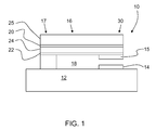
- FIG. 1 shows schematically the basic elements of a known piezoelectric MEMS switch.
- the switch 10 is fabricated onto a base substrate 12.
- the switch includes a pair of contacts, one of which is shown as RF lines 14 on the substrate 12, with shorting bar 15 poised above the RF lines, in the open switch shown.
- the shorting bar 15 is formed on and supported by a cantilever 16.
- the cantilever 16 has one end 17 anchored to the substrate 12, and the larger portion of its structure is suspended and spaced from substrate 12. This separating space 18 contained sacrificial material in the initial fabrication stages.
- the cantilever 16 has a layered structure including a pair of electrode layers 20, 22 between which is sandwiched a piezoelectric layer 24. On top of the cantilever beam a structural layer 25 is present to create a bending moment upon actuation. Bending movement of the cantilever 16 is induced by the actuator formed by electrode layers 20 and 22 and the piezoelectric layer 24 and the structural layer 25.
- the cantilever 16 is flexible and when bending, its outer end 30 can move up and down (reciprocate) while the cantilever is held fixed at opposite end 18. This reciprocation moves the shorting bar 15 down into electrical communication with the RF lines 14.
- the cantilever 16 When not actuated, the cantilever 16 is in the relaxed position, i.e. horizontal position based on the orientation of the figures.
- the cantilever can include one or more through-holes extending to the space 18 below the cantilever from which sacrificial material was removed via the through-hole.
- the space 18 can be over the substrate (as shown) or it may be defined by a region micro machined into the substrate.
- Figure 2 shows a first example of device of the invention.
- the cantilever is designed as a cantilever beam arrangement, in this example with five parallel beams 40,42,44,46,48. In general, three or more cantilever beams are actuated next to each other and connected with each other to achieve a higher contact force at the contacts.
- the multiple cantilevers are connected with each other at their fixed connection ends 50 (fixed with respect to the substrate) and at their free contact ends 52 to define a single shared contact region 54.
- the parallel beams can thus be connected only at their ends, but intermediate connection points can also be provided (preferably less than 10 connection bridges in total, and more preferably only two or three).
- the contact region 54 has (downward facing) contact dimples 56.
- Figure 2 shows the two RF lines 57, 58 which are electrically shortcircuited by the contact region upon actuation of the MEMS switch, i.e. in the second (closed) state.
- the top and bottom actuation electrodes of the cantilever beam arrangement and the piezoelectric layer have essentially the same shape, corresponding to the combined area of the five cantilever beams.
- the contact pad 60 thus comprises a top pad for the top electrode and a bottom pad for the bottom electrode.
- the multiple cantilever beam arrangement enables the gap between the beams to be used as the sacrificial etch holes.
- the sacrificial etch hole pattern is defined by the combination of the strips shown as 62.
- a central beam 48 of the beam arrangement is longer than the other beams, and has the contact region 54 at its free end, the other beams coupling to the central beam at a position set back from free end.
- the contact region 54 can be placed at or near the location where the cantilevers cross/connect. This measure enables the heat conduction to be increased to increase the power handling. Examples are shown in Figures 3 and 4 , in which the same reference numbers denote the same components as in Figure 2 .
- the cantilever beams can have different lengths to remove unwanted deformations and to prevent touching of the substrate other than at the contact region.
- the cantilever beam arrangement is preferably straight (as shown) but it can also be curved, though preferably with a curve less than 90 degrees.
- the under etch process may require additional etch holes. This may be necessary when several cantilever beams are used.
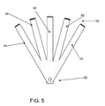
- the cantilever beams are preferably parallel. However, more generally they may be placed next to each other with angle of less than 90 degrees for the complete arrangement. An example is shown in Figure 5 .
- Each beam has a free end 52 and a clamped end 50, so that a double clamped beam geometry is avoided.
- the cantilevers are spaced from each other no more than two times their width (i.e. the space is not more than two times the width of the largest beam on opposite sides of the space- the beams may not have equal width). Preferably they are spaced less than one times the maximum beam width on either side of the spacing.
- cantilever beams can assist to achieve a homogeneous sacrificial layer under etch.
- the designs of the invention avoid the need for stress reducing structures.
- the residual stress in the width direction is relaxed because of the high length to width ratio that can be employed for the individual beams.
- the stiffness in the width direction is very small. Because the cantilevers are clamped only at one end, the residual stress can relax in the length direction. Compensation of the bending moment caused by a residual stress asymmetry in the layer stack can be implemented.
- the increased effective bending stiffness can be accounted for by making the double clamped beam longer or by inserting stress-reducing designs. However, these measures both result in larger lateral size.
- Galvanic contacts situated at or near the tip of a long cantilever suffer from poor heat conduction because of the thin and long geometry of the cantilever. Other heat conduction mechanisms like radiation and convection are negligible because of the low temperature and the small surface area, respectively. This limits the power handling of the galvanic contacts because of the heat generated near the electrical contacts.
- the individual beams at or near the contact region for example each individual beam extends at least 80% of the length of the overall beam configuration, preferably at least 90%
- the heat conduction is increased by several times, nearly linearly with the number of cantilevers. This increases the power handling capabilities of the switch.
- the invention can be implemented without increasing the complexity of the switch fabrication.
- the invention can be implemented by changing the mask design only of existing designs.
- the application is of particular interest for galvanic switches (analog switches, RF switches, high power switches), but is also applicable to other piezoelectric actuators with increased actuation force.
Landscapes
- Micromachines (AREA)
Abstract
A piezoelectric MEMS device, comprises a cantilever beam arrangement (16) with a piezoelectric actuation layer (24) for actuating movement of the cantilever beam arrangement between an open position and a closed position in which the cantilever beam arrangement causes contact with a first electrical contact (15). The cantilever beam arrangement (16) comprises at least three adjacent cantilever beams (40,42,44,46,48), wherein the beams each have a fixed connection end and are coupled together at their free contact ends to define a single shared contact region (54).
The device thus comprises at least three cantilevers actuated next to each other in such a way that all contribute to the contact force. The contact force is thus increased nearly linearly with the number of cantilevers.
Description
- This invention relates to piezoelectric MEMS devices, particularly but not exclusively a MEMS galvanic switch.
- A piezoelectric MEMS galvanic switch comprises a first electrode that is present on a substrate and a movable element that overlies at least partially the first electrode and comprises a piezoelectric actuator. The movable element is movable towards and/or away from the substrate between a first and a second position by application of an actuation voltage to the piezoelectric actuator, in which first position is separated from the substrate by a gap. The movable element comprises a second electrode that faces the first electrode. In the second position (closed switch) first and second electrodes are in mechanical and electrical contact with each other.
- Such an electronic device is for instance known from
GB-A 2,353,410 -
WO 2005/064701 discloses an arrangement in which one of the actuation electrodes of the actuator is simultaneously the second electrode through which contact may be made with the first electrode in the second (closed) position of the MEMS switch. - When a MEMS switch is to function as a galvanic switch (i.e. an open circuit or a closed circuit rather than as a variable capacitance as in capacitive MEMS switches), low contact forces present a problem, especially when applying only a low actuation voltage. If a series switch geometry is used, in which two electrical contacts are needed, the available contact force per contact is also reduced by half.
- For beam like piezoelectric actuators the available contact force increases linearly with the beam width. Hence, a wide beam is desired to achieve high contact forces. However, the piezoelectric beam will not deform only along the length of the beam, as desired, but there will also be unwanted deformations across the beam width. These deformations do not increase the contact force, but instead lead to a decrease of the contact force for a given energy input, because of the (virtual) work needed for the deformation. This is particularly problematic for wider cantilever beams. When the width of a cantilever is increased, the amount of cantilever bending in the width direction increases. This leads to an increased bending stiffness and to a decreased contact force.
- Thus, there is a problem of providing good contact force in the closed switch position, without requiring high voltage actuation signals.
- According to the invention, there is provided a piezoelectric MEMS device, comprising:
- a substrate;
- a first electrical contact over the substrate;
- a cantilever beam arrangement suspended over the substrate, comprising a piezoelectric actuation layer for actuating movement of the cantilever beam arrangement between an open position in which the cantilever beam arrangement is spaced from the first electrical contact and a closed position in which the cantilever beam arrangement causes contact with the first electrical contact, the cantilever beam arrangement comprising a fixed connection end which is fixed with respect to the substrate and a free contact end,
- wherein the cantilever beam arrangement comprises at least three adjacent cantilever beams all extending within an angle of less than 90 degrees, wherein the beams each have a fixed connection end and are coupled together at their free contact ends to define a single shared contact region.
- The device thus comprises at least three cantilevers actuated next to each other in such a way that all contribute to the contact force. The contact force is thus increased nearly linearly with the number of cantilevers. In the most preferable option, between 3 and 5 cantilevers are actuated next to each other.
- In one example with 5 cantilevers, the contact force is increased by a factor of 4.5 of the contact force of a single cantilever. The total number of cantilevers is limited depending on the width, length and thickness of the cantilevers.
- This enables the individual beams to be kept narrow so that bending in the width direction can be substantially avoided. This lateral bending is particularly problematic for wider cantilever beams. When the width of a cantilever is increased, the cantilever starts to bend significantly also in the width direction. For a 200 µm long and 2 µm thick cantilever, this point is at around 30 µm. Thus by using multiple, thin cantilevers the resulting contact force is higher than a comparable single, very wide cantilever. At the same time, the required under etch distance is reduced or the need for etch holes in the cantilevers can be eliminated. Etch holes in the multiple cantilevers might can however still be used if desired.
- The use of relatively narrow cantilevers also means the switching speed is not significantly reduced by squeeze film damping, which will arise for a single, wider cantilever.
- Preferably, the cantilever beam arrangement has less than 9 beams, for example 3, 4 or 5 beams.
- The beams of the cantilever beam arrangement can be parallel. This gives a compact arrangement which is simple to implement. The beams of the cantilever beam arrangement can be spaced by less than two times the width of either beam on opposite sides of the spacing, or more preferably less than the width of either beam on opposite sides of the spacing.
- The beams of the cantilever beam arrangement preferably each have a width of less than 40 µm. The length of each cantilever beam is for example longer than 30 µm and shorter than 1000 µm. Preferably the length is between 50 and 200 µm. The thickness is related to the length of the cantilever beam. Typically, the thickness is a factor of 30 to 200 less than the length of the cantilevers.
- In one arrangement, a central beam of the cantilever beam arrangement is longer than the other beams, and has the contact region at its free end, the other beams coupling to the central beam at a position set back from free end. Thus, one longer beam carries the contact.
- Instead, the width of the cantilever beam arrangement at the location of the contact region can be at least twice the width of a central beam. This gives a greater area for heat dissipation, and means that the beams connect to each other at the very end.
- The actuator can comprise a galvanic MEMS switch, although the invention can be applied to other piezoelectric actuators in order to increase the contact force in the closed configuration.
- These and other aspects of the device of the invention will be further explained with reference to the Figures, in which:
-
Fig. 1 shows in schematic form a cross-sectional view of a known galvanic piezoelectric MEMS switch, and which structure can be used for the device of the invention; -
Fig. 2 shows diagrammatically a plan view a first embodiment of the device of the invention; -
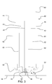
Fig. 3 shows diagrammatically a plan view a second embodiment of the device of the invention; -
Fig. 4 shows diagrammatically a plan view a third embodiment of the device of the invention; and -
Fig. 5 shows diagrammatically a plan view a fourth embodiment of the device of the invention. - The invention provides a galvanic piezoelectric MEMS switch which comprises more than two cantilevers actuated next to each other in such a way that all contribute to the contact force. The contact force is increased nearly linearly with the number of cantilevers. In the most preferable option between 3 and 5 cantilevers are actuated next to each other.
-
Figure 1 shows schematically the basic elements of a known piezoelectric MEMS switch. Theswitch 10 is fabricated onto abase substrate 12. The switch includes a pair of contacts, one of which is shown as RF lines 14 on thesubstrate 12, with shortingbar 15 poised above the RF lines, in the open switch shown. The shortingbar 15 is formed on and supported by acantilever 16. - The
cantilever 16 has oneend 17 anchored to thesubstrate 12, and the larger portion of its structure is suspended and spaced fromsubstrate 12. This separatingspace 18 contained sacrificial material in the initial fabrication stages. - The
cantilever 16 has a layered structure including a pair of electrode layers 20, 22 between which is sandwiched apiezoelectric layer 24. On top of the cantilever beam astructural layer 25 is present to create a bending moment upon actuation. Bending movement of thecantilever 16 is induced by the actuator formed byelectrode layers 20 and 22 and thepiezoelectric layer 24 and thestructural layer 25. Thecantilever 16 is flexible and when bending, itsouter end 30 can move up and down (reciprocate) while the cantilever is held fixed atopposite end 18. This reciprocation moves the shortingbar 15 down into electrical communication with the RF lines 14. - When not actuated, the
cantilever 16 is in the relaxed position, i.e. horizontal position based on the orientation of the figures. The cantilever can include one or more through-holes extending to thespace 18 below the cantilever from which sacrificial material was removed via the through-hole. - The
space 18 can be over the substrate (as shown) or it may be defined by a region micro machined into the substrate. - The design and manufacture of this type of MEMS switch is now extremely well known, and for this reason, details of the processes and materials used will not be given. As will become apparent from the description below, the invention can be implemented simply by changing the plan view layout of the device; no changes to the processes or materials used compared to known MEMS switches are required.
-
Figure 2 shows a first example of device of the invention. - The cantilever is designed as a cantilever beam arrangement, in this example with five
parallel beams - The multiple cantilevers are connected with each other at their fixed connection ends 50 (fixed with respect to the substrate) and at their free contact ends 52 to define a single shared
contact region 54. - The parallel beams can thus be connected only at their ends, but intermediate connection points can also be provided (preferably less than 10 connection bridges in total, and more preferably only two or three).
- The
contact region 54 has (downward facing) contact dimples 56. -
Figure 2 shows the twoRF lines - The top and bottom actuation electrodes of the cantilever beam arrangement and the piezoelectric layer have essentially the same shape, corresponding to the combined area of the five cantilever beams. The
contact pad 60 thus comprises a top pad for the top electrode and a bottom pad for the bottom electrode. - The multiple cantilever beam arrangement enables the gap between the beams to be used as the sacrificial etch holes. The sacrificial etch hole pattern is defined by the combination of the strips shown as 62.
- In the arrangement of
Figure 2 , acentral beam 48 of the beam arrangement is longer than the other beams, and has thecontact region 54 at its free end, the other beams coupling to the central beam at a position set back from free end. - However, the
contact region 54 can be placed at or near the location where the cantilevers cross/connect. This measure enables the heat conduction to be increased to increase the power handling. Examples are shown inFigures 3 and4 , in which the same reference numbers denote the same components as inFigure 2 . - In the example of
Figure 3 , the central threebeams beams - In the example of
Figure 4 , all five beams merge near the contact region. - The cantilever beams can have different lengths to remove unwanted deformations and to prevent touching of the substrate other than at the contact region.
- The cantilever beam arrangement is preferably straight (as shown) but it can also be curved, though preferably with a curve less than 90 degrees.
- The under etch process may require additional etch holes. This may be necessary when several cantilever beams are used.
- The cantilever beams are preferably parallel. However, more generally they may be placed next to each other with angle of less than 90 degrees for the complete arrangement. An example is shown in
Figure 5 . Each beam has afree end 52 and a clampedend 50, so that a double clamped beam geometry is avoided. - For the parallel versions, the cantilevers are spaced from each other no more than two times their width (i.e. the space is not more than two times the width of the largest beam on opposite sides of the space- the beams may not have equal width). Preferably they are spaced less than one times the maximum beam width on either side of the spacing.
- The use of different width cantilever beams can assist to achieve a homogeneous sacrificial layer under etch.
- The designs of the invention avoid the need for stress reducing structures. The residual stress in the width direction is relaxed because of the high length to width ratio that can be employed for the individual beams. The stiffness in the width direction is very small. Because the cantilevers are clamped only at one end, the residual stress can relax in the length direction. Compensation of the bending moment caused by a residual stress asymmetry in the layer stack can be implemented.
- In contrast, in a double-clamped geometry the residual stresses of the layers are compounded. In many cases, these residual stresses are large and usually tensile. This results in an increased effective bending stiffness EIeff of the double clamped beam.

EI is the bending stiffness of the double clamped beam without residual stress
L is the length of the double clamped beam, S the lateral forces (positive force means pulling at the ends of the beam, e.g. created by tensile residual stress)
ti is the thickness, bi the width and σi the residual stress (tensile stress is positive) of the i-th layer of the layer stack. - The increased effective bending stiffness can be accounted for by making the double clamped beam longer or by inserting stress-reducing designs. However, these measures both result in larger lateral size.
- The use of multiple free-clamped beams according to the invention, actuated together, resolves problems of residual stresses without drastically increasing lateral space. Furthermore, the thermal expansion coefficient is more easily controlled than in a double-clamped beam.
- Galvanic contacts situated at or near the tip of a long cantilever suffer from poor heat conduction because of the thin and long geometry of the cantilever. Other heat conduction mechanisms like radiation and convection are negligible because of the low temperature and the small surface area, respectively. This limits the power handling of the galvanic contacts because of the heat generated near the electrical contacts. By attaching the individual beams at or near the contact region (for example each individual beam extends at least 80% of the length of the overall beam configuration, preferably at least 90%), the heat conduction is increased by several times, nearly linearly with the number of cantilevers. This increases the power handling capabilities of the switch.
- The invention can be implemented without increasing the complexity of the switch fabrication. The invention can be implemented by changing the mask design only of existing designs.
- The application is of particular interest for galvanic switches (analog switches, RF switches, high power switches), but is also applicable to other piezoelectric actuators with increased actuation force.
- Various other modifications will be apparent to those skilled in the art.
Claims (10)
- A piezoelectric MEMS device, comprising:a substrate (12);a first electrical contact (14) over the substrate;a cantilever beam arrangement (16) suspended over the substrate, comprising a piezoelectric actuation layer (24) for actuating movement of the cantilever beam arrangement between an open position in which the cantilever beam arrangement (16) is spaced from the first electrical contact (14) and a closed position in which the cantilever beam arrangement causes contact with the first electrical contact (14), the cantilever beam arrangement comprising a fixed connection end (17) which is fixed with respect to the substrate (12) and a free contact end (30),wherein the cantilever beam arrangement (16) comprises at least three adjacent cantilever beams (40,42,44,46,48) all extending within an angle of less than 90 degrees, wherein the beams (40,42,44,46,48) each have a fixed connection end (50) and are coupled together at their free contact ends (52) to define a single shared contact region (54).
- A device as claimed in claim 1, wherein the cantilever beam arrangement (16) has less than 9 beams (40,42,44,46,48).
- A device as claimed in claim 1, wherein the cantilever beam arrangement (16) has 3, 4 or 5 beams (40,42,44,46,48).
- A device as claimed in any preceding claim, wherein the beams (40,42,44,46,48) of the cantilever beam arrangement are parallel.
- A device as claimed in claim 4, wherein the beams (40,42,44,46,48) of the cantilever beam are spaced by less than two times the width of either beam on opposite sides of the spacing.
- A device as claimed in claim 5, wherein the beams (40,42,44,46,48) of the cantilever beam arrangement (16) are spaced by less than the width of either beam on opposite sides of the spacing.
- A device as claimed in any preceding claim, wherein the beams (40,42,44,46,48) of the cantilever beam arrangement (16) each have a width of less than 40 µm.
- A device as claimed in any one of claims 1 to 6, wherein a central beam (48) of the cantilever beam arrangement (16) is longer than the other beams, and has the contact region (54) at its free end, the other beams (40,42,44,46) coupling to the central beam at a position set back from free end (54).
- A device as claimed in any preceding claim, wherein the width of the cantilever beam arrangement (16) at the location of the contact region (54) is at least twice the width of a central beam.
- A device as claimed in any preceding claim, comprising a galvanic MEMS switch.
Priority Applications (1)
| Application Number | Priority Date | Filing Date | Title |
|---|---|---|---|
| EP09174354A EP2317532A1 (en) | 2009-10-28 | 2009-10-28 | Piezoelectric MEMS Device |
Applications Claiming Priority (1)
| Application Number | Priority Date | Filing Date | Title |
|---|---|---|---|
| EP09174354A EP2317532A1 (en) | 2009-10-28 | 2009-10-28 | Piezoelectric MEMS Device |
Publications (1)
| Publication Number | Publication Date |
|---|---|
| EP2317532A1 true EP2317532A1 (en) | 2011-05-04 |
Family
ID=41722969
Family Applications (1)
| Application Number | Title | Priority Date | Filing Date |
|---|---|---|---|
| EP09174354A Withdrawn EP2317532A1 (en) | 2009-10-28 | 2009-10-28 | Piezoelectric MEMS Device |
Country Status (1)
| Country | Link |
|---|---|
| EP (1) | EP2317532A1 (en) |
Cited By (2)
| Publication number | Priority date | Publication date | Assignee | Title |
|---|---|---|---|---|
| US9016133B2 (en) | 2011-01-05 | 2015-04-28 | Nxp, B.V. | Pressure sensor with pressure-actuated switch |
| CN108249388A (en) * | 2016-12-29 | 2018-07-06 | 意法半导体股份有限公司 | The piezoelectric type micro electromechanical actuator equipment that can be moved in the planes |
Citations (3)
| Publication number | Priority date | Publication date | Assignee | Title |
|---|---|---|---|---|
| GB2353410A (en) * | 1999-08-18 | 2001-02-21 | Marconi Electronic Syst Ltd | Electrical switch |
| US20060119227A1 (en) * | 2004-12-08 | 2006-06-08 | Kabushiki Kaisha Toshiba | Piezoelectric driving type MEMS apparatus |
| WO2008075778A1 (en) * | 2006-12-21 | 2008-06-26 | Nikon Corporation | Thin film structure, microactuator, optical shutter device, luminous flux adjusting device and microswitch |
-
2009
- 2009-10-28 EP EP09174354A patent/EP2317532A1/en not_active Withdrawn
Patent Citations (3)
| Publication number | Priority date | Publication date | Assignee | Title |
|---|---|---|---|---|
| GB2353410A (en) * | 1999-08-18 | 2001-02-21 | Marconi Electronic Syst Ltd | Electrical switch |
| US20060119227A1 (en) * | 2004-12-08 | 2006-06-08 | Kabushiki Kaisha Toshiba | Piezoelectric driving type MEMS apparatus |
| WO2008075778A1 (en) * | 2006-12-21 | 2008-06-26 | Nikon Corporation | Thin film structure, microactuator, optical shutter device, luminous flux adjusting device and microswitch |
Cited By (3)
| Publication number | Priority date | Publication date | Assignee | Title |
|---|---|---|---|---|
| US9016133B2 (en) | 2011-01-05 | 2015-04-28 | Nxp, B.V. | Pressure sensor with pressure-actuated switch |
| CN108249388A (en) * | 2016-12-29 | 2018-07-06 | 意法半导体股份有限公司 | The piezoelectric type micro electromechanical actuator equipment that can be moved in the planes |
| CN108249388B (en) * | 2016-12-29 | 2023-08-11 | 意法半导体股份有限公司 | Piezoelectric microelectromechanical actuator device movable in a plane |
Similar Documents
| Publication | Publication Date | Title |
|---|---|---|
| JP4130736B2 (en) | Microdevice with thermal actuator | |
| US6646364B1 (en) | MEMS actuator with lower power consumption and lower cost simplified fabrication | |
| Hosaka et al. | Electromagnetic microrelays: concepts and fundamental characteristics | |
| EP1807856B1 (en) | Spring structure for mems device | |
| US6507138B1 (en) | Very compact, high-stability electrostatic actuator featuring contact-free self-limiting displacement | |
| KR101230284B1 (en) | Rf mems switch a flexible and free switch membrane | |
| CN108333394B (en) | touch probe | |
| JP4580745B2 (en) | Piezoelectric drive MEMS device | |
| US20040124945A1 (en) | Switch | |
| JP3709847B2 (en) | Electrostatic actuator | |
| Yang et al. | Compact, planar, translational piezoelectric bimorph actuator with Archimedes’ spiral actuating tethers | |
| EP2317532A1 (en) | Piezoelectric MEMS Device | |
| Yadav et al. | A two-terminal bistable electrothermally actuated microswitch | |
| US20080182228A1 (en) | Touch Screen Device | |
| TW583701B (en) | A longitudinal piezoelectric optical latching relay | |
| US20070247018A1 (en) | Electrostatic actuation method and electrostatic actuator with integral electrodes for microelectromechanical systems | |
| JP4571488B2 (en) | Fine structure | |
| US20040183402A1 (en) | Switching apparatus, electric field applying method and switching system | |
| EP1850360A1 (en) | Microswitch with a first actuated portion and a second contact portion | |
| US20170141754A1 (en) | Widely tunable cavity filter using low voltage, large out-of-plane actuation mems | |
| Malik et al. | Modeling and designing of RF MEMS switch using ANSYS | |
| US20070103843A1 (en) | Electrostatic mems components permitting a large vertical displacement | |
| JP2011109822A (en) | Electrostatic drive type actuator and variable capacity device | |
| JP2008517777A (en) | Microsystem with deformable bridge | |
| EP2403799B1 (en) | Mems device |
Legal Events
| Date | Code | Title | Description |
|---|---|---|---|
| PUAI | Public reference made under article 153(3) epc to a published international application that has entered the european phase |
Free format text: ORIGINAL CODE: 0009012 |
|
| AK | Designated contracting states |
Kind code of ref document: A1 Designated state(s): AT BE BG CH CY CZ DE DK EE ES FI FR GB GR HR HU IE IS IT LI LT LU LV MC MK MT NL NO PL PT RO SE SI SK SM TR |
|
| AX | Request for extension of the european patent |
Extension state: AL BA RS |
|
| STAA | Information on the status of an ep patent application or granted ep patent |
Free format text: STATUS: THE APPLICATION IS DEEMED TO BE WITHDRAWN |
|
| 18D | Application deemed to be withdrawn |
Effective date: 20111105 |