EP2317444A1 - Flash memory accessing apparatus and an accessing method thereof - Google Patents
Flash memory accessing apparatus and an accessing method thereof Download PDFInfo
- Publication number
- EP2317444A1 EP2317444A1 EP09174151A EP09174151A EP2317444A1 EP 2317444 A1 EP2317444 A1 EP 2317444A1 EP 09174151 A EP09174151 A EP 09174151A EP 09174151 A EP09174151 A EP 09174151A EP 2317444 A1 EP2317444 A1 EP 2317444A1
- Authority
- EP
- European Patent Office
- Prior art keywords
- flash memory
- memory module
- expanding
- main
- module
- Prior art date
- Legal status (The legal status is an assumption and is not a legal conclusion. Google has not performed a legal analysis and makes no representation as to the accuracy of the status listed.)
- Granted
Links
Images


Classifications
-
- G—PHYSICS
- G06—COMPUTING OR CALCULATING; COUNTING
- G06F—ELECTRIC DIGITAL DATA PROCESSING
- G06F13/00—Interconnection of, or transfer of information or other signals between, memories, input/output devices or central processing units
- G06F13/14—Handling requests for interconnection or transfer
- G06F13/16—Handling requests for interconnection or transfer for access to memory bus
- G06F13/1668—Details of memory controller
- G06F13/1684—Details of memory controller using multiple buses
Definitions
- the present invention relates to a flash memory accessing apparatus and an accessing method thereof. More particularly, the present invention relates to an accessing apparatus for expanding an open NAND flash interface, and an accessing method thereof.
- NAND flash memories are manufactured by many suppliers. Though the NAND flash memories manufactured by different suppliers may have similar packages, input/output pins and similar control command sets, each time when the NAND flash memories manufactured by different suppliers are replaced, firmware adjustments are necessary.
- ONFI open NAND flash interface
- the present invention is directed to a flash memory accessing apparatus and an accessing method thereof, which are used for expanding a flash memory on an open NAND flash interface (ONFI).
- ONFI open NAND flash interface
- the present invention provides a flash memory accessing apparatus including a memory controller, a first ONFI and an expanding flash memory module.
- the first ONFI is coupled to the memory controller, and is used for connecting a main flash memory module.
- the expanding flash memory module is coupled to the memory controller and the first ONFI.
- the memory controller obtains a detecting result by detecting whether the main flash memory module connected to the first ONFI and the expanding flash memory module are single side or double side.
- the memory controller further configures an accessing method of the main flash memory module and the expanding flash memory module according to the detecting result.
- the memory controller when the memory controller detects that the main flash memory module and the expanding flash memory module are all single side, the memory controller connects the main flash memory module and the expanding flash memory module to form a dual channel flash memory module.
- the memory controller when the memory controller detects that the main flash memory module and the expanding flash memory module are all double side, the memory controller configures one of the main flash memory module and the expanding flash memory module as a working memory, and configures another one of the main flash memory module and the expanding flash memory module as a spare memory.
- the memory controller further disables the spare memory.
- the memory controller further detects whether a read or a write operation of the working memory is normal.
- the memory controller when the memory controller detects that the read or the write operation of the working memory is abnormal, the memory controller disables the working memory, and switches the spare memory to serve as the working memory.
- the memory controller, the first ONFI and an expanding flash memory interface are all disposed on a motherboard.
- the flash memory accessing apparatus further includes an expanding flash memory interface.
- the expanding flash memory interface is coupled to the memory controller and the first ONFI, and is used for connecting the expanding flash memory module.
- the memory controller, the first ONFI and the expanding flash memory interface are disposed on a motherboard, and the expanding flash memory interface is a second ONFI.
- the expanding flash memory module is directly disposed on a motherboard, and the memory controller and the first ONFI are disposed on the motherboard.
- the present invention provides a flash memory accessing method. First, a first ONFI is provided to connect a main flash memory module, and an expanding flash memory module is provided. Next, whether the main flash memory module connected to the first ONFI and the expanding flash memory module are single side or double side is detected to obtain a detecting result. Next, an accessing method of the main flash memory module and the expanding flash memory module is configured according to the detecting result.
- the expanding flash memory interface is further provided to expand a capacity of the flash memory, and by detecting a single/double side state of the main flash memory module on the ONFI and the expanding flash memory module on the expanding flash memory interface, the accessing method of the main flash memory module and the expanding flash memory module is configured. Therefore, application of the expanding flash memory module and the main flash memory module is effectively optimized.
- FIG. 1A is a schematic diagram illustrating a flash memory accessing apparatus 100 according to an embodiment of the present invention.
- FIG. 1B and FIG. 1C are schematic diagrams illustrating different approaches of configuring a flash memory accessing apparatus 100 on a motherboard according to an embodiment of the present invention.
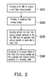
- FIG. 2 is a flowchart illustrating a flash memory accessing method according to an embodiment of the present invention.
- FIG. 1A is a schematic diagram illustrating a flash memory accessing apparatus 100 according to an embodiment of the present invention.
- the flash memory accessing apparatus 100 includes a memory controller 110, an open NAND flash interface (ONFI) 120 and an expanding flash memory interface 130.
- the ONFI 120 is coupled to the memory controller 110, and is used for connecting a main flash memory module 121.
- the expanding flash memory interface 130 is also coupled to the memory controller 110, and is used for connecting an expanding flash memory module 131.
- the memory controller 110 After the main flash memory module 121 is connected to the ONFI 120 and the expanding flash memory module 131 is connected to the expanding flash memory interface 130, the memory controller 110 detects whether the main flash memory module 121 and the expanding flash memory module 131 respectively connected to the ONFI 120 and the expanding flash memory interface 130 are single side memory modules or double side memory modules to obtain a detecting result.
- the memory controller 110 connects the main flash memory module 121 and the expanding flash memory module 131 to form a so-called dual channel flash memory module.
- the memory controller 110 divides data to be stored into two parts, and simultaneously stores the divided two parts into the main flash memory module 121 and the expanding flash memory module 131, respectively, which can effectively increase a data storing speed.
- the memory controller 110 configures one of the main flash memory module 121 and the expanding flash memory module 131 as a working memory, and configures another one of the main flash memory module 121 and the expanding flash memory module 131 as a spare memory. Namely, when the main flash memory module 121 and the expanding flash memory module 131 are all the double side memory modules, only one of the memories can be accessed (the one configured as the working memory), and the other one of the memories is configured as the spare memory and cannot be accessed.
- the memory controller 110 configures the main flash memory module 121 as the working memory for accessing, and configures the expanding flash memory module 131 as the spare memory, and disables the spare memory (the expanding flash memory module 131).
- the memory controller 110 further performs a read/write test on the flash memory module used as the working memory, so as to detect whether the flash memory module used as the working memory is damaged.
- the read/write test performed on the flash memory module used as the working memory for example, the main flash memory module 121 cannot be normally executed, it represents that the main flash memory module 121 is damaged.
- the memory controller 110 switches the expanding flash memory module 131 originally used as the spare memory to the working memory, and disables the main flash memory module 121 originally used as the working memory.
- the memory controller 110 can perform the read/write test to the working memory according to a fixed time period. Namely, the memory controller 110 performs the read/write test on the working memory to detect whether the flash memory module used as the working memory is damaged every the fixed time period.
- the memory controller 110 can further configure the expanding flash memory module 131 to serve as a spare memory of the main flash memory module 121. Namely, besides storing data to the main flash memory module 121, the data can also be stored in the expanding flash memory module 131 as a backup.
- a method to backup the data in the main flash memory module 121 is that the memory controller 110 copies the data in the main flash memory module 121 to the expanding flash memory module 131 every a fixed time period. Calculation of the fixed time period can be implemented by hardware or software.
- the flash memory accessing apparatus 100 can provide a software interface for a user to set or change the fixed time period.
- the memory controller 110, the ONFI 120 and the expanding flash memory interface 130 can be simultaneously disposed on a same circuit substrate (for example, a motherboard).
- the expanding flash memory interface 130 is not used, and the expanding flash memory module 131 is directly disposed on the motherboard.
- FIG. 1B and FIG. 1C for methods of disposing the flash memory accessing apparatus 100 on the motherboard.
- the memory controller 110, the ONFI 120 and the expanding flash memory interface 130 are all disposed on the motherboard 150.
- the main flash memory module 121 is connected to the motherboard 150 through the ONFI 120, and the expanding flash memory module 131 is connected to the motherboard 150 through the expanding flash memory interface 130.
- the memory controller 110 and the ONFI 120 are disposed on the motherboard 150, while the expanding flash memory interface 130 shown in FIG. 1B is not disposed on the motherboard 150.
- the expanding flash memory module 131 is directly disposed on the motherboard 150, which forms a so-called onboard flash memory module.
- FIG. 2 is a flowchart illustrating a flash memory accessing method according to an embodiment of the present invention.
- the method includes following steps. First, a first ONFI is provided to connect a main flash memory module (step S210), and an expanding flash memory module is provided (S220). Next, after the main flash memory module and the expanding flash memory module are connected, it is detected whether the main flash memory module connected to the first ONFI and the expanding flash memory module are single side or double side, so as to obtain a detecting result (S230). Next, an accessing method of the main flash memory module and the expanding flash memory module is configured according to the detecting result (S240).
- obtaining of the detecting result and configuration of the accessing method of the main flash memory module and the expanding flash memory module can all be implemented by a memory controller.
- Implementation of the memory controller is the same to the above described memory controller 110 in the flash memory accessing apparatus 100, and therefore detailed descriptions thereof are not repeated.
- the accessing method of the main flash memory module and the expanding flash memory module can be configured by detecting whether the main flash memory module and the expanding flash memory module are single side or double side. Therefore, a memory volume of the ONFI is effectively expanded, and the main flash memory module and the expanding flash memory module can be efficiently used, so that an accessing bandwidth can be increased, and backup of stored data is achieved.
Landscapes
- Engineering & Computer Science (AREA)
- Theoretical Computer Science (AREA)
- Physics & Mathematics (AREA)
- General Engineering & Computer Science (AREA)
- General Physics & Mathematics (AREA)
- Techniques For Improving Reliability Of Storages (AREA)
Abstract
Description
- BACKGROUND OF THE INVENTION
- 1. Field of the Invention
- The present invention relates to a flash memory accessing apparatus and an accessing method thereof. More particularly, the present invention relates to an accessing apparatus for expanding an open NAND flash interface, and an accessing method thereof.
- 2. Description of Related Art
- In the past, NAND flash memories are manufactured by many suppliers. Though the NAND flash memories manufactured by different suppliers may have similar packages, input/output pins and similar control command sets, each time when the NAND flash memories manufactured by different suppliers are replaced, firmware adjustments are necessary.
- Accordingly, some major suppliers jointly put forward a so-called open NAND flash interface (which is referred to as ONFI hereinafter) standard for providing a standard specification and interface for the NAND flash memory. However, according to the ONFI standard, a controller of the flash memory only provides one set of ONFI signal line. Therefore, if two sets of flash memories are used, the ONFI signal line of the controller of the flash memory has to be dissembled into two sets for utilization, which may cause a great limitation in utilization.
- SUMMARY OF THE INVENTION
- The present invention is directed to a flash memory accessing apparatus and an accessing method thereof, which are used for expanding a flash memory on an open NAND flash interface (ONFI).
- The present invention provides a flash memory accessing apparatus including a memory controller, a first ONFI and an expanding flash memory module. The first ONFI is coupled to the memory controller, and is used for connecting a main flash memory module. The expanding flash memory module is coupled to the memory controller and the first ONFI. Wherein, the memory controller obtains a detecting result by detecting whether the main flash memory module connected to the first ONFI and the expanding flash memory module are single side or double side. The memory controller further configures an accessing method of the main flash memory module and the expanding flash memory module according to the detecting result.
- In an embodiment of the present invention, when the memory controller detects that the main flash memory module and the expanding flash memory module are all single side, the memory controller connects the main flash memory module and the expanding flash memory module to form a dual channel flash memory module.
- In an embodiment of the present invention, when the memory controller detects that the main flash memory module and the expanding flash memory module are all double side, the memory controller configures one of the main flash memory module and the expanding flash memory module as a working memory, and configures another one of the main flash memory module and the expanding flash memory module as a spare memory.
- In an embodiment of the present invention, the memory controller further disables the spare memory.
- In an embodiment of the present invention, the memory controller further detects whether a read or a write operation of the working memory is normal.
- In an embodiment of the present invention, when the memory controller detects that the read or the write operation of the working memory is abnormal, the memory controller disables the working memory, and switches the spare memory to serve as the working memory.
- In an embodiment of the present invention, the memory controller, the first ONFI and an expanding flash memory interface are all disposed on a motherboard.
- In an embodiment of the present invention, the flash memory accessing apparatus further includes an expanding flash memory interface. The expanding flash memory interface is coupled to the memory controller and the first ONFI, and is used for connecting the expanding flash memory module.
- In an embodiment of the present invention, the memory controller, the first ONFI and the expanding flash memory interface are disposed on a motherboard, and the expanding flash memory interface is a second ONFI.
- In an embodiment of the present invention, the expanding flash memory module is directly disposed on a motherboard, and the memory controller and the first ONFI are disposed on the motherboard.
- The present invention provides a flash memory accessing method. First, a first ONFI is provided to connect a main flash memory module, and an expanding flash memory module is provided. Next, whether the main flash memory module connected to the first ONFI and the expanding flash memory module are single side or double side is detected to obtain a detecting result. Next, an accessing method of the main flash memory module and the expanding flash memory module is configured according to the detecting result.
- In the present invention, besides the ONFI, the expanding flash memory interface is further provided to expand a capacity of the flash memory, and by detecting a single/double side state of the main flash memory module on the ONFI and the expanding flash memory module on the expanding flash memory interface, the accessing method of the main flash memory module and the expanding flash memory module is configured. Therefore, application of the expanding flash memory module and the main flash memory module is effectively optimized.
- In order to make the aforementioned and other features and advantages of the present invention comprehensible, several exemplary embodiments accompanied with figures are described in detail below.
- BRIEF DESCRIPTION OF THE DRAWINGS
- The accompanying drawings are included to provide a further understanding of the invention, and are incorporated in and constitute a part of this specification. The drawings illustrate embodiments of the invention and, together with the description, serve to explain the principles of the invention.
-
FIG. 1A is a schematic diagram illustrating a flashmemory accessing apparatus 100 according to an embodiment of the present invention. -
FIG. 1B andFIG. 1C are schematic diagrams illustrating different approaches of configuring a flashmemory accessing apparatus 100 on a motherboard according to an embodiment of the present invention. -
FIG. 2 is a flowchart illustrating a flash memory accessing method according to an embodiment of the present invention. - DESCRIPTION OF THE EMBODIMENTS
- Referring to
FIG. 1A, FIG. 1A is a schematic diagram illustrating a flashmemory accessing apparatus 100 according to an embodiment of the present invention. The flashmemory accessing apparatus 100 includes amemory controller 110, an open NAND flash interface (ONFI) 120 and an expandingflash memory interface 130. TheONFI 120 is coupled to thememory controller 110, and is used for connecting a mainflash memory module 121. The expandingflash memory interface 130 is also coupled to thememory controller 110, and is used for connecting an expandingflash memory module 131. - After the main
flash memory module 121 is connected to theONFI 120 and the expandingflash memory module 131 is connected to the expandingflash memory interface 130, thememory controller 110 detects whether the mainflash memory module 121 and the expandingflash memory module 131 respectively connected to theONFI 120 and the expandingflash memory interface 130 are single side memory modules or double side memory modules to obtain a detecting result. - When the detecting result obtained by the
memory controller 110 indicates that the mainflash memory module 121 and the expandingflash memory module 131 are all the single side memory modules, it represent that a control signal line provided by thememory controller 110 is enough to simultaneously access the mainflash memory module 121 and the expandingflash memory module 131. Therefore, thememory controller 110 connects the mainflash memory module 121 and the expandingflash memory module 131 to form a so-called dual channel flash memory module. In case of the dual channel flash memory module, thememory controller 110 divides data to be stored into two parts, and simultaneously stores the divided two parts into the mainflash memory module 121 and the expandingflash memory module 131, respectively, which can effectively increase a data storing speed. Comparatively, when data is read, two parts of data can be simultaneously read from the mainflash memory module 121 and the expandingflash memory module 131, and thememory controller 110 combines the two parts of data to obtain an original stored data. Similarly, a data reading speed is increased. - Moreover, when the detecting result obtained by the
memory controller 110 indicates that the mainflash memory module 121 and the expandingflash memory module 131 are all the double side memory modules, thememory controller 110 configures one of the mainflash memory module 121 and the expandingflash memory module 131 as a working memory, and configures another one of the mainflash memory module 121 and the expandingflash memory module 131 as a spare memory. Namely, when the mainflash memory module 121 and the expandingflash memory module 131 are all the double side memory modules, only one of the memories can be accessed (the one configured as the working memory), and the other one of the memories is configured as the spare memory and cannot be accessed. - For example, when the detecting result obtained by the
memory controller 110 indicates that the mainflash memory module 121 and the expandingflash memory module 131 are all the double side memory modules, thememory controller 110 configures the mainflash memory module 121 as the working memory for accessing, and configures the expandingflash memory module 131 as the spare memory, and disables the spare memory (the expanding flash memory module 131). - Moreover, the
memory controller 110 further performs a read/write test on the flash memory module used as the working memory, so as to detect whether the flash memory module used as the working memory is damaged. When the read/write test performed on the flash memory module used as the working memory (for example, the main flash memory module 121) cannot be normally executed, it represents that the mainflash memory module 121 is damaged. Then, thememory controller 110 switches the expandingflash memory module 131 originally used as the spare memory to the working memory, and disables the mainflash memory module 121 originally used as the working memory. - The
memory controller 110 can perform the read/write test to the working memory according to a fixed time period. Namely, thememory controller 110 performs the read/write test on the working memory to detect whether the flash memory module used as the working memory is damaged every the fixed time period. - On the other hand, the
memory controller 110 can further configure the expandingflash memory module 131 to serve as a spare memory of the mainflash memory module 121. Namely, besides storing data to the mainflash memory module 121, the data can also be stored in the expandingflash memory module 131 as a backup. A method to backup the data in the mainflash memory module 121 is that thememory controller 110 copies the data in the mainflash memory module 121 to the expandingflash memory module 131 every a fixed time period. Calculation of the fixed time period can be implemented by hardware or software. Moreover, the flashmemory accessing apparatus 100 can provide a software interface for a user to set or change the fixed time period. - It should be noticed that the
memory controller 110, theONFI 120 and the expandingflash memory interface 130 can be simultaneously disposed on a same circuit substrate (for example, a motherboard). Alternatively, the expandingflash memory interface 130 is not used, and the expandingflash memory module 131 is directly disposed on the motherboard. - Referring to
FIG. 1B andFIG. 1C for methods of disposing the flashmemory accessing apparatus 100 on the motherboard. InFIG. 1B , thememory controller 110, theONFI 120 and the expandingflash memory interface 130 are all disposed on themotherboard 150. The mainflash memory module 121 is connected to themotherboard 150 through theONFI 120, and the expandingflash memory module 131 is connected to themotherboard 150 through the expandingflash memory interface 130. - Moreover, in
FIG. 1C , thememory controller 110 and theONFI 120 are disposed on themotherboard 150, while the expandingflash memory interface 130 shown inFIG. 1B is not disposed on themotherboard 150. Comparatively, the expandingflash memory module 131 is directly disposed on themotherboard 150, which forms a so-called onboard flash memory module. - Referring to
FIG. 2, FIG. 2 is a flowchart illustrating a flash memory accessing method according to an embodiment of the present invention. The method includes following steps. First, a first ONFI is provided to connect a main flash memory module (step S210), and an expanding flash memory module is provided (S220). Next, after the main flash memory module and the expanding flash memory module are connected, it is detected whether the main flash memory module connected to the first ONFI and the expanding flash memory module are single side or double side, so as to obtain a detecting result (S230). Next, an accessing method of the main flash memory module and the expanding flash memory module is configured according to the detecting result (S240). - It should be noticed that obtaining of the detecting result and configuration of the accessing method of the main flash memory module and the expanding flash memory module can all be implemented by a memory controller. Implementation of the memory controller is the same to the above described
memory controller 110 in the flashmemory accessing apparatus 100, and therefore detailed descriptions thereof are not repeated. - In summary, in the present invention, the accessing method of the main flash memory module and the expanding flash memory module can be configured by detecting whether the main flash memory module and the expanding flash memory module are single side or double side. Therefore, a memory volume of the ONFI is effectively expanded, and the main flash memory module and the expanding flash memory module can be efficiently used, so that an accessing bandwidth can be increased, and backup of stored data is achieved.
- It will be apparent to those skilled in the art that various modifications and variations can be made to the structure of the present invention without departing from the scope or spirit of the invention. In view of the foregoing, it is intended that the present invention cover modifications and variations of this invention provided they fall within the scope of the following claims and their equivalents.
Claims (16)
- A flash memory accessing apparatus, comprising: a memory controller; a first open NAND flash interface (ONFI), coupled to the memory controller for connecting a main flash memory module; and an expanding flash memory module, coupled to the memory controller and the first ONFI, wherein the memory controller obtains a detecting result by detecting whether the main flash memory module connected to the first ONFI and the expanding flash memory module are single side or double side, and configures an accessing method of the main flash memory module and the expanding flash memory module according to the detecting result.
- The flash memory accessing apparatus as claimed in claim 1, wherein when the memory controller detects that the main flash memory module and the expanding flash memory module are all single side, the memory controller connects the main flash memory module and the expanding flash memory module to form a dual channel flash memory module.
- The flash memory accessing apparatus as claimed in claim 1, wherein when the memory controller detects that the main flash memory module and the expanding flash memory module are all double side, the memory controller configures one of the main flash memory module and the expanding flash memory module as a working memory, and configures another one of the main flash memory module and the expanding flash memory module as a spare memory.
- The flash memory accessing apparatus as claimed in claim 3, wherein the memory controller further disables the spare memory.
- The flash memory accessing apparatus as claimed in claim 3, wherein the memory controller further detects whether a read or a write operation of the working memory is normal.
- The flash memory accessing apparatus as claimed in claim 3, wherein when the memory controller detects that the read or the write operation of the working memory is abnormal, the memory controller disables the working memory, and switches the spare memory to serve as the working memory.
- The flash memory accessing apparatus as claimed in claim 1, further comprising: an expanding flash memory interface, coupled to the memory controller and the first ONFI for connecting the expanding flash memory module.
- The flash memory accessing apparatus as claimed in claim 7, wherein the memory controller, the first ONFI and the expanding flash memory interface are disposed on a motherboard, and the expanding flash memory interface is a second ONFI.
- The flash memory accessing apparatus as claimed in claim 1, wherein the expanding flash memory module is directly disposed on a motherboard, and the memory controller and the first ONFI are disposed on the motherboard.
- A flash memory accessing method, comprising: providing a first ONFI to connect a main flash memory module; providing an expanding flash memory module; providing a memory controller for detecting whether the main flash memory module connected to the first ONFI and the expanding flash memory module are single side or double side to obtain a detecting result; and providing a memory controller for configuring an accessing method of the main flash memory module and the expanding flash memory module according to the detecting result.
- The flash memory accessing method as claimed in claim 10, wherein the detecting result comprises: the main flash memory module and the expanding flash memory module are all single side or the main flash memory module and the expanding flash memory module are all double side.
- The flash memory accessing method as claimed in claim 11, wherein the step of configuring the accessing method of the main flash memory module and the expanding flash memory module according to the detecting result comprises: when the detecting result is that the main flash memory module and the expanding flash memory module are all single side, a memory controller connects the main flash memory module and the expanding flash memory module to form a dual channel flash memory module.
- The flash memory accessing method as claimed in claim 12, wherein the step of configuring the accessing method of the main flash memory module and the expanding flash memory module according to the detecting result further comprises: when the detecting result is that the main flash memory module and the expanding flash memory module are all double side, the memory controller configures one of the main flash memory module and the expanding flash memory module as a working memory, and configures another one of the main flash memory module and the expanding flash memory module as a spare memory.
- The flash memory accessing method as claimed in claim 13, further comprising: providing a memory controller for detecting whether a read or a write operation of the working memory is normal.
- The flash memory accessing method as claimed in claim 14, further comprising: providing a memory controller for disabling the working memory, and switching the spare memory to serve as the working memory by the memory controller when the memory controller detects that the read or the write operation of the working memory is abnormal.
- The flash memory accessing method as claimed in claim 10, further comprising: providing an expanding flash memory interface to connect the expanding flash memory module.
Priority Applications (1)
| Application Number | Priority Date | Filing Date | Title |
|---|---|---|---|
| EP20090174151 EP2317444B1 (en) | 2009-10-27 | 2009-10-27 | Flash memory accessing apparatus and an accessing method thereof |
Applications Claiming Priority (1)
| Application Number | Priority Date | Filing Date | Title |
|---|---|---|---|
| EP20090174151 EP2317444B1 (en) | 2009-10-27 | 2009-10-27 | Flash memory accessing apparatus and an accessing method thereof |
Publications (2)
| Publication Number | Publication Date |
|---|---|
| EP2317444A1 true EP2317444A1 (en) | 2011-05-04 |
| EP2317444B1 EP2317444B1 (en) | 2012-08-15 |
Family
ID=42029885
Family Applications (1)
| Application Number | Title | Priority Date | Filing Date |
|---|---|---|---|
| EP20090174151 Not-in-force EP2317444B1 (en) | 2009-10-27 | 2009-10-27 | Flash memory accessing apparatus and an accessing method thereof |
Country Status (1)
| Country | Link |
|---|---|
| EP (1) | EP2317444B1 (en) |
Cited By (1)
| Publication number | Priority date | Publication date | Assignee | Title |
|---|---|---|---|---|
| KR20170058699A (en) * | 2015-11-19 | 2017-05-29 | 삼성전자주식회사 | Non-volatile memory module and electronic device having the same |
Citations (1)
| Publication number | Priority date | Publication date | Assignee | Title |
|---|---|---|---|---|
| US20090164703A1 (en) * | 2007-12-21 | 2009-06-25 | Spansion Llc | Flexible flash interface |
-
2009
- 2009-10-27 EP EP20090174151 patent/EP2317444B1/en not_active Not-in-force
Patent Citations (1)
| Publication number | Priority date | Publication date | Assignee | Title |
|---|---|---|---|---|
| US20090164703A1 (en) * | 2007-12-21 | 2009-06-25 | Spansion Llc | Flexible flash interface |
Non-Patent Citations (1)
| Title |
|---|
| ONFI WORKGROUP: "Open NAND Flash Interface Specification, Revision 2.2", 7 October 2009 (2009-10-07), XP002576107, Retrieved from the Internet <URL:www.onfi.org> [retrieved on 20100326] * |
Cited By (1)
| Publication number | Priority date | Publication date | Assignee | Title |
|---|---|---|---|---|
| KR20170058699A (en) * | 2015-11-19 | 2017-05-29 | 삼성전자주식회사 | Non-volatile memory module and electronic device having the same |
Also Published As
| Publication number | Publication date |
|---|---|
| EP2317444B1 (en) | 2012-08-15 |
Similar Documents
| Publication | Publication Date | Title |
|---|---|---|
| US8205038B2 (en) | Flash memory accessing apparatus and accessing method thereof | |
| KR101652874B1 (en) | On chip redundancy repair for memory devices | |
| US11693802B2 (en) | NAND switch | |
| KR101149270B1 (en) | Systems and methods for testing integrated circuit devices | |
| TWI386852B (en) | System for switching bios and method thereof | |
| CN102135927B (en) | Method and device for system booting based on NAND FLASH | |
| US10802750B2 (en) | Universal flash storage memory module, controller and electronic device with advanced turbo write buffer and method for operating the memory module | |
| CN102906710B (en) | A kind of Bootrom backup method and device | |
| US7856614B2 (en) | Programmable system-on-chip apparatus and method for updating firmware | |
| CN103247345A (en) | Quick-flash memory and detection method for failure memory cell of quick-flash memory | |
| CN103208314A (en) | Memory testing method of embedded system and embedded system | |
| CN116597887B (en) | Capacity reduction test method, system and equipment for LPDDR chip and storage medium | |
| EP2317444B1 (en) | Flash memory accessing apparatus and an accessing method thereof | |
| US9058863B2 (en) | Reference frequency setting method, memory controller and memory storage apparatus | |
| KR101295413B1 (en) | Device and method for testing of nand type flash memory | |
| CN106030544A (en) | Random access memory detection method of computer device and computer device | |
| CN110874333A (en) | Storage device and storage method | |
| CN116504292B (en) | Method and device for reading non flash, memory chip and equipment | |
| CN103902301A (en) | Method and device and processor reading BIOS | |
| JP5027198B2 (en) | Flash memory access device and access method | |
| US20170199693A1 (en) | Electronic system having power-condition-aware hybrid storage device and method for operation of hybrid storage device in electronic system | |
| CN104134464A (en) | System and method for testing address line | |
| CN102054521B (en) | Access device and access method for flash memory | |
| CN101739261B (en) | Switching system and switching method of basic input and output system | |
| TWI430272B (en) | Flash memory accessing apparatius and accessing method thereof |
Legal Events
| Date | Code | Title | Description |
|---|---|---|---|
| PUAI | Public reference made under article 153(3) epc to a published international application that has entered the european phase |
Free format text: ORIGINAL CODE: 0009012 |
|
| AK | Designated contracting states |
Kind code of ref document: A1 Designated state(s): AT BE BG CH CY CZ DE DK EE ES FI FR GB GR HR HU IE IS IT LI LT LU LV MC MK MT NL NO PL PT RO SE SI SK SM TR |
|
| AX | Request for extension of the european patent |
Extension state: AL BA RS |
|
| 17P | Request for examination filed |
Effective date: 20111031 |
|
| GRAP | Despatch of communication of intention to grant a patent |
Free format text: ORIGINAL CODE: EPIDOSNIGR1 |
|
| GRAC | Information related to communication of intention to grant a patent modified |
Free format text: ORIGINAL CODE: EPIDOSCIGR1 |
|
| GRAS | Grant fee paid |
Free format text: ORIGINAL CODE: EPIDOSNIGR3 |
|
| GRAA | (expected) grant |
Free format text: ORIGINAL CODE: 0009210 |
|
| AK | Designated contracting states |
Kind code of ref document: B1 Designated state(s): AT BE BG CH CY CZ DE DK EE ES FI FR GB GR HR HU IE IS IT LI LT LU LV MC MK MT NL NO PL PT RO SE SI SK SM TR |
|
| REG | Reference to a national code |
Ref country code: AT Ref legal event code: REF Ref document number: 571149 Country of ref document: AT Kind code of ref document: T Effective date: 20120815 Ref country code: GB Ref legal event code: FG4D Ref country code: CH Ref legal event code: EP |
|
| REG | Reference to a national code |
Ref country code: IE Ref legal event code: FG4D |
|
| REG | Reference to a national code |
Ref country code: NL Ref legal event code: T3 |
|
| REG | Reference to a national code |
Ref country code: DE Ref legal event code: R096 Ref document number: 602009008950 Country of ref document: DE Effective date: 20121018 |
|
| REG | Reference to a national code |
Ref country code: AT Ref legal event code: MK05 Ref document number: 571149 Country of ref document: AT Kind code of ref document: T Effective date: 20120815 |
|
| PG25 | Lapsed in a contracting state [announced via postgrant information from national office to epo] |
Ref country code: IS Free format text: LAPSE BECAUSE OF FAILURE TO SUBMIT A TRANSLATION OF THE DESCRIPTION OR TO PAY THE FEE WITHIN THE PRESCRIBED TIME-LIMIT Effective date: 20121215 Ref country code: NO Free format text: LAPSE BECAUSE OF FAILURE TO SUBMIT A TRANSLATION OF THE DESCRIPTION OR TO PAY THE FEE WITHIN THE PRESCRIBED TIME-LIMIT Effective date: 20121115 Ref country code: LT Free format text: LAPSE BECAUSE OF FAILURE TO SUBMIT A TRANSLATION OF THE DESCRIPTION OR TO PAY THE FEE WITHIN THE PRESCRIBED TIME-LIMIT Effective date: 20120815 Ref country code: FI Free format text: LAPSE BECAUSE OF FAILURE TO SUBMIT A TRANSLATION OF THE DESCRIPTION OR TO PAY THE FEE WITHIN THE PRESCRIBED TIME-LIMIT Effective date: 20120815 Ref country code: HR Free format text: LAPSE BECAUSE OF FAILURE TO SUBMIT A TRANSLATION OF THE DESCRIPTION OR TO PAY THE FEE WITHIN THE PRESCRIBED TIME-LIMIT Effective date: 20120815 Ref country code: AT Free format text: LAPSE BECAUSE OF FAILURE TO SUBMIT A TRANSLATION OF THE DESCRIPTION OR TO PAY THE FEE WITHIN THE PRESCRIBED TIME-LIMIT Effective date: 20120815 |
|
| PG25 | Lapsed in a contracting state [announced via postgrant information from national office to epo] |
Ref country code: PT Free format text: LAPSE BECAUSE OF FAILURE TO SUBMIT A TRANSLATION OF THE DESCRIPTION OR TO PAY THE FEE WITHIN THE PRESCRIBED TIME-LIMIT Effective date: 20121217 Ref country code: SI Free format text: LAPSE BECAUSE OF FAILURE TO SUBMIT A TRANSLATION OF THE DESCRIPTION OR TO PAY THE FEE WITHIN THE PRESCRIBED TIME-LIMIT Effective date: 20120815 Ref country code: SE Free format text: LAPSE BECAUSE OF FAILURE TO SUBMIT A TRANSLATION OF THE DESCRIPTION OR TO PAY THE FEE WITHIN THE PRESCRIBED TIME-LIMIT Effective date: 20120815 Ref country code: BE Free format text: LAPSE BECAUSE OF FAILURE TO SUBMIT A TRANSLATION OF THE DESCRIPTION OR TO PAY THE FEE WITHIN THE PRESCRIBED TIME-LIMIT Effective date: 20120815 Ref country code: LV Free format text: LAPSE BECAUSE OF FAILURE TO SUBMIT A TRANSLATION OF THE DESCRIPTION OR TO PAY THE FEE WITHIN THE PRESCRIBED TIME-LIMIT Effective date: 20120815 Ref country code: PL Free format text: LAPSE BECAUSE OF FAILURE TO SUBMIT A TRANSLATION OF THE DESCRIPTION OR TO PAY THE FEE WITHIN THE PRESCRIBED TIME-LIMIT Effective date: 20120815 Ref country code: GR Free format text: LAPSE BECAUSE OF FAILURE TO SUBMIT A TRANSLATION OF THE DESCRIPTION OR TO PAY THE FEE WITHIN THE PRESCRIBED TIME-LIMIT Effective date: 20121116 |
|
| PG25 | Lapsed in a contracting state [announced via postgrant information from national office to epo] |
Ref country code: EE Free format text: LAPSE BECAUSE OF FAILURE TO SUBMIT A TRANSLATION OF THE DESCRIPTION OR TO PAY THE FEE WITHIN THE PRESCRIBED TIME-LIMIT Effective date: 20120815 Ref country code: ES Free format text: LAPSE BECAUSE OF FAILURE TO SUBMIT A TRANSLATION OF THE DESCRIPTION OR TO PAY THE FEE WITHIN THE PRESCRIBED TIME-LIMIT Effective date: 20121126 Ref country code: DK Free format text: LAPSE BECAUSE OF FAILURE TO SUBMIT A TRANSLATION OF THE DESCRIPTION OR TO PAY THE FEE WITHIN THE PRESCRIBED TIME-LIMIT Effective date: 20120815 Ref country code: RO Free format text: LAPSE BECAUSE OF FAILURE TO SUBMIT A TRANSLATION OF THE DESCRIPTION OR TO PAY THE FEE WITHIN THE PRESCRIBED TIME-LIMIT Effective date: 20120815 Ref country code: CZ Free format text: LAPSE BECAUSE OF FAILURE TO SUBMIT A TRANSLATION OF THE DESCRIPTION OR TO PAY THE FEE WITHIN THE PRESCRIBED TIME-LIMIT Effective date: 20120815 |
|
| PG25 | Lapsed in a contracting state [announced via postgrant information from national office to epo] |
Ref country code: MC Free format text: LAPSE BECAUSE OF NON-PAYMENT OF DUE FEES Effective date: 20121031 Ref country code: SK Free format text: LAPSE BECAUSE OF FAILURE TO SUBMIT A TRANSLATION OF THE DESCRIPTION OR TO PAY THE FEE WITHIN THE PRESCRIBED TIME-LIMIT Effective date: 20120815 Ref country code: IT Free format text: LAPSE BECAUSE OF FAILURE TO SUBMIT A TRANSLATION OF THE DESCRIPTION OR TO PAY THE FEE WITHIN THE PRESCRIBED TIME-LIMIT Effective date: 20120815 |
|
| PLBE | No opposition filed within time limit |
Free format text: ORIGINAL CODE: 0009261 |
|
| STAA | Information on the status of an ep patent application or granted ep patent |
Free format text: STATUS: NO OPPOSITION FILED WITHIN TIME LIMIT |
|
| 26N | No opposition filed |
Effective date: 20130516 |
|
| PG25 | Lapsed in a contracting state [announced via postgrant information from national office to epo] |
Ref country code: BG Free format text: LAPSE BECAUSE OF FAILURE TO SUBMIT A TRANSLATION OF THE DESCRIPTION OR TO PAY THE FEE WITHIN THE PRESCRIBED TIME-LIMIT Effective date: 20121115 |
|
| REG | Reference to a national code |
Ref country code: IE Ref legal event code: MM4A |
|
| REG | Reference to a national code |
Ref country code: DE Ref legal event code: R097 Ref document number: 602009008950 Country of ref document: DE Effective date: 20130516 |
|
| PG25 | Lapsed in a contracting state [announced via postgrant information from national office to epo] |
Ref country code: IE Free format text: LAPSE BECAUSE OF NON-PAYMENT OF DUE FEES Effective date: 20121027 |
|
| PG25 | Lapsed in a contracting state [announced via postgrant information from national office to epo] |
Ref country code: MT Free format text: LAPSE BECAUSE OF FAILURE TO SUBMIT A TRANSLATION OF THE DESCRIPTION OR TO PAY THE FEE WITHIN THE PRESCRIBED TIME-LIMIT Effective date: 20120815 Ref country code: CY Free format text: LAPSE BECAUSE OF FAILURE TO SUBMIT A TRANSLATION OF THE DESCRIPTION OR TO PAY THE FEE WITHIN THE PRESCRIBED TIME-LIMIT Effective date: 20120815 |
|
| REG | Reference to a national code |
Ref country code: CH Ref legal event code: PCOW Free format text: NEW ADDRESS: NO. 6, BAU CHIANG RD. HSIN-TIEN, NEW TAIPEI CITY 231 (TW) Ref country code: CH Ref legal event code: NV Representative=s name: INDUSTRIEBERATUNG MAIER AG, CH |
|
| PG25 | Lapsed in a contracting state [announced via postgrant information from national office to epo] |
Ref country code: TR Free format text: LAPSE BECAUSE OF FAILURE TO SUBMIT A TRANSLATION OF THE DESCRIPTION OR TO PAY THE FEE WITHIN THE PRESCRIBED TIME-LIMIT Effective date: 20120815 |
|
| PG25 | Lapsed in a contracting state [announced via postgrant information from national office to epo] |
Ref country code: SM Free format text: LAPSE BECAUSE OF FAILURE TO SUBMIT A TRANSLATION OF THE DESCRIPTION OR TO PAY THE FEE WITHIN THE PRESCRIBED TIME-LIMIT Effective date: 20120815 Ref country code: LU Free format text: LAPSE BECAUSE OF NON-PAYMENT OF DUE FEES Effective date: 20121027 |
|
| REG | Reference to a national code |
Ref country code: CH Ref legal event code: PL |
|
| PG25 | Lapsed in a contracting state [announced via postgrant information from national office to epo] |
Ref country code: HU Free format text: LAPSE BECAUSE OF FAILURE TO SUBMIT A TRANSLATION OF THE DESCRIPTION OR TO PAY THE FEE WITHIN THE PRESCRIBED TIME-LIMIT Effective date: 20091027 Ref country code: CH Free format text: LAPSE BECAUSE OF NON-PAYMENT OF DUE FEES Effective date: 20131031 Ref country code: LI Free format text: LAPSE BECAUSE OF NON-PAYMENT OF DUE FEES Effective date: 20131031 |
|
| PG25 | Lapsed in a contracting state [announced via postgrant information from national office to epo] |
Ref country code: MK Free format text: LAPSE BECAUSE OF FAILURE TO SUBMIT A TRANSLATION OF THE DESCRIPTION OR TO PAY THE FEE WITHIN THE PRESCRIBED TIME-LIMIT Effective date: 20120815 |
|
| REG | Reference to a national code |
Ref country code: FR Ref legal event code: PLFP Year of fee payment: 7 |
|
| REG | Reference to a national code |
Ref country code: FR Ref legal event code: PLFP Year of fee payment: 8 |
|
| REG | Reference to a national code |
Ref country code: FR Ref legal event code: PLFP Year of fee payment: 9 |
|
| REG | Reference to a national code |
Ref country code: FR Ref legal event code: PLFP Year of fee payment: 10 |
|
| PGFP | Annual fee paid to national office [announced via postgrant information from national office to epo] |
Ref country code: FR Payment date: 20210913 Year of fee payment: 13 Ref country code: NL Payment date: 20210928 Year of fee payment: 13 |
|
| PGFP | Annual fee paid to national office [announced via postgrant information from national office to epo] |
Ref country code: GB Payment date: 20210914 Year of fee payment: 13 |
|
| PGFP | Annual fee paid to national office [announced via postgrant information from national office to epo] |
Ref country code: DE Payment date: 20210914 Year of fee payment: 13 |
|
| REG | Reference to a national code |
Ref country code: DE Ref legal event code: R119 Ref document number: 602009008950 Country of ref document: DE |
|
| REG | Reference to a national code |
Ref country code: NL Ref legal event code: MM Effective date: 20221101 |
|
| GBPC | Gb: european patent ceased through non-payment of renewal fee |
Effective date: 20221027 |
|
| PG25 | Lapsed in a contracting state [announced via postgrant information from national office to epo] |
Ref country code: NL Free format text: LAPSE BECAUSE OF NON-PAYMENT OF DUE FEES Effective date: 20221101 Ref country code: FR Free format text: LAPSE BECAUSE OF NON-PAYMENT OF DUE FEES Effective date: 20221031 Ref country code: DE Free format text: LAPSE BECAUSE OF NON-PAYMENT OF DUE FEES Effective date: 20230503 |
|
| PG25 | Lapsed in a contracting state [announced via postgrant information from national office to epo] |
Ref country code: GB Free format text: LAPSE BECAUSE OF NON-PAYMENT OF DUE FEES Effective date: 20221027 |