EP2316804A1 - Piezoelectric ceramic, process for producing the piezoelectric ceramic, and piezoelectric device - Google Patents
Piezoelectric ceramic, process for producing the piezoelectric ceramic, and piezoelectric device Download PDFInfo
- Publication number
- EP2316804A1 EP2316804A1 EP09809793A EP09809793A EP2316804A1 EP 2316804 A1 EP2316804 A1 EP 2316804A1 EP 09809793 A EP09809793 A EP 09809793A EP 09809793 A EP09809793 A EP 09809793A EP 2316804 A1 EP2316804 A1 EP 2316804A1
- Authority
- EP
- European Patent Office
- Prior art keywords
- piezoelectric ceramic
- piezoelectric
- composition
- material containing
- firing
- Prior art date
- Legal status (The legal status is an assumption and is not a legal conclusion. Google has not performed a legal analysis and makes no representation as to the accuracy of the status listed.)
- Granted
Links
Images
Classifications
-
- C—CHEMISTRY; METALLURGY
- C04—CEMENTS; CONCRETE; ARTIFICIAL STONE; CERAMICS; REFRACTORIES
- C04B—LIME, MAGNESIA; SLAG; CEMENTS; COMPOSITIONS THEREOF, e.g. MORTARS, CONCRETE OR LIKE BUILDING MATERIALS; ARTIFICIAL STONE; CERAMICS; REFRACTORIES; TREATMENT OF NATURAL STONE
- C04B35/00—Shaped ceramic products characterised by their composition; Ceramics compositions; Processing powders of inorganic compounds preparatory to the manufacturing of ceramic products
- C04B35/01—Shaped ceramic products characterised by their composition; Ceramics compositions; Processing powders of inorganic compounds preparatory to the manufacturing of ceramic products based on oxide ceramics
- C04B35/495—Shaped ceramic products characterised by their composition; Ceramics compositions; Processing powders of inorganic compounds preparatory to the manufacturing of ceramic products based on oxide ceramics based on vanadium, niobium, tantalum, molybdenum or tungsten oxides or solid solutions thereof with other oxides, e.g. vanadates, niobates, tantalates, molybdates or tungstates
-
- C—CHEMISTRY; METALLURGY
- C04—CEMENTS; CONCRETE; ARTIFICIAL STONE; CERAMICS; REFRACTORIES
- C04B—LIME, MAGNESIA; SLAG; CEMENTS; COMPOSITIONS THEREOF, e.g. MORTARS, CONCRETE OR LIKE BUILDING MATERIALS; ARTIFICIAL STONE; CERAMICS; REFRACTORIES; TREATMENT OF NATURAL STONE
- C04B35/00—Shaped ceramic products characterised by their composition; Ceramics compositions; Processing powders of inorganic compounds preparatory to the manufacturing of ceramic products
- C04B35/622—Forming processes; Processing powders of inorganic compounds preparatory to the manufacturing of ceramic products
- C04B35/626—Preparing or treating the powders individually or as batches ; preparing or treating macroscopic reinforcing agents for ceramic products, e.g. fibres; mechanical aspects section B
- C04B35/62605—Treating the starting powders individually or as mixtures
- C04B35/62685—Treating the starting powders individually or as mixtures characterised by the order of addition of constituents or additives
-
- H—ELECTRICITY
- H10—SEMICONDUCTOR DEVICES; ELECTRIC SOLID-STATE DEVICES NOT OTHERWISE PROVIDED FOR
- H10N—ELECTRIC SOLID-STATE DEVICES NOT OTHERWISE PROVIDED FOR
- H10N30/00—Piezoelectric or electrostrictive devices
- H10N30/01—Manufacture or treatment
- H10N30/09—Forming piezoelectric or electrostrictive materials
- H10N30/093—Forming inorganic materials
- H10N30/097—Forming inorganic materials by sintering
-
- H—ELECTRICITY
- H10—SEMICONDUCTOR DEVICES; ELECTRIC SOLID-STATE DEVICES NOT OTHERWISE PROVIDED FOR
- H10N—ELECTRIC SOLID-STATE DEVICES NOT OTHERWISE PROVIDED FOR
- H10N30/00—Piezoelectric or electrostrictive devices
- H10N30/80—Constructional details
- H10N30/85—Piezoelectric or electrostrictive active materials
- H10N30/853—Ceramic compositions
- H10N30/8542—Alkali metal based oxides, e.g. lithium, sodium or potassium niobates
-
- C—CHEMISTRY; METALLURGY
- C04—CEMENTS; CONCRETE; ARTIFICIAL STONE; CERAMICS; REFRACTORIES
- C04B—LIME, MAGNESIA; SLAG; CEMENTS; COMPOSITIONS THEREOF, e.g. MORTARS, CONCRETE OR LIKE BUILDING MATERIALS; ARTIFICIAL STONE; CERAMICS; REFRACTORIES; TREATMENT OF NATURAL STONE
- C04B2235/00—Aspects relating to ceramic starting mixtures or sintered ceramic products
- C04B2235/02—Composition of constituents of the starting material or of secondary phases of the final product
- C04B2235/30—Constituents and secondary phases not being of a fibrous nature
- C04B2235/32—Metal oxides, mixed metal oxides, or oxide-forming salts thereof, e.g. carbonates, nitrates, (oxy)hydroxides, chlorides
- C04B2235/3201—Alkali metal oxides or oxide-forming salts thereof
-
- C—CHEMISTRY; METALLURGY
- C04—CEMENTS; CONCRETE; ARTIFICIAL STONE; CERAMICS; REFRACTORIES
- C04B—LIME, MAGNESIA; SLAG; CEMENTS; COMPOSITIONS THEREOF, e.g. MORTARS, CONCRETE OR LIKE BUILDING MATERIALS; ARTIFICIAL STONE; CERAMICS; REFRACTORIES; TREATMENT OF NATURAL STONE
- C04B2235/00—Aspects relating to ceramic starting mixtures or sintered ceramic products
- C04B2235/02—Composition of constituents of the starting material or of secondary phases of the final product
- C04B2235/30—Constituents and secondary phases not being of a fibrous nature
- C04B2235/32—Metal oxides, mixed metal oxides, or oxide-forming salts thereof, e.g. carbonates, nitrates, (oxy)hydroxides, chlorides
- C04B2235/3201—Alkali metal oxides or oxide-forming salts thereof
- C04B2235/3203—Lithium oxide or oxide-forming salts thereof
-
- C—CHEMISTRY; METALLURGY
- C04—CEMENTS; CONCRETE; ARTIFICIAL STONE; CERAMICS; REFRACTORIES
- C04B—LIME, MAGNESIA; SLAG; CEMENTS; COMPOSITIONS THEREOF, e.g. MORTARS, CONCRETE OR LIKE BUILDING MATERIALS; ARTIFICIAL STONE; CERAMICS; REFRACTORIES; TREATMENT OF NATURAL STONE
- C04B2235/00—Aspects relating to ceramic starting mixtures or sintered ceramic products
- C04B2235/02—Composition of constituents of the starting material or of secondary phases of the final product
- C04B2235/30—Constituents and secondary phases not being of a fibrous nature
- C04B2235/32—Metal oxides, mixed metal oxides, or oxide-forming salts thereof, e.g. carbonates, nitrates, (oxy)hydroxides, chlorides
- C04B2235/3294—Antimony oxides, antimonates, antimonites or oxide forming salts thereof, indium antimonate
-
- C—CHEMISTRY; METALLURGY
- C04—CEMENTS; CONCRETE; ARTIFICIAL STONE; CERAMICS; REFRACTORIES
- C04B—LIME, MAGNESIA; SLAG; CEMENTS; COMPOSITIONS THEREOF, e.g. MORTARS, CONCRETE OR LIKE BUILDING MATERIALS; ARTIFICIAL STONE; CERAMICS; REFRACTORIES; TREATMENT OF NATURAL STONE
- C04B2235/00—Aspects relating to ceramic starting mixtures or sintered ceramic products
- C04B2235/02—Composition of constituents of the starting material or of secondary phases of the final product
- C04B2235/30—Constituents and secondary phases not being of a fibrous nature
- C04B2235/34—Non-metal oxides, non-metal mixed oxides, or salts thereof that form the non-metal oxides upon heating, e.g. carbonates, nitrates, (oxy)hydroxides, chlorides
- C04B2235/3427—Silicates other than clay, e.g. water glass
-
- C—CHEMISTRY; METALLURGY
- C04—CEMENTS; CONCRETE; ARTIFICIAL STONE; CERAMICS; REFRACTORIES
- C04B—LIME, MAGNESIA; SLAG; CEMENTS; COMPOSITIONS THEREOF, e.g. MORTARS, CONCRETE OR LIKE BUILDING MATERIALS; ARTIFICIAL STONE; CERAMICS; REFRACTORIES; TREATMENT OF NATURAL STONE
- C04B2235/00—Aspects relating to ceramic starting mixtures or sintered ceramic products
- C04B2235/65—Aspects relating to heat treatments of ceramic bodies such as green ceramics or pre-sintered ceramics, e.g. burning, sintering or melting processes
- C04B2235/656—Aspects relating to heat treatments of ceramic bodies such as green ceramics or pre-sintered ceramics, e.g. burning, sintering or melting processes characterised by specific heating conditions during heat treatment
-
- C—CHEMISTRY; METALLURGY
- C04—CEMENTS; CONCRETE; ARTIFICIAL STONE; CERAMICS; REFRACTORIES
- C04B—LIME, MAGNESIA; SLAG; CEMENTS; COMPOSITIONS THEREOF, e.g. MORTARS, CONCRETE OR LIKE BUILDING MATERIALS; ARTIFICIAL STONE; CERAMICS; REFRACTORIES; TREATMENT OF NATURAL STONE
- C04B2235/00—Aspects relating to ceramic starting mixtures or sintered ceramic products
- C04B2235/70—Aspects relating to sintered or melt-casted ceramic products
- C04B2235/74—Physical characteristics
- C04B2235/76—Crystal structural characteristics, e.g. symmetry
- C04B2235/768—Perovskite structure ABO3
-
- C—CHEMISTRY; METALLURGY
- C04—CEMENTS; CONCRETE; ARTIFICIAL STONE; CERAMICS; REFRACTORIES
- C04B—LIME, MAGNESIA; SLAG; CEMENTS; COMPOSITIONS THEREOF, e.g. MORTARS, CONCRETE OR LIKE BUILDING MATERIALS; ARTIFICIAL STONE; CERAMICS; REFRACTORIES; TREATMENT OF NATURAL STONE
- C04B2235/00—Aspects relating to ceramic starting mixtures or sintered ceramic products
- C04B2235/70—Aspects relating to sintered or melt-casted ceramic products
- C04B2235/74—Physical characteristics
- C04B2235/78—Grain sizes and shapes, product microstructures, e.g. acicular grains, equiaxed grains, platelet-structures
- C04B2235/782—Grain size distributions
- C04B2235/784—Monomodal
-
- C—CHEMISTRY; METALLURGY
- C04—CEMENTS; CONCRETE; ARTIFICIAL STONE; CERAMICS; REFRACTORIES
- C04B—LIME, MAGNESIA; SLAG; CEMENTS; COMPOSITIONS THEREOF, e.g. MORTARS, CONCRETE OR LIKE BUILDING MATERIALS; ARTIFICIAL STONE; CERAMICS; REFRACTORIES; TREATMENT OF NATURAL STONE
- C04B2235/00—Aspects relating to ceramic starting mixtures or sintered ceramic products
- C04B2235/70—Aspects relating to sintered or melt-casted ceramic products
- C04B2235/74—Physical characteristics
- C04B2235/78—Grain sizes and shapes, product microstructures, e.g. acicular grains, equiaxed grains, platelet-structures
- C04B2235/785—Submicron sized grains, i.e. from 0,1 to 1 micron
-
- C—CHEMISTRY; METALLURGY
- C04—CEMENTS; CONCRETE; ARTIFICIAL STONE; CERAMICS; REFRACTORIES
- C04B—LIME, MAGNESIA; SLAG; CEMENTS; COMPOSITIONS THEREOF, e.g. MORTARS, CONCRETE OR LIKE BUILDING MATERIALS; ARTIFICIAL STONE; CERAMICS; REFRACTORIES; TREATMENT OF NATURAL STONE
- C04B2235/00—Aspects relating to ceramic starting mixtures or sintered ceramic products
- C04B2235/70—Aspects relating to sintered or melt-casted ceramic products
- C04B2235/74—Physical characteristics
- C04B2235/78—Grain sizes and shapes, product microstructures, e.g. acicular grains, equiaxed grains, platelet-structures
- C04B2235/786—Micrometer sized grains, i.e. from 1 to 100 micron
-
- C—CHEMISTRY; METALLURGY
- C04—CEMENTS; CONCRETE; ARTIFICIAL STONE; CERAMICS; REFRACTORIES
- C04B—LIME, MAGNESIA; SLAG; CEMENTS; COMPOSITIONS THEREOF, e.g. MORTARS, CONCRETE OR LIKE BUILDING MATERIALS; ARTIFICIAL STONE; CERAMICS; REFRACTORIES; TREATMENT OF NATURAL STONE
- C04B2235/00—Aspects relating to ceramic starting mixtures or sintered ceramic products
- C04B2235/70—Aspects relating to sintered or melt-casted ceramic products
- C04B2235/80—Phases present in the sintered or melt-cast ceramic products other than the main phase
-
- C—CHEMISTRY; METALLURGY
- C04—CEMENTS; CONCRETE; ARTIFICIAL STONE; CERAMICS; REFRACTORIES
- C04B—LIME, MAGNESIA; SLAG; CEMENTS; COMPOSITIONS THEREOF, e.g. MORTARS, CONCRETE OR LIKE BUILDING MATERIALS; ARTIFICIAL STONE; CERAMICS; REFRACTORIES; TREATMENT OF NATURAL STONE
- C04B2235/00—Aspects relating to ceramic starting mixtures or sintered ceramic products
- C04B2235/70—Aspects relating to sintered or melt-casted ceramic products
- C04B2235/80—Phases present in the sintered or melt-cast ceramic products other than the main phase
- C04B2235/81—Materials characterised by the absence of phases other than the main phase, i.e. single phase materials
-
- H—ELECTRICITY
- H10—SEMICONDUCTOR DEVICES; ELECTRIC SOLID-STATE DEVICES NOT OTHERWISE PROVIDED FOR
- H10N—ELECTRIC SOLID-STATE DEVICES NOT OTHERWISE PROVIDED FOR
- H10N30/00—Piezoelectric or electrostrictive devices
- H10N30/50—Piezoelectric or electrostrictive devices having a stacked or multilayer structure
Definitions
- the present invention relates to a piezoelectric ceramic, in particular, to a piezoelectric ceramic which contains no lead and which has an alkali-containing niobic acid-perovskite structure, a method for manufacturing the piezoelectric ceramic, and a piezoelectric ceramic component (piezoelectric device), such as a piezoelectric sounding body, a piezoelectric sensor, a piezoelectric actuator, a piezoelectric transformer, or a piezoelectric ultrasonic wave motor, using the piezoelectric ceramic.
- piezoelectric device such as a piezoelectric sounding body, a piezoelectric sensor, a piezoelectric actuator, a piezoelectric transformer, or a piezoelectric ultrasonic wave motor, using the piezoelectric ceramic.
- piezoelectric ceramic composition By using a principle, that is, a piezoelectric effect, of a piezoelectric ceramic (hereinafter, also referred to as “piezoelectric ceramic composition” in some cases) in which electrical energy is converted into mechanical energy or mechanical energy is converted into electrical energy, the piezoelectric ceramic has been used for many electronic devices.
- a lead- - containing piezoelectric ceramic composition composed of two components represented by PbTiO 3 -PbZrO 3 (hereafter referred to as "PZT") and PZT containing as a third component a lead-containing composite perovskite composition represented by Pb(Mg 1/3 Nb 2/3 O 3 , Pb (Zn 1/3 Nb 2/3 )O 3 , or the like.
- lead-containing piezoelectric-ceramic compositions containing PZT as a primary component have high piezoelectric properties and are used for most electronic devices using the piezoelectric effect which are now in practical use.
- Non-Patent Documents 1 and 2 a composition having a perovskite structure composed of BaTiO 3
- Patent Documents 1 and 4 a composition having a Bi-containing perovskite structure composed of two components represented by (Bi 1/2 Na 1/2 )TiO 3 -(Bi 1/2 K 1/2 )TiO 3
- Patent Documents 5 to 7 a composition having a tungsten bronze structure which contains (Ba, Sr, Ca) 2 NaNb 5 O 15 as a primary component
- Patent Documents 8 to 10 a composition having a bismuth layer structure which contains SrBi 2 Nb 2 O 9 as a primary component
- Patent Documents 8 to 10 a composition having an alkali-containing niobic acid-perovskite structure which contains KNbO 3 -NaNbO 3 -LiNbO 3
- the compositions described in Non-Patent Documents 1 and 2 are each a piezoelectric ceramic composition that uses BaTiO 3 , which has been used in a large amount for ceramic capacitors and the like and which is believed that existing techniques are easily applied thereto, that exhibits high piezoelectric properties, and that has a homogeneous polycrystalline structure; however, since the Curie temperature of BaTiO 3 is approximately 125°C, as the limit by this physical property, the piezoelectric effect disappears in a temperature region of 125°C or more, and hence the above composition is not appropriately applied to a piezoelectric device used, for example, in a vehicle, which is required to work in a wide temperature region of -50°C to 150°C.
- a temperature at which the composition becomes an antiferroelectric crystal and loses its piezoelectric effect is in a range of 100°C to 200°C, and hence, these compositions are also not appropriately used for operation in a high temperature region of 100°C or more.
- compositions described in Patent Documents 5 to 7 each exhibit the piezoelectric effect in a wide temperature region of -50°C to 150°C.
- the electromechanical coupling coefficient (kr), which is the index of the piezoelectric properties, of a disc element in the diameter direction is as low as 12.5% at the maximum.
- the polycrystalline structures thereof each have an average diameter of 3 to 20 ⁇ m, and hence, for the application to recent piezoelectric devices which are required to have a smaller size, a smaller layer thickness, and smaller film thickness, the compositions described above are required to have a more homogeneous polycrystalline structure.
- compositions described in Patent Documents 8 to 10 are also not appropriately used as a substitute for PZT.
- compositions described in Patent Documents 11 to 13 which are similar to the composition of the present invention are able to have a high Curie temperature of 250°C or more and to have a piezoelectric displacement characteristic (-d 31 ) of 100 or more in a horizontal direction along a polarization direction when the composition is appropriately selected, it has been well known that the compositions described above have excellent properties as a piezoelectric ceramic composition containing no lead.
- the polycrystalline structure of the piezoelectric composition contains huge grains having a grain diameter of up to 20 ⁇ m, and hence, for the application to recent piezoelectric devices which are required to have a smaller size, a smaller layer thickness, and a smaller film thickness, the use of the composition described above is spontaneously limited to a certain degree as described above.
- a piezoelectric composition represented by a general formula [Na 1-x K x ] 1-y Li y [Nb 1-z-w Ta z Sb w ]O 3 which has been well known as a piezoelectric ceramic composition having an alkali-containing niobic acid-perovskite structure and containing no lead, by a conventional method, a polycrystalline structure which has a crystal having a maximum grain diameter of 10 ⁇ m or more is inevitably formed.
- Non-Patent Document 3 a decrease in firing temperature by HIP
- Patent Document 14 firing in a K 2 0 atmosphere
- Patent Document 4 significantly precise control of a firing speed and a firing temperature
- An object of the present invention is to provide a piezoelectric ceramic containing no lead, in more particular, a piezoelectric ceramic having high piezoelectric properties and an alkali-containing niobic acid-perovskite structure, which is dense and which has a fine and homogeneous internal polycrystalline structure without performing firing under a high pressure, firing in a specific atmosphere, and precise control of firing conditions, and is also to provide a method for manufacturing the piezoelectric ceramic described above and a piezoelectric device using the piezoelectric ceramic.
- the present invention aims to control the polycrystalline structure by generating a second phase in the composition.
- this piezoelectric material Since the piezoelectric ceramic of the present invention is densified, and the internal polycrystalline structure thereof is made fine and homogeneous, this piezoelectric material has more excellent properties as a whole without considerably decreasing its piezoelectric displacement characteristic (-d 31 ), electromechanical coupling coefficient (kr), relative dielectric constant ( ⁇ ) and resistivity (p) and without increasing the dielectric dispersion (tan ⁇ ).
- the internal polycrystalline structure is made fine and homogeneous, for example, in the case in which the piezoelectric ceramic of the present invention is used for a piezoelectric device having a multilayer structure, a multilayer structure including many laminated layers can be significantly advantageously formed, the distance between the laminated layers can be further decreased, the number of the laminated layers per unit distance can be increased, and a voltage required for obtaining a predetermined electric field strength can be decreased, so that a low power consumption and a large displacement amount can be obtained.
- a piezoelectric ceramic which has an alkali-containing niobic acid-perovskite structure of the present invention includes [K 1-x Na x ] 1-y Li y [Nb 1-z-w Ta z Sb w ]O 3 (x, y, z, and w each indicate a molar ratio, and 0 ⁇ x ⁇ 1, 0 ⁇ y ⁇ 1, 0 ⁇ z ⁇ 1, and 0 ⁇ w ⁇ 1 hold) as a primary phase and K 3 Nb 3 O 6 Si 2 O 7 as a subphase.
- the piezoelectric ceramic is represented by (1-a) [K 1-x Na x ] 1-y Li y [Nb 1-z-w Ta z Sb w ]O 3 +aK 3 Nb 3 O 6 Si 2 O 7 (a indicates a molar ratio)
- a indicates a molar ratio
- the piezoelectric ceramic of the present invention is preferably in a range represented by the formula (1-a)((K 1-x Na x ] 1-y Li y ) (Nb 1-z-w Ta z Sb w )O 3 +aK 3 Nb 3 O 6 Si 2 O 7 (where x, y, z, and w satisfy 0 ⁇ x ⁇ 1.0, 0 ⁇ y ⁇ 0.20, 0 ⁇ z ⁇ 0.40, 0 ⁇ w ⁇ 0.20, and 0.003 ⁇ a ⁇ 0.10 hold).
- a piezoelectric ceramic can be obtained which has an excellent piezoelectric displacement characteristic, a Curie temperature of 150°C or more, and a sufficient resistivity.
- the piezoelectric ceramic of the present invention is more preferably in a range represented by the formula (1-a) ([K 1-x Na x ] 1-y Li y ) (Nb 1-z-w Ta z Sb w )O 3 +aK 3 Nb 3 O 6 Si 2 O 7 (where x, y, z, and w satisfy 0 ⁇ x ⁇ 1.0, 0 ⁇ y ⁇ 0.15, 0 ⁇ z ⁇ 0.20, 0 ⁇ w ⁇ 0.10, and 0.006 ⁇ a ⁇ 0.08 hold).
- the piezoelectric ceramic When the piezoelectric ceramic is in the ranges described above, a high Curie temperature of 200°C or more is obtained; the piezoelectric effect is prevented from being lost at a high temperature; a practical relative dielectric constant ( ⁇ ), a low dielectric dispersion (tan ⁇ ), a high electromechanical coupling coefficient (kr), and a high piezoelectric displacement characteristic (-d 31 ) can be obtained; and its polycrystalline structure is also homogeneous.
- the piezoelectric ceramic of the present invention although it is possible that by addition of a predetermined amount of at least one of Sc, Ti, V, Cr, Mn, Fe, Co, Ni, Cu, and Zn, each of which is a first transition element, the sintering temperature is controlled, the growth of grains is controlled, and the life is increased in a high electric field, these elements may be or may not be used.
- the piezoelectric ceramic of the present invention although it is possible that by addition of a predetermined amount of at least one of Y, Zr, Mo, Ru, Rh, Pd, and Ag, each of which is a second transition element, the sintering temperature is controlled, the growth of grains is controlled, and the life is increased in a high electric field, these elements may be or may not be used.
- the piezoelectric ceramic of the present invention although it is possible that by addition of a predetermined amount of at least one of La, Ce, Pr, Nd, Sm, Eu, Gd, Tb, Dy, Ho, Er, Tm, Yb, Lu, Hf, W, Re, Os, Ir, Pt, and Au, each of which is a third transition element, the sintering temperature is controlled, the growth of grains is controlled, and the life is increased in a high electric field, these elements may be or may not be used.
- the sintering temperature is controlled, the growth of grains is controlled, and the life is increased in a high electric field, an effect similar to that described above can be obtained regardless of whether the above elements are used alone or in combination.
- a method for manufacturing a piezoelectric ceramic includes a step of obtaining a perovskite composition represented by [K 1-x Na x ] 1-y Li y [Nb 1-z-w Ta z Sb w ]O 3 (x, y, z, and w each indicate a molar ratio, and 0 ⁇ x ⁇ 1, 0 ⁇ y ⁇ 1, 0 ⁇ z ⁇ 1, and 0 ⁇ w ⁇ 1 hold); a step of obtaining a composition represented by K 3 Nb 3 O 6 Si 2 O 7 ; a step of mixing the [K 1-x Na x ] 1-y Li y [Nb 1-z-w Ta z Sb w ]O 3 and the K 3 Nb 3 O 6 Si 2 O 7 ; and a step of molding and firing a mixture therebetween.
- a perovskite composition represented by [K 1-x Na x ] 1-y Li y [Nb 1-z-w Ta z Sb w ]O 3 (x, y, z,
- a method which includes a step of obtaining a composition represented by K 3 Nb 3 O 6 Si 2 O 7 ; a step of blending a material containing potassium, a material containing sodium, a material containing lithium, a material containing niobium, a material containing tantalum, and a material containing antimony to form a perovskite composition represented by [K 1-x Na x ] 1-y Li y [Nb 1-z-w Ta z Sb w ]O 3 (x, y, z, and w each indicate a molar ratio, and 0 ⁇ x ⁇ 1, 0 ⁇ y ⁇ 1, 0 ⁇ z ⁇ 1, and 0 ⁇ w ⁇ 1 hold) and mixing this composition with the K 3 Nb 3 O 6 Si 2 O 7 ; and a step of calcining, molding, and firing a mixture therebetween.
- K 2 CO 3 or KHCO 3 is used as the material containing potassium
- Na 2 CO 3 or NaHCO 3 is used as the material containing sodium
- Li 2 CO 3 is used as the material containing lithium
- Nb 2 O 5 is preferably used as the material containing niobium
- Ta 2 O 5 is used as the material containing tantalum
- Sb 2 O 3 or Sb 2 O 5 is used as the material containing antimony
- SiO 2 is used as a material containing silicon for obtaining K 3 Nb 3 O 6 Si 2 O 7 .
- calcination is preferably performed at 700°C to 1,000°C
- various binders such as polyvinyl alcohol and polyvinyl butyral, which are generally used may be used as a binder for forming a powder
- firing is preferably performed at 1,040°C to 1,180°C.
- the piezoelectric ceramic of the present invention has a perovskite structure generally represented by AB0 3 .
- the element located at the A-site is at least one of K, Na, an Li
- the element located at the B-site is at least one of Nb, Ta, and Sb.
- the composition finally changes by approximately several percent, in particular, by 2% or less due to elution of K, Na, and Li by moisture, volatilization of K, Na, and Li in a calcination step, volatilization of K, Na, and Li in a firing step, and the like.
- the changes of these constituent elements may occur by the changes of the raw materials, synthesis timing, and synthesis process.
- a final ratio of the A-site to the B-site is preferably set so as to satisfy 0.96 ⁇ A/B ⁇ 1.002.
- the relative density of a sintered body is preferably 95% or more.
- the ratio of a line intensity of the strongest line of a silicon-containing phase represented by K 3 Nb 3 O 6 Si 2 O 7 to a line intensity of the strongest line of a perovskite compound phase which is a phase exhibiting the piezoelectric effect is preferably 0.3% to 9.0%.
- composition of the present invention is a piezoelectric ceramic characterized in that K 3 Nb 3 O 6 Si 2 O 7 is precipitated, when the precipitation amount is too small, the polycrystalline structure is not made fine and homogeneous thereby, and when the precipitation amount is large, since the silicon-containing K 3 Nb 3 O 6 Si 2 O 7 phase exhibits no piezoelectric effect, the piezoelectric properties are degraded as described above.
- the piezoelectric ceramic of Experiment No. 1 is out of the range of the present invention and is a comparative example.
- the piezoelectric ceramics of Experiment Nos. 2 to 9 are each within the range of the present invention, and the piezoelectric ceramics of Experiment Nos. 2 to 8 are within the range of a composition formula (1-a) ([K 1-x Na x ] 1-y Li y ) (Nb 1-z-w Ta z Sb w )O 3 +aK 3 Nb 3 O 6 Si 2 O 7 (where x, y, z, and w satisfy 0 ⁇ x ⁇ 1.0, 0 ⁇ y ⁇ 1, 0 ⁇ z ⁇ 1, 0 ⁇ w ⁇ 1, and 0.003 ⁇ a ⁇ 0.10 hold).
- K 2 CO 3 (or KHC0 3 ), Na 2 CO 3 (or NaHCO 3 ), Nb 2 O 5 , Ta 2 O 5 , Sb 2 O 3 (or Sb 2 O 5 ), and K 3 Nb 3 O 6 Si 2 O 7 , each having a purity of 99% or more, were prepared and were blended to form a composition which satisfied the chemical stoichiometry shown in Example 1 described above.
- the raw materials thus blended were mixed together in ethanol by a ball mill for 24 hours, and ethanol was then vaporized in a dryer at a temperature of 100°C, thereby obtaining a target raw material mixture.
- this raw material mixture was calcined at 950°C for 3 hours, pulverization thereof was performed in ethanol for 24 hours by a ball mill.
- polyvinyl alcohol was added as a binder, and pelletization was performed.
- the disc thus treated was allowed to stand still over one night, the dielectric constant ( ⁇ ), the dielectric dispersion (tan ⁇ ) , the resistivity (p [ ⁇ cm]), the electromechanical coupling coefficient (kr) in a disc diameter direction, and the piezoelectric displacement characteristic (-d 31 [pm/V]) of the disc sample of each of Experiment Nos. 1 to 9 were measured by using a resonance-antiresonance method.
- a diffraction pattern by an X-ray diffraction method (hereinafter, abbreviated as XRD) was obtained.
- the line source used in this case was Cu-K ⁇ rays, 2 ⁇ / ⁇ scan was performed using a focused optical system, and a diffraction line pattern in a range of 20° ⁇ 2 ⁇ 60° was obtained.
- a phase having an alkali-containing niobic acid-perovskite structure was confirmed as a primary phase, and precipitation of K 3 Nb 3 O 6 Si 2 O 7 as disclosed in the following Reference Document 1 was confirmed as a subphase (secondary phase).
- the individual values thus obtained are collectively shown in Table 1.
- the measurement by XRD was performed using RINT-2500/PC manufactured by Rigaku Corp..
- Reference Document 1 Powder Diffraction 9(2) 96-97 (1994 ) (Table 1) 1 2 3 4 5 6 7 8 9 a 0 0.003 0.006 0.01 0.03 0.06 0.08 0.1 0.12 ⁇ 440 450 460 470 500 580 580 560 480 tan ⁇ 0.074 0.045 0.028 0.024 0.025 0.028 0.036 0.044 0.061 ⁇ ( ⁇ cm) 1.40E+10 1.80E+10 9.00E+10 2.70E+11 6.50E+11 5.50E+10 1.60E+10 7.00E+09 3.40E+09 K r 0.33 0.35 0.38 0.4 0.39 0.36 0.35 0.3 0.24 -d 31 (pm/V) 38 39 42 46 46 46 44 38 32 AVERAGE GRAIN DIAMETER ( ⁇ m) 2.8 2.6 1.9 1.5 1.2 0.9 0.9 0.8 MAXIMUM GRAIN DIAMETER ( ⁇ m) 12.3 11.2 9.4 5.3 3.7 3.3 3.3 3.1 2.9 I
- Fig. 1 shows an observation photograph of the surface of the disc sample of Experiment No. 5 taken by a SEM.
- the optimal composition ratio of K 3 Nb 3 O 6 Si 2 O 7 was set to 0.03, that is, 0.97 ([K 1-x Na x ] 1-y Li y ) (Nb 1-z-w Ta z Sb w )O 3 +0.03K3Nb 3 O 6 Si 2 O 7 was used, and hereinafter, as Example 2, piezoelectric ceramics having various alkali-containing niobic acid- perovskite structures were evaluated in a manner similar to that described above.
- compositions of the piezoelectric ceramics used in Example 2 were as follows.
- Example 2 by the same procedure as that in Example 1, after the composition of each of Experiment Nos. 10 to 15 was blended at a stoichiometric ratio, raw materials after blending were mixed together in ethanol for 24 hours by a ball mill, and ethanol was then vaporized in a dryer at 100°C, thereby obtaining respective target raw material mixtures. Next, after these raw material mixtures were each calcined at 950°C for 3 hours, pulverization was performed in ethanol for 24 hours by a ball mill. Subsequently, polyvinyl alcohol was added as a binder, and pelletization was performed.
- the internal polycrystalline structure of the piezoelectric ceramic of the present invention is fine and homogeneous, when this piezoelectric ceramic is used for a piezoelectric layer of a piezoelectric device having a conventional laminated structure, that is, is used for a piezoelectric layer of a piezoelectric device in which first electrodes and second electrodes are alternately laminated to each other with piezoelectric ceramic layers interposed therebetween and in which first terminal electrodes electrically connected to the first electrodes and second terminal electrodes electrically connected to the second electrodes are provided, a multilayer formation using many layers can be significantly advantageously performed, the interlayer distance between the layers can be further decreased, and the number of laminations per unit distance can be increased.
Landscapes
- Engineering & Computer Science (AREA)
- Chemical & Material Sciences (AREA)
- Ceramic Engineering (AREA)
- Manufacturing & Machinery (AREA)
- Materials Engineering (AREA)
- Structural Engineering (AREA)
- Organic Chemistry (AREA)
- Inorganic Chemistry (AREA)
- Compositions Of Oxide Ceramics (AREA)
- Piezo-Electric Or Mechanical Vibrators, Or Delay Or Filter Circuits (AREA)
Abstract
Description
- The present invention relates to a piezoelectric ceramic, in particular, to a piezoelectric ceramic which contains no lead and which has an alkali-containing niobic acid-perovskite structure, a method for manufacturing the piezoelectric ceramic, and a piezoelectric ceramic component (piezoelectric device), such as a piezoelectric sounding body, a piezoelectric sensor, a piezoelectric actuator, a piezoelectric transformer, or a piezoelectric ultrasonic wave motor, using the piezoelectric ceramic.
- By using a principle, that is, a piezoelectric effect, of a piezoelectric ceramic (hereinafter, also referred to as "piezoelectric ceramic composition" in some cases) in which electrical energy is converted into mechanical energy or mechanical energy is converted into electrical energy, the piezoelectric ceramic has been used for many electronic devices.
- Heretofore, in a piezoelectric device including a piezoelectric ceramic, for example, there are used a lead- - containing piezoelectric ceramic composition composed of two components represented by PbTiO3-PbZrO3 (hereafter referred to as "PZT") and PZT containing as a third component a lead-containing composite perovskite composition represented by Pb(Mg1/3Nb2/3O3, Pb (Zn1/3Nb2/3)O3, or the like.
- These lead-containing piezoelectric-ceramic compositions containing PZT as a primary component have high piezoelectric properties and are used for most electronic devices using the piezoelectric effect which are now in practical use.
- However, since Pb is contained in the primary component, high environmental loads, such as volatilization of PbO in manufacturing, have caused problems.
- Accordingly, a piezoelectric ceramic composition containing no lead or a small amount of lead has been desired.
- In recent year, research and development has been energetically carried out, and as the piezoelectric ceramic composition containing no lead, for example, there may be mentioned a composition having a perovskite structure composed of BaTiO3 (Non-Patent Documents 1 and 2), a composition having a Bi-containing perovskite structure composed of two components represented by (Bi1/2Na1/2)TiO3-(Bi1/2K1/2)TiO3 (Patent Documents 1 to 4), a composition having a tungsten bronze structure which contains (Ba, Sr, Ca)2NaNb5O15 as a primary component (Patent Documents 5 to 7), a composition having a bismuth layer structure which contains SrBi2Nb2O9 as a primary component (Patent Documents 8 to 10), and a composition having an alkali-containing niobic acid-perovskite structure which contains KNbO3-NaNbO3-LiNbO3 (Patent Documents 11 to 13) as a primary component.
- Non-Patent Document 1: Japanese Journal of Applied Physics Vol. 45, No. 1, 2006, pp. L30 to L32
- Non-Patent Document 2: Japanese Journal of Applied Physics Vol. 46, No. 4, 2007, pp. L97 to 98
- Patent Document 1: Japanese Unexamined Patent Application Publication No.
2003-201172 - Patent Document 2: Japanese Unexamined Patent Application Publication No.
2004-75449 - Patent Document 3: Japanese Patent No.
4044943 - Patent Document 4: Japanese Patent No.
4044944 - Patent Document 5: Japanese Unexamined Patent Application Publication No.
2004-75448 - Patent Document 6: Japanese Unexamined Patent Application Publication No.
2004-161532 - Patent Document 7: Japanese Unexamined Patent Application Publication No.
2006-143588 - Patent Document 8: Japanese Unexamined Patent Application Publication No.
2001-130961 - Patent Document 9: Japanese Unexamined Patent Application Publication No.
2002-241175 - Patent Document 10: Japanese Unexamined Patent Application Publication No.
2006-62955 - Patent Document 11: Japanese Unexamined Patent Application Publication No.
2006-56778 - Patent Document 12: Japanese Unexamined Patent Application Publication No.
2007-204336 - Patent Document 13: Japanese Unexamined Patent Application Publication No.
2004-244301 - Among the above compositions, the compositions described in Non-Patent Documents 1 and 2 are each a piezoelectric ceramic composition that uses BaTiO3, which has been used in a large amount for ceramic capacitors and the like and which is believed that existing techniques are easily applied thereto, that exhibits high piezoelectric properties, and that has a homogeneous polycrystalline structure; however, since the Curie temperature of BaTiO3 is approximately 125°C, as the limit by this physical property, the piezoelectric effect disappears in a temperature region of 125°C or more, and hence the above composition is not appropriately applied to a piezoelectric device used, for example, in a vehicle, which is required to work in a wide temperature region of -50°C to 150°C.
- In addition, in the compositions described in Patent Documents 1 to 4, a temperature at which the composition becomes an antiferroelectric crystal and loses its piezoelectric effect is in a range of 100°C to 200°C, and hence, these compositions are also not appropriately used for operation in a high temperature region of 100°C or more.
- In addition, since having a Curie temperature of approximately 300°C, the compositions described in Patent Documents 5 to 7 each exhibit the piezoelectric effect in a wide temperature region of -50°C to 150°C.
- However, in the composition described in Patent Document 5, the electromechanical coupling coefficient (kr), which is the index of the piezoelectric properties, of a disc element in the diameter direction is as low as 12.5% at the maximum.
- Furthermore, in the compositions described in Patent Documents 6 and 7, the polycrystalline structures thereof each have an average diameter of 3 to 20 µm, and hence, for the application to recent piezoelectric devices which are required to have a smaller size, a smaller layer thickness, and smaller film thickness, the compositions described above are required to have a more homogeneous polycrystalline structure.
- In addition, since having low piezoelectric properties, the compositions described in Patent Documents 8 to 10 are also not appropriately used as a substitute for PZT.
- In addition, since the compositions described in Patent Documents 11 to 13 which are similar to the composition of the present invention are able to have a high Curie temperature of 250°C or more and to have a piezoelectric displacement characteristic (-d31) of 100 or more in a horizontal direction along a polarization direction when the composition is appropriately selected, it has been well known that the compositions described above have excellent properties as a piezoelectric ceramic composition containing no lead.
- However, as described in Patent Document 12, the polycrystalline structure of the piezoelectric composition contains huge grains having a grain diameter of up to 20 µm, and hence, for the application to recent piezoelectric devices which are required to have a smaller size, a smaller layer thickness, and a smaller film thickness, the use of the composition described above is spontaneously limited to a certain degree as described above.
- In addition, although the compositions described in Patent Documents 11 and 13 each attempted to improve its sintering propertied and piezoelectric properties by addition of SiO2 to its main composition, a K3Nb3O6Si2O7 crystalline phase has not been disclosed unlike the composition of the present invention [in paragraph [0136] of Patent Document 13, it has only been suggested that SiO2 used as an additive is partly contained in grain boundaries of each piezoelectric ceramic composition as an oxide or a compound, such as a perovskite structure compound and is partly contained so that a Si atom substitutes for at least part of Nb, Ta, and Sb of a compound represented by {Li0.04 (K0.5Na0.5) 0.96} (Nb0.86Ta0.1Sb0.04)O3], and furthermore, the polycrystalline structure of the composition has also not been disclosed; hence, the present invention is a completely novel invention.
- As for a piezoelectric composition represented by a general formula [Na1-xKx]1-yLiy[Nb1-z-wTazSbw]O3 which has been well known as a piezoelectric ceramic composition having an alkali-containing niobic acid-perovskite structure and containing no lead, by a conventional method, a polycrystalline structure which has a crystal having a maximum grain diameter of 10 µm or more is inevitably formed.
- On the other hand, in order to suppress the precipitation of a crystal having a size of 10 µm or more, improvements by specific methods, such as a decrease in firing temperature by HIP (Non-Patent Document 3), firing in a K20 atmosphere (Patent Document 14), significantly precise control of a firing speed and a firing temperature (Non-Patent Document 4) have been attempted; however, there has been a limit.
- Non-Patent Document 3: Journal of American Ceramics Society Vol. 45, No. 5, 209-213 (1962)
- Non-Patent Document 4: Materials Science and Engineering B 131 83-87 (2006)
- Patent Document 14: Japanese Unexamined Patent Application Publication No.
2004-359539 - When a technique is realized in which the polycrystalline structure is made fine and in which the grain growth of each crystal is suppressed, for example, the reliability of a ceramic electronic device having a multilayer structure and a smaller film thickness can be improved, and in order to form a practically usable piezoelectric device which contains no lead and which uses a piezoelectric ceramic having an alkali-containing niobic acid-perovskite structure as a piezoelectric layer, the technique described above is significantly important.
- An object of the present invention is to provide a piezoelectric ceramic containing no lead, in more particular, a piezoelectric ceramic having high piezoelectric properties and an alkali-containing niobic acid-perovskite structure, which is dense and which has a fine and homogeneous internal polycrystalline structure without performing firing under a high pressure, firing in a specific atmosphere, and precise control of firing conditions, and is also to provide a method for manufacturing the piezoelectric ceramic described above and a piezoelectric device using the piezoelectric ceramic.
- In order to establish a technique that decreases the grain diameter of a polycrystalline structure of a ceramic composition to be obtained and that easily densifies the ceramic composition by a general firing method without performing atmosphere control and pressure control, the present invention aims to control the polycrystalline structure by generating a second phase in the composition.
- After many compositions were investigated, it was found that by introducing a composition represented by K3Nb3O6Si2O7 into a piezoelectric ceramic composition, the piezoelectric properties thereof are further improved, and by the control of a polycrystalline structure of the piezoelectric composition using a general firing method, the polycrystalline structure can be easily made fine.
- In the present invention, the following measures are taken in order to achieve the above object.
- (1) A piezoelectric ceramic is provided which includes: [K1-xNax]1-yLiy[Nb1-z-wTazSbw]O3 (x, y, z, and w each indicate a molar ratio, and 0≤x<1, 0≤y<1, 0≤z<1, and O≤w<1 hold) as a primary phase and K3Nb3O6Si2O7 as a subphase.
- (2) In the piezoelectric ceramic according to the above (1), in the case of (1-a) [K1-xNax]1-yLiy[Nb1-z-wTazSbw]O3+aK3Nb3O6Si2O7 (a indicates a molar ratio), 0.003≤a≤0.10 holds.
- (3) In the piezoelectric ceramic according to the above (1) or (2), when analysis is performed by an X-ray diffraction method, the ratio I2/I1 of a peak intensity I2 of the strongest peak corresponding to a crystalline phase of the K3Nb3O6Si2O7 to a peak intensity I1 of the strongest peak corresponding to a crystalline phase of the [K1-xNax]1-yLiy[Nb1-z-wTazSbw]O3 is 0.8% to 9.0%.
- (4) A piezoelectric device is provided which has at least one first electrode and at least one second electrode facing thereto with at least one piezoelectric ceramic layer interposed therebetween, and the piezoelectric ceramic layer is formed of the piezoelectric ceramic according to one of the above (1) and (2).
- (5) In the piezoelectric device according to the above (4), the first electrodes and the second electrodes are alternately laminated to each other with the piezoelectric ceramic layers interposed therebetween, and first terminal electrodes electrically connected to the first electrodes and second terminal electrodes electrically connected to the second electrodes are further provided.
- (6) A method for manufacturing a piezoelectric ceramic is provided which includes: a step of obtaining a perovskite composition represented by [K1-xNax]1-yLiy[Nb1-z-wTazSbw]O3 (x, y, z, and w each indicate a molar ratio, and 0≤x<1, 0≤y<1, 0≤z<1, and O≤w<1 hold); a step of obtaining a composition represented by K3Nb3O6Si2O7; a step of mixing the [K1-xNax]1-yLiy[Nb1-z-wTazSbw]O3 and the K3Nb3O6Si2O7; and a step of molding and firing a mixture therebetween.
- (7) A method for manufacturing a piezoelectric ceramic is provided which includes: a step of obtaining a composition represented by K3Nb3O6Si2O7; a step of blending a material containing potassium, a material containing sodium, a material containing lithium, a material containing niobium, a material containing tantalum, and a material containing antimony to form a perovskite composition represented by [K1-xNax]1-yLiy[Nb1-z-wTazSbw]O3 (x, y, z, and w each indicate a molar ratio, and 0≤x<1, 0≤y<1, 0≤z<1, and 0≤w<1 hold) and mixing this composition with the K3Nb3O6Si2O7; and a step of calcining, molding, and firing a mixture therebetween.
- (8) In the method for manufacturing a piezoelectric ceramic according to the above (6) or (7), when the ratio between the [K1-xNax]1-yLiy[Nb1-z-wTazSbw]O3 and the K3Nb3O6Si2O7 is represented by (1-a) [K1-xNax]1-yLiy[Nb1-z-wTazSbw]O3+aK3Nb3O6Si2O7 (a indicates a molar ratio), the mixing is performed so that 0.003 ≤a≤0.10 holds.
- Since the piezoelectric ceramic of the present invention is densified, and the internal polycrystalline structure thereof is made fine and homogeneous, this piezoelectric material has more excellent properties as a whole without considerably decreasing its piezoelectric displacement characteristic (-d31), electromechanical coupling coefficient (kr), relative dielectric constant (ε) and resistivity (p) and without increasing the dielectric dispersion (tanδ).
- Furthermore, when the internal polycrystalline structure is made fine and homogeneous, for example, in the case in which the piezoelectric ceramic of the present invention is used for a piezoelectric device having a multilayer structure, a multilayer structure including many laminated layers can be significantly advantageously formed, the distance between the laminated layers can be further decreased, the number of the laminated layers per unit distance can be increased, and a voltage required for obtaining a predetermined electric field strength can be decreased, so that a low power consumption and a large displacement amount can be obtained.
-
-
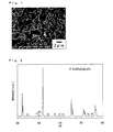
Fig. 1 is a surface observation photograph of 0.97K0.5Na0.5NbO3-0.03K3Nb3O6Si2O7 (Experiment No. 5) taken by a SEM. -
Fig. 2 is a view showing an x-ray diffraction pattern of 0.97K0.5Na0.5NbO3-0.03K3Nb3O6Si2O7 (Experiment No. 6). -
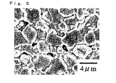
Fig. 3 is a surface observation photograph of 0.97 [K0.5Na0.5]0.96Li0.04Nb0.86Ta0.10Sb0.04O3-0. 03K3Nb3O6Si2O7 (Experiment No. 12). - A piezoelectric ceramic which has an alkali-containing niobic acid-perovskite structure of the present invention includes [K1-xNax]1-yLiy[Nb1-z-wTazSbw]O3 (x, y, z, and w each indicate a molar ratio, and 0≤x<1, 0≤y<1, 0≤z<1, and 0≤w<1 hold) as a primary phase and K3Nb3O6Si2O7 as a subphase.
- Since K3Nb3O6Si2O7 is included as the subphase, an effect in which an internal polycrystalline structure is made fine and homogeneous is obtained. In addition, this effect is obtained regardless of the values of x, y, z, and w.
- In addition, when the piezoelectric ceramic is represented by (1-a) [K1-xNax]1-yLiy[Nb1-z-wTazSbw]O3+aK3Nb3O6Si2O7 (a indicates a molar ratio), it is preferable that 0.003≤a≤0.10 holds, and it is more preferable that 0.006≤a≤0.08 holds.
- The change in significant fine structure can be found out when a≥0.003 holds. However, in the case in which a> 0.10 holds, since K3Nb3O6Si2O7 itself has no piezoelectric effect, when a large amount thereof is precipitated, the piezoelectric properties are degraded as compared to those in the case in which no K3Nb3O6Si2O7 is contained, and although a sintered polycrystalline structure can be made finer, it is difficult to obtain an excellent piezoelectric displacement characteristic.
- The piezoelectric ceramic of the present invention is preferably in a range represented by the formula (1-a)((K1-xNax]1-yLiy) (Nb1-z-wTazSbw)O3+aK3Nb3O6Si2O7 (where x, y, z, and w satisfy 0≤x<1.0, 0≤y≤0.20, 0≤z≤0.40, 0≤w≤0.20, and 0.003≤a≤0.10 hold). When the above ranges are satisfied, a piezoelectric ceramic can be obtained which has an excellent piezoelectric displacement characteristic, a Curie temperature of 150°C or more, and a sufficient resistivity.
- The piezoelectric ceramic of the present invention is more preferably in a range represented by the formula (1-a) ([K1-xNax]1-yLiy) (Nb1-z-wTazSbw)O3+aK3Nb3O6Si2O7 (where x, y, z, and w satisfy 0≤x<1.0, 0≤y≤0.15, 0≤z≤0.20, 0≤w≤0.10, and 0.006≤a≤0.08 hold).
- When the piezoelectric ceramic is in the ranges described above, a high Curie temperature of 200°C or more is obtained; the piezoelectric effect is prevented from being lost at a high temperature; a practical relative dielectric constant (ε), a low dielectric dispersion (tanδ), a high electromechanical coupling coefficient (kr), and a high piezoelectric displacement characteristic (-d31) can be obtained; and its polycrystalline structure is also homogeneous.
- In addition, in the piezoelectric ceramic of the present invention, although it is possible that by addition of a predetermined amount of at least one of Sc, Ti, V, Cr, Mn, Fe, Co, Ni, Cu, and Zn, each of which is a first transition element, the sintering temperature is controlled, the growth of grains is controlled, and the life is increased in a high electric field, these elements may be or may not be used.
- In addition, in the piezoelectric ceramic of the present invention, although it is possible that by addition of a predetermined amount of at least one of Y, Zr, Mo, Ru, Rh, Pd, and Ag, each of which is a second transition element, the sintering temperature is controlled, the growth of grains is controlled, and the life is increased in a high electric field, these elements may be or may not be used.
- In addition, in the piezoelectric ceramic of the present invention, although it is possible that by addition of a predetermined amount of at least one of La, Ce, Pr, Nd, Sm, Eu, Gd, Tb, Dy, Ho, Er, Tm, Yb, Lu, Hf, W, Re, Os, Ir, Pt, and Au, each of which is a third transition element, the sintering temperature is controlled, the growth of grains is controlled, and the life is increased in a high electric field, these elements may be or may not be used.
- Furthermore, although it is possible that by addition of a predetermined amount of at least one of the first, the second, and the third transition elements mentioned above, the sintering temperature is controlled, the growth of grains is controlled, and the life is increased in a high electric field, an effect similar to that described above can be obtained regardless of whether the above elements are used alone or in combination.
- In the present invention, as a method for manufacturing a piezoelectric ceramic, a method may be used which includes a step of obtaining a perovskite composition represented by [K1-xNax]1-yLiy[Nb1-z-wTazSbw]O3 (x, y, z, and w each indicate a molar ratio, and 0≤x<1, 0≤y<1, 0≤z<1, and 0≤w<1 hold); a step of obtaining a composition represented by K3Nb3O6Si2O7; a step of mixing the [K1-xNax]1-yLiy[Nb1-z-wTazSbw]O3 and the K3Nb3O6Si2O7; and a step of molding and firing a mixture therebetween.
- In addition, a method is used which includes a step of obtaining a composition represented by K3Nb3O6Si2O7; a step of blending a material containing potassium, a material containing sodium, a material containing lithium, a material containing niobium, a material containing tantalum, and a material containing antimony to form a perovskite composition represented by [K1-xNax]1-yLiy[Nb1-z-wTazSbw]O3 (x, y, z, and w each indicate a molar ratio, and 0≤x<1, 0≤y<1, 0≤z<1, and 0≤w<1 hold) and mixing this composition with the K3Nb3O6Si2O7; and a step of calcining, molding, and firing a mixture therebetween.
- In this case, as raw materials (materials) realizing the manufacturing method of the present invention, it is preferable that K2CO3 or KHCO3 is used as the material containing potassium, Na2CO3 or NaHCO3 is used as the material containing sodium, Li2CO3 is used as the material containing lithium, Nb2O5 is preferably used as the material containing niobium, Ta2O5 is used as the material containing tantalum, Sb2O3 or Sb2O5 is used as the material containing antimony, and SiO2 is used as a material containing silicon for obtaining K3Nb3O6Si2O7. By using the raw materials described above, the steps of blending, stirring, calcination, and the like can be easily performed, and hence, synthesis can be performed without imposing any loads on the manufacturing.
- In the present invention, calcination is preferably performed at 700°C to 1,000°C, various binders, such as polyvinyl alcohol and polyvinyl butyral, which are generally used may be used as a binder for forming a powder, and firing is preferably performed at 1,040°C to 1,180°C.
- The piezoelectric ceramic of the present invention has a perovskite structure generally represented by AB03. In this structure, the element located at the A-site is at least one of K, Na, an Li, and the element located at the B-site is at least one of Nb, Ta, and Sb. When the stoichiometry is set so that A: B=1: 1 holds, the elements are ideally and completely located at all the site positions, so that a stable structure is obtained. However, as apparent from the constituent elements of the composition, the composition finally changes by approximately several percent, in particular, by 2% or less due to elution of K, Na, and Li by moisture, volatilization of K, Na, and Li in a calcination step, volatilization of K, Na, and Li in a firing step, and the like. The changes of these constituent elements may occur by the changes of the raw materials, synthesis timing, and synthesis process.
- In order to suppress these changes, for example, a technique is used in which the amounts of raw materials used as Na, Li, and Sb sources are intentionally increased in initial blending, and in a final step, that is, in the firing step or a step thereafter, the composition is made close to an ideal state in which A: B=1: 1 holds.
- In order to obtain a ceramic having a high piezoelectric effect, a final ratio of the A-site to the B-site is preferably set so as to satisfy 0.96<A/B<1.002.
- The appropriate adjustment of the amounts of elements intentionally performed in the initial blending as described above is a general technique performed in almost all syntheses of ceramics.
- In the piezoelectric ceramic obtained by the present invention, the relative density of a sintered body is preferably 95% or more.
- Furthermore, in a diffraction pattern which is obtained by x-rays from a powder prepared by pulverizing the sintered body, the ratio of a line intensity of the strongest line of a silicon-containing phase represented by K3Nb3O6Si2O7 to a line intensity of the strongest line of a perovskite compound phase which is a phase exhibiting the piezoelectric effect is preferably 0.3% to 9.0%. Although the composition of the present invention is a piezoelectric ceramic characterized in that K3Nb3O6Si2O7 is precipitated, when the precipitation amount is too small, the polycrystalline structure is not made fine and homogeneous thereby, and when the precipitation amount is large, since the silicon-containing K3Nb3O6Si2O7 phase exhibits no piezoelectric effect, the piezoelectric properties are degraded as described above.
- Hereafter, with reference to examples, the method for manufacturing a piezoelectric ceramic of the present invention and evaluation results will be described.
- In order to evaluate a polycrystalline structure and piezoelectric properties of a piezoelectric ceramic represented by (1-a)K0.5Na0.5NbO3+aK3Nb3O6Si2O7, (where, a=0, 0.003, 0.006, 0.01, 0.03, 0.06, 0.08, 0.1, and 0.12, and corresponding to Experiment Nos. 1 to 9, respectively, in this order), the following experiments were carried out.
- The piezoelectric ceramic of Experiment No. 1 is out of the range of the present invention and is a comparative example. The piezoelectric ceramics of Experiment Nos. 2 to 9 are each within the range of the present invention, and the piezoelectric ceramics of Experiment Nos. 2 to 8 are within the range of a composition formula (1-a) ([K1-xNax]1-yLiy) (Nb1-z-wTazSbw)O3+aK3Nb3O6Si2O7 (where x, y, z, and w satisfy 0≤x<1.0, 0≤y<1, 0≤z<1, 0≤w<1, and 0.003≤a≤0.10 hold).
- As raw materials for the piezoelectric ceramic, K2CO3 (or KHC03), Na2CO3 (or NaHCO3), Nb2O5, Ta2O5, Sb2O3 (or Sb2O5), and K3Nb3O6Si2O7, each having a purity of 99% or more, were prepared and were blended to form a composition which satisfied the chemical stoichiometry shown in Example 1 described above.
- The raw materials thus blended were mixed together in ethanol by a ball mill for 24 hours, and ethanol was then vaporized in a dryer at a temperature of 100°C, thereby obtaining a target raw material mixture. Next, after this raw material mixture was calcined at 950°C for 3 hours, pulverization thereof was performed in ethanol for 24 hours by a ball mill. Subsequently, polyvinyl alcohol was added as a binder, and pelletization was performed.
- After the pelletized powder was pressure molded into a disc having a thickness of 0.6 mm and a diameter of 10 mm, a molded body was fired at 1,080°C to 1,130°C for 2 hours at ordinary pressure in an air atmosphere.
- At this stage, it was confirmed that all the samples of Experiment No. 1 to 9 were sufficiently densified.
- After Ag electrodes were formed by screen-printing on two surfaces of the disc sample thus obtained and were fired at 800°C, an electric field of 3 kV/mm was applied for 15 minutes in an oil bath at 150°C, so that a polarization treatment was performed.
- Subsequently, the disc thus treated was allowed to stand still over one night, the dielectric constant (ε), the dielectric dispersion (tanδ) , the resistivity (p [Ω·cm]), the electromechanical coupling coefficient (kr) in a disc diameter direction, and the piezoelectric displacement characteristic (-d31 [pm/V]) of the disc sample of each of Experiment Nos. 1 to 9 were measured by using a resonance-antiresonance method.
- In addition, in order to observe the polycrystalline structure of the sintered body, a scanning electron microscope (SEM) was used. In order to evaluate the grain diameter, in accordance with a photographic method, an arbitrary number of horizontal lines were drawn on a photograph obtained thereby, and the average length and the maximum length of each of grains intersected by the lines were obtained by an imaging apparatus. Hereinafter, the values thus obtained are regarded as the average grain diameter and the maximum grain diameter. The number of measured grains was set to approximately 400 or more.
- In addition, in order to identify the crystalline phase which precipitated in the obtained polycrystalline, a diffraction pattern by an X-ray diffraction method (hereinafter, abbreviated as XRD) was obtained. The line source used in this case was Cu-Kα rays, 2θ/θ scan was performed using a focused optical system, and a diffraction line pattern in a range of 20°≤2θ≤60° was obtained. In Experiment Nos. 2 to 9, as a fixed phase, a phase having an alkali-containing niobic acid-perovskite structure was confirmed as a primary phase, and precipitation of K3Nb3O6Si2O7 as disclosed in the following Reference Document 1 was confirmed as a subphase (secondary phase).
- In addition, the line strength of the strongest line of the primary phase and the line strength of the strongest line of the secondary phase were evaluated, and the precipitation amount of K3Nb3O6Si2O7 was estimated by the ratio therebetween. That is, the evaluation was performed based on I2/I1=<precipitation amount of K3Nb3O6Si2O7>=<Line intensity of the strongest line of K3Nb3O6Si2O7>/<line intensity of the strongest line of the primary phase>. The individual values thus obtained are collectively shown in Table 1. In addition, the measurement by XRD was performed using RINT-2500/PC manufactured by Rigaku Corp.. Reference Document 1: Powder Diffraction 9(2) 96-97 (1994)
(Table 1) 1
2 3 4 5 6 7 8 9 a 0 0.003 0.006 0.01 0.03 0.06 0.08 0.1 0.12 ε 440 450 460 470 500 580 580 560 480 tan δ 0.074 0.045 0.028 0.024 0.025 0.028 0.036 0.044 0.061 ρ (Ω·cm) 1.40E+10 1.80E+10 9.00E+10 2.70E+11 6.50E+11 5.50E+10 1.60E+10 7.00E+09 3.40E+09 Kr 0.33 0.35 0.38 0.4 0.39 0.36 0.35 0.3 0.24 -d31(pm/V) 38 39 42 46 46 46 44 38 32 AVERAGE GRAIN DIAMETER (µm) 2.8 2.6 1.9 1.5 1.2 0.9 0.9 0.9 0.8 MAXIMUM GRAIN DIAMETER (µm) 12.3 11.2 9.4 5.3 3.7 3.3 3.3 3.1 2.9 I2/I1 (%) 0.0 0.9 1.3 2.0 2.3 4.5 6.5 8.6 11.5 - It was found that since K3Nb3O6Si2O7 was contained in Experiment Nos. 2 to 9, the average grain diameter and the maximum grain diameter were decreased as compared to those of Experiment No. 1 which was a comparative example.
Fig. 1 shows an observation photograph of the surface of the disc sample of Experiment No. 5 taken by a SEM. - In addition, in Experiment Nos. 2 to 7, it was found that compared to Experiment No. 1 which was a comparative example, tanδ was low, ρ was also high, and the electrical properties and the piezoelectric properties, such as kr and -d31, relating to the reliability of a piezoelectric ceramic were improved.
- In Experiment No. 8, since the substitution amount of K3Nb3O6Si2O7 was increased to 0.1 mol, although a decrease in ρ was observed, the average grain diameter was decreased to less than 1 µm, the maximum grain diameter was decreased to 3.1 µm, and hence, the polycrystalline structure was further improved.
- In addition, when the substitution amount of K3Nb3O6Si2O7 was 0.12 mol as in Experiment No. 9, it was found that although the polycrystalline structure was further improved, p, kr, and -d31 became lower than those in Experiment No. 1 which was a comparative example in which a K0.5Na0.5NbO3 simple substance was used. Accordingly, it was found that "a" was preferably in a range of 0.003 to 0.1.
In addition, in Experiment Nos. 2 to 8, I2/I1 was in a range of 0.9% to 8.6%. The diffraction pattern by XRD in Experiment No. 6 is shown inFig. 2 . - Subsequently, the optimal composition ratio of K3Nb3O6Si2O7 was set to 0.03, that is, 0.97 ([K1-xNax]1-yLiy) (Nb1-z-wTazSbw)O3+0.03K3Nb3O6Si2O7 was used, and hereinafter, as Example 2, piezoelectric ceramics having various alkali-containing niobic acid- perovskite structures were evaluated in a manner similar to that described above.
- The compositions of the piezoelectric ceramics used in Example 2 were as follows.
- Experiment No. 10: x=0.50, y=0, z=0.20, and w=0 were satisfied. That is, a piezoelectric ceramic represented by 0.97 [K0.5Na0.5]Nb0.80Ta0.20O3+0.03K3Nb3O6Si2O7 was evaluated.
- Experiment No. 11: x=0.50, y=0.03, z=0.20, and w=0 were satisfied. That is, a piezoelectric ceramic represented by 0.97 [K0.5Na0.5]0.97Li0.03Nb0.80Ta0.20O3+0.03K3Nb3O6Si2O7 was evaluated.
- Experiment No. 12: x=0.50, y=0.04, z=0.10, and w=0.04 were satisfied. That is, a piezoelectric ceramic represented by
0.97 [K0.5Na0.5]0.96Li0.04Nb0.86Ta0.10Sb0.04O3+0.03K3Nb3O6Si2O7 was evaluated. - In addition, Experiment Nos. 13 to 15 were evaluated as comparative examples in a manner similar to that described above, and the case in which K3Nb3O6Si2O7 was not introduced into the piezoelectric ceramic was also evaluated.
- Experiment No. 13 (comparative example): x=0.50, y=0, z=0.20, and w=0 were satisfied. That is, a piezoelectric ceramic represented by [K0.5Na0.5]Nb0.80Ta0.20O3 was evaluated for comparison.
- Experiment No. 14 (comparative example): x=0.50, y=0.03, z=0.20, and w=0 were satisfied. That is, a piezoelectric ceramic represented by [K0.5Na0.5]0.97Li0.03Nb0.80Ta0.20O3 was evaluated for comparison.
- Experiment No. 15 (comparative example): x=0.50, y=0.04, z=0.10, and w=0.04 were satisfied. That is, a piezoelectric ceramic represented by [K0.5Na0.5]0.96Li0.04Nb0.86Ta0.10Sb0.04O3 was evaluated for comparison.
- Also in Example 2, by the same procedure as that in Example 1, after the composition of each of Experiment Nos. 10 to 15 was blended at a stoichiometric ratio, raw materials after blending were mixed together in ethanol for 24 hours by a ball mill, and ethanol was then vaporized in a dryer at 100°C, thereby obtaining respective target raw material mixtures. Next, after these raw material mixtures were each calcined at 950°C for 3 hours, pulverization was performed in ethanol for 24 hours by a ball mill. Subsequently, polyvinyl alcohol was added as a binder, and pelletization was performed.
- After the pelletized powder was pressure molded into a disc having a thickness of 0.6 mm and a diameter of 10 mm, a molded body was fired at 1,080°C to 1,180°C for 2 hours at ordinary pressure in an air atmosphere.
- At this stage, it was confirmed that all the samples of Experiment Nos. 10 to 15 were sufficiently densified.
- Next, as in the case of Example 1, the piezoelectric properties of each sample after the polarization treatment were evaluated, the polycrystalline structure was evaluated, and I2/I1 was evaluated. The results are shown in Table 2.
(Table 2) 10 11 12 131415ε 830 1260 1480 960 1550 1730 tan δ 0.028 0.021 0.025 0.028 0.018 0.02 ρ(Ω·cm) 3.00E+10 9.40E+10 1.20E+11 1.10E+11 9.90E+10 1.40E+11 kr 0.38 0.47 0.47 0.38 0.5 0.47 -d31(pm/V) 61 92 102 63 112 114 AVERAGE GRAIN DIAMETER (µm) 1 0.9 1.7 1.7 1.5 3 MAXIMUM GRAIN DIAMETER (µm) 3.1 2.7 6.5 9 9 27 I2/I1 (%) 2.8 2.7 2.9 0 0 0 - As apparent from Table 2, in all the compositions (comparative example, Experiment Nos. 13 to 15) into which K3Nb3O6Si2O7 was not introduced, although huge grains having a diameter of 9 to 27 µm were dotted in the polycrystalline structure of the ceramic, in all the compositions of Experiment Nos. 10 to 12 each characterized in that K3Nb3O6Si2O7 was contained, all the polycrystalline structures could be homogenized without considerably degrading the piezoelectric displacement characteristic.
- As one observation example, an observation photograph of the surface of the disc sample of Experiment No. 12 taken by a SEM is shown in
Fig. 3 . - By using a ceramic within a range represented by the formula 0.97 ([K1-xNax] 1-yLiy) (Nb1-z-wTazSbw) O3+0. 03K3Nb3O6Si2O7 (where x, y, z, and w satisfy 0≤x<1.0, 0≤y≤0.20, 0≤z≤0.40, and 0≤w<0.20, respectively), which is a piezoelectric ceramic having an alkaline-containing niobic acid perovskite structure in Example 2 and which has a composition range different from that in Example 1, electrical properties and piezoelectric properties, such as ε, tanδ, p, kr, and -d31, evaluation of the average grain diameter and the maximum grain diameter by a SEM, I2/I1 by XRD, and the like were measured as in the measurement performed in Experiment Nos. 1 to 9 and were evaluated, and it was confirmed that as in the case described above, the polycrystalline structure of the above composition could be easily controlled using K3Nb3O6Si2O7.
- As described above, since the internal polycrystalline structure of the piezoelectric ceramic of the present invention is fine and homogeneous, when this piezoelectric ceramic is used for a piezoelectric layer of a piezoelectric device having a conventional laminated structure, that is, is used for a piezoelectric layer of a piezoelectric device in which first electrodes and second electrodes are alternately laminated to each other with piezoelectric ceramic layers interposed therebetween and in which first terminal electrodes electrically connected to the first electrodes and second terminal electrodes electrically connected to the second electrodes are provided, a multilayer formation using many layers can be significantly advantageously performed, the interlayer distance between the layers can be further decreased, and the number of laminations per unit distance can be increased.
Claims (8)
- A piezoelectric ceramic comprising: [K1-xNax]1-yLiy[Nb1-z-wTazSbw]O3 (x, y, z, and w each indicate a molar ratio, and 0≤x<1, 0≤y<1, 0≤z<1, and 0≤w<1 hold) as a primary phase; and K3Nb3O6Si2O7 as a subphase.
- The piezoelectric ceramic according to Claim 1, wherein in the case of (1-a) [K1-xNax]1-yLiy[Nb1-z-wTazSbw]O3+aK3Nb3O6Si2O7 (a indicates a molar ratio), 0.003≤a≤0.10 holds.
- The piezoelectric ceramic according to Claim 1 or 2, wherein when analysis is performed by an X-ray diffraction method, a ratio I2/I1 of a peak intensity I2 of the strongest peak corresponding to a crystalline phase of the K3Nb3O6Si2O7 to a peak intensity I1 of the strongest peak corresponding to a crystalline phase of the [K1-xNax]1-yLiy[Nb1-z-wTazSbw]O3 is 0.8% to 9.0%.
- A piezoelectric device comprising: at least one first electrode and at least one second electrode facing thereto with at least one piezoelectric ceramic layer interposed therebetween, wherein the piezoelectric ceramic layer is formed of the piezoelectric ceramic according to one of Claims 1 and 2.
- The piezoelectric device according to Claim 4, wherein the first electrodes and the second electrodes are alternately laminated to each other with the piezoelectric ceramic layers interposed therebetween, further comprising: first terminal electrodes electrically connected to the first electrodes; and second terminal electrodes electrically connected to the second electrode.
- A method for manufacturing a piezoelectric ceramic comprising: a step of obtaining a perovskite composition represented by [K1-xNax]1-yLiy [Nb1-z-wTazSbw]O3 (x, y, z, and w each indicate a molar ratio, and 0≤x<1, 0≤y<1, 0≤z<1, and 0≤w<1 hold); a step of obtaining a composition represented by K3Nb3O6Si2O7; a step of mixing the [K1-xNax]1-yLiy[Nb1-z-wTazSbw]O3 and the K3Nb3O6Si2O7; and a step of molding and firing a mixture therebetween.
- A method for manufacturing a piezoelectric ceramic comprising: a step of obtaining a composition represented by K3Nb3O6Si2O7; a step of blending a material containing potassium, a material containing sodium, a material containing lithium, a material containing niobium, a material containing tantalum, and a material containing antimony to form a perovskite composition represented by [K1-xNax]1-yLiy[Nb1-z-wTazSbw]O3 (x, y, z, and w each indicate a molar ratio, and 0≤x<1, 0≤y<1, 0≤z<1, and 0≤w<1 hold) and mixing this composition with the K3Nb3O6Si2O7; and a step of calcining, molding, and firing a mixture therebetween.
- The method for manufacturing a piezoelectric ceramic according to Claim 6 or 7, wherein, when the ratio between the [K1-xNax]1-yLiy[Nb1-z-wTazSbw]O3 and the K3Nb3O6Si2O7 is represented by (1-a) [K1-xNax]1-yLiy[Nb1-z-wTazSbw]O3+aK3Nb3O6Si2O7 (a indicates a molar ratio), the mixing is performed so that 0.003 ≤a≤0.10 holds.
Applications Claiming Priority (2)
| Application Number | Priority Date | Filing Date | Title |
|---|---|---|---|
| JP2008221490A JP5214373B2 (en) | 2008-08-29 | 2008-08-29 | Piezoelectric ceramics, manufacturing method thereof, and piezoelectric device |
| PCT/JP2009/064371 WO2010024140A1 (en) | 2008-08-29 | 2009-08-10 | Piezoelectric ceramic, process for producing the piezoelectric ceramic, and piezoelectric device |
Publications (3)
| Publication Number | Publication Date |
|---|---|
| EP2316804A1 true EP2316804A1 (en) | 2011-05-04 |
| EP2316804A4 EP2316804A4 (en) | 2013-09-11 |
| EP2316804B1 EP2316804B1 (en) | 2014-04-23 |
Family
ID=41721309
Family Applications (1)
| Application Number | Title | Priority Date | Filing Date |
|---|---|---|---|
| EP20090809793 Active EP2316804B1 (en) | 2008-08-29 | 2009-08-10 | Piezoelectric ceramic, process for producing the piezoelectric ceramic, and piezoelectric device |
Country Status (6)
| Country | Link |
|---|---|
| US (1) | US8487515B2 (en) |
| EP (1) | EP2316804B1 (en) |
| JP (1) | JP5214373B2 (en) |
| KR (1) | KR101158444B1 (en) |
| CN (1) | CN102131746B (en) |
| WO (1) | WO2010024140A1 (en) |
Families Citing this family (15)
| Publication number | Priority date | Publication date | Assignee | Title |
|---|---|---|---|---|
| JP2010053021A (en) * | 2008-07-28 | 2010-03-11 | Ngk Insulators Ltd | Piezoelectric/electrostrictive ceramic sintered body and method of calculating diffuse scattering intensity ratio |
| EP2431343B1 (en) * | 2009-05-08 | 2016-09-14 | Taiyo Yuden Co., Ltd. | Piezoelectric ceramic, method for producing same, and piezoelectric device |
| CN102010195B (en) * | 2010-09-03 | 2013-04-03 | 中国地质大学(北京) | Zirconium and molybdenum-doped bismuth layer-shaped leadless piezoelectric ceramic material and preparation method thereof |
| JP5711990B2 (en) * | 2011-02-03 | 2015-05-07 | Fdk株式会社 | Piezoelectric equipment |
| JP5662888B2 (en) | 2011-07-04 | 2015-02-04 | 太陽誘電株式会社 | Multi-layer piezoelectric ceramic parts |
| JP5476344B2 (en) * | 2011-07-28 | 2014-04-23 | 日本特殊陶業株式会社 | Dielectric porcelain composition, capacitor, and method for producing dielectric porcelain composition |
| WO2013094368A1 (en) * | 2011-12-20 | 2013-06-27 | 太陽誘電株式会社 | Piezoelectric device and piezoelectric ceramic composition |
| JP5929640B2 (en) * | 2011-12-26 | 2016-06-08 | Tdk株式会社 | Piezoelectric ceramic and piezoelectric element |
| JP5543537B2 (en) | 2012-07-24 | 2014-07-09 | 太陽誘電株式会社 | Piezoelectric element |
| JP5704725B2 (en) | 2012-08-24 | 2015-04-22 | 太陽誘電株式会社 | Piezoelectric ceramics and piezoelectric element |
| JP6327914B2 (en) | 2014-04-11 | 2018-05-23 | 日本特殊陶業株式会社 | Lead-free piezoelectric ceramic composition, piezoelectric element using the same, and lead-free piezoelectric ceramic composition manufacturing method |
| US11631801B2 (en) * | 2019-03-29 | 2023-04-18 | Taiyo Yuden Co., Ltd. | Multilayer piezoelectric ceramic and method for manufacturing same, multilayer piezoelectric element, as well as piezoelectric vibration device |
| CN115490514B (en) * | 2021-06-18 | 2023-07-11 | 阜新德尔汽车部件股份有限公司 | Piezoelectric ceramic and preparation method and application thereof |
| CN113429205B (en) * | 2021-07-16 | 2022-04-01 | 桂林电子科技大学 | A kind of transparent down-conversion photoluminescence ceramic material and its preparation method and application |
| CN116354719B (en) * | 2023-03-28 | 2024-05-28 | 南充三环电子有限公司 | A potassium sodium niobate-based ceramic and its preparation method and application |
Family Cites Families (22)
| Publication number | Priority date | Publication date | Assignee | Title |
|---|---|---|---|---|
| DE3246592C1 (en) | 1982-12-16 | 1983-10-27 | Eppendorf Gerätebau Netheler + Hinz GmbH, 2000 Hamburg | Envelope for mixing and for optical examinations |
| IT1161138B (en) | 1983-04-13 | 1987-03-11 | Instrumentation Lab Spa | CENTRIFUGAL ANALYTICAL PHOTOMETER, SUITABLE FOR THE PRACTICALLY SIMULTANEOUS DETERMINATION OF THE PRESENCE OF DIFFERENT SUBSTANCES IN A CERTAIN NUMBER OF DISCRETE SAMPLES |
| JP4569491B2 (en) | 1998-09-28 | 2010-10-27 | 日産自動車株式会社 | Piezoelectric actuator |
| JP3613140B2 (en) | 1999-08-26 | 2005-01-26 | 株式会社村田製作所 | Piezoelectric ceramic composition and piezoelectric ceramic element using the same |
| JP2002241175A (en) | 2001-02-13 | 2002-08-28 | Kazuo Shoji | Piezoelectric material provided with high mechanical quality factor |
| JP2003201172A (en) | 2001-10-24 | 2003-07-15 | National Institute Of Advanced Industrial & Technology | Lead-free piezoelectric ceramic composition and method for producing the same |
| US7101491B2 (en) * | 2002-07-16 | 2006-09-05 | Denso Corporation | Piezoelectric ceramic composition and method of production of same, piezoelectric element, and dielectric element |
| JP2004075448A (en) | 2002-08-15 | 2004-03-11 | Taiyo Yuden Co Ltd | Piezoelectric ceramic composition, method of manufacturing piezoelectric ceramic composition and piezoelectric ceramic part |
| JP4177615B2 (en) | 2002-08-15 | 2008-11-05 | 太陽誘電株式会社 | Piezoelectric ceramic composition, piezoelectric ceramic composition manufacturing method, and piezoelectric ceramic component |
| JP2004161532A (en) | 2002-11-13 | 2004-06-10 | National Institute Of Advanced Industrial & Technology | Polycrystalline piezoelectric material and method of manufacturing the same |
| JP4510140B2 (en) | 2003-01-23 | 2010-07-21 | 株式会社デンソー | Piezoelectric ceramic composition, piezoelectric element and dielectric element |
| JP4449331B2 (en) * | 2003-04-28 | 2010-04-14 | 株式会社村田製作所 | Piezoelectric ceramic and piezoelectric ceramic element using the same |
| JP2004359539A (en) | 2003-05-09 | 2004-12-24 | Nagoya Industrial Science Research Inst | Method of manufacturing potassium niobate sintered compact |
| JP2006062955A (en) | 2004-07-30 | 2006-03-09 | Toko Inc | Piezoelectric ceramic |
| EP1642875A3 (en) * | 2004-09-29 | 2009-01-28 | Ngk Insulators, Ltd. | Piezoelectric/electrostrictive porcelain composition, piezoelectric/electrostrictive article, and piezoelectric/electrostrictive film type element |
| JP4044943B2 (en) | 2005-04-28 | 2008-02-06 | 本多電子株式会社 | Piezoelectric ceramic material |
| JP4044944B2 (en) | 2005-05-26 | 2008-02-06 | 本多電子株式会社 | Piezoelectric ceramic materials |
| JP4281726B2 (en) | 2005-10-11 | 2009-06-17 | 株式会社村田製作所 | Piezoelectric ceramic composition, piezoelectric ceramic and piezoelectric ceramic element |
| JP2007204336A (en) | 2006-02-03 | 2007-08-16 | Denso Corp | Lead-free piezoelectric ceramics |
| JP4595889B2 (en) * | 2006-06-05 | 2010-12-08 | 日立電線株式会社 | Method for manufacturing piezoelectric thin film element |
| JP2008050206A (en) * | 2006-08-24 | 2008-03-06 | Seiko Epson Corp | Piezoelectric material, manufacturing method thereof, and piezoelectric element |
| EP2431343B1 (en) | 2009-05-08 | 2016-09-14 | Taiyo Yuden Co., Ltd. | Piezoelectric ceramic, method for producing same, and piezoelectric device |
-
2008
- 2008-08-29 JP JP2008221490A patent/JP5214373B2/en active Active
-
2009
- 2009-08-10 EP EP20090809793 patent/EP2316804B1/en active Active
- 2009-08-10 US US13/060,253 patent/US8487515B2/en active Active
- 2009-08-10 WO PCT/JP2009/064371 patent/WO2010024140A1/en not_active Ceased
- 2009-08-10 CN CN2009801334168A patent/CN102131746B/en active Active
- 2009-08-10 KR KR1020107029234A patent/KR101158444B1/en not_active Expired - Fee Related
Also Published As
| Publication number | Publication date |
|---|---|
| CN102131746A (en) | 2011-07-20 |
| WO2010024140A1 (en) | 2010-03-04 |
| KR20110014225A (en) | 2011-02-10 |
| US8487515B2 (en) | 2013-07-16 |
| JP2010052999A (en) | 2010-03-11 |
| JP5214373B2 (en) | 2013-06-19 |
| EP2316804A4 (en) | 2013-09-11 |
| US20110156540A1 (en) | 2011-06-30 |
| EP2316804B1 (en) | 2014-04-23 |
| CN102131746B (en) | 2013-07-10 |
| KR101158444B1 (en) | 2012-06-22 |
Similar Documents
| Publication | Publication Date | Title |
|---|---|---|
| EP2316804B1 (en) | Piezoelectric ceramic, process for producing the piezoelectric ceramic, and piezoelectric device | |
| JP5576365B2 (en) | Piezoelectric ceramics, manufacturing method thereof, and piezoelectric device | |
| Herabut et al. | Processing and electromechanical properties of (Bi0. 5Na0. 5)(1− 1.5 x) LaxTiO3 ceramics | |
| EP1876155B1 (en) | Piezoelectric porcelain composition and piezoelectric ceramic electronic component | |
| US8518290B2 (en) | Piezoelectric material | |
| JP5782457B2 (en) | Piezoelectric ceramics, piezoelectric ceramic component, and piezoelectric device using the piezoelectric ceramic component | |
| EP2610233B1 (en) | Piezoelectric ceramic and piezoelectric device | |
| JPWO2013175740A1 (en) | Piezoelectric composition and manufacturing method thereof, piezoelectric element / lead-free piezoelectric element and manufacturing method thereof, ultrasonic probe, and diagnostic imaging apparatus | |
| JP2009114037A (en) | Method for producing crystal-oriented ceramics | |
| Mao et al. | Low-Temperature Sintering Properties of Bi2O3 Doped PZT-5H Piezoelectric Ceramics: W. Mao et al. | |
| US20080067897A1 (en) | Production Method of Piezoelectric Ceramic, Production Method of Piezoelectric Element, and Piezoelectric Element | |
| JP2010222185A (en) | Method for producing anisotropically shaped powder and crystallographically oriented ceramics | |
| JP2002284574A (en) | Manufacturing method of piezoelectric ceramic | |
| Kim et al. | Effects of Zn/Ni ratio and doping material on piezoelectric characteristics of Pb ((Zn, Ni) 1/3Nb2/3) O3–Pb (Zr, Ti) O3 ceramics | |
| KR102828325B1 (en) | Lead-free piezoelectric ceramics with high energy conversion efficiency and precision control valves using the same | |
| CN120864877A (en) | Barium titanate-based lead-free piezoelectric ceramic with high piezoelectric coefficient and preparation method and application thereof | |
| JP2009114038A (en) | Method for producing crystal-oriented ceramics | |
| JP2014209642A (en) | Lamination type electronic part, and manufacturing method thereof | |
| JP2007302494A (en) | Crystalline oriented ceramics and method for producing |
Legal Events
| Date | Code | Title | Description |
|---|---|---|---|
| PUAI | Public reference made under article 153(3) epc to a published international application that has entered the european phase |
Free format text: ORIGINAL CODE: 0009012 |
|
| 17P | Request for examination filed |
Effective date: 20101223 |
|
| AK | Designated contracting states |
Kind code of ref document: A1 Designated state(s): AT BE BG CH CY CZ DE DK EE ES FI FR GB GR HR HU IE IS IT LI LT LU LV MC MK MT NL NO PL PT RO SE SI SK SM TR |
|
| AX | Request for extension of the european patent |
Extension state: AL BA RS |
|
| DAX | Request for extension of the european patent (deleted) | ||
| A4 | Supplementary search report drawn up and despatched |
Effective date: 20130813 |
|
| RIC1 | Information provided on ipc code assigned before grant |
Ipc: H01L 41/187 20060101ALI20130805BHEP Ipc: H01L 41/43 20130101ALI20130805BHEP Ipc: C04B 35/63 20060101ALI20130805BHEP Ipc: C04B 35/495 20060101AFI20130805BHEP Ipc: H01L 41/083 20060101ALI20130805BHEP Ipc: H03H 9/17 20060101ALI20130805BHEP |
|
| REG | Reference to a national code |
Ref country code: DE Ref legal event code: R079 Ref document number: 602009023555 Country of ref document: DE Free format text: PREVIOUS MAIN CLASS: C04B0035000000 Ipc: C04B0035495000 |
|
| RIC1 | Information provided on ipc code assigned before grant |
Ipc: H01L 41/083 20060101ALI20131009BHEP Ipc: H01L 41/43 20130101ALI20131009BHEP Ipc: C04B 35/626 20060101ALI20131009BHEP Ipc: H01L 41/187 20060101ALI20131009BHEP Ipc: C04B 35/495 20060101AFI20131009BHEP |
|
| GRAP | Despatch of communication of intention to grant a patent |
Free format text: ORIGINAL CODE: EPIDOSNIGR1 |
|
| INTG | Intention to grant announced |
Effective date: 20131127 |
|
| GRAS | Grant fee paid |
Free format text: ORIGINAL CODE: EPIDOSNIGR3 |
|
| GRAA | (expected) grant |
Free format text: ORIGINAL CODE: 0009210 |
|
| AK | Designated contracting states |
Kind code of ref document: B1 Designated state(s): AT BE BG CH CY CZ DE DK EE ES FI FR GB GR HR HU IE IS IT LI LT LU LV MC MK MT NL NO PL PT RO SE SI SK SM TR |
|
| REG | Reference to a national code |
Ref country code: GB Ref legal event code: FG4D |
|
| REG | Reference to a national code |
Ref country code: CH Ref legal event code: EP |
|
| REG | Reference to a national code |
Ref country code: AT Ref legal event code: REF Ref document number: 663732 Country of ref document: AT Kind code of ref document: T Effective date: 20140515 |
|
| REG | Reference to a national code |
Ref country code: IE Ref legal event code: FG4D |
|
| REG | Reference to a national code |
Ref country code: DE Ref legal event code: R096 Ref document number: 602009023555 Country of ref document: DE Effective date: 20140605 |
|
| REG | Reference to a national code |
Ref country code: AT Ref legal event code: MK05 Ref document number: 663732 Country of ref document: AT Kind code of ref document: T Effective date: 20140423 |
|
| REG | Reference to a national code |
Ref country code: NL Ref legal event code: VDEP Effective date: 20140423 |
|
| REG | Reference to a national code |
Ref country code: LT Ref legal event code: MG4D |
|
| PG25 | Lapsed in a contracting state [announced via postgrant information from national office to epo] |
Ref country code: LT Free format text: LAPSE BECAUSE OF FAILURE TO SUBMIT A TRANSLATION OF THE DESCRIPTION OR TO PAY THE FEE WITHIN THE PRESCRIBED TIME-LIMIT Effective date: 20140423 Ref country code: BG Free format text: LAPSE BECAUSE OF FAILURE TO SUBMIT A TRANSLATION OF THE DESCRIPTION OR TO PAY THE FEE WITHIN THE PRESCRIBED TIME-LIMIT Effective date: 20140723 Ref country code: FI Free format text: LAPSE BECAUSE OF FAILURE TO SUBMIT A TRANSLATION OF THE DESCRIPTION OR TO PAY THE FEE WITHIN THE PRESCRIBED TIME-LIMIT Effective date: 20140423 Ref country code: GR Free format text: LAPSE BECAUSE OF FAILURE TO SUBMIT A TRANSLATION OF THE DESCRIPTION OR TO PAY THE FEE WITHIN THE PRESCRIBED TIME-LIMIT Effective date: 20140724 Ref country code: CY Free format text: LAPSE BECAUSE OF FAILURE TO SUBMIT A TRANSLATION OF THE DESCRIPTION OR TO PAY THE FEE WITHIN THE PRESCRIBED TIME-LIMIT Effective date: 20140423 Ref country code: IS Free format text: LAPSE BECAUSE OF FAILURE TO SUBMIT A TRANSLATION OF THE DESCRIPTION OR TO PAY THE FEE WITHIN THE PRESCRIBED TIME-LIMIT Effective date: 20140823 Ref country code: NO Free format text: LAPSE BECAUSE OF FAILURE TO SUBMIT A TRANSLATION OF THE DESCRIPTION OR TO PAY THE FEE WITHIN THE PRESCRIBED TIME-LIMIT Effective date: 20140723 Ref country code: NL Free format text: LAPSE BECAUSE OF FAILURE TO SUBMIT A TRANSLATION OF THE DESCRIPTION OR TO PAY THE FEE WITHIN THE PRESCRIBED TIME-LIMIT Effective date: 20140423 |
|
| PG25 | Lapsed in a contracting state [announced via postgrant information from national office to epo] |
Ref country code: LV Free format text: LAPSE BECAUSE OF FAILURE TO SUBMIT A TRANSLATION OF THE DESCRIPTION OR TO PAY THE FEE WITHIN THE PRESCRIBED TIME-LIMIT Effective date: 20140423 Ref country code: PL Free format text: LAPSE BECAUSE OF FAILURE TO SUBMIT A TRANSLATION OF THE DESCRIPTION OR TO PAY THE FEE WITHIN THE PRESCRIBED TIME-LIMIT Effective date: 20140423 Ref country code: SE Free format text: LAPSE BECAUSE OF FAILURE TO SUBMIT A TRANSLATION OF THE DESCRIPTION OR TO PAY THE FEE WITHIN THE PRESCRIBED TIME-LIMIT Effective date: 20140423 Ref country code: AT Free format text: LAPSE BECAUSE OF FAILURE TO SUBMIT A TRANSLATION OF THE DESCRIPTION OR TO PAY THE FEE WITHIN THE PRESCRIBED TIME-LIMIT Effective date: 20140423 Ref country code: ES Free format text: LAPSE BECAUSE OF FAILURE TO SUBMIT A TRANSLATION OF THE DESCRIPTION OR TO PAY THE FEE WITHIN THE PRESCRIBED TIME-LIMIT Effective date: 20140423 Ref country code: HR Free format text: LAPSE BECAUSE OF FAILURE TO SUBMIT A TRANSLATION OF THE DESCRIPTION OR TO PAY THE FEE WITHIN THE PRESCRIBED TIME-LIMIT Effective date: 20140423 |
|
| PG25 | Lapsed in a contracting state [announced via postgrant information from national office to epo] |
Ref country code: PT Free format text: LAPSE BECAUSE OF FAILURE TO SUBMIT A TRANSLATION OF THE DESCRIPTION OR TO PAY THE FEE WITHIN THE PRESCRIBED TIME-LIMIT Effective date: 20140825 |
|
| REG | Reference to a national code |
Ref country code: DE Ref legal event code: R097 Ref document number: 602009023555 Country of ref document: DE |
|
| PG25 | Lapsed in a contracting state [announced via postgrant information from national office to epo] |
Ref country code: EE Free format text: LAPSE BECAUSE OF FAILURE TO SUBMIT A TRANSLATION OF THE DESCRIPTION OR TO PAY THE FEE WITHIN THE PRESCRIBED TIME-LIMIT Effective date: 20140423 Ref country code: DK Free format text: LAPSE BECAUSE OF FAILURE TO SUBMIT A TRANSLATION OF THE DESCRIPTION OR TO PAY THE FEE WITHIN THE PRESCRIBED TIME-LIMIT Effective date: 20140423 Ref country code: SK Free format text: LAPSE BECAUSE OF FAILURE TO SUBMIT A TRANSLATION OF THE DESCRIPTION OR TO PAY THE FEE WITHIN THE PRESCRIBED TIME-LIMIT Effective date: 20140423 Ref country code: CZ Free format text: LAPSE BECAUSE OF FAILURE TO SUBMIT A TRANSLATION OF THE DESCRIPTION OR TO PAY THE FEE WITHIN THE PRESCRIBED TIME-LIMIT Effective date: 20140423 Ref country code: RO Free format text: LAPSE BECAUSE OF FAILURE TO SUBMIT A TRANSLATION OF THE DESCRIPTION OR TO PAY THE FEE WITHIN THE PRESCRIBED TIME-LIMIT Effective date: 20140423 Ref country code: BE Free format text: LAPSE BECAUSE OF FAILURE TO SUBMIT A TRANSLATION OF THE DESCRIPTION OR TO PAY THE FEE WITHIN THE PRESCRIBED TIME-LIMIT Effective date: 20140423 |
|
| PLBE | No opposition filed within time limit |
Free format text: ORIGINAL CODE: 0009261 |
|
| STAA | Information on the status of an ep patent application or granted ep patent |
Free format text: STATUS: NO OPPOSITION FILED WITHIN TIME LIMIT |
|
| PG25 | Lapsed in a contracting state [announced via postgrant information from national office to epo] |
Ref country code: IT Free format text: LAPSE BECAUSE OF FAILURE TO SUBMIT A TRANSLATION OF THE DESCRIPTION OR TO PAY THE FEE WITHIN THE PRESCRIBED TIME-LIMIT Effective date: 20140423 Ref country code: MC Free format text: LAPSE BECAUSE OF FAILURE TO SUBMIT A TRANSLATION OF THE DESCRIPTION OR TO PAY THE FEE WITHIN THE PRESCRIBED TIME-LIMIT Effective date: 20140423 Ref country code: LU Free format text: LAPSE BECAUSE OF FAILURE TO SUBMIT A TRANSLATION OF THE DESCRIPTION OR TO PAY THE FEE WITHIN THE PRESCRIBED TIME-LIMIT Effective date: 20140810 |
|
| REG | Reference to a national code |
Ref country code: CH Ref legal event code: PL |
|
| 26N | No opposition filed |
Effective date: 20150126 |
|
| GBPC | Gb: european patent ceased through non-payment of renewal fee |
Effective date: 20140810 |
|
| PG25 | Lapsed in a contracting state [announced via postgrant information from national office to epo] |
Ref country code: CH Free format text: LAPSE BECAUSE OF NON-PAYMENT OF DUE FEES Effective date: 20140831 Ref country code: LI Free format text: LAPSE BECAUSE OF NON-PAYMENT OF DUE FEES Effective date: 20140831 |
|
| REG | Reference to a national code |
Ref country code: DE Ref legal event code: R097 Ref document number: 602009023555 Country of ref document: DE Effective date: 20150126 |
|
| REG | Reference to a national code |
Ref country code: IE Ref legal event code: MM4A |
|
| REG | Reference to a national code |
Ref country code: FR Ref legal event code: ST Effective date: 20150430 |
|
| PG25 | Lapsed in a contracting state [announced via postgrant information from national office to epo] |
Ref country code: GB Free format text: LAPSE BECAUSE OF NON-PAYMENT OF DUE FEES Effective date: 20140810 Ref country code: SI Free format text: LAPSE BECAUSE OF FAILURE TO SUBMIT A TRANSLATION OF THE DESCRIPTION OR TO PAY THE FEE WITHIN THE PRESCRIBED TIME-LIMIT Effective date: 20140423 |
|
| PG25 | Lapsed in a contracting state [announced via postgrant information from national office to epo] |
Ref country code: IE Free format text: LAPSE BECAUSE OF NON-PAYMENT OF DUE FEES Effective date: 20140810 Ref country code: FR Free format text: LAPSE BECAUSE OF NON-PAYMENT OF DUE FEES Effective date: 20140901 |
|
| PG25 | Lapsed in a contracting state [announced via postgrant information from national office to epo] |
Ref country code: SM Free format text: LAPSE BECAUSE OF FAILURE TO SUBMIT A TRANSLATION OF THE DESCRIPTION OR TO PAY THE FEE WITHIN THE PRESCRIBED TIME-LIMIT Effective date: 20140423 |
|
| PG25 | Lapsed in a contracting state [announced via postgrant information from national office to epo] |
Ref country code: MT Free format text: LAPSE BECAUSE OF FAILURE TO SUBMIT A TRANSLATION OF THE DESCRIPTION OR TO PAY THE FEE WITHIN THE PRESCRIBED TIME-LIMIT Effective date: 20140423 |
|
| PG25 | Lapsed in a contracting state [announced via postgrant information from national office to epo] |
Ref country code: HU Free format text: LAPSE BECAUSE OF FAILURE TO SUBMIT A TRANSLATION OF THE DESCRIPTION OR TO PAY THE FEE WITHIN THE PRESCRIBED TIME-LIMIT; INVALID AB INITIO Effective date: 20090810 Ref country code: TR Free format text: LAPSE BECAUSE OF FAILURE TO SUBMIT A TRANSLATION OF THE DESCRIPTION OR TO PAY THE FEE WITHIN THE PRESCRIBED TIME-LIMIT Effective date: 20140423 |
|
| PG25 | Lapsed in a contracting state [announced via postgrant information from national office to epo] |
Ref country code: MK Free format text: LAPSE BECAUSE OF FAILURE TO SUBMIT A TRANSLATION OF THE DESCRIPTION OR TO PAY THE FEE WITHIN THE PRESCRIBED TIME-LIMIT Effective date: 20140423 |
|
| P01 | Opt-out of the competence of the unified patent court (upc) registered |
Effective date: 20230509 |
|
| PGFP | Annual fee paid to national office [announced via postgrant information from national office to epo] |
Ref country code: DE Payment date: 20250702 Year of fee payment: 17 |