EP2315246A1 - Integrated circuit - Google Patents
Integrated circuit Download PDFInfo
- Publication number
- EP2315246A1 EP2315246A1 EP09173771A EP09173771A EP2315246A1 EP 2315246 A1 EP2315246 A1 EP 2315246A1 EP 09173771 A EP09173771 A EP 09173771A EP 09173771 A EP09173771 A EP 09173771A EP 2315246 A1 EP2315246 A1 EP 2315246A1
- Authority
- EP
- European Patent Office
- Prior art keywords
- active region
- integrated circuit
- electrode
- metal contact
- interconnect level
- Prior art date
- Legal status (The legal status is an assumption and is not a legal conclusion. Google has not performed a legal analysis and makes no representation as to the accuracy of the status listed.)
- Granted
Links
Images



Classifications
-
- H—ELECTRICITY
- H10—SEMICONDUCTOR DEVICES; ELECTRIC SOLID-STATE DEVICES NOT OTHERWISE PROVIDED FOR
- H10D—INORGANIC ELECTRIC SEMICONDUCTOR DEVICES
- H10D8/00—Diodes
- H10D8/60—Schottky-barrier diodes
-
- H—ELECTRICITY
- H10—SEMICONDUCTOR DEVICES; ELECTRIC SOLID-STATE DEVICES NOT OTHERWISE PROVIDED FOR
- H10D—INORGANIC ELECTRIC SEMICONDUCTOR DEVICES
- H10D8/00—Diodes
- H10D8/01—Manufacture or treatment
- H10D8/051—Manufacture or treatment of Schottky diodes
-
- H—ELECTRICITY
- H10—SEMICONDUCTOR DEVICES; ELECTRIC SOLID-STATE DEVICES NOT OTHERWISE PROVIDED FOR
- H10D—INORGANIC ELECTRIC SEMICONDUCTOR DEVICES
- H10D62/00—Semiconductor bodies, or regions thereof, of devices having potential barriers
- H10D62/10—Shapes, relative sizes or dispositions of the regions of the semiconductor bodies; Shapes of the semiconductor bodies
- H10D62/13—Semiconductor regions connected to electrodes carrying current to be rectified, amplified or switched, e.g. source or drain regions
- H10D62/141—Anode or cathode regions of thyristors; Collector or emitter regions of gated bipolar-mode devices, e.g. of IGBTs
-
- H—ELECTRICITY
- H10—SEMICONDUCTOR DEVICES; ELECTRIC SOLID-STATE DEVICES NOT OTHERWISE PROVIDED FOR
- H10D—INORGANIC ELECTRIC SEMICONDUCTOR DEVICES
- H10D84/00—Integrated devices formed in or on semiconductor substrates that comprise only semiconducting layers, e.g. on Si wafers or on GaAs-on-Si wafers
- H10D84/80—Integrated devices formed in or on semiconductor substrates that comprise only semiconducting layers, e.g. on Si wafers or on GaAs-on-Si wafers characterised by the integration of at least one component covered by groups H10D12/00 or H10D30/00, e.g. integration of IGFETs
- H10D84/811—Combinations of field-effect devices and one or more diodes, capacitors or resistors
Definitions
- This invention relates to an integrated circuit and to a method of making an integrated circuit.
- Diodes are well known the art for their rectifying properties, whereby current is allowed to pass only in a single direction through the device. With reference to Figures 1A and 1B , the properties of the ideal diode and a typical real-world diode are briefly compared.
- Figure 1B shows that below a characteristic forward bias switch- on voltage V f , the current flowing through the diode for V > 0 remains substantially at zero. The current in the device rises exponentially above V f .
- An alternative way of viewing the behaviour of the ideal diode shown in Figure 1A is to treat V f as essentially equal to zero.
- a small reverse current flows through the diode, such that the diode does not act as a perfect rectifier (current may pass through the diode in either direction, but is limited to I RB in the reverse direction).
- V f , I RB , and V BR depend on the design of the diode, and can be tailored according to design requirements by altering parameters such as the doping levels and work functions of the materials used within the device.
- diodes that have a low value of V f .
- V f For example, to rectify an AC signal with a small amplitude, a small V f is necessary in order to have any output signal (V f should be smaller than the AC signal amplitude).
- a more specific example is the charge pump circuit, which can be used for rectification and amplification purposes in an RFID tag (an example of this can be found at www.eecg.utoronto.ca/ ⁇ kphang/ece1371/chargepumps.pdf).
- V f in order to have an output voltage, V f should be lower than V in .
- V in depends on the distance between RF signal emitter and receiver (the longer the distance between them, the smaller the V in )
- having a low V f implies that the RFID can operate at even greater distances.
- a low V f implies higher power efficiency (how much of the input signal will pass through the diode).
- Schottky diodes which typically do have low values of V f , are therefore particularly suitable.
- Schottky diodes typically include a metal-semiconductor junction, which forms the basis for the rectifying action of the diode.
- CMOS processing e.g. for incorporation into the die of an RFID tag
- an integrated circuit including a Schottky diode.
- the diode comprises an active region bordered by an isolation region in a semiconductor substrate of the integrated circuit.
- the diode also comprises a first electrode comprising a metal contact provided on a surface of the active region.
- the diode further comprises a second electrode comprising a silicide contact also provided on said surface of said active region.
- a method of making an integrated circuit including a Schottky diode comprises providing a semiconductor substrate.
- the method also comprises providing an isolation region in the substrate, wherein the isolation borders an active region of the substrate.
- the method further comprises forming a metal contact on a surface of the active region to provide a first electrode of the diode.
- the method also comprises forming a silicide contact on said surface of said active region to provide a second electrode of the diode.
- the invention allows the provision of a Schottky diode in an integrated circuit, using a novel combination of standard CMOS processing techniques. Accordingly, manufacture of the diode can be integrated into middle or back end of line process flows.
- the isolation region comprises shallow trench isolation.
- the active region can include a doped well.
- the first and second electrodes in this example can be provided on the surface of the active region above the doped well.
- the doped well can be formed by ion implantation.
- a portion of the surface of the active region is covered by a protection layer comprising, for example, a nitride layer.
- the metal contact can extend through an opening (formed by, for example, an etching process) in the protection layer, to meet the surface of the active region.
- the silicide contact can be provided on an exposed portion of the surface of the active region that is not covered by the protection layer.
- the protection layer serves to protect the non-exposed portions of the surface from the silicidation process.
- the diode can include a portion of semiconductor material located in the active region, adjacent the edges of the metal contact of the first electrode. This can reduce leakage current at the edges of the metal contact.
- the portion of semiconductor material can be more highly doped than the remainder of the active region.
- the portion of semiconductor material can also have a conductivity type opposite to that of the remainder of the active region. The portion of semiconductor material adjacent can form a closed ring around the metal contact, again minimising leakage currents.
- the metal contact of the first electrode can comprise a portion of an interconnect level of the substrate.
- the metal composition of the interconnect determines the work function of the first electrode, thus influencing factors such as the switch on voltage V f of the diode.
- the interconnect level can be a local interconnect level of the substrate, or a lowest metal interconnect level (M1) of the substrate. This conveniently allows the manufacture of the diode to be integrated in middle end or back end of line process flows.
- an RFID tag including an integrated circuit of the kind described above.
- a method of making an RFID tag includes the method described above for making an integrated circuit of the RFID tag.
- This invention can provide an integrated circuit comprising a diode, such as a Schottky diode, which can be manufactured using standard CMOS processing techniques.
- a diode in accordance with this invention can be manufactured as part of a middle or back end of line process flow.
- a first embodiment of a method for making an integrated circuit comprising a Schottky diode is described below in relation to Figure 2 .
- a semiconductor substrate 2 In a first stage of the method, there is provided a semiconductor substrate 2.
- the substrate 2 may comprise any suitable material, for example silicon.
- Trenches 4 are formed in a major surface of the substrate 2 using, for example, one or more conventional masking and etching steps.
- the trenches 4 may be filled with an insulating material.
- the trenches 4 may, for example, be shallow trench isolation (STI) trenches.
- STI shallow trench isolation
- the trenches 4 define an active region 6 of the substrate 2.
- the active region 6 is bordered by the trenches 4, which can constitute an isolation region in the substrate 2, isolating the active region 6 from other parts of the substrate 2.
- the active region 6 bordered by the trenches 4 may have a substantially oblong shape, although other shapes may also be used (for example, hexagonal, square, circle etc.).
- a well implantation step I 1 is performed, to dope the active region 6.
- Either n-type or p-type doping may be used, according to design requirements for the diode.
- a further implantation step I 2 is then performed, to form doped contact implants 8.
- the contact implants 8 will have a conductivity type that is the same as that of the doped active region 6.
- the contact implant 8 can be doped to a higher level than the remainder of the active region 6, thereby to enable silicidation to ensure the provision of ohmic contacts.
- a protection layer 14 is then formed on the surface of the active region 6. This layer 14 protects the surface of the active region 6 during the subsequent silicidation step.
- the protection layer 14 is formed in a gap in between the contact implants 8.
- the protection layer 14 may, for example, comprise a nitride layer. Thereafter, the contact implants 8 are silicidated to form the silicide contacts 12.
- metal contacts 16 and 18 are formed.
- the contacts 18 connect to the silicide contacts 12, while the contact 16 makes direct contact with the surface of the doped active region 6.
- the contact 16 passes through an opening provided in the protection layer 14.
- the opening can be formed using, for example, an etching step.
- a diode can comprise a semiconductor substrate 2 having an active region 6 that is bordered by an isolation region (such as the trenches 4).
- a first electrode 16 of the diode comprises a metal contact that is provided on a surface of the active region 6.
- a second electrode of the diode comprises a silicide contact 12 that is also provided on the surface of the active region 6.
- a third implantation step I 3 is performed to form a semiconductor portion 20, which has a conductivity type which is opposite to the conductivity type of the doped active portion 6.
- the semiconductor portion 20 in this example is located in between the contact implants 8.
- the semiconductor portion 20 may also have a higher doping level than the remainder of the active region 6.
- the portion of semiconductor material 20 is provided adjacent the edges of the metal contact 16.
- the provision of the portion of semiconductor material 20 having a conductivity type opposite to that of the remainder of the active region 6 aids in reducing leakage currents.
- the junction between the active region 6 (which has a first conductivity type) and the portion 20 (which has a conductivity type opposite to the first conductivity type) blocks such leakage currents.
- the portion of semiconductor material 20 can substantially surround the metal contact 16 in the region at which the metal contact 16 meets the surface of the active region 6, forming a closed ring.
- the portion of semiconductor material 20 can overlap the edges of the metal contact 16. This enhances the ability of the portion of semiconductor material 20 to inhibit leakage currents, since extra leakage currents normally arise from the Schottky contact edges.
- the metal contact 16 can, in accordance with an embodiment of the invention, be provided as part of an interconnect level of the integrated circuit.
- the interconnect level can, for example, comprise a local interconnect level (LIL) of the integrated circuit.
- LIL local interconnect level
- the local interconnect level is typically provided as part of standard of back end of line processing. Since the use of metal is normally prohibited during front end of line of processing, this invention conveniently allows the formation of a metal Schottky contact, using standard CMOS processing, in which the standard local interconnect level metallisation process can be employed to provide the necessary metal contacts of the diode.
- a third embodiment of the invention is described below in relation to Figure 4 .
- the initial stages are substantially the same as those described above in relation to Figures 2a to 2d .
- Some back end of line process flows do not include the provision of a local interconnect level.
- a lower (for example, lowest) metal level (M1) can be used instead of using the local interconnect level to provide the necessary metal for the diode.
- M1 lowest metal level
- Figure 40 the metal contacts 16 form part of the lowest metal level M1.
- multiple contacts 16 may be provided, and the number of contacts is limited primarily by the amount of space that is provided on the surface of the active region 6 in between the silicide contacts 12.
- the switch output characteristics of the Schottky diode can be tailored by selecting the metal composition used for the interconnects.
- the metal composition of the interconnect determines the work function of the first electrode, thus influencing factors such as the switch on voltage V f of the diode.
- Examples of materials that can be used for the interconnect level include Ti and Co. These can be used to form TiSi, TiSi 2 , and CoSi 2 contacts.
- the diode includes a semiconductor substrate having an active region bordered by an isolation region, a first electrode having a metal contact provided on a surface of the active region, and a second electrode having a silicide contact also provided on the surface of the active region.
Landscapes
- Electrodes Of Semiconductors (AREA)
- Metal-Oxide And Bipolar Metal-Oxide Semiconductor Integrated Circuits (AREA)
Abstract
Description
- This invention relates to an integrated circuit and to a method of making an integrated circuit.
- Diodes are well known the art for their rectifying properties, whereby current is allowed to pass only in a single direction through the device. With reference to
Figures 1A and 1B , the properties of the ideal diode and a typical real-world diode are briefly compared. - As shown in
Figure 1A , for V > 0 (forward bias), the current in the ideal electrode is essentially an exponential function of V, while for V < 0 (reverse bias), no current is allowed to flow through the device. - As is well known, the behaviour of a typical real-world diode deviates from the ideal shown in
Figure 1A in three main ways. These deviations are illustrated inFigure 1B . - In particular,
Figure 1B shows that below a characteristic forward bias switch- on voltage Vf, the current flowing through the diode for V > 0 remains substantially at zero. The current in the device rises exponentially above Vf. An alternative way of viewing the behaviour of the ideal diode shown inFigure 1A is to treat Vf as essentially equal to zero. - Also, as shown in
Figure 1B , for V < 0, a small reverse current (reverse bias leakage current IRB) flows through the diode, such that the diode does not act as a perfect rectifier (current may pass through the diode in either direction, but is limited to IRB in the reverse direction). - Further, as shown in
Figure 1B , and as is also well known, typical real-world diodes exhibit large reverse breakdown currents below a certain reverse bias voltage V < VBR. - The values of Vf, IRB, and VBR depend on the design of the diode, and can be tailored according to design requirements by altering parameters such as the doping levels and work functions of the materials used within the device.
- For certain applications, such as in rectifiers for low amplitude AC signals and/or in charge pump circuits, it is desirable to use diodes that have a low value of Vf.
- For example, to rectify an AC signal with a small amplitude, a small Vf is necessary in order to have any output signal (Vf should be smaller than the AC signal amplitude).
- A more specific example is the charge pump circuit, which can be used for rectification and amplification purposes in an RFID tag (an example of this can be found at www.eecg.utoronto.ca/∼kphang/ece1371/chargepumps.pdf). Such a circuit receives a small AC signal with amplitude Vin and rectifies/amplifies it to a value of:

where n is the number of charge pump circuits (stages) in series. - From equation (1) it can be seen that in order to have an output voltage, Vf should be lower than Vin. Taking into account that Vin depends on the distance between RF signal emitter and receiver (the longer the distance between them, the smaller the Vin), having a low Vf implies that the RFID can operate at even greater distances. Furthermore, even at a fixed distance between RFID tag and RF signal emitter, a low Vf implies higher power efficiency (how much of the input signal will pass through the diode).
- For applications such as those mentioned above, Schottky diodes, which typically do have low values of Vf, are therefore particularly suitable. As is well known, Schottky diodes typically include a metal-semiconductor junction, which forms the basis for the rectifying action of the diode.
- To reduce costs and allow easy integration with other devices, it is desirable to be able to fabricate Schottky diodes using existing CMOS processing steps.
- However, it is difficult to integrate the provision of a metal-semiconductor contact into existing CMOS process flows. For example, with some exceptions (in highly advanced, more expensive process flows), metal is excluded from use in Front End Of Line (FEOL) wafer processing.
- Accordingly, the provision of a Schottky diode into integrated circuit chips or dies manufactured by CMOS processing (e.g. for incorporation into the die of an RFID tag) is difficult to achieve.
- Aspects of the invention are set out in the accompanying independent and dependent claims. Combinations of features from the dependent claims may be combined with features of the independent claims as appropriate and not merely as explicitly set out in the claims.
- According to an aspect of the invention, there is provided an integrated circuit including a Schottky diode. The diode comprises an active region bordered by an isolation region in a semiconductor substrate of the integrated circuit. The diode also comprises a first electrode comprising a metal contact provided on a surface of the active region. The diode further comprises a second electrode comprising a silicide contact also provided on said surface of said active region.
- According to another aspect of the invention, there is provided a method of making an integrated circuit including a Schottky diode. The method comprises providing a semiconductor substrate. The method also comprises providing an isolation region in the substrate, wherein the isolation borders an active region of the substrate. The method further comprises forming a metal contact on a surface of the active region to provide a first electrode of the diode. The method also comprises forming a silicide contact on said surface of said active region to provide a second electrode of the diode.
- The invention allows the provision of a Schottky diode in an integrated circuit, using a novel combination of standard CMOS processing techniques. Accordingly, manufacture of the diode can be integrated into middle or back end of line process flows.
- In one embodiment, the isolation region comprises shallow trench isolation.
- In one embodiment, the active region can include a doped well. The first and second electrodes in this example can be provided on the surface of the active region above the doped well. The doped well can be formed by ion implantation.
- In one embodiment, a portion of the surface of the active region is covered by a protection layer comprising, for example, a nitride layer. In this example, the metal contact can extend through an opening (formed by, for example, an etching process) in the protection layer, to meet the surface of the active region. The silicide contact can be provided on an exposed portion of the surface of the active region that is not covered by the protection layer. The protection layer serves to protect the non-exposed portions of the surface from the silicidation process.
- In one example, the diode can include a portion of semiconductor material located in the active region, adjacent the edges of the metal contact of the first electrode. This can reduce leakage current at the edges of the metal contact. In this example, the portion of semiconductor material can be more highly doped than the remainder of the active region. The portion of semiconductor material can also have a conductivity type opposite to that of the remainder of the active region. The portion of semiconductor material adjacent can form a closed ring around the metal contact, again minimising leakage currents.
- The metal contact of the first electrode can comprise a portion of an interconnect level of the substrate. In this way, the output characteristics of the Schottky diode can be tailored by selecting the metal composition used for interconnects. The metal composition of the interconnect determines the work function of the first electrode, thus influencing factors such as the switch on voltage Vf of the diode. The interconnect level can be a local interconnect level of the substrate, or a lowest metal interconnect level (M1) of the substrate. This conveniently allows the manufacture of the diode to be integrated in middle end or back end of line process flows.
- According to a further aspect of the invention, there is provided an RFID tag including an integrated circuit of the kind described above.
- According to another aspect of the invention, there is provided a method of making an RFID tag. The method includes the method described above for making an integrated circuit of the RFID tag.
- Embodiments of the present invention will be described hereinafter, by way of example only, with reference to the accompanying drawings in which like reference signs relate to like elements and in which:
-
Figure 1A schematically illustrates the behaviour of an ideal diode; -
Figure 1B schematically illustrates the behaviour of a typical real-world diode, for comparison with the ideal diode behaviour shown inFigure 1A ; -
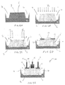
Figures 2A-2E schematically illustrate the various stages in a process flow for making an integrated circuit in accordance with an embodiment of the invention; -
Figures 3A-3F schematically illustrate the various stages in a process flow for making an integrated circuit in accordance with another embodiment of the invention; and -
Figures 4A-4E schematically illustrate the various stages in a process flow for making an integrated circuit in accordance with a further embodiment of the invention. - Embodiments of the present invention are described in the following with reference to the accompanying drawings.
- This invention can provide an integrated circuit comprising a diode, such as a Schottky diode, which can be manufactured using standard CMOS processing techniques. In particular, a diode in accordance with this invention can be manufactured as part of a middle or back end of line process flow.
- A first embodiment of a method for making an integrated circuit comprising a Schottky diode is described below in relation to
Figure 2 . - In a first stage of the method, there is provided a
semiconductor substrate 2. Thesubstrate 2 may comprise any suitable material, for example silicon.Trenches 4 are formed in a major surface of thesubstrate 2 using, for example, one or more conventional masking and etching steps. Thetrenches 4 may be filled with an insulating material. Thetrenches 4 may, for example, be shallow trench isolation (STI) trenches. - In this example, the
trenches 4 define anactive region 6 of thesubstrate 2. Theactive region 6 is bordered by thetrenches 4, which can constitute an isolation region in thesubstrate 2, isolating theactive region 6 from other parts of thesubstrate 2. In plan view, theactive region 6 bordered by thetrenches 4 may have a substantially oblong shape, although other shapes may also be used (for example, hexagonal, square, circle etc.). - Turning to
Figure 2 , following formation of thetrenches 4 to define the active region 6 a well implantation step I1 is performed, to dope theactive region 6. Either n-type or p-type doping may be used, according to design requirements for the diode. - As shown in
Figure 2c , a further implantation step I2 is then performed, to form dopedcontact implants 8. Typically, thecontact implants 8 will have a conductivity type that is the same as that of the dopedactive region 6. However, thecontact implant 8 can be doped to a higher level than the remainder of theactive region 6, thereby to enable silicidation to ensure the provision of ohmic contacts. - A protection layer 14 is then formed on the surface of the
active region 6. This layer 14 protects the surface of theactive region 6 during the subsequent silicidation step. In this example, the protection layer 14 is formed in a gap in between thecontact implants 8. The protection layer 14 may, for example, comprise a nitride layer. Thereafter, thecontact implants 8 are silicidated to form thesilicide contacts 12. - In a further step shown in
Figure 2e ,metal contacts 16 and 18 are formed. Thecontacts 18 connect to thesilicide contacts 12, while the contact 16 makes direct contact with the surface of the dopedactive region 6. The contact 16 passes through an opening provided in the protection layer 14. The opening can be formed using, for example, an etching step. - All of the method steps described above can be incorporated into standard CMOS process flows in the middle or back end of line.
- Accordingly, a diode according to an embodiment of the invention can comprise a
semiconductor substrate 2 having anactive region 6 that is bordered by an isolation region (such as the trenches 4). A first electrode 16 of the diode comprises a metal contact that is provided on a surface of theactive region 6. A second electrode of the diode comprises asilicide contact 12 that is also provided on the surface of theactive region 6. - A second embodiment of a method according to this invention is described below in relation to
Figure 3 . - As shown in
Figures 3a, 3b and 3c , the initial stages of the second embodiment are substantially the same as those described above in relation toFigures 2a, 2b and 2c . However, in this second embodiment, a third implantation step I3 is performed to form asemiconductor portion 20, which has a conductivity type which is opposite to the conductivity type of the dopedactive portion 6. Thesemiconductor portion 20 in this example is located in between thecontact implants 8. Thesemiconductor portion 20 may also have a higher doping level than the remainder of theactive region 6. - Subsequently, and as described above in relation to
Figure 2d , a protection layer 14 is formed, andsilicide contacts 12 are provided. The result of this stage is shown inFigure 3e . - Turning to
Figure 3f , it is shown thatmetal contacts 18, 16 are then provided as described above in relation toFigure 2e . In this example, the portion ofsemiconductor material 20 is provided adjacent the edges of the metal contact 16. The provision of the portion ofsemiconductor material 20 having a conductivity type opposite to that of the remainder of theactive region 6 aids in reducing leakage currents. In particular the junction between the active region 6 (which has a first conductivity type) and the portion 20 (which has a conductivity type opposite to the first conductivity type) blocks such leakage currents. The portion ofsemiconductor material 20 can substantially surround the metal contact 16 in the region at which the metal contact 16 meets the surface of theactive region 6, forming a closed ring. Moreover, the portion ofsemiconductor material 20 can overlap the edges of the metal contact 16. This enhances the ability of the portion ofsemiconductor material 20 to inhibit leakage currents, since extra leakage currents normally arise from the Schottky contact edges. - The metal contact 16 can, in accordance with an embodiment of the invention, be provided as part of an interconnect level of the integrated circuit. The interconnect level can, for example, comprise a local interconnect level (LIL) of the integrated circuit. The local interconnect level is typically provided as part of standard of back end of line processing. Since the use of metal is normally prohibited during front end of line of processing, this invention conveniently allows the formation of a metal Schottky contact, using standard CMOS processing, in which the standard local interconnect level metallisation process can be employed to provide the necessary metal contacts of the diode.
- A third embodiment of the invention is described below in relation to
Figure 4 . In this third embodiment, the initial stages are substantially the same as those described above in relation toFigures 2a to 2d . - Some back end of line process flows do not include the provision of a local interconnect level. In such examples, instead of using the local interconnect level to provide the necessary metal for the diode, a lower (for example, lowest) metal level (M1) can be used instead. This is shown in Figure 40, where the metal contacts 16 form part of the lowest metal level M1. As is shown, multiple contacts 16 may be provided, and the number of contacts is limited primarily by the amount of space that is provided on the surface of the
active region 6 in between thesilicide contacts 12. - In embodiments in which an interconnect level (for example, either a local interconnect level or a lower metal level) of the integrated circuit is used the switch output characteristics of the Schottky diode can be tailored by selecting the metal composition used for the interconnects. The metal composition of the interconnect determines the work function of the first electrode, thus influencing factors such as the switch on voltage Vf of the diode. Examples of materials that can be used for the interconnect level include Ti and Co. These can be used to form TiSi, TiSi2, and CoSi2 contacts.
- Accordingly, there has been described a diode and a method of making the same. The diode includes a semiconductor substrate having an active region bordered by an isolation region, a first electrode having a metal contact provided on a surface of the active region, and a second electrode having a silicide contact also provided on the surface of the active region.
- Although particular embodiments of the invention have been described, it will be appreciated that many modifications/additions and/or substitutions may be made within the scope of the claimed invention.
Claims (17)
- An integrated circuit including a Schottky diode, the diode comprising:an active region bordered by an isolation region in a semiconductor substrate of the integrated circuit;a first electrode comprising a metal contact provided on a surface of the active region; anda second electrode comprising a silicide contact also provided on said surface of said active region.
- The integrated circuit of claim 1, wherein the isolation region comprises shallow trench isolation.
- The integrated circuit of claim 1 or claim 2, wherein the active region comprises a doped well, and wherein the first and second electrodes are provided on the surface of the active region above the doped well.
- The integrated circuit of any preceding claim, wherein:a portion of the surface of the active region is covered by a protection layer;the metal contact extends through the protection layer to meet the surface of the active region; andthe silicide contact is provided on an exposed portion of the surface of the active region not covered by the protection layer.
- The integrated circuit of any preceding claim, comprising a portion of semiconductor material located in the active region and adjacent the edges of the metal contact of the first electrode, for reducing leakage current at said edges, wherein the portion of semiconductor material is doped to have a conductivity type opposite to that of the remainder of the active region.
- The integrated circuit of claim 5, wherein portion of semiconductor material adjacent the edges of the metal contact of the first electrode forms a closed ring around the metal contact.
- The integrated circuit of any preceding claim, wherein the metal contact of the first electrode comprises a portion of an interconnect level of the substrate.
- The integrated circuit of claim 7, wherein the interconnect level is a local interconnect level of the substrate.
- The integrated circuit of claim 7, wherein the interconnect level is a lowest metal interconnect level (M1) of the substrate.
- An RFID tag including the integrated circuit of any preceding claim.
- A method of making an integrated circuit including a Schottky diode, the method comprising:providing a semiconductor substrate;providing an isolation region in the substrate, wherein the isolation borders an active region of the substrate;forming a metal contact on a surface of the active region to provide a first electrode of the diode; andforming a silicide contact on said surface of said active region to provide a second electrode of the diode.
- The method of claim 11, comprising:covering a portion of the surface of the active region with a protection layer;forming the metal contact of the first electrode such that it extends through the protection layer to meet the surface of the active region; andforming the silicide contact on an exposed portion of the surface of the active region not covered by the protective layer of semiconductor material.
- The method of claim 11 or claim 12, comprising:forming a portion of semiconductor material in the active region corresponding to an intended configuration of the metal contact of the first electrode, wherein the portion of semiconductor material is has a conductivity type opposite to that of the remainder of the active region; andforming said metal contact such that the portion of semiconductor material is positioned adjacent the edges of the metal contact, for reducing leakage current at said edges.
- The method of any of claims 11 to 13, comprising forming an interconnect level of the substrate, wherein the metal contact of the first electrode is formed is the same processing step as the formation of the interconnect level.
- The method of claim 14, wherein the interconnect level is a local interconnect level of the substrate.
- The method of claim 14, wherein the interconnect level is a lowest metal interconnect level (M1) of the substrate.
- A method of making an RFID tag, the method including the method of any of claims 11 to 16 for making an integrated circuit of the RFID tag.
Priority Applications (3)
| Application Number | Priority Date | Filing Date | Title |
|---|---|---|---|
| EP09173771A EP2315246B1 (en) | 2009-10-22 | 2009-10-22 | Integrated circuit |
| PCT/IB2010/054770 WO2011048567A1 (en) | 2009-10-22 | 2010-10-21 | Integrated circuit |
| US13/499,805 US9287414B2 (en) | 2009-10-22 | 2010-10-21 | Integrated circuit |
Applications Claiming Priority (1)
| Application Number | Priority Date | Filing Date | Title |
|---|---|---|---|
| EP09173771A EP2315246B1 (en) | 2009-10-22 | 2009-10-22 | Integrated circuit |
Publications (2)
| Publication Number | Publication Date |
|---|---|
| EP2315246A1 true EP2315246A1 (en) | 2011-04-27 |
| EP2315246B1 EP2315246B1 (en) | 2012-07-11 |
Family
ID=41722939
Family Applications (1)
| Application Number | Title | Priority Date | Filing Date |
|---|---|---|---|
| EP09173771A Active EP2315246B1 (en) | 2009-10-22 | 2009-10-22 | Integrated circuit |
Country Status (3)
| Country | Link |
|---|---|
| US (1) | US9287414B2 (en) |
| EP (1) | EP2315246B1 (en) |
| WO (1) | WO2011048567A1 (en) |
Citations (5)
| Publication number | Priority date | Publication date | Assignee | Title |
|---|---|---|---|---|
| US5696025A (en) * | 1996-02-02 | 1997-12-09 | Micron Technology, Inc. | Method of forming guard ringed schottky diode |
| EP1229491A1 (en) * | 2001-02-02 | 2002-08-07 | Sharp Kabushiki Kaisha | Integrated semiconductor circuit device, process of manufacturing the same, ic module and ic card |
| US20070139164A1 (en) * | 1996-05-13 | 2007-06-21 | O'toole James E | Radio frequency data communications device |
| JP2008085199A (en) * | 2006-09-28 | 2008-04-10 | Sanyo Electric Co Ltd | Semiconductor device |
| WO2008107263A1 (en) | 2007-03-08 | 2008-09-12 | Austriamicrosystems Ag | Method for the production of a schottky diode and semiconductor element having a schottky diode |
Family Cites Families (6)
| Publication number | Priority date | Publication date | Assignee | Title |
|---|---|---|---|---|
| US6949454B2 (en) * | 2003-10-08 | 2005-09-27 | Texas Instruments Incorporated | Guard ring structure for a Schottky diode |
| US7544557B2 (en) * | 2004-12-15 | 2009-06-09 | Tower Semiconductor Ltd. | Gate defined Schottky diode |
| US20070052057A1 (en) * | 2005-09-07 | 2007-03-08 | Texas Instruments Incorporated | Method and Schottky diode structure for avoiding intrinsic NPM transistor operation |
| US8338906B2 (en) * | 2008-01-30 | 2012-12-25 | Taiwan Semiconductor Manufacturing Co., Ltd. | Schottky device |
| US7943472B2 (en) * | 2008-01-31 | 2011-05-17 | Texas Instruments Incorporated | CoSi2 Schottky diode integration in BiSMOS process |
| TWI383508B (en) * | 2008-12-17 | 2013-01-21 | 世界先進積體電路股份有限公司 | High voltage semiconductor component with Schottky diode |
-
2009
- 2009-10-22 EP EP09173771A patent/EP2315246B1/en active Active
-
2010
- 2010-10-21 US US13/499,805 patent/US9287414B2/en active Active
- 2010-10-21 WO PCT/IB2010/054770 patent/WO2011048567A1/en not_active Ceased
Patent Citations (5)
| Publication number | Priority date | Publication date | Assignee | Title |
|---|---|---|---|---|
| US5696025A (en) * | 1996-02-02 | 1997-12-09 | Micron Technology, Inc. | Method of forming guard ringed schottky diode |
| US20070139164A1 (en) * | 1996-05-13 | 2007-06-21 | O'toole James E | Radio frequency data communications device |
| EP1229491A1 (en) * | 2001-02-02 | 2002-08-07 | Sharp Kabushiki Kaisha | Integrated semiconductor circuit device, process of manufacturing the same, ic module and ic card |
| JP2008085199A (en) * | 2006-09-28 | 2008-04-10 | Sanyo Electric Co Ltd | Semiconductor device |
| WO2008107263A1 (en) | 2007-03-08 | 2008-09-12 | Austriamicrosystems Ag | Method for the production of a schottky diode and semiconductor element having a schottky diode |
Also Published As
| Publication number | Publication date |
|---|---|
| US20120199937A1 (en) | 2012-08-09 |
| US9287414B2 (en) | 2016-03-15 |
| WO2011048567A1 (en) | 2011-04-28 |
| EP2315246B1 (en) | 2012-07-11 |
Similar Documents
| Publication | Publication Date | Title |
|---|---|---|
| US8338906B2 (en) | Schottky device | |
| US11600615B2 (en) | Protection devices with trigger devices and methods of formation thereof | |
| US8377757B2 (en) | Device and method for transient voltage suppressor | |
| US20020177324A1 (en) | Vertical metal oxide silicon field effect semiconductor diodes | |
| US20100237414A1 (en) | MSD integrated circuits with shallow trench | |
| US10050140B2 (en) | Rectifier diode | |
| JP3983671B2 (en) | Schottky diode | |
| CN102184920A (en) | Voltage converter and system including voltage converter | |
| CN105789331B (en) | Semiconductor rectifier device and preparation method thereof | |
| US8809988B2 (en) | Low leakage and/or low turn-on voltage Schottky diode | |
| US10056260B2 (en) | Schottky diode with dielectrically isolated diffusions, and method of manufacturing the same | |
| US9406788B2 (en) | Structure of a trench MOS rectifier and method of forming the same | |
| CN101681840A (en) | Junction barrier schottky diode | |
| EP2315246B1 (en) | Integrated circuit | |
| US8709885B2 (en) | Schottky diode and method of manufacture | |
| CN109873039B (en) | Schottky diode and LDMOSFET integrated with Schottky diode | |
| US10032937B2 (en) | Monolithic series switching semiconductor device having low-resistance substrate contact structure and method | |
| US20090224355A1 (en) | Semiconductor device with buffer layer | |
| US7528459B2 (en) | Punch-through diode and method of processing the same | |
| CN105161417A (en) | Process method for Schottky barrier diode | |
| CN105932010A (en) | Transient voltage suppressor | |
| CN224234068U (en) | Schottky diode and buck converter comprising the same | |
| JP2006319096A (en) | Schottky barrier diode | |
| KR20160040926A (en) | Power semiconductor devices |
Legal Events
| Date | Code | Title | Description |
|---|---|---|---|
| PUAI | Public reference made under article 153(3) epc to a published international application that has entered the european phase |
Free format text: ORIGINAL CODE: 0009012 |
|
| AK | Designated contracting states |
Kind code of ref document: A1 Designated state(s): AT BE BG CH CY CZ DE DK EE ES FI FR GB GR HR HU IE IS IT LI LT LU LV MC MK MT NL NO PL PT RO SE SI SK SM TR |
|
| AX | Request for extension of the european patent |
Extension state: AL BA RS |
|
| 17P | Request for examination filed |
Effective date: 20110906 |
|
| RAP1 | Party data changed (applicant data changed or rights of an application transferred) |
Owner name: TAIWAN SEMICONDUCTOR MANUFACTURING CO., LTD. |
|
| REG | Reference to a national code |
Ref country code: DE Ref legal event code: R079 Ref document number: 602009008175 Country of ref document: DE Free format text: PREVIOUS MAIN CLASS: H01L0027060000 Ipc: G06K0019070000 |
|
| RIC1 | Information provided on ipc code assigned before grant |
Ipc: H01L 21/329 20060101ALI20111213BHEP Ipc: H01L 29/872 20060101ALI20111213BHEP Ipc: G06K 19/07 20060101AFI20111213BHEP |
|
| GRAP | Despatch of communication of intention to grant a patent |
Free format text: ORIGINAL CODE: EPIDOSNIGR1 |
|
| GRAS | Grant fee paid |
Free format text: ORIGINAL CODE: EPIDOSNIGR3 |
|
| GRAA | (expected) grant |
Free format text: ORIGINAL CODE: 0009210 |
|
| AK | Designated contracting states |
Kind code of ref document: B1 Designated state(s): AT BE BG CH CY CZ DE DK EE ES FI FR GB GR HR HU IE IS IT LI LT LU LV MC MK MT NL NO PL PT RO SE SI SK SM TR |
|
| REG | Reference to a national code |
Ref country code: GB Ref legal event code: FG4D |
|
| REG | Reference to a national code |
Ref country code: CH Ref legal event code: EP |
|
| REG | Reference to a national code |
Ref country code: AT Ref legal event code: REF Ref document number: 566446 Country of ref document: AT Kind code of ref document: T Effective date: 20120715 |
|
| REG | Reference to a national code |
Ref country code: IE Ref legal event code: FG4D |
|
| REG | Reference to a national code |
Ref country code: DE Ref legal event code: R096 Ref document number: 602009008175 Country of ref document: DE Effective date: 20120906 |
|
| REG | Reference to a national code |
Ref country code: NL Ref legal event code: VDEP Effective date: 20120711 |
|
| REG | Reference to a national code |
Ref country code: AT Ref legal event code: MK05 Ref document number: 566446 Country of ref document: AT Kind code of ref document: T Effective date: 20120711 |
|
| REG | Reference to a national code |
Ref country code: LT Ref legal event code: MG4D Effective date: 20120711 |
|
| PG25 | Lapsed in a contracting state [announced via postgrant information from national office to epo] |
Ref country code: BE Free format text: LAPSE BECAUSE OF FAILURE TO SUBMIT A TRANSLATION OF THE DESCRIPTION OR TO PAY THE FEE WITHIN THE PRESCRIBED TIME-LIMIT Effective date: 20120711 Ref country code: NO Free format text: LAPSE BECAUSE OF FAILURE TO SUBMIT A TRANSLATION OF THE DESCRIPTION OR TO PAY THE FEE WITHIN THE PRESCRIBED TIME-LIMIT Effective date: 20121011 Ref country code: IS Free format text: LAPSE BECAUSE OF FAILURE TO SUBMIT A TRANSLATION OF THE DESCRIPTION OR TO PAY THE FEE WITHIN THE PRESCRIBED TIME-LIMIT Effective date: 20121111 Ref country code: AT Free format text: LAPSE BECAUSE OF FAILURE TO SUBMIT A TRANSLATION OF THE DESCRIPTION OR TO PAY THE FEE WITHIN THE PRESCRIBED TIME-LIMIT Effective date: 20120711 Ref country code: HR Free format text: LAPSE BECAUSE OF FAILURE TO SUBMIT A TRANSLATION OF THE DESCRIPTION OR TO PAY THE FEE WITHIN THE PRESCRIBED TIME-LIMIT Effective date: 20120711 Ref country code: FI Free format text: LAPSE BECAUSE OF FAILURE TO SUBMIT A TRANSLATION OF THE DESCRIPTION OR TO PAY THE FEE WITHIN THE PRESCRIBED TIME-LIMIT Effective date: 20120711 Ref country code: CY Free format text: LAPSE BECAUSE OF FAILURE TO SUBMIT A TRANSLATION OF THE DESCRIPTION OR TO PAY THE FEE WITHIN THE PRESCRIBED TIME-LIMIT Effective date: 20120711 Ref country code: LT Free format text: LAPSE BECAUSE OF FAILURE TO SUBMIT A TRANSLATION OF THE DESCRIPTION OR TO PAY THE FEE WITHIN THE PRESCRIBED TIME-LIMIT Effective date: 20120711 |
|
| PG25 | Lapsed in a contracting state [announced via postgrant information from national office to epo] |
Ref country code: PL Free format text: LAPSE BECAUSE OF FAILURE TO SUBMIT A TRANSLATION OF THE DESCRIPTION OR TO PAY THE FEE WITHIN THE PRESCRIBED TIME-LIMIT Effective date: 20120711 Ref country code: SI Free format text: LAPSE BECAUSE OF FAILURE TO SUBMIT A TRANSLATION OF THE DESCRIPTION OR TO PAY THE FEE WITHIN THE PRESCRIBED TIME-LIMIT Effective date: 20120711 Ref country code: SE Free format text: LAPSE BECAUSE OF FAILURE TO SUBMIT A TRANSLATION OF THE DESCRIPTION OR TO PAY THE FEE WITHIN THE PRESCRIBED TIME-LIMIT Effective date: 20120711 Ref country code: PT Free format text: LAPSE BECAUSE OF FAILURE TO SUBMIT A TRANSLATION OF THE DESCRIPTION OR TO PAY THE FEE WITHIN THE PRESCRIBED TIME-LIMIT Effective date: 20121112 Ref country code: LV Free format text: LAPSE BECAUSE OF FAILURE TO SUBMIT A TRANSLATION OF THE DESCRIPTION OR TO PAY THE FEE WITHIN THE PRESCRIBED TIME-LIMIT Effective date: 20120711 Ref country code: GR Free format text: LAPSE BECAUSE OF FAILURE TO SUBMIT A TRANSLATION OF THE DESCRIPTION OR TO PAY THE FEE WITHIN THE PRESCRIBED TIME-LIMIT Effective date: 20121012 |
|
| PG25 | Lapsed in a contracting state [announced via postgrant information from national office to epo] |
Ref country code: NL Free format text: LAPSE BECAUSE OF FAILURE TO SUBMIT A TRANSLATION OF THE DESCRIPTION OR TO PAY THE FEE WITHIN THE PRESCRIBED TIME-LIMIT Effective date: 20120711 |
|
| PG25 | Lapsed in a contracting state [announced via postgrant information from national office to epo] |
Ref country code: ES Free format text: LAPSE BECAUSE OF FAILURE TO SUBMIT A TRANSLATION OF THE DESCRIPTION OR TO PAY THE FEE WITHIN THE PRESCRIBED TIME-LIMIT Effective date: 20121022 Ref country code: RO Free format text: LAPSE BECAUSE OF FAILURE TO SUBMIT A TRANSLATION OF THE DESCRIPTION OR TO PAY THE FEE WITHIN THE PRESCRIBED TIME-LIMIT Effective date: 20120711 Ref country code: CZ Free format text: LAPSE BECAUSE OF FAILURE TO SUBMIT A TRANSLATION OF THE DESCRIPTION OR TO PAY THE FEE WITHIN THE PRESCRIBED TIME-LIMIT Effective date: 20120711 Ref country code: DK Free format text: LAPSE BECAUSE OF FAILURE TO SUBMIT A TRANSLATION OF THE DESCRIPTION OR TO PAY THE FEE WITHIN THE PRESCRIBED TIME-LIMIT Effective date: 20120711 Ref country code: EE Free format text: LAPSE BECAUSE OF FAILURE TO SUBMIT A TRANSLATION OF THE DESCRIPTION OR TO PAY THE FEE WITHIN THE PRESCRIBED TIME-LIMIT Effective date: 20120711 |
|
| PLBE | No opposition filed within time limit |
Free format text: ORIGINAL CODE: 0009261 |
|
| STAA | Information on the status of an ep patent application or granted ep patent |
Free format text: STATUS: NO OPPOSITION FILED WITHIN TIME LIMIT |
|
| PG25 | Lapsed in a contracting state [announced via postgrant information from national office to epo] |
Ref country code: MC Free format text: LAPSE BECAUSE OF NON-PAYMENT OF DUE FEES Effective date: 20121031 Ref country code: IT Free format text: LAPSE BECAUSE OF FAILURE TO SUBMIT A TRANSLATION OF THE DESCRIPTION OR TO PAY THE FEE WITHIN THE PRESCRIBED TIME-LIMIT Effective date: 20120711 Ref country code: SK Free format text: LAPSE BECAUSE OF FAILURE TO SUBMIT A TRANSLATION OF THE DESCRIPTION OR TO PAY THE FEE WITHIN THE PRESCRIBED TIME-LIMIT Effective date: 20120711 |
|
| 26N | No opposition filed |
Effective date: 20130412 |
|
| REG | Reference to a national code |
Ref country code: IE Ref legal event code: MM4A |
|
| REG | Reference to a national code |
Ref country code: FR Ref legal event code: ST Effective date: 20130628 |
|
| PG25 | Lapsed in a contracting state [announced via postgrant information from national office to epo] |
Ref country code: IE Free format text: LAPSE BECAUSE OF NON-PAYMENT OF DUE FEES Effective date: 20121022 Ref country code: BG Free format text: LAPSE BECAUSE OF FAILURE TO SUBMIT A TRANSLATION OF THE DESCRIPTION OR TO PAY THE FEE WITHIN THE PRESCRIBED TIME-LIMIT Effective date: 20121011 |
|
| REG | Reference to a national code |
Ref country code: DE Ref legal event code: R097 Ref document number: 602009008175 Country of ref document: DE Effective date: 20130412 |
|
| PG25 | Lapsed in a contracting state [announced via postgrant information from national office to epo] |
Ref country code: FR Free format text: LAPSE BECAUSE OF NON-PAYMENT OF DUE FEES Effective date: 20121031 |
|
| PG25 | Lapsed in a contracting state [announced via postgrant information from national office to epo] |
Ref country code: MT Free format text: LAPSE BECAUSE OF FAILURE TO SUBMIT A TRANSLATION OF THE DESCRIPTION OR TO PAY THE FEE WITHIN THE PRESCRIBED TIME-LIMIT Effective date: 20120711 |
|
| PG25 | Lapsed in a contracting state [announced via postgrant information from national office to epo] |
Ref country code: TR Free format text: LAPSE BECAUSE OF FAILURE TO SUBMIT A TRANSLATION OF THE DESCRIPTION OR TO PAY THE FEE WITHIN THE PRESCRIBED TIME-LIMIT Effective date: 20120711 |
|
| PG25 | Lapsed in a contracting state [announced via postgrant information from national office to epo] |
Ref country code: LU Free format text: LAPSE BECAUSE OF NON-PAYMENT OF DUE FEES Effective date: 20121022 Ref country code: SM Free format text: LAPSE BECAUSE OF FAILURE TO SUBMIT A TRANSLATION OF THE DESCRIPTION OR TO PAY THE FEE WITHIN THE PRESCRIBED TIME-LIMIT Effective date: 20120711 |
|
| REG | Reference to a national code |
Ref country code: CH Ref legal event code: PL |
|
| GBPC | Gb: european patent ceased through non-payment of renewal fee |
Effective date: 20131022 |
|
| PG25 | Lapsed in a contracting state [announced via postgrant information from national office to epo] |
Ref country code: CH Free format text: LAPSE BECAUSE OF NON-PAYMENT OF DUE FEES Effective date: 20131031 Ref country code: GB Free format text: LAPSE BECAUSE OF NON-PAYMENT OF DUE FEES Effective date: 20131022 Ref country code: HU Free format text: LAPSE BECAUSE OF FAILURE TO SUBMIT A TRANSLATION OF THE DESCRIPTION OR TO PAY THE FEE WITHIN THE PRESCRIBED TIME-LIMIT Effective date: 20091022 Ref country code: LI Free format text: LAPSE BECAUSE OF NON-PAYMENT OF DUE FEES Effective date: 20131031 |
|
| PG25 | Lapsed in a contracting state [announced via postgrant information from national office to epo] |
Ref country code: MK Free format text: LAPSE BECAUSE OF FAILURE TO SUBMIT A TRANSLATION OF THE DESCRIPTION OR TO PAY THE FEE WITHIN THE PRESCRIBED TIME-LIMIT Effective date: 20120711 |
|
| PGFP | Annual fee paid to national office [announced via postgrant information from national office to epo] |
Ref country code: DE Payment date: 20251029 Year of fee payment: 17 |