EP2312385B1 - Liquid crystal panel and liquid crystal display device - Google Patents
Liquid crystal panel and liquid crystal display device Download PDFInfo
- Publication number
- EP2312385B1 EP2312385B1 EP09766706.7A EP09766706A EP2312385B1 EP 2312385 B1 EP2312385 B1 EP 2312385B1 EP 09766706 A EP09766706 A EP 09766706A EP 2312385 B1 EP2312385 B1 EP 2312385B1
- Authority
- EP
- European Patent Office
- Prior art keywords
- liquid crystal
- substrate
- electrode
- crystal material
- crystal panel
- Prior art date
- Legal status (The legal status is an assumption and is not a legal conclusion. Google has not performed a legal analysis and makes no representation as to the accuracy of the status listed.)
- Active
Links
Images


Classifications
-
- G—PHYSICS
- G02—OPTICS
- G02F—OPTICAL DEVICES OR ARRANGEMENTS FOR THE CONTROL OF LIGHT BY MODIFICATION OF THE OPTICAL PROPERTIES OF THE MEDIA OF THE ELEMENTS INVOLVED THEREIN; NON-LINEAR OPTICS; FREQUENCY-CHANGING OF LIGHT; OPTICAL LOGIC ELEMENTS; OPTICAL ANALOGUE/DIGITAL CONVERTERS
- G02F1/00—Devices or arrangements for the control of the intensity, colour, phase, polarisation or direction of light arriving from an independent light source, e.g. switching, gating or modulating; Non-linear optics
- G02F1/01—Devices or arrangements for the control of the intensity, colour, phase, polarisation or direction of light arriving from an independent light source, e.g. switching, gating or modulating; Non-linear optics for the control of the intensity, phase, polarisation or colour
- G02F1/13—Devices or arrangements for the control of the intensity, colour, phase, polarisation or direction of light arriving from an independent light source, e.g. switching, gating or modulating; Non-linear optics for the control of the intensity, phase, polarisation or colour based on liquid crystals, e.g. single liquid crystal display cells
- G02F1/133—Constructional arrangements; Operation of liquid crystal cells; Circuit arrangements
- G02F1/1333—Constructional arrangements; Manufacturing methods
- G02F1/1343—Electrodes
- G02F1/134309—Electrodes characterised by their geometrical arrangement
- G02F1/134363—Electrodes characterised by their geometrical arrangement for applying an electric field parallel to the substrate, i.e. in-plane switching [IPS]
-
- G—PHYSICS
- G02—OPTICS
- G02F—OPTICAL DEVICES OR ARRANGEMENTS FOR THE CONTROL OF LIGHT BY MODIFICATION OF THE OPTICAL PROPERTIES OF THE MEDIA OF THE ELEMENTS INVOLVED THEREIN; NON-LINEAR OPTICS; FREQUENCY-CHANGING OF LIGHT; OPTICAL LOGIC ELEMENTS; OPTICAL ANALOGUE/DIGITAL CONVERTERS
- G02F1/00—Devices or arrangements for the control of the intensity, colour, phase, polarisation or direction of light arriving from an independent light source, e.g. switching, gating or modulating; Non-linear optics
- G02F1/01—Devices or arrangements for the control of the intensity, colour, phase, polarisation or direction of light arriving from an independent light source, e.g. switching, gating or modulating; Non-linear optics for the control of the intensity, phase, polarisation or colour
- G02F1/13—Devices or arrangements for the control of the intensity, colour, phase, polarisation or direction of light arriving from an independent light source, e.g. switching, gating or modulating; Non-linear optics for the control of the intensity, phase, polarisation or colour based on liquid crystals, e.g. single liquid crystal display cells
- G02F1/137—Devices or arrangements for the control of the intensity, colour, phase, polarisation or direction of light arriving from an independent light source, e.g. switching, gating or modulating; Non-linear optics for the control of the intensity, phase, polarisation or colour based on liquid crystals, e.g. single liquid crystal display cells characterised by the electro-optical or magneto-optical effect, e.g. field-induced phase transition, orientation effect, guest-host interaction or dynamic scattering
- G02F1/139—Devices or arrangements for the control of the intensity, colour, phase, polarisation or direction of light arriving from an independent light source, e.g. switching, gating or modulating; Non-linear optics for the control of the intensity, phase, polarisation or colour based on liquid crystals, e.g. single liquid crystal display cells characterised by the electro-optical or magneto-optical effect, e.g. field-induced phase transition, orientation effect, guest-host interaction or dynamic scattering based on orientation effects in which the liquid crystal remains transparent
- G02F1/1393—Devices or arrangements for the control of the intensity, colour, phase, polarisation or direction of light arriving from an independent light source, e.g. switching, gating or modulating; Non-linear optics for the control of the intensity, phase, polarisation or colour based on liquid crystals, e.g. single liquid crystal display cells characterised by the electro-optical or magneto-optical effect, e.g. field-induced phase transition, orientation effect, guest-host interaction or dynamic scattering based on orientation effects in which the liquid crystal remains transparent the birefringence of the liquid crystal being electrically controlled, e.g. ECB-, DAP-, HAN-, PI-LC cells
- G02F1/1395—Optically compensated birefringence [OCB]- cells or PI- cells
-
- G—PHYSICS
- G02—OPTICS
- G02F—OPTICAL DEVICES OR ARRANGEMENTS FOR THE CONTROL OF LIGHT BY MODIFICATION OF THE OPTICAL PROPERTIES OF THE MEDIA OF THE ELEMENTS INVOLVED THEREIN; NON-LINEAR OPTICS; FREQUENCY-CHANGING OF LIGHT; OPTICAL LOGIC ELEMENTS; OPTICAL ANALOGUE/DIGITAL CONVERTERS
- G02F1/00—Devices or arrangements for the control of the intensity, colour, phase, polarisation or direction of light arriving from an independent light source, e.g. switching, gating or modulating; Non-linear optics
- G02F1/01—Devices or arrangements for the control of the intensity, colour, phase, polarisation or direction of light arriving from an independent light source, e.g. switching, gating or modulating; Non-linear optics for the control of the intensity, phase, polarisation or colour
- G02F1/13—Devices or arrangements for the control of the intensity, colour, phase, polarisation or direction of light arriving from an independent light source, e.g. switching, gating or modulating; Non-linear optics for the control of the intensity, phase, polarisation or colour based on liquid crystals, e.g. single liquid crystal display cells
- G02F1/133—Constructional arrangements; Operation of liquid crystal cells; Circuit arrangements
- G02F1/1333—Constructional arrangements; Manufacturing methods
- G02F1/1337—Surface-induced orientation of the liquid crystal molecules, e.g. by alignment layers
- G02F1/133742—Surface-induced orientation of the liquid crystal molecules, e.g. by alignment layers for homeotropic alignment
-
- G—PHYSICS
- G02—OPTICS
- G02F—OPTICAL DEVICES OR ARRANGEMENTS FOR THE CONTROL OF LIGHT BY MODIFICATION OF THE OPTICAL PROPERTIES OF THE MEDIA OF THE ELEMENTS INVOLVED THEREIN; NON-LINEAR OPTICS; FREQUENCY-CHANGING OF LIGHT; OPTICAL LOGIC ELEMENTS; OPTICAL ANALOGUE/DIGITAL CONVERTERS
- G02F1/00—Devices or arrangements for the control of the intensity, colour, phase, polarisation or direction of light arriving from an independent light source, e.g. switching, gating or modulating; Non-linear optics
- G02F1/01—Devices or arrangements for the control of the intensity, colour, phase, polarisation or direction of light arriving from an independent light source, e.g. switching, gating or modulating; Non-linear optics for the control of the intensity, phase, polarisation or colour
- G02F1/13—Devices or arrangements for the control of the intensity, colour, phase, polarisation or direction of light arriving from an independent light source, e.g. switching, gating or modulating; Non-linear optics for the control of the intensity, phase, polarisation or colour based on liquid crystals, e.g. single liquid crystal display cells
- G02F1/137—Devices or arrangements for the control of the intensity, colour, phase, polarisation or direction of light arriving from an independent light source, e.g. switching, gating or modulating; Non-linear optics for the control of the intensity, phase, polarisation or colour based on liquid crystals, e.g. single liquid crystal display cells characterised by the electro-optical or magneto-optical effect, e.g. field-induced phase transition, orientation effect, guest-host interaction or dynamic scattering
- G02F1/13706—Devices or arrangements for the control of the intensity, colour, phase, polarisation or direction of light arriving from an independent light source, e.g. switching, gating or modulating; Non-linear optics for the control of the intensity, phase, polarisation or colour based on liquid crystals, e.g. single liquid crystal display cells characterised by the electro-optical or magneto-optical effect, e.g. field-induced phase transition, orientation effect, guest-host interaction or dynamic scattering the liquid crystal having positive dielectric anisotropy
-
- G—PHYSICS
- G02—OPTICS
- G02F—OPTICAL DEVICES OR ARRANGEMENTS FOR THE CONTROL OF LIGHT BY MODIFICATION OF THE OPTICAL PROPERTIES OF THE MEDIA OF THE ELEMENTS INVOLVED THEREIN; NON-LINEAR OPTICS; FREQUENCY-CHANGING OF LIGHT; OPTICAL LOGIC ELEMENTS; OPTICAL ANALOGUE/DIGITAL CONVERTERS
- G02F2201/00—Constructional arrangements not provided for in groups G02F1/00 - G02F7/00
- G02F2201/12—Constructional arrangements not provided for in groups G02F1/00 - G02F7/00 electrode
- G02F2201/124—Constructional arrangements not provided for in groups G02F1/00 - G02F7/00 electrode interdigital
Definitions
- the present invention relates to a liquid crystal panel and a liquid crystal display device, in particular, to a liquid crystal display panel and a liquid crystal display device each controlling transmission of light by causing bend distortion of a liquid crystal layer by voltage application.
- Liquid crystal display devices have a small thickness, a light weight, and a low power consumption as characteristics, and are used in various fields. Display performance of such liquid crystal display devices is drastically improved year by year. As a result, recently the display performance of liquid crystal display devices has become superior to that of CRTs (cathode ray tubes).
- a display mode of a liquid crystal display device is determined by how liquid crystal is aligned in a liquid crystal cell.
- various display modes are known as display modes of liquid crystal display devices. Examples of such display modes known are a TN (Twisted Nematic) mode, an MVA (Multi-domain Vertical Alignment) mode, an IPS (In-Plain Switching) mode, and an OCB (Optically Compensated Birefringence) mode. Liquid crystal display devices employing these display methods have been mass-produced conventionally.
- the fast response is realized by a three-electrode structure that can produce an electric field horizontally and vertically, alternately to turn the liquid crystal cell on and off so that both the turn-on and turn-off processes are driven by the electric field.
- the response time, transmittance-voltage curve, and the bias effect were characterized for cells with various stripe widths/gaps.
- a simple theoretical model was used to explain the bias voltage dependence of the transmission with good agreement with the experimental findings.
- a total response time (rise-time plus fall-time) of 1.88 ms was obtained.
- liquid crystal display devices of these various display modes for example, a liquid crystal display device employing the TN mode is generally used in a wide range.
- a liquid crystal display device employing the TN mode has disadvantages such as a slow response and a narrow viewing angle.
- the MVA mode (Refer to, for example, Non Patent Literatures 1 and 2) is a display mode according to which a fringe field is formed by providing a slit to each pixel electrode on an active matrix substrate and, further, providing a rib for controlling liquid crystal molecule alignment to a counter electrode on a counter substrate, thereby providing a plurality of alignment directions of liquid crystal molecules.
- the MVA mode liquid crystal display device achieves a wide viewing angle by having a plurality of divisional directions (Multi-domains) in each of which liquid crystal molecules are tilted at the time when a voltage is applied. Further, employing a vertical alignment mode, the MVA mode liquid crystal display device can obtain a higher contrast as compared with liquid crystal display devices of other modes such as the TN mode, the IPS mode, and the OCB mode.
- the MVA mode liquid crystal display has disadvantages such that (i) a production process is complex and (ii) as with the TN mode liquid crystal display device, a response speed is slow.
- the IPS mode (Refer, for example, to Non Patent Literatures 3 and 4) is known as a display mode according to which a wide viewing angle is achieved by using a simpler configuration. Switching the liquid crystal molecules within a plane, the IPS mode liquid crystal display device has a very wide viewing angle.
- the IPS mode also has a disadvantage such that a response speed is slow as with the TN mode and the MVA mode. Further, the IPS mode is not suitable for mobile devices or in-vehicle devices for which a high speed at a low temperature is required.
- the OCB mode (Refer, for example, to Non Patent Literatures 5 and 6) is an only display mode that can achieve a high-speed response by using a simple configuration in which a nematic liquid crystal is merely sandwiched by two substrates having been subjected to alignment treatment in parallel directions. Therefore, the OCB mode is particularly spotlighted for in-vehicle applications in which a response characteristic at a low temperature may become a problem.
- the OCB mode requires a transition operation from a splay alignment that is an initial alignment to a bend alignment in driving when power supply is turned on. Accordingly, the OCB mode requires an initial transition driving circuit in addition to an ordinary driving circuit. Therefore, a factor to increase cost is inherent in the OCB mode. Further, the OCB mode is inferior in a viewing angle characteristic to the MVA mode and IPS mode.
- This display mode carries out driving by a lateral electric field in a vertical alignment mode, employing a p-type nematic liquid crystal as a liquid crystal material (Refer to, for example, Patent Literatures 1 to 6).
- the display mode while a high contrast characteristic due to vertical alignment is maintained, driving is carried out by using a lateral electric field so that an alignment direction of liquid crystal molecules is defined.
- a pixel configuration is simple because alignment control by a rib as in the MVA mode is not necessary. Further, the display mode has an excellent viewing angle characteristic.
- Patent Literatures 3 and 4 disclose that: a bent electric field is formed by electric field application; two domains having liquid crystal directors in directions different from each other by 180 degrees are formed; and, as a result, a wide viewing angle is obtained.
- the display mode described above has a serious problem such that a driving voltage is high and a light transmittance is low, though having a high contrast and an excellent viewing angle characteristic as described above. Further, as in the MVA mode, a response characteristic of the display mode is not sufficient for moving image display. Therefore, this display mode has not been put to practical use yet.
- An object of the present invention is to provide a practical liquid crystal panel and a practical liquid crystal display device each of which is capable of simultaneously achieving characteristics of a high-speed response, a wide viewing angle, and a high contrast.
- a degree of bend alignment (a degree of bending of p-type liquid crystal molecules in bend alignment) can be controlled by setting, to appropriate conditions, a panel configuration and physical property values of a liquid crystal material and (ii) a high light transmittance can be obtained by a practical driving voltage, by controlling the degree of bend alignment.
- a high light transmittance could be first obtained by using a practical driving voltage.
- a liquid crystal panel of the present invention includes: a liquid crystal material sandwiched by a pair of substrates; and electrodes for applying, to the liquid crystal material, an electric field parallel to a substrate surface, the liquid crystal material including a p-type liquid crystal material, the p-type liquid crystal material being vertically aligned with respect to the substrate surface at the time when no electric field is applied, the electrodes having an electrode width of 5 ⁇ m or less and an electrode spacing of 15 ⁇ m or less, the p-type liquid crystal material having, in a range of 1.3 to 3.1, a product ( ⁇ ⁇ ⁇ n) of a dielectric constant anisotropy ⁇ and a refractive index anisotropy ⁇ n, wherein the liquid crystal material includes tetracyclic liquid crystal material in a range of 15% by weight or more and 25% by weight or less.
- applying an electric field parallel to a substrate surface means “applying an electric field that at least includes a component parallel to a substrate surface”.
- the p-type liquid crystal material being vertically aligned with respect to the substrate surface means “the p-type liquid crystal material at least including an alignment component vertical with respect to the substrate surface”.
- parallel and vertical includes “substantially parallel” and “substantially vertical”.
- the liquid crystal panel is driven by a so-called lateral electric field that is parallel to the substrate surface, while a high contrast characteristic due to vertical alignment is maintained. This makes it possible to achieve a wide viewing angle characteristic and a high contrast characteristic by a simple pixel configuration. Moreover, because an initial bend transition operation is unnecessary, practical bend alignment can be achieved.
- liquid crystal panel As in a case of an OCB mode, when liquid crystal molecules are to move, liquid crystal molecule flows operate in a direction assisting the movement of the liquid crystal molecules. Therefore, a high-speed response becomes possible.
- a characteristic of such a high-speed response corresponds to a degree of bend alignment.
- the degree of bend alignment depends on physical properties (in particular ⁇ ⁇ ⁇ n) of the liquid crystal material.
- the degree of bend alignment also varies in accordance with the electrode width and the electrode spacing of the electrodes. By setting the values of the electrode width and the electrode spacing within the above range, it becomes possible to obtain a liquid crystal panel in which a degree of deformation of the liquid crystal alignment is greater than that of a conventional configuration.
- a high transmittance can be obtained by a practical driving voltage.
- the ⁇ ⁇ ⁇ n to be in a range of 1.3 to 3.1, a high transmittance and a characteristic of a high-speed response can be obtained practically. Therefore, according to the above configuration, it becomes possible to provide a practical liquid crystal panel capable of simultaneously achieving characteristics of (i) a wide viewing angle equivalent to those of an MVA mode and an IPS mode, (ii) a high-speed response as fast as or faster than that of the OCB mode, and (iii) a high contrast.
- liquid crystal panel is a liquid crystal panel where: the p-type liquid crystal material is a p-type nematic liquid crystal material; the electrodes are comb electrodes provided on at least one substrate of the pair of substrates; and the p-type nematic liquid crystal material is arranged in homeotropic alignment at the time when no electric field is applied.
- the p-type liquid crystal material is a p-type nematic liquid crystal material
- the electrodes are comb electrodes provided on at least one substrate of the pair of substrates
- the p-type nematic liquid crystal material is arranged in homeotropic alignment at the time when no electric field is applied.
- the electrodes are provided on one substrate out of the pair of substrates and an electrode film that covers all over a display area is provided on the other substrate.
- the electrode film that covers all over the display area is provided on the substrate opposing to the substrate provided with the electrode for applying, to the liquid crystal material, an electric field parallel to the substrate surface. This makes it possible to improve the voltage-transmittance characteristic as compared with a case where the electrode film is not provided. Therefore, according to the configuration above, the same transmittance as a transmittance in a case where the electrode film is not provided can be obtained at a voltage lower than a voltage in the case where the electrode film is not provided.
- a liquid crystal display device of the present invention includes the liquid crystal panel of the present invention.
- the present invention makes it possible to provide a practical display device capable of simultaneously achieving characteristics of a high-speed response, a wide viewing angle, and a high contrast.
- each of the liquid crystal panel and the liquid crystal display device of the present invention carries out driving by a so-called lateral electric field that is parallel to the substrate surface while maintaining a high contrast due to the vertical alignment. This makes it possible to achieve a wide viewing angle characteristic and a high contrast characteristic in a simple pixel configuration. Further, because an initial bend transition operation is unnecessary, practical bend alignment can be achieved.
- the liquid crystal panel and the liquid crystal display device are configured to have electrodes whose electrode width is set to 5 ⁇ m or less and electrode spacing is set to 15 ⁇ m or less, a high transmittance can be obtained by a practical driving voltage. Further, by setting the ⁇ ⁇ ⁇ n to be in a range of 1.3 to 3.1, a high transmittance and a high-speed response can be obtained practically. Therefore, according to the present invention, it is possible to provide a practical liquid crystal panel capable of simultaneously achieving characteristics of (i) a wide viewing angle equivalent to that of an MVA mode or an IPS mode, (ii) a high-speed response as fast as or faster than that of an OCB mode, and (ii) a high contrast.
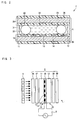
- Fig. 3 is an exploded cross sectional view schematically illustrating an outline configuration of a liquid crystal display device according to the present embodiment.
- a liquid crystal display device 1 of the present embodiment includes a liquid crystal panel 2, a driving circuit 3, and a backlight 4 (illumination device).
- Configurations of the driving circuit 3 and the backlight 4 are the same as configurations of conventional driving circuit and backlight, and explanations thereof are omitted.
- Figs. 1 and 2 show a typical panel configuration as one example of the liquid crystal panel 2 according to the present embodiment.
- Fig. 1 is an exploded perspective view schematically illustrating an outline configuration of a substantial part of the liquid crystal panel 2.
- Fig. 2 is a cross sectional view schematically illustrating an outline configuration of a substantial part of the liquid crystal panel 2.
- a substrate on a display surface side (a substrate on a side where a viewer is present) is an upper substrate and the other substrate is a lower substrate.
- the liquid crystal panel 2 of the present embodiment includes a pair of substrates 10 and 20 provided as an electrode substrate (array substrate, element substrate) and a counter substrate, so as to be opposed to each other.
- the pair of substrates 10 and 20 sandwich a liquid crystal layer 30 that is provided as a medium layer for display and that includes a p-type liquid crystal material.
- At least one of the pair of substrates 10 and 20 includes a transparent substrate such as a glass substrate. Further, one surface of the substrate 10 which surface is opposed to the substrate 20 is provided with an alignment film 12 that is a so-called vertical alignment film, and one surface of the substrate 20 which surface is opposed to the substrate 10 is provided with an alignment film 22 that is also a so-called vertical alignment film.
- the vertical alignment film is an alignment film that aligns, vertically with respect to a substrate surface, liquid crystal molecules of a liquid crystal layer, when no electric filed is applied. Note that meaning of the term “vertically” includes “substantially vertically”. Accordingly, as illustrated in Fig. 1 , p-type liquid crystal molecules 31 of the liquid crystal layer 30 exhibit homeotropic alignment, when no voltage is applied.
- one of the substrates 10 and 20 includes electric field application means to apply, to the liquid crystal layer 30, an electric field that is parallel to the substrate surface.
- This electric field is a so-called lateral electric field. Note that meaning of the term “parallel” above includes “substantially parallel”.
- the substrate 10 includes the glass substrate 11, and the substrate 20 includes the glass substrate 21.
- a pair of comb electrodes 13 and 14 (pixel electrode and common electrode) is provided as the electric field application means.
- the comb electrodes 13 and 14 may be made of a transparent electrode material such as ITO (Indium Tin Oxide) or metal such as aluminum. A material of the comb electrodes 13 and 14 are not specifically limited.
- the alignment film 12 is provided so as to cover the comb electrodes 13 and 14. Note that a material of the alignment films 12 and 22 and a method of forming the alignment films 12 and 22 are not specifically limited.
- the alignment films 12 and 22 may be formed by, for example, applying a known alignment film material having a vertical alignment regulating function on the comb electrodes 13 and 14.
- the electrode substrate and the counter substrate may be made of, for example, an array substrate such as a TFT array substrate and a color filter substrate.
- the electrode substrate and the counter substrate are not limited to these.
- a polarizer 35 is provided on an opposite surface of the substrate 10 with respect to the surface which faces the liquid crystal layer 30, and a polarizer 36 is provided on an opposite surface of the substrate 20 with respect to the surface which surface faces the liquid crystal layer 30.
- a wave plate 37 is provided between the substrate 10 and the polarizer 35 and a wave plate 38 is provided between the substrate 20 and the polarizer 36.
- the wave plate 37 or 38 may be provided only to one surface of the liquid crystal panel 2. In the case of a display device utilizing only transmitted light from a front surface, the wave plates 37 and 38 are dispensable.
- a liquid crystal cell 5 of the liquid crystal panel 2 is formed by, for example, as shown in Fig. 2, (i) bonding the substrate 10 to the substrate 20 via a spacer 33 by use of a sealing agent 34 and (ii) filling and sealing a medium containing the p-type liquid crystal material as a liquid crystal material in a space between the substrates 10 and 20.
- a sealing agent 34 for example, a sealing agent for bonding the substrate 10 to the substrate 20 via a spacer 33 by use of a sealing agent 34 and (ii) filling and sealing a medium containing the p-type liquid crystal material as a liquid crystal material in a space between the substrates 10 and 20.
- An example of the p-type liquid crystal material is a p-type nematic liquid crystal material.
- the liquid crystal panel 2 is formed by bonding, to the liquid crystal cell 5, the wave plates 37 and 38 and the polarizers 35 and 36 as described above.
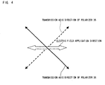
- Fig. 4 shows a relation of transmission axis directions of the polarizers 35 and 36 and an electric field application direction.
- the polarizers 35 and 36 are provided so that the transmission axis directions of the polarizers 35 and 36 are orthogonal and an angle between each of the transmission axis directions and the electric field application direction is 45 degrees.
- FIG. 5 shows, by directions of liquid crystal directors, states of rotation of the p-type liquid crystal molecules 31 due to electric field application.
- (a) of Fig. 5 is a perspective view of a substantial part of the liquid crystal panel 2 at the time when no electric field is applied.
- (b) of Fig. 5 is a perspective view of the substantial part of the liquid crystal at the time when an electric field is applied.
- the present mode is one type of display modes according to which an electric field parallel to the substrate surface is applied by use of the comb electrodes 13 and 14.
- the p-type liquid crystal molecules 31 are aligned vertically with respect to the substrate surface.
- an electric flux line is bent so as to form a semicircle.
- the p-type liquid crystal molecules 31 are arranged, in bend alignment, in an arc in a substrate thickness direction.
- the p-type liquid crystal molecules 31 show birefringence with respect to light traveling in a direction perpendicular to the substrate surface.
- the present mode while a high contrast due to the vertical alignment is maintained, driving with the use of a lateral electric field is carried out so that a direction in which the p-type liquid crystal molecules 31 are aligned is defined. Accordingly, it is not necessary to control alignment by using a rib as in an MVA mode. Further, the present mode has an excellent viewing angle characteristic in a simple pixel configuration.
- a bent electric filed (an arc electric field) is formed due to electric field application and two domains having director directions different by 180 degrees from each other are formed. As a result, a wide viewing angle characteristic can be obtained.
- the present invention is achieved based on the finding that a degree of bend alignment can be controlled unconstrainedly by changing a panel configuration and physical properties of a liquid crystal material to be used.
- the "degree of the bend alignment” means how much the p-type liquid crystal molecules 31 arranged in the bend alignment as shown in (b) of Fig. 5 are bent (hereinafter, referred to as a "curvature").
- the degree of bend alignment can be increased so that a high light transmittance can be obtained. Further, according to the present invention, because, as described above, the degree of bend alignment can be controlled unconstrainedly, a high-speed response characteristic can be achieved by utilizing a flow effect as in an OCB mode. Accordingly, the present invention has a very high practical value.
- transition from splay alignment to bend alignment occurs at a voltage a little higher than a critical driving voltage.
- the bend alignment at this time shows a maximum curvature. Therefore, in the OCB mode, gray scale display is carried out between the bend alignment showing the maximum curvature and bend alignment having gentle bending at the time when a high voltage is applied.
- gray scale display is carried out between (i) bend alignment having a large curvature at the time when a high voltage is applied and (ii) vertical alignment at the time when no voltage is applied.
- the maximum curvature depends on an applied voltage. The larger the electric field intensity becomes, the larger the maximum curvature becomes. That is, the degree of bend alignment and the maximum curvature can be controlled unconstrainedly through an electrode width L, an electrode spacing (distance between electrodes) S, and a cell gap (layer thickness of the liquid crystal material, thickness of the liquid crystal layer 30) d.
- the present mode can have a maximum curvature equal to or larger than that of the OCB mode. This makes it possible to achieve a high-speed response that is equal to or faster than that of the OCB mode.
- Fig. 6 shows equipotential curves of the liquid crystal cell 5 at the time when a voltage of 7V is applied to the liquid crystal cell 5.
- the liquid crystal cell 5 has an electrode width L of 3 ⁇ m and an electrode spacing S of 4 ⁇ m of the comb electrodes 13 and 14, and a cell gap d of 4 ⁇ m. That is, Fig. 6 shows equipotential curves of the liquid crystal cell 5 at the time when the voltage (rectangular pulse) of 7V is applied between the comb electrodes 13 and 14.
- the p-type liquid crystal molecules 31 are aligned in accordance with binding force from an interface and electric field intensity distribution shown by the equipotential curves.
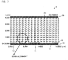
- Fig. 7 shows director distribution of the p-type liquid crystal molecules 31 in the liquid crystal cell 5 in this case. Due to voltage application, the liquid crystal molecules 31 continuously transit from the homeotropic alignment to the bend alignment. That is, in normal driving, a liquid crystal layer 30 always exhibits the bend alignment and a high-speed response can be achieved in a response from gray scale level to another gray scale level.
- Fig. 7 illustrates that, in a region where the comb electrodes 13 and 14 are not present rather than a region above the comb electrodes 13 and 14, a degree of bend distortion is greater and an optical modulation factor is larger. The following examines this in more detail.
- Fig. 8 illustrates director distribution of the liquid crystal cell 5 at the time when a voltage of 3.5V is applied to the liquid crystal cell 5.
- the liquid crystal cell 5 has an electrode width L of 2.6 ⁇ m and an electrode spacing S of 7.8 ⁇ m of the comb electrodes 13 and 14, and a cell gap d of 4 ⁇ m.
- the p-type liquid crystal material that is used has a dielectric constant anisotropy ( ⁇ ) of 20.8 and a refractive index anisotropy ( ⁇ n) of 0.14.
- the present mode is significantly different from other display modes such as an IPS mode and the OCB mode according to each of which an electric field parallel to a substrate surface is applied.
- the difference is such that, as shown in Fig. 8 , in the present mode, the p-type liquid crystal molecules 31 are always vertically aligned in regions at a center of each electrode and at a center between electrodes.
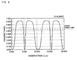
- Fig. 9 illustrates transmittance distribution in the liquid crystal cell 5 at the time when a voltage of 6V is applied to the liquid crystal cell 5 used in Fig. 8 .
- Fig. 9 illustrates the transmittance distribution in a region corresponding to the region shown in Fig. 8 . Note that each of diagrams and tables below shows transmittance on an assumption that a transmittance of 100% is an optical transmittance of the liquid crystal panel 2 at the time when no voltage is applied and that the transmittance of 100% is 1 (reference).
- a transmittance of 90 % or more can be obtained depending on a position in the liquid crystal cell 5.
- light does not transmit through regions at the center of each electrode and at the center between electrodes. Therefore, the liquid crystal cell 5 as a whole provides a transmittance of only 65% approximately.
- Fig. 11 is a graph illustrating transmittance distribution and phase difference distribution in the liquid crystal cell 5 which are measured under the same condition as the case in Fig. 10 except that the electrode spacing S is 12 ⁇ m.
- light for measurement used in the measurement above has a wavelength of 550 nm, and a voltage of 12 V is applied between the comb electrodes 13 and 14. Positions of the comb electrodes 13 and 14 with respect to a position for measurement are shown by a chain double-dashed line.
- a phase difference ( ⁇ nd) becomes large and a transmittance also increases.
- the transmittance decreases at a part where the phase difference is more than ⁇ /2 (corresponding to 275 nm in the present measurement).
- phase difference occurs due to rotation of the liquid crystal molecules due to voltage application.
- phase difference there is an optimum range for the phase difference as described above. This indicates that physical properties (specifically, ⁇ and ⁇ n) of liquid crystal also have respective optimum ranges.
- an alignment film material "JALS-204" (Product Name, 5 % by weight (solid content), ⁇ -butyrolactone solution, produced by JSR Corporation) was applied, by a spin coat method, on a glass substrate 11 that was provided with comb electrodes 13 and 14 which were made of ITO and that had an electrode width L of 4 ⁇ m, an electrode spacing S of 4 ⁇ m, and an electrode thickness of 1000 A. Then, the glass substrate 11 with the alignment film material was baked at 200 °C for 2 hours so as to form a substrate 10. A thickness of an alignment film 12 obtained was 600 ⁇ (60 nm).
- an alignment film 22 that was identical to the alignment film 12 was formed on a glass substrate 22 so as to form a substrate 20 in the same manner as the substrate 10 except that the comb electrodes 13 and 14 were not provided on the glass substrate 21.
- the substrates 10 and 20 were bonded and baked at 250 °C for 3 hours so as to fabricate a liquid crystal cell 5.
- Fig. 12 shows a voltage-transmittance characteristic of thus fabricated liquid crystal panel 2, at a room temperature (25 °C).
- Tmax the maximum transmittance (Tmax) of the liquid crystal panel 2 was higher than 0.5 (i.e., 50%) and transmittance could be significantly improved by using a practical driving voltage, as compared with conventional techniques (e.g., Patent Literature 4).
- Patent Literature 4 can provide only a degree of transmittance (transmittance) of approximately 14 %, for example, at 40V (Refer to Fig. 10 of Patent Literature 4). Meanwhile, the liquid crystal panel 2 can provide a transmittance of approximately 50 % at approximately 6V to 10V and the maximum transmittance (Tmax) higher than 50% at approximately 7V to 8V.
- transmittance degree of transmittance
- Tmax maximum transmittance
- the driving voltage As described above, in driving by use of a lateral electric field, a driving voltage of 6V to 7V is typically used at present. When the driving voltage becomes more than 9V, a driver having a high withstand voltage is required. Therefore, for practical use, the driving voltage is preferably less than 9V, and more preferably 7V or less. In the present device, a high light transmittance can be obtained at a practical driving voltage. Accordingly, the driving voltage preferably is approximately 6V to 7V.
- a response time indicates a response time at a driving voltage (substantially 7V) where the maximum transmittance Tmax occurred as described later; otherwise, in view of the maximum transmittance, a driving voltage of 7V was applied.
- liquid crystal panel 2 basically, alignment control is unnecessary and therefore ribs conventionally used in, for example, the MVA mode that is the same vertical alignment mode, are not required. Therefore, an aperture ratio can be improved.
- Fig. 13 shows temperature dependency of response characteristic at the time when a voltage of 7V is applied to the liquid crystal panel 2. Note that, in Fig. 13 , ⁇ rise shows a rise and ⁇ decay shows a decay.
- the liquid crystal panel 2 shows a high-speed response even at a low temperature. Therefore, the liquid crystal panel has a very high practical value.
- liquid crystal panel 2 shows a high-speed response.
- each flow in the liquid crystal layer does not hamper another flow. Rather, as shown in Fig. 14 , as in the OCB mode, the flows of the liquid crystal molecules occur in a direction assisting movement of the liquid crystal molecules when the liquid crystal molecules are to move. This makes it possible to achieve a high-speed response.
- Such a high-speed response characteristic corresponds to the decree of bending (curvature).
- This degree of bending depends on physical properties (a product of dielectric constant anisotropy ⁇ and a refractive index anisotropy ⁇ n, and an elastic constant k33) of the liquid crystal material. Further, the degree of bending also varies in accordance with the electrode width L or the electrode spacing S of the comb electrodes 13 and 14, or the cell gap d.
- the degree of bending can be controlled unconstrainedly through distribution of the electric field intensity in the liquid crystal cell 5 and a high-speed response as fast as or faster than that of the OCB mode can be achieved.
- a wide viewing angle characteristic equivalent to that of the IPS mode it is possible to achieve a wide viewing angle characteristic equivalent to that of the IPS mode.
- Table 2 shows all relations of the electrode width L, the electrode spacing S, and the maximum transmittance Tmax of the liquid crystal panels 2 each having the cell gap d of 6 ⁇ m.
- Cell Gap (6 ⁇ m) Electrode Spacing 5 ⁇ m 10 ⁇ m 15 ⁇ m 20 ⁇ m Electrode Width 2 ⁇ m 0.537 0.576 0.566 0.491 3pm 0.519 0.563 0.603 0.481 5 ⁇ m 0.501 0.527 0.571 0.495 6 ⁇ m 0.500 0.511 0.556 0.474 8 ⁇ m 0.457 0.481 0.428 0.396
- each of the electrode width L and the electrode spacing S is preferably at least 2 ⁇ m.
- liquid crystal panels 2 each having the configuration as shown in Fig. 2 were fabricated in the same manner as Example 1 except that (i) liquid crystal cells 5 each having the electrode width L of 4 ⁇ m, the electrode spacing S of 6 ⁇ m, and the cell gap d of 4 ⁇ m were used and (ii) various liquid crystal materials each having a different dielectric constant anisotropy ⁇ or refractive index anisotropy ⁇ n were used as the liquid crystal materials.
- Table 3 shows all relations of the maximum transmittance Tmax, the decay response time ( ⁇ decay) at the maximum transmittance Tmax, and a product ⁇ ⁇ ⁇ n of the dielectric constant anisotropy ⁇ and the refractive index anisotropy ⁇ n.
- Table 4 shows the maximum transmittance Tmax of the liquid crystal panels 2 and a decay response time at the maximum transmittance Tmax. Note that the decay response time was defined as a time required for changing transmitted light intensity by 90%, at the time when an applied voltage was changed so that a state of V50 (a voltage value indicative of a transmittance of 50% in a case where the minimum and maximum transmittances were standardized as 0 % and 100 %) is changed to a state of no voltage application.
- V50 a voltage value indicative of a transmittance of 50% in a case where the minimum and maximum transmittances were standardized as 0 % and 100 %
- the electrode width of each of the comb electrodes 13 and 14 is preferably 5 ⁇ m or less and the electrode spacing of the comb electrodes 13 and 14 is preferably 15 ⁇ m or less.
- the liquid crystal material preferably has ⁇ ⁇ ⁇ n in a range of 1.3 to 3.1.
- ⁇ nd is more preferably in a range of 0.3 ⁇ m to 0.7 ⁇ m.
- a general p-type liquid crystal has ⁇ of approximately 4 to 9 and ⁇ n of approximately 0.07 to 0.12.
- the dielectric constant anisotropy ⁇ and the refractive index anisotropy ⁇ n are separately discussed and therefore the product ⁇ ⁇ ⁇ n has not been discussed. It is found that the product ⁇ ⁇ ⁇ n is related to the degree of bend alignment, and a high transmittance and a high-speed response can be achieved by optimizing the product ⁇ ⁇ ⁇ n.
- the liquid crystal panel 2 and the liquid crystal display device 1 each of which has a higher degree of bending in liquid crystal alignment as compared with conventional configurations.
- the degree of bend alignment of the liquid crystal panel 2 can be controlled unconstrainedly by changing a panel configuration and physical properties of the liquid crystal material to be used.
- a high optical transmittance can be obtained by setting the panel configuration and the physical properties of the liquid crystal material to be used within the above ranges.
- the liquid crystal panel 2 can provide a high-speed response as fast as or faster than that of the OCB mode, by a particular bend alignment.
- a high-speed response appears to be easily obtained by applying a voltage larger than a predetermined voltage as in an over drive method.
- a decay depends only on the panel configuration, a low-viscosity liquid crystal material or a panel configuration that shows a high-speed response is important for a high-speed response in a decay.
- the liquid crystal layer 30 shows bend alignment and the response characteristic is not hampered by flows of the liquid crystal in a response to an electric field. Therefore, a high-speed response can be achieved.
- liquid crystal panel 2 a circuit for initial alignment transition is unnecessary and cost reduction can be achieved. Further, defect in transition does not occur in an operation at a low temperature.
- 5CB is used solely as one liquid crystal material.
- 5CB is one kind of p-type nematic liquid crystals and a suitable material in terms of a material for measuring electro-optic characteristics.
- 5CB is not a practical material because 5CB exhibits a liquid crystal phase only at a temperature in a range of 22.5 °C to 35 °C.
- 5CB is preferably used in a mixture with another liquid crystal material so as to satisfy the aforesaid condition in addition to the conditions described above.
- all of the liquid crystal materials used in Examples 1 to 4 described above and Examples 5 and 6 described later, except for 5CB solely used in Example 4 showed a liquid crystal phase at a temperature at least in the range of 0 °C to 60 °C.
- the elastic constant k33 has been believed to be preferably small as much as possible, for bending liquid crystal alignment (easily forming bend alignment) (See Patent Literature 4, for example.).
- Table 5 and Fig. 15 show all relations of the maximum transmittance Tmax, the decay response time ⁇ decay at the maximum transmittance Tmax, and the elastic constant k33 of liquid crystal mixtures of the liquid crystal panels 2 at a room temperature.
- the decay response time is set to approximately 10 ms or less, for completing a decay within one frame (16.6 ms). Based on this, it is clear from Table 5 that the liquid crystal panel 2 that has not only a high maximum transmittance Tmax but also a high response speed can be obtained by using a liquid crystal material that has the elastic constant k33 of 15 pN or more.
- an upper limit of the elastic constant k33 is not specifically limited for the liquid crystal material constituting the liquid crystal panel in which the liquid crystal material is aligned vertically with respect to a substrate surface at the time when no electric field is applied.
- the definition can be to satisfy a condition such that "the liquid crystal material maintains a liquid crystal phase at a room temperature" (in other words, the liquid crystal material has a molecular length that makes it possible to maintain the liquid crystal phase at the room temperature).
- the content of the tetracyclic liquid crystal material is chosen 15 % by weight or more, for obtaining the aforementioned effect.
- the liquid crystal material containing 15 % by weight or more of a tetracyclic liquid crystal material exhibits an excellent response characteristic and has very high practical value. It is inferred that this is because k33 becomes larger by mixing the tetracyclic liquid crystal.
- the upper limit of the content of the tetracyclic liquid crystal material is not specifically limited as long as the liquid crystal material (liquid crystal mixture) includes a p-type liquid crystal material and is capable of maintaining a liquid crystal phase.
- the tetracyclic liquid crystal material should be used minimally.
- the flows of liquid crystal do not hamper a response. Therefore, as compared with the VA mode and the TN mode, a relatively larger amount of tetracyclic liquid crystal can be used.
- all rings may be a phenyl group, or may contain a heteroatom, or alternatively may be condensed like a naphthalene ring.
- tetracyclic liquid crystal material examples are compounds represented by the following structural formulae (2) to (7):
- the present embodiment explains the p-type nematic liquid crystal material as an example of the p-type liquid crystal material.
- the present invention is not limited to this.
- the liquid crystal panel 2 and the liquid crystal display device 1 forms electric field intensity distribution within the liquid crystal cell 5 due to electric field application so as to achieve bend alignment of the liquid crystal material.
- the present embodiment suitably employs a liquid crystal material having a large refractive index anisotropy ⁇ n or a liquid crystal material having a large dielectric constant anisotropy ⁇ .
- p-type liquid crystal materials are F (fluorine) liquid crystal materials in addition to CN (cyano) liquid crystal materials (chiral nematic liquid crystal materials).
- the product of the dielectric constant anisotropy ⁇ and the refractive index anisotropy ⁇ n of the p-type liquid crystal material is preferably in a range of 1.3 to 3. 1, and more preferably in a range of 1.3 to less than 2.4.
- the product is preferably in the range of 1.3 to less than 2.4, an increase in liquid crystal viscosity can be prevented, and the decay can be completed within substantially one frame even when the p-type liquid crystal material is variously changed as described in Examples. Therefore, a high-speed response can be reliably achieved.
- the display mode assumed in the present invention is characterized by a high-speed response as described above, a response takes more time in the case of such a low voltage driving, as compared with a case where driving is carried out at, for example, a voltage of 6V to 7V. As a result, an inherent high-speed response is hampered.
- the present Example explains a result of verifying a composition of a preferable liquid crystal material in the case of low voltage driving.
- liquid crystal panels 2 each having a cell (1) or a cell (2) as the liquid crystal cell 5 and having the configuration as shown in Fig. 2 were fabricated in the same manner as Example 1 except for (i) using liquid crystal cells 5 having the electrode width L of 3 ⁇ m, the electrode spacing S of 8.0 ⁇ m, and the cell gap d of 3.4 ⁇ m; and (ii) filling and sealing, in the liquid crystal cells 5, a liquid crystal material having a composition shown in Table 7.
- Example 2 In the present Example, in the same manner as Example 1, an alignment film material "JALS-204" (Product Name, 5 % by weight (solid content), ⁇ -butyrolactone solution, produced by JSR Corporation) was applied, by the spin coat method, on the glass substrates 11 and 12 and baked at 200 °C for 2 hours so as to form alignment films 12 and 22. A dried film thickness of thus obtained alignment films 12 and 22 are 60 nm as in Example 1.
- Table 7 shows all of composition, ⁇ , ⁇ n, and rotational viscosity ( ⁇ 1) of the liquid crystal material in each of the cells (1) and (2) used in these two liquid crystal panels 2, and a rise response time ⁇ rise and a decay response time ⁇ decay at a room temperature at the time when a voltage of 4.5 V is applied to these liquid crystal panels 2.
- liquid crystal material As a main component of the liquid crystal material, "SD-5674" (Product Name, produced by Chisso Petrochemical Corporation, p-type liquid crystal material) was used.
- the maximum transmittance Tmax was a high value, 68%.
- an applied voltage i.e., a driving voltage at which the maximum transmittance Tmax was obtained
- the transmittance of the liquid crystal panel 2 was 65.2 %.
- the alkenyl compound is a neutral material (whose ⁇ is substantially 0) and functions as a viscosity reducing agent. Accordingly, a liquid crystal composition containing the alkenyl compound as described above has a low viscosity, and can have a high-speed response.
- alkenyl compound is not specifically limited as long as an alkenyl group is contained.
- the alkenyl compound may be, for example, any commercially available alkenyl compound. Further, as the alkenyl compound, only one kind of alkenyl compound may be used or a mixture of two or more kinds may be used as appropriate.
- alkenyl compounds represented by the following general formulae (9) and (10):
- R 1 represents an alkyl group or an alkoxy group
- R 2 represents an alkyl group, an alkoxy group or a hydrogen atom
- R 3 represents a "- (CH 2 ) n -" group
- n represents 0 or a whole number of at least 1
- R 4 represents an alkyl group or an alkoxy group.
- the alkenyl compound is preferably a compound where (i) the R 1 and R 4 are an alkyl group of the carbon number of 1 to 8 or an alkoxy group of the carbon number of 1 to 7 and (ii) the R 2 is an alkyl group of the carbon number of 1 to 8, an alkoxy group of the carbon number 1 to 7 or a hydrogen atom, because such a compound can be easily obtained and the like.
- the alkenyl compound represented by the general formula (10) is the alkenyl compound represented by the structural formula (8).
- a content of the alkenyl compound may be set as appropriate in accordance with ⁇ or a driving voltage so that a desired effect is obtained.
- the content is not specifically limited.
- the alkenyl compound as a viscosity reducing agent is a neutral material (whose ⁇ is substantially 0) like the compound represented by the structural formula (8), and ⁇ of a whole system decreases in accordance with the content. Therefore, when the content of the alkenyl compound is large, a driving voltage for a liquid crystal element becomes high. In particular, when the content of the alkenyl compound is more than 30 % by weight, ⁇ drastically decreases and the alkenyl compound having such a content is not practical.
- the content of the alkenyl compound is preferably set in a range of 3 % by weight to 30 % by weight.
- FIG. 17 shows a test cell (liquid crystal cell) used for evaluation of image sticking.
- FIG. 17 is a cross sectional view schematically illustrating an outline configuration of a substantial part of the test cell used in the evaluation of image sticking.
- (b) of Fig. 17 is a plan view schematically illustrating an outline configuration of a substantial part of the test cell shown in (a) of Fig. 17 .
- the test cell 5A used in the evaluation of image sticking in the present Example has the same configuration as the liquid crystal cell 5 shown in Fig. 2 , except that each of the right and left halves of a display area surrounded by the sealing agent 34 provided to peripheries of the substrates 10 and 20 can be independently driven.
- the cells (3) and (4) fabricated in the present Example was arranged to have the electrode width L of 3.0 ⁇ m, the electrode spacing S of 8.0 ⁇ m, and the cell gap d of 3.4 ⁇ m.
- the liquid crystal layers 30 of the cells (3) and (4) “SD-5674" (Product Name, p-type liquid crystal material, produced by Chisso Petrochemical Corporation) was used.
- Example 1 an alignment film material "JALS-204" (Product Name, 5 % by weight (solid content), ⁇ -butyrolactone solution, produced by JSR Corporation) was applied, by the spin coat method, on the glass substrates 11 and 21, and baked at 200 °C for 2 hours so as to form polyimide alignment films 12 and 22.
- a dried film thickness of thus obtained alignment films 12 and 22 was 60 nm as in Example 1.
- an alignment film material "OA-044" (Product Name, 4 % by weight (solid content), NMP (N-methylpyrrolidone) solution, produced by Nissan Chemical Industries Inc.) was applied, by the spin coat method, on the glass substrates 11 and 21 at a revolution speed of 1000 rpm for 10 seconds and then at a revolution speed of 3500 rpm for 30 seconds. Subsequently, the glass substrates 11 and 21 were dried at 90 °C for 5 minutes on a hot plate, and then baked at 200 °C for 90 minutes so as to form siloxane inorganic alignment films as the alignment films 12 and 22. A dried thickness of thus obtained alignment films 12 and 22 was 60 nm as with the cell (3).
- the evaluation of image sticking was carried out as follows. First, no voltage was applied to a region A that was the left half of the display area of the test cell 5A shown in (b) of Fig. 17 so that a black display was carried out in the region A, and a voltage of 8V was applied to a region B that was a right half of the display area so that a white display was carried out for a predetermined period in the region B. Then, the whole display area (i.e., the display region A and the display region B) was caused to display an intermediate luminance at 4V for 3 hours. Subsequently, whether or not image sticking had occurred at a center of the display area was checked so that whether or not image sticking had occurred was determined.
- Table 8 shows a result of the determination together with cell conditions and lighting periods of the white display.
- a content of ionic impurities is relatively high and image sticking tends to occur.
- the occurrence of image sticking can be prevented by using, as the alignment films 11 and 22, an inorganic alignment film, in particular a siloxane alignment film. This is because a siloxane alignment film has a low film resistance as compared with a polyimide alignment film. This allows an electric charge to be easily released, and image sticking is difficult to occur.
- Embodiment 2 is explained below with reference to Figs. 18 to 20 . Note that only a difference with Embodiment 1 is explained in the present Embodiment. Members that have identical functions to those of members described in Embodiment 1 are given the same reference signs, and the explanations thereof are omitted.
- Fig. 18 is a cross sectional view schematically illustrating an outline configuration of a substantial part of a liquid crystal panel 2 of the present Embodiment.
- the liquid crystal panel 2 of the present Embodiment has the same configuration as a liquid crystal panel 2 shown in Fig. 2 , except that the liquid crystal panel 2 of the present Embodiment includes, as a counter substrate opposed to a substrate 10 (array substrate, electrode substrate) provided with comb electrodes 13 and 14, a substrate 40 provided with an electrode 41 (common electrode, electrode film) and a dielectric layer 42 as shown in Fig. 18 , in place of a substrate 20 shown in Fig. 2 .
- the substrate 10 also has a configuration such that the comb electrodes 13 and 14 (pixel electrode and common electrode) for applying a electric field parallel to a substrate surface are provided on a glass substrate 11 and an alignment film 12 is provided so as to cover these comb electrodes 13 and 14.
- the electrode 41 is an allover electrode and formed on a glass substrate 21 so as to cover a display area (i.e., an area surrounded by a sealing agent 34) of the substrate 40 and be formed substantially all over the glass substrate 21 (that is, substantially all area of one main surface of the glass substrate 21).
- a material of the electrode 41 is not specifically limited.
- the material to be used may be an electrode material that is the same as an electrode material shown as an example of the comb electrodes 13 and 14 in Embodiment 1.
- the substrate 40 is used as an upper substrate.
- a transparent electrode film such as ITO can be used as the electrode 41.
- the substrate 40 shown in Fig. 18 has a configuration in which the electrode 41, the dielectric layer 42, and an alignment film 22 are provided in this order on the glass substrate 21.
- reduction in a driving voltage can be achieved by providing the overall electrode 41 that covers substantially all over the upper surface (specifically, an entire display area) of the substrate 40 opposed to the substrate 10 provided with the comb electrodes 13 and 14 as described above.
- the following specifically verifies this by using Example.
- an acryl resist film having a dielectric constant ⁇ of 3.7 and a film thickness of 3.2 ⁇ m was formed on the glass substrate 21 that was provided with the transparent electrode 41 made of ITO all over one main surface of the glass substrate 21. Thereby, the dielectric layer 42 that covered the electrode 41 was formed.
- an alignment film material "JALS-204" (Product Name, 5 % by weight (solid content), ⁇ -butyrolactone solution, produced by JSR Corporation) was applied by a spin coat method, and then baked and dried at 180 °C for 2 hours.
- the substrate 40 in which the alignment film 22 was provided on the dielectric layer 42 was formed.
- a dried film thickness of thus obtained alignment film 22 was 60 nm.
- the alignment film 12 that was the same as the alignment film 22 was formed in the same manner as the alignment film 22.
- the substrate 10 was formed. Note that a thickness of the electrode 41 and the comb electrodes 13 and 14 were set to 1000 A.
- the substrate 10 was bonded to the substrate 40 via a bead spacer as a spacer 33, in the same manner as Example 1 so that the liquid crystal cell 5 having a cell gap d of 3.4 ⁇ m was fabricated.
- Fig. 19 shows a result of the measurement.
- Example 7 when a voltage of 7V was applied to the liquid crystal panel 2 shown in Fig. 2 that employs a cell (1) of Example 7 as shown in Example 7 (that is, a potential of the comb electrode 13 was set to 7V and a potential of the comb electrode 14 and the electrode 41 were set to 0V), a transmittance of the liquid crystal panel 2 was 65.2 %.
- the electrode 41 by providing the electrode 41 to the substrate 40, the voltage-transmittance characteristic can be improved as compared with a case where the electrode 41 is not provided.
- the electrode 41 by providing the electrode 41 on the substrate 40, it becomes possible to obtain the same transmittance as in a case where the electrode 41 is not provided, at a lower voltage as compared with a case where the electrode 41 is not provided. Therefore, reduction in driving voltage can be achieved.
- Fig. 20 shows a result of calculating, based on physical properties of a material and a cell configuration that were used in the present Example 9, electric field distribution within the liquid crystal cell 5 and liquid crystal director distribution within the liquid crystal cell 5 in a case where a voltage of 7V is applied to the liquid crystal panel 2 fabricated in Example 9. Note that, in Fig. 20 , the comb electrodes 13 and 14, the electrode 41, and the alignment films 12 and 22 are omitted.
- the electrode 41 may be provided in any way, as long as, as shown in Fig. 20 , the electrode 41 can change the electrode distribution (electric flux line) within the liquid crystal cell 5 so that the p-type liquid crystal molecules 31 in the vicinity of the substrate 40 that is a counter substrate are tilted more greatly in the horizontal direction than the p-type liquid crystal molecules 31 in the vicinity of a center of the liquid crystal layer 30.
- the electrode 41 need only be provided to the substrate 40 on an opposite side of the substrate 10 provided with the comb electrodes 13 and 14. Further, the electrode 41 need only be provided on at least one surface of the glass substrate 21 in the substrate 40.
- the substrate 40 may have a configuration such that (i) the dielectric layer 42 and the alignment film 22 are provided in this order on a surface of the glass substrate 21 which surface is opposed to the liquid crystal layer 30 and (ii) the electrode 41 is provided on the other surface of the glass substrate 21 opposite to the surface opposing the liquid crystal layer 30.
- the dielectric layer 42 is provided between the glass substrate 21 and the alignment layer 22 in any case. This makes it possible to cause the electric flux line in the liquid crystal cell 5 to be a wide curve like an arc in the dielectric layer 42 in the vicinity of the glass substrate 21 (short of the glass substrate 21 when the dielectric layer 42 is viewed from a side provided with the liquid crystal layer 30), as shown in Fig. 20 . As a result, the p-type liquid crystal molecules 31 in the vicinity of the substrate 40 can be more greatly tilted in the horizontal direction than the p-type liquid crystal molecules 31 in the vicinity of the center of the liquid crystal layer 30.
- Embodiment 21 The following explains the present Embodiment, with reference to Fig. 21 . Note that only a difference from Embodiments 1 and 2 is explained in the present Embodiment. Members that have identical functions to those of members described in Embodiments 1 and 2 are given the same reference signs, and the explanations thereof are omitted.
- Embodiments 1 and 2 an explanation is given with reference to a case, as an example, where comb electrodes 13 and 14 (i.e., pixel electrode and common electrode) are provided in the same layer on a glass substrate 11 of one substrate 10.
- comb electrodes 13 and 14 i.e., pixel electrode and common electrode
- the present invention is not limited to this.
- Fig. 21 is a cross sectional view schematically illustrating an outline configuration of a substantial part of a liquid crystal panel 2 of the present Embodiment.
- the liquid crystal panel 2 of the present Embodiment has the same configuration as a liquid crystal panel 2 shown in Fig. 2 , except that the comb electrodes 13 and 14 each of which is electric field application means for applying an electric field to a liquid crystal layer 30 are provided on a surface of the substrate 10 which surface is opposed to the liquid crystal layer 30 so that a dielectric layer 51 is provided between the comb electrodes 13 and 14.
- the substrate 10 has a configuration such that: the comb electrode 14 made of ITO or the like is provided as a common electrode on the glass substrate 11; the dielectric layer 51 is provided on the glass substrate 11 so as to cover the comb electrode 14; further on the dielectric layer 51, the comb electrode 13 made of ITO or the like is provided as a pixel electrode; and an alignment film 12 is provided on the dielectric layer 51 so as to cover the comb electrode 13.
- the comb electrodes 13 and 14 are provided through the dielectric layer 51 provided between the comb electrodes 13 and 14 so that comb-teeth portions of the comb electrodes 13 and 14 are in parallel to each other and alternately provided in a planer view (that is, when the substrate 10 is viewed from a direction perpendicular to the substrate).
- an electrode spacing S of the comb electrodes 13 and 14 are set to be shorter than a cell gap d so that a fringe electric field is produced between the comb electrodes 13 and 14.
- Fig. 21 illustrates, as an example, a case where a substrate 20 shown in Fig. 2 is provided as a counter substrate opposed to the substrate 10.
- the present Embodiment is not limited to this. It is needless to say that a substrate 40 shown in Fig. 18 may be used as the counter substrate.
- a process yield can be improved as compared with Embodiments 1 and 2. Therefore, according to the present Embodiment, it becomes possible to fabricate, at a low cost and steadily, a liquid crystal panel 2 capable of simultaneously achieving characteristics of a high-speed response, a wide viewing angle and a high contrast, and a liquid crystal display device 1 including the liquid crystal panel 2.
- the comb electrodes 13 and 14 may be formed in a letter V shape or a zigzag form.
- each of the liquid crystal panel and the liquid crystal display device of the present invention an initial bend transition operation is unnecessary and a high transmittance can be obtained by a practical driving voltage. Further, it is possible to simultaneously achieve characteristics of (i) a wide viewing angle equivalent to that of an MVA mode or an IPS mode, (ii) a high-speed response as fast as or faster than that of an OCB mode, and (ii) a high contrast. Therefore, the present invention can be suitably applied in particular to public bulletin boards for outdoor use, mobile devices such as mobile phones and PDAs, and the like.
- liquid crystal display device liquid crystal panel 3 driving circuit 4 backlight 5 liquid crystal cell 5A test cell 10 substrate 11 glass substrate 12 alignment film 13 comb electrode (electrode) 14 comb electrode (electrode) 20 substrate 21 glass substrate 22 alignment film 30 liquid crystal layer 31 p-type liquid crystal molecule 33 spacer 34 sealing agent 35 polarizer 36 polarizer 37 wave plate 38 wave plate 40 substrate 41 electrode 42 dielectric layer 51 dielectric layer
Description
- The present invention relates to a liquid crystal panel and a liquid crystal display device, in particular, to a liquid crystal display panel and a liquid crystal display device each controlling transmission of light by causing bend distortion of a liquid crystal layer by voltage application.
- Liquid crystal display devices have a small thickness, a light weight, and a low power consumption as characteristics, and are used in various fields. Display performance of such liquid crystal display devices is drastically improved year by year. As a result, recently the display performance of liquid crystal display devices has become superior to that of CRTs (cathode ray tubes).
- A display mode of a liquid crystal display device is determined by how liquid crystal is aligned in a liquid crystal cell. Conventionally, various display modes are known as display modes of liquid crystal display devices. Examples of such display modes known are a TN (Twisted Nematic) mode, an MVA (Multi-domain Vertical Alignment) mode, an IPS (In-Plain Switching) mode, and an OCB (Optically Compensated Birefringence) mode. Liquid crystal display devices employing these display methods have been mass-produced conventionally.
-
-
Patent Literature 1
Japanese Patent Application Publication, Tokukaishou, No.57-618 (published on January 5, 1982 -
Patent Literature 2
Japanese Patent Application Publication, Tokukaihei, No.10-186351 (published on July 14, 1998 - Patent Literature 3
Japanese Patent Application Publication, Tokukaihei, No.10-333171 (published on December 18, 1998 -
Patent Literature 4
Japanese Patent Application Publication, Tokukaihei, No.11-24068 (published on January 29, 1999 -
Patent Literature 5
Japanese Patent Application Publication, Tokukai, No.2000-275682 (published on October 6, 2000 -
Patent Literature 6
Japanese Patent Application Publication, Tokukai, No.2002-55357 (published on February 20, 2002 -
-
Non Patent Literature 1
K. Ohmuro, S. Kataoka, T. Sasaki, and Y. Koike, 'Development of Super-High-Image-Quality Vertical-Alignment-Mode LCD', SID 1997 Digest, No.33.3, p.845-848, 1997. -
Non Patent Literature 2
H. Yoshida, T. Kamada, K. Ueda, R. Tanaka, Y. Koike, K. Okamoto, P. L. Chen and J. Lin, 'Multi-domain Vertically Aligned LCDs with Super-wide Viewing Range for Gray-scale Images', Asia Display/IMID'04 Digest, No. 12.2, (2004). - Non Patent Literature 3
"R. A. Soref, 'Field Effects in Nematic Liquid Crystals Obtained with Interdigital Electrodes', J. Appl. Phys., Vol. 45, No. 12, p.5466-5468, 1974. -
Non Patent Literature 4
R. Kiefer, B. Weber, F. Windschield, and G. Baur, 'In-Plane Switching of Nematic Liquid Crystals', Proc. The 12th Int'1 Disp. Res. Conf. (Japan Display'92), No.P2-30, p.547-550, 1992. -
Non Patent Literature 5
"P. L. Bos and J. A. Rahman, 'An Optically "Self-Compensating" Electro-Optical Effect with Wide Angle of View', Technical Digest of SID Symp., p.273-276, 1993. -
Non Patent Literature 6
Y. Yamaguchi, T. Miyashita, and T. Uchida, 'Wide-Viewing-Angle Display Mode for the Active-Matrix LCD Using Bend-Alignment Liquid-Crystal Cell', Technical Digest of SID Symp., p.277-280, 1993. - The following two papers both disclose all the features of preamble of
claim 1. - Document DO HEE WOOK et al.: "Vertically-Aligned Transflective Liquid Crystal Display with Patterned Electrodes", IDW, LCTP2 - 4, LONDON, UK, 1 January 2003, pages 153-156, XP007016049 describes a transflective liquid crystal display (LCD) with very simple structure. It can be realized with simply patterned metal electrodes only on lower substrate. Unlike the conventional transflective LCD using a complex manufacturing process such as the multi cell gap structure or multi driving circuit, the proposed transflective LCD can make advantages of very simple manufacturing process and wide viewing angle characteristics because of its two-domain director profiles.
- Document XIANG C Y et al.: "The electro-optic properties of a vertically aligned fast response liquid crystal display with three-electrode driving", JOURNAL OF PHYSICS D: APPLIED PHYSICS, IOP PUBLISHING, BRISTOL, GB, vol. 37, no. 7, 7 April 2004, pages 994-997, XP020015937 describes the electro-optic properties of a vertically aligned liquid crystal device with a three-electrode structure for fast response applications. The fast response is realized by a three-electrode structure that can produce an electric field horizontally and vertically, alternately to turn the liquid crystal cell on and off so that both the turn-on and turn-off processes are driven by the electric field. The response time, transmittance-voltage curve, and the bias effect were characterized for cells with various stripe widths/gaps. A simple theoretical model was used to explain the bias voltage dependence of the transmission with good agreement with the experimental findings. A total response time (rise-time plus fall-time) of 1.88 ms was obtained.
- Among the liquid crystal display devices of these various display modes above, for example, a liquid crystal display device employing the TN mode is generally used in a wide range.
- However, a liquid crystal display device employing the TN mode has disadvantages such as a slow response and a narrow viewing angle.
- The MVA mode (Refer to, for example,
Non Patent Literatures 1 and 2) is a display mode according to which a fringe field is formed by providing a slit to each pixel electrode on an active matrix substrate and, further, providing a rib for controlling liquid crystal molecule alignment to a counter electrode on a counter substrate, thereby providing a plurality of alignment directions of liquid crystal molecules. - The MVA mode liquid crystal display device achieves a wide viewing angle by having a plurality of divisional directions (Multi-domains) in each of which liquid crystal molecules are tilted at the time when a voltage is applied. Further, employing a vertical alignment mode, the MVA mode liquid crystal display device can obtain a higher contrast as compared with liquid crystal display devices of other modes such as the TN mode, the IPS mode, and the OCB mode. However, the MVA mode liquid crystal display has disadvantages such that (i) a production process is complex and (ii) as with the TN mode liquid crystal display device, a response speed is slow.
- Among the other display modes described above, the IPS mode (Refer, for example, to Non Patent Literatures 3 and 4) is known as a display mode according to which a wide viewing angle is achieved by using a simpler configuration. Switching the liquid crystal molecules within a plane, the IPS mode liquid crystal display device has a very wide viewing angle. However, the IPS mode also has a disadvantage such that a response speed is slow as with the TN mode and the MVA mode. Further, the IPS mode is not suitable for mobile devices or in-vehicle devices for which a high speed at a low temperature is required.
- Meanwhile, among the various display modes, the OCB mode (Refer, for example, to
Non Patent Literatures 5 and 6) is an only display mode that can achieve a high-speed response by using a simple configuration in which a nematic liquid crystal is merely sandwiched by two substrates having been subjected to alignment treatment in parallel directions. Therefore, the OCB mode is particularly spotlighted for in-vehicle applications in which a response characteristic at a low temperature may become a problem. - However, while exhibiting such a high-speed response, the OCB mode requires a transition operation from a splay alignment that is an initial alignment to a bend alignment in driving when power supply is turned on. Accordingly, the OCB mode requires an initial transition driving circuit in addition to an ordinary driving circuit. Therefore, a factor to increase cost is inherent in the OCB mode. Further, the OCB mode is inferior in a viewing angle characteristic to the MVA mode and IPS mode.
- Other than the display mode as described above, another display mode is proposed for solving a process problem of the MVA mode. This display mode carries out driving by a lateral electric field in a vertical alignment mode, employing a p-type nematic liquid crystal as a liquid crystal material (Refer to, for example,
Patent Literatures 1 to 6). - In this display mode, while a high contrast characteristic due to vertical alignment is maintained, driving is carried out by using a lateral electric field so that an alignment direction of liquid crystal molecules is defined. In the display mode, a pixel configuration is simple because alignment control by a rib as in the MVA mode is not necessary. Further, the display mode has an excellent viewing angle characteristic.
-
Patent Literatures 3 and 4 disclose that: a bent electric field is formed by electric field application; two domains having liquid crystal directors in directions different from each other by 180 degrees are formed; and, as a result, a wide viewing angle is obtained. - However, the display mode described above has a serious problem such that a driving voltage is high and a light transmittance is low, though having a high contrast and an excellent viewing angle characteristic as described above. Further, as in the MVA mode, a response characteristic of the display mode is not sufficient for moving image display. Therefore, this display mode has not been put to practical use yet.
- Therefore, there has been no known liquid crystal panel and liquid crystal display device each of which can simultaneously achieve characteristics of a high-speed response, a wide viewing angle, and a high contrast.
- The present invention is attained in view of the above problems. An object of the present invention is to provide a practical liquid crystal panel and a practical liquid crystal display device each of which is capable of simultaneously achieving characteristics of a high-speed response, a wide viewing angle, and a high contrast.
- Under the circumstances, as a result of diligent studies, the applicants of the present application found that: (i) a degree of bend alignment (a degree of bending of p-type liquid crystal molecules in bend alignment) can be controlled by setting, to appropriate conditions, a panel configuration and physical property values of a liquid crystal material and (ii) a high light transmittance can be obtained by a practical driving voltage, by controlling the degree of bend alignment. As a result, the applicants of the present application have achieved the present invention. As a result, a high light transmittance could be first obtained by using a practical driving voltage.
- The above objects are solved by the claimed matter according to the independent claim.
- In order to solve the problems described above, a liquid crystal panel of the present invention includes: a liquid crystal material sandwiched by a pair of substrates; and electrodes for applying, to the liquid crystal material, an electric field parallel to a substrate surface, the liquid crystal material including a p-type liquid crystal material, the p-type liquid crystal material being vertically aligned with respect to the substrate surface at the time when no electric field is applied, the electrodes having an electrode width of 5 µm or less and an electrode spacing of 15 µm or less, the p-type liquid crystal material having, in a range of 1.3 to 3.1, a product (Δε · Δn) of a dielectric constant anisotropy Δε and a refractive index anisotropy Δn, wherein the liquid crystal material includes tetracyclic liquid crystal material in a range of 15% by weight or more and 25% by weight or less.
- Note that, in the present invention, "applying an electric field parallel to a substrate surface" means "applying an electric field that at least includes a component parallel to a substrate surface". Further, "the p-type liquid crystal material being vertically aligned with respect to the substrate surface" means "the p-type liquid crystal material at least including an alignment component vertical with respect to the substrate surface". In other words, the meanings of the terms "parallel" and "vertical" includes "substantially parallel" and "substantially vertical".
- The liquid crystal panel is driven by a so-called lateral electric field that is parallel to the substrate surface, while a high contrast characteristic due to vertical alignment is maintained. This makes it possible to achieve a wide viewing angle characteristic and a high contrast characteristic by a simple pixel configuration. Moreover, because an initial bend transition operation is unnecessary, practical bend alignment can be achieved.
- In the liquid crystal panel, as in a case of an OCB mode, when liquid crystal molecules are to move, liquid crystal molecule flows operate in a direction assisting the movement of the liquid crystal molecules. Therefore, a high-speed response becomes possible. A characteristic of such a high-speed response corresponds to a degree of bend alignment. In the liquid crystal panel, the degree of bend alignment depends on physical properties (in particular Δε · Δn) of the liquid crystal material. However, the degree of bend alignment also varies in accordance with the electrode width and the electrode spacing of the electrodes. By setting the values of the electrode width and the electrode spacing within the above range, it becomes possible to obtain a liquid crystal panel in which a degree of deformation of the liquid crystal alignment is greater than that of a conventional configuration.
- In particular, by setting the electrode width of the electrodes to 5 µm or less and the electrode spacing of the electrodes to 15 µm or less, a high transmittance can be obtained by a practical driving voltage. Further, by setting the Δε · Δn to be in a range of 1.3 to 3.1, a high transmittance and a characteristic of a high-speed response can be obtained practically. Therefore, according to the above configuration, it becomes possible to provide a practical liquid crystal panel capable of simultaneously achieving characteristics of (i) a wide viewing angle equivalent to those of an MVA mode and an IPS mode, (ii) a high-speed response as fast as or faster than that of the OCB mode, and (iii) a high contrast.
- One specific example of the liquid crystal panel above is a liquid crystal panel where: the p-type liquid crystal material is a p-type nematic liquid crystal material; the electrodes are comb electrodes provided on at least one substrate of the pair of substrates; and the p-type nematic liquid crystal material is arranged in homeotropic alignment at the time when no electric field is applied.
- Further, it is preferable that, in the liquid crystal panel, the electrodes are provided on one substrate out of the pair of substrates and an electrode film that covers all over a display area is provided on the other substrate.
- In this way, the electrode film that covers all over the display area is provided on the substrate opposing to the substrate provided with the electrode for applying, to the liquid crystal material, an electric field parallel to the substrate surface. This makes it possible to improve the voltage-transmittance characteristic as compared with a case where the electrode film is not provided. Therefore, according to the configuration above, the same transmittance as a transmittance in a case where the electrode film is not provided can be obtained at a voltage lower than a voltage in the case where the electrode film is not provided.
- Further, in order to solve the problems mentioned above, a liquid crystal display device of the present invention includes the liquid crystal panel of the present invention.
- Therefore, the present invention makes it possible to provide a practical display device capable of simultaneously achieving characteristics of a high-speed response, a wide viewing angle, and a high contrast.
- As described above, each of the liquid crystal panel and the liquid crystal display device of the present invention carries out driving by a so-called lateral electric field that is parallel to the substrate surface while maintaining a high contrast due to the vertical alignment. This makes it possible to achieve a wide viewing angle characteristic and a high contrast characteristic in a simple pixel configuration. Further, because an initial bend transition operation is unnecessary, practical bend alignment can be achieved.
- In particular, when the liquid crystal panel and the liquid crystal display device are configured to have electrodes whose electrode width is set to 5 µm or less and electrode spacing is set to 15 µm or less, a high transmittance can be obtained by a practical driving voltage. Further, by setting the Δε · Δn to be in a range of 1.3 to 3.1, a high transmittance and a high-speed response can be obtained practically. Therefore, according to the present invention, it is possible to provide a practical liquid crystal panel capable of simultaneously achieving characteristics of (i) a wide viewing angle equivalent to that of an MVA mode or an IPS mode, (ii) a high-speed response as fast as or faster than that of an OCB mode, and (ii) a high contrast.
-
-
Fig. 1
Fig. 1 is an exploded perspective view schematically illustrating an outline configuration of a substantial part of a liquid crystal panel according to one embodiment of the present invention. -
Fig. 2
Fig. 2 is a cross sectional view schematically illustrating an outline configuration of a substantial part of the liquid crystal panel shown inFig. 1 . -
Fig. 3
Fig. 3 is an exploded cross sectional view schematically illustrating an outline configuration of a liquid crystal display device according to one embodiment of the present invention. -
Fig. 4
Fig. 4 is a diagram illustrating a relation between transmission axis directions of polarizers and an electric field application direction in the liquid crystal panel shown inFig. 1 . -
Fig. 5
(a) and (b) ofFig. 5 is a diagram illustrating a state of rotation of p-type liquid crystal molecules in the liquid crystal panel shown inFig. 1. (a) ofFig. 5 is a perspective view of a substantial part of the liquid crystal panel at the time when no electric field is applied, and (b) ofFig. 5 is a perspective view of the substantial part of the liquid crystal at the time when an electric field is applied. -
Fig. 6
Fig. 6 is a graph showing equipotential curves of a liquid crystal cell according to one embodiment of the present invention. -
Fig. 7
Fig. 7 is a diagram illustrating director distribution of p-type liquid crystal molecules in the liquid crystal cell shown inFig. 6 . -
Fig. 8
Fig. 8 is a diagram illustrating director distribution of p-type liquid crystal molecules in the liquid crystal cell according to one embodiment of the present invention. -
Fig. 9
Fig. 9 is a graph illustrating transmittance distribution in the liquid crystal cell used inFig. 8 . -
Fig. 10
Fig. 10 is a graph illustrating transmittance distribution and phase difference distribution in a liquid crystal cell. -
Fig. 11
Fig. 11 is a graph illustrating transmittance distribution and phase difference distribution in a liquid crystal cell that has a different interval between electrodes from that of the liquid crystal cell shown inFig. 10 . -
Fig. 12
Fig. 12 is a graph illustrating a voltage-transmittance characteristic of a liquid crystal panel fabricated in Example 1. -
Fig. 13
Fig. 13 is a graph illustrating temperature dependency of a response characteristic of the liquid crystal panel fabricated in Example 1. -
Fig. 14
Fig. 14 is a diagram showing flows of liquid crystal molecules in a liquid crystal layer in the liquid crystal panel fabricated in Example 1. -
Fig. 15
Fig. 15 is a graph illustrating a relationship between a maximum transmittance and a decay response time of a liquid crystal panel fabricated in Example 5, which is not an embodiment of the present invention. -
Fig. 16
Fig. 16 is a graph illustrating a relationship between a decay response time and a content of a tetracyclic liquid crystal material in a liquid crystal panel fabricated in Example 6. -
Fig. 17
(a) ofFig. 17 is a cross sectional view schematically illustrating an outline configuration of a substantial part of a test cell used in evaluation of image sticking, and (b) ofFig. 17 is a plan view schematically illustrating an outline configuration of a substantial part of the test cell shown in (a) ofFig. 17 . -
Fig. 18
Fig. 18 is a cross sectional view schematically illustrating an outline configuration of a substantial part of a liquid crystal cell used in a liquid crystal display device according to another embodiment of the present invention. -
Fig. 19
Fig. 19 is a graph illustrating a voltage-transmittance characteristic of a liquid crystal panel fabricated in Example 9. -
Fig. 20
Fig. 20 is a diagram illustrating electric field distribution and liquid crystal director distribution in a liquid crystal cell at the time when a voltage of 7V is applied to the liquid crystal panel fabricated in Example 9. -
Fig. 21
Fig. 21 is a cross sectional view schematically illustrating an outline configuration of a substantial part of a liquid crystal panel according to still another embodiment of the present invention. - The following explains in detail embodiments of the present invention.
- One embodiment of the present invention is explained below with reference to
Figs. 1 to (a) and (b) of 17. -
Fig. 3 is an exploded cross sectional view schematically illustrating an outline configuration of a liquid crystal display device according to the present embodiment. - As illustrated in
Fig. 3 , a liquidcrystal display device 1 of the present embodiment includes aliquid crystal panel 2, a driving circuit 3, and a backlight 4 (illumination device). Configurations of the driving circuit 3 and thebacklight 4 are the same as configurations of conventional driving circuit and backlight, and explanations thereof are omitted. -
Figs. 1 and2 show a typical panel configuration as one example of theliquid crystal panel 2 according to the present embodiment. -
Fig. 1 is an exploded perspective view schematically illustrating an outline configuration of a substantial part of theliquid crystal panel 2.Fig. 2 is a cross sectional view schematically illustrating an outline configuration of a substantial part of theliquid crystal panel 2. - In the following explanation, it is assumed that a substrate on a display surface side (a substrate on a side where a viewer is present) is an upper substrate and the other substrate is a lower substrate.
- As shown in
Figs. 1 through 3 , theliquid crystal panel 2 of the present embodiment includes a pair ofsubstrates substrates liquid crystal layer 30 that is provided as a medium layer for display and that includes a p-type liquid crystal material. - At least one of the pair of
substrates substrate 10 which surface is opposed to thesubstrate 20 is provided with analignment film 12 that is a so-called vertical alignment film, and one surface of thesubstrate 20 which surface is opposed to thesubstrate 10 is provided with analignment film 22 that is also a so-called vertical alignment film. - The vertical alignment film is an alignment film that aligns, vertically with respect to a substrate surface, liquid crystal molecules of a liquid crystal layer, when no electric filed is applied. Note that meaning of the term "vertically" includes "substantially vertically". Accordingly, as illustrated in
Fig. 1 , p-typeliquid crystal molecules 31 of theliquid crystal layer 30 exhibit homeotropic alignment, when no voltage is applied. - Further, one of the
substrates liquid crystal layer 30, an electric field that is parallel to the substrate surface. This electric field is a so-called lateral electric field. Note that meaning of the term "parallel" above includes "substantially parallel". - In the present embodiment, the
substrate 10 includes theglass substrate 11, and thesubstrate 20 includes theglass substrate 21. On theglass substrate 11 of thesubstrate 10, a pair ofcomb electrodes 13 and 14 (pixel electrode and common electrode) is provided as the electric field application means. - The
comb electrodes comb electrodes - The
alignment film 12 is provided so as to cover thecomb electrodes alignment films alignment films alignment films comb electrodes - The electrode substrate and the counter substrate may be made of, for example, an array substrate such as a TFT array substrate and a color filter substrate. However, in the present embodiment, the electrode substrate and the counter substrate are not limited to these.
- As shown in
Figs. 1 through 3 , apolarizer 35 is provided on an opposite surface of thesubstrate 10 with respect to the surface which faces theliquid crystal layer 30, and apolarizer 36 is provided on an opposite surface of thesubstrate 20 with respect to the surface which surface faces theliquid crystal layer 30. - Further, as shown in
Fig. 3 , where necessary, awave plate 37 is provided between thesubstrate 10 and thepolarizer 35 and awave plate 38 is provided between thesubstrate 20 and thepolarizer 36. Note that thewave plate liquid crystal panel 2. In the case of a display device utilizing only transmitted light from a front surface, thewave plates - A
liquid crystal cell 5 of theliquid crystal panel 2 is formed by, for example, as shown inFig. 2, (i) bonding thesubstrate 10 to thesubstrate 20 via aspacer 33 by use of a sealingagent 34 and (ii) filling and sealing a medium containing the p-type liquid crystal material as a liquid crystal material in a space between thesubstrates - The
liquid crystal panel 2 is formed by bonding, to theliquid crystal cell 5, thewave plates polarizers -
Fig. 4 shows a relation of transmission axis directions of thepolarizers Fig. 4 , thepolarizers polarizers - Next, a display mode (hereinafter, referred to as a "present mode") of the
liquid crystal panel 2 is explained. - (a) and (b) of
Fig. 5 show, by directions of liquid crystal directors, states of rotation of the p-typeliquid crystal molecules 31 due to electric field application. (a) ofFig. 5 is a perspective view of a substantial part of theliquid crystal panel 2 at the time when no electric field is applied. (b) ofFig. 5 is a perspective view of the substantial part of the liquid crystal at the time when an electric field is applied. - The present mode, as described above, is one type of display modes according to which an electric field parallel to the substrate surface is applied by use of the
comb electrodes - In the present mode, as shown in (a) of
Fig. 5 , when no electric field is applied, the p-typeliquid crystal molecules 31 are aligned vertically with respect to the substrate surface. On the other hand, when an electric field is applied, an electric flux line is bent so as to form a semicircle. Accordingly, as illustrated in (b) ofFig. 5 , the p-typeliquid crystal molecules 31 are arranged, in bend alignment, in an arc in a substrate thickness direction. As a result, the p-typeliquid crystal molecules 31 show birefringence with respect to light traveling in a direction perpendicular to the substrate surface. - In this mode, while a high contrast due to the vertical alignment is maintained, driving with the use of a lateral electric field is carried out so that a direction in which the p-type
liquid crystal molecules 31 are aligned is defined. Accordingly, it is not necessary to control alignment by using a rib as in an MVA mode. Further, the present mode has an excellent viewing angle characteristic in a simple pixel configuration. - Further, because the driving with the use of the lateral electric field is carried out by using the p-type liquid crystal material in the vertical alignment mode as described above, a bent electric filed (an arc electric field) is formed due to electric field application and two domains having director directions different by 180 degrees from each other are formed. As a result, a wide viewing angle characteristic can be obtained.
- The present invention is achieved based on the finding that a degree of bend alignment can be controlled unconstrainedly by changing a panel configuration and physical properties of a liquid crystal material to be used. The "degree of the bend alignment" means how much the p-type
liquid crystal molecules 31 arranged in the bend alignment as shown in (b) ofFig. 5 are bent (hereinafter, referred to as a "curvature"). - According to the present invention, the degree of bend alignment can be increased so that a high light transmittance can be obtained. Further, according to the present invention, because, as described above, the degree of bend alignment can be controlled unconstrainedly, a high-speed response characteristic can be achieved by utilizing a flow effect as in an OCB mode. Accordingly, the present invention has a very high practical value.
- In the OCB mode, transition from splay alignment to bend alignment occurs at a voltage a little higher than a critical driving voltage. The bend alignment at this time shows a maximum curvature. Therefore, in the OCB mode, gray scale display is carried out between the bend alignment showing the maximum curvature and bend alignment having gentle bending at the time when a high voltage is applied.
- Meanwhile, in the present mode, gray scale display is carried out between (i) bend alignment having a large curvature at the time when a high voltage is applied and (ii) vertical alignment at the time when no voltage is applied. In this case, the maximum curvature depends on an applied voltage. The larger the electric field intensity becomes, the larger the maximum curvature becomes. That is, the degree of bend alignment and the maximum curvature can be controlled unconstrainedly through an electrode width L, an electrode spacing (distance between electrodes) S, and a cell gap (layer thickness of the liquid crystal material, thickness of the liquid crystal layer 30) d. As a result, the present mode can have a maximum curvature equal to or larger than that of the OCB mode. This makes it possible to achieve a high-speed response that is equal to or faster than that of the OCB mode.
-
Fig. 6 shows equipotential curves of theliquid crystal cell 5 at the time when a voltage of 7V is applied to theliquid crystal cell 5. Theliquid crystal cell 5 has an electrode width L of 3µm and an electrode spacing S of 4 µm of thecomb electrodes Fig. 6 shows equipotential curves of theliquid crystal cell 5 at the time when the voltage (rectangular pulse) of 7V is applied between thecomb electrodes - In this case, the p-type
liquid crystal molecules 31 are aligned in accordance with binding force from an interface and electric field intensity distribution shown by the equipotential curves.Fig. 7 shows director distribution of the p-typeliquid crystal molecules 31 in theliquid crystal cell 5 in this case. Due to voltage application, theliquid crystal molecules 31 continuously transit from the homeotropic alignment to the bend alignment. That is, in normal driving, aliquid crystal layer 30 always exhibits the bend alignment and a high-speed response can be achieved in a response from gray scale level to another gray scale level. - Further,
Fig. 7 illustrates that, in a region where thecomb electrodes comb electrodes -
Fig. 8 illustrates director distribution of theliquid crystal cell 5 at the time when a voltage of 3.5V is applied to theliquid crystal cell 5. Theliquid crystal cell 5 has an electrode width L of 2.6 µm and an electrode spacing S of 7.8 µm of thecomb electrodes - The present mode is significantly different from other display modes such as an IPS mode and the OCB mode according to each of which an electric field parallel to a substrate surface is applied. The difference is such that, as shown in
Fig. 8 , in the present mode, the p-typeliquid crystal molecules 31 are always vertically aligned in regions at a center of each electrode and at a center between electrodes. -
Fig. 9 illustrates transmittance distribution in theliquid crystal cell 5 at the time when a voltage of 6V is applied to theliquid crystal cell 5 used inFig. 8 .Fig. 9 illustrates the transmittance distribution in a region corresponding to the region shown inFig. 8 . Note that each of diagrams and tables below shows transmittance on an assumption that a transmittance of 100% is an optical transmittance of theliquid crystal panel 2 at the time when no voltage is applied and that the transmittance of 100% is 1 (reference). - As shown in
Fig. 9 , a transmittance of 90 % or more can be obtained depending on a position in theliquid crystal cell 5. However, light does not transmit through regions at the center of each electrode and at the center between electrodes. Therefore, theliquid crystal cell 5 as a whole provides a transmittance of only 65% approximately. -
Fig. 10 is a graph illustrating transmittance distribution and phase difference distribution within theliquid crystal cell 5 at the time when an electric field is applied to theliquid crystal cell 5 that has an electrode width L of 4 µm, an electrode spacing S of 4 µm and a cell gap d of 4 µm, and that employs, as the p-type liquid crystal material, "MLC-6262" (Product Name, produced by Merck Ltd., Δε = 18.5 and Δn = 0.1450).Fig. 11 is a graph illustrating transmittance distribution and phase difference distribution in theliquid crystal cell 5 which are measured under the same condition as the case inFig. 10 except that the electrode spacing S is 12 µm. - Note that light for measurement used in the measurement above has a wavelength of 550 nm, and a voltage of 12 V is applied between the
comb electrodes comb electrodes - As shown in
Figs. 10 and 11 , due to voltage application, a phase difference (Δnd) becomes large and a transmittance also increases. However, the transmittance decreases at a part where the phase difference is more than λ/2 (corresponding to 275 nm in the present measurement). - This result shows that, though the phase difference needs to be increased by applying a voltage for increasing the transmittance, a phase difference increased too much exceeds λ/2, which rather decreases the transmittance.
- The phase difference occurs due to rotation of the liquid crystal molecules due to voltage application. However, there is an optimum range for the phase difference as described above. This indicates that physical properties (specifically, Δε and Δn) of liquid crystal also have respective optimum ranges.
- It is clear from comparison of
Figs. 10 and 11 that the light transmittance improves as a result of increasing the electrode spacing S. However, because the electric field intensity is decreased, a response characteristic deteriorates. Because the present mode itself is a high-speed display mode, for practical use, a balance between the response characteristic and the transmittance needs to be considered when the electrode width L and the electrode spacing S are determined. The following specifically verifies this with Examples. - First, an alignment film material "JALS-204" (Product Name, 5 % by weight (solid content), γ-butyrolactone solution, produced by JSR Corporation) was applied, by a spin coat method, on a
glass substrate 11 that was provided withcomb electrodes glass substrate 11 with the alignment film material was baked at 200 °C for 2 hours so as to form asubstrate 10. A thickness of analignment film 12 obtained was 600 Å (60 nm). - Next, an
alignment film 22 that was identical to thealignment film 12 was formed on aglass substrate 22 so as to form asubstrate 20 in the same manner as thesubstrate 10 except that thecomb electrodes glass substrate 21. - Subsequently, on the
substrate 10, resin beads "Micropearl SP" (Product Name, manufactured by Sekisui Chemical Co. Ltd.), as aspacer 33, that had a diameter of 4 µm were dispersed. Meanwhile, on thesubstrate 20, a sealing resin "Struct Bond XN-21-S" (Product Name, produced by Mitsui Toatsu Chemicals, Inc.), as a sealingagent 34, was printed. - Next, the
substrates liquid crystal cell 5. - Then, in the
liquid crystal cell 5, "ZLI-2293" (Product Name, manufactured by Merck Ltd., p-type nematic liquid crystal material, Δε = 10 and Δn = 0.136) as a liquid crystal material was filled and sealed by a vacuum filling method so as to form aliquid crystal layer 30. Subsequently, thepolarizers liquid crystal cell 5 so as to fabricate aliquid crystal panel 2 that had a configuration as shown inFig. 2 . A relation between an electric field application direction and transmission axis directions of thepolarizers Fig. 4 . -
Fig. 12 shows a voltage-transmittance characteristic of thus fabricatedliquid crystal panel 2, at a room temperature (25 °C). - It is clear from
Fig. 12 that the maximum transmittance (Tmax) of theliquid crystal panel 2 was higher than 0.5 (i.e., 50%) and transmittance could be significantly improved by using a practical driving voltage, as compared with conventional techniques (e.g., Patent Literature 4). - That is, the technique of
Patent Literature 4 can provide only a degree of transmittance (transmittance) of approximately 14 %, for example, at 40V (Refer toFig. 10 of Patent Literature 4). Meanwhile, theliquid crystal panel 2 can provide a transmittance of approximately 50 % at approximately 6V to 10V and the maximum transmittance (Tmax) higher than 50% at approximately 7V to 8V. - As described above, in driving by use of a lateral electric field, a driving voltage of 6V to 7V is typically used at present. When the driving voltage becomes more than 9V, a driver having a high withstand voltage is required. Therefore, for practical use, the driving voltage is preferably less than 9V, and more preferably 7V or less. In the present device, a high light transmittance can be obtained at a practical driving voltage. Accordingly, the driving voltage preferably is approximately 6V to 7V.
- Note that, unless a temperature is particularly specified, the following measurement was carried out at a room temperature (25 °C). When the maximum transmittance Tmax is shown, a response time indicates a response time at a driving voltage (substantially 7V) where the maximum transmittance Tmax occurred as described later; otherwise, in view of the maximum transmittance, a driving voltage of 7V was applied.
- In the
liquid crystal panel 2, basically, alignment control is unnecessary and therefore ribs conventionally used in, for example, the MVA mode that is the same vertical alignment mode, are not required. Therefore, an aperture ratio can be improved. -
Fig. 13 shows temperature dependency of response characteristic at the time when a voltage of 7V is applied to theliquid crystal panel 2. Note that, inFig. 13 , τ rise shows a rise and τ decay shows a decay. - As shown in
Fig. 13 , theliquid crystal panel 2 shows a high-speed response even at a low temperature. Therefore, the liquid crystal panel has a very high practical value. - The following explains why the
liquid crystal panel 2 shows a high-speed response. - When a lateral electric field is applied to the liquid crystal material by the
comb electrodes Fig. 14 , flows of liquid crystal molecules occur in theliquid crystal layer 30. In the flows, rotations symmetrical with respect to a disclination line occur and a direction of the rotation on one side of the disclination line is opposite to a direction of the rotation on the other side. As a result, torque in an identical direction operates in the vicinity of the disclination line. - That is, unlike in the TN mode and the MVA mode, each flow in the liquid crystal layer does not hamper another flow. Rather, as shown in
Fig. 14 , as in the OCB mode, the flows of the liquid crystal molecules occur in a direction assisting movement of the liquid crystal molecules when the liquid crystal molecules are to move. This makes it possible to achieve a high-speed response. - Such a high-speed response characteristic corresponds to the decree of bending (curvature). This degree of bending depends on physical properties (a product of dielectric constant anisotropy Δε and a refractive index anisotropy Δn, and an elastic constant k33) of the liquid crystal material. Further, the degree of bending also varies in accordance with the electrode width L or the electrode spacing S of the
comb electrodes - In other words, according to the
liquid crystal panel 2, the degree of bending can be controlled unconstrainedly through distribution of the electric field intensity in theliquid crystal cell 5 and a high-speed response as fast as or faster than that of the OCB mode can be achieved. Moreover, in display principle, it is possible to achieve a wide viewing angle characteristic equivalent to that of the IPS mode. - Forty
liquid crystal panels 2 each having the configuration as shown inFig. 2 were fabricated in the same manner as Example 1 except that "MLC-6269-000" (Product Name, manufactured by Merck Ltd., p-type nematic liquid crystal material, Δε = 17.7 and Δn = 0.0984) was used as the liquid crystal material and the electrode width L, the electrode spacing S, and the cell gap d were variously changed. - Next, at 25 °C, while an applied voltage was varied from 0V to 20V, a voltage-transmittance characteristic of each of the
liquid crystal panels 2 was measured. In the measurement, a rectangular wave of 30 Hz was applied and a wavelength of light for measurement was 550 nm. A relation of the electric application direction and the transmission axis directions of thepolarizers Fig. 4 . Table 1 shows all relations of the electrode width L, the electrode spacing S, and the maximum transmittance Tmax of theliquid crystal panels 2 each having the cell gap d of 4 µm. Table 2 shows all relations of the electrode width L, the electrode spacing S, and the maximum transmittance Tmax of theliquid crystal panels 2 each having the cell gap d of 6 µm.[Table 1] Cell Gap (4µm) Electrode Spacing 5µm 10µm 15µm 20µm Electrode Width 2µm 0.573 0.647 0.611 0.490 3µm 0.542 0.633 0.588 0.486 5µm 0.512 0.576 0.537 0.487 6µm 0.478 0.533 0.488 0.447 8µm 0.456 0.515 0.431 0.422 [Table 2] Cell Gap (6µm) Electrode Spacing 5µm 10µm 15µm 20µm Electrode Width 2µm 0.537 0.576 0.566 0.491 3pm 0.519 0.563 0.603 0.481 5µm 0.501 0.527 0.571 0.495 6µm 0.500 0.511 0.556 0.474 8µm 0.457 0.481 0.428 0.396 - It is clear from results as shown in Tables 1 and 2 that, the smaller the electrode width L of the
comb electrodes liquid crystal cell 5, as described above, and the transmittance rather deteriorates as the cell gap d increases in a region where Δnd exceeds a half wavelength. Therefore, the transmittance of the entireliquid crystal cell 5 is not always correlated to a liquid crystal cell thickness. - Further, it is clear from Tables 1 and 2 that a high transmittance is obtainable when the electrode width L is 5 µm or less and the electrode spacing S is 15 µm or less. Note that, in view of panel production, each of the electrode width L and the electrode spacing S is preferably at least 2 µm.
- Nine
liquid crystal panels 2 each having the configuration as shown inFig. 2 were fabricated in the same manner as Example 1 except that (i)liquid crystal cells 5 each having the electrode width L of 4 µm, the electrode spacing S of 6 µm, and the cell gap d of 4 µm were used and (ii) various liquid crystal materials each having a different dielectric constant anisotropy Δε or refractive index anisotropy Δn were used as the liquid crystal materials. Table 3 shows all relations of the maximum transmittance Tmax, the decay response time (τ decay) at the maximum transmittance Tmax, and a product Δε · Δn of the dielectric constant anisotropy Δε and the refractive index anisotropy Δn.[Table 3] Δε · Δn Tmax τ decay (ms) 1.16 0.47 7.8 1.3 0.61 3.5 1.68 0.62 4.2 2.02 0.64 3.6 2.68 0.55 3.8 3.12 0.57 4 3.23 0.55 8.5 3.52 0.5 11.2 4.21 0.46 4.1 - It is clear from a result shown in Table 3 that a high transmittance and a high-speed response can be practically obtained when Δε · Δn is in a range of 1.3 to 3.1. It is also clear that, when Δε · Δn becomes larger than 3.1, a phase difference in a region in which a change in phase difference is large in the
liquid crystal cell 5 becomes larger than a half wavelength, and consequently, the transmittance adversely becomes smaller. - Ten
liquid crystal panels 2 each having the configuration as shown inFig. 2 were fabricated in the same manner as Example 1 except for (i) using, as the liquid crystal material, 5CB (4'-cyano-4-pentylbiphenyl, p-type nematic liquid crystal material, Δε = 13.2 and Δn = 0.189) or a mixture (hereinafter referred to as "mixture A"; p-type nematic liquid crystal material, Δε = 17.6 and Δn = 0.098) of 91.7 parts by weight of "MLC-6269-000" (Product Name, manufactured by Merck Ltd.) and 8.3 parts by weight of "MLC-6267-000" (Product Name, manufactured by Merck Ltd.), (ii) having the electrode width L of 4 µm, the electrode spacing S of 6 µm, and variously changed cell gaps d. Table 4 shows the maximum transmittance Tmax of theliquid crystal panels 2 and a decay response time at the maximum transmittance Tmax. Note that the decay response time was defined as a time required for changing transmitted light intensity by 90%, at the time when an applied voltage was changed so that a state of V50 (a voltage value indicative of a transmittance of 50% in a case where the minimum and maximum transmittances were standardized as 0 % and 100 %) is changed to a state of no voltage application.[Table 4] Liquid Crystal Material Cell Gap (µm) Δnd (µm) Tmax τ decay (ms) Mixture A 2.5 0.245 0.38 3.2 3.1 0.304 0.51 3.3 3.2 0.315 0.536 3.3 4 0.392 0.67 3.6 5 0.49 0.63 3.5 5CB 3 0.567 0.61 3.8 3.5 0.662 0.55 3.9 3.7 0.699 0.51 3.9 3.8 0.718 0.48 3.9 4 0.756 0.46 4.1 - It is clear from Table 4 that a high transmittance and a high-speed response are obtainable when a product Δnd (phase difference) of the refractive index anisotropy Δn of the liquid crystal material used and the cell gap d is in a range of 0.3 to 0.7.
- It is also clear from the result above that the electrode width of each of the
comb electrodes comb electrodes - Note that a general p-type liquid crystal has Δε of approximately 4 to 9 and Δn of approximately 0.07 to 0.12. Conventionally, the dielectric constant anisotropy Δε and the refractive index anisotropy Δn are separately discussed and therefore the product Δε · Δn has not been discussed. It is found that the product Δε · Δn is related to the degree of bend alignment, and a high transmittance and a high-speed response can be achieved by optimizing the product Δε · Δn.
- That is, the
liquid crystal panel 2 and the liquidcrystal display device 1 each of which has a higher degree of bending in liquid crystal alignment as compared with conventional configurations. As shown in Examples 1 through 4, the degree of bend alignment of theliquid crystal panel 2 can be controlled unconstrainedly by changing a panel configuration and physical properties of the liquid crystal material to be used. - Accordingly, as described above, a high optical transmittance can be obtained by setting the panel configuration and the physical properties of the liquid crystal material to be used within the above ranges.
- The
liquid crystal panel 2 can provide a high-speed response as fast as or faster than that of the OCB mode, by a particular bend alignment. - Note that, in the liquid crystal display device, regarding a rise, a high-speed response appears to be easily obtained by applying a voltage larger than a predetermined voltage as in an over drive method. However, because a decay depends only on the panel configuration, a low-viscosity liquid crystal material or a panel configuration that shows a high-speed response is important for a high-speed response in a decay.
- As described above, in the
liquid crystal panel 2, theliquid crystal layer 30 shows bend alignment and the response characteristic is not hampered by flows of the liquid crystal in a response to an electric field. Therefore, a high-speed response can be achieved. - Note that, though such bend alignment is used in the liquid crystal display device of the OCB mode, a transition operation from splay alignment that is initial alignment to bend alignment is required in the liquid crystal display device of the OCB mode every time a power supply is turned on. Therefore, improvement has been desired.
- However, according to the
liquid crystal panel 2, a circuit for initial alignment transition is unnecessary and cost reduction can be achieved. Further, defect in transition does not occur in an operation at a low temperature. - Therefore, it is possible to simultaneously achieve a wide viewing angle characteristic equivalent to that of the IPS mode and a high-speed response characteristic equivalent to or superior to that of the OCB mode. Further, it becomes possible to provide the
liquid crystal panel 2 and the liquidcrystal display device 1 for which an initial bend transition operation is not required. - Note that, in Example 4, 5CB is used solely as one liquid crystal material. 5CB is one kind of p-type nematic liquid crystals and a suitable material in terms of a material for measuring electro-optic characteristics. However, 5CB is not a practical material because 5CB exhibits a liquid crystal phase only at a temperature in a range of 22.5 °C to 35 °C. Practically, it is desirable to use as the liquid crystal material a material that exhibits a liquid crystal phase at a temperature at least in a range of 0 °C to 60 °C. Therefore, in a case where 5CB is used as the liquid crystal material, 5CB is preferably used in a mixture with another liquid crystal material so as to satisfy the aforesaid condition in addition to the conditions described above. Note that all of the liquid crystal materials used in Examples 1 to 4 described above and Examples 5 and 6 described later, except for 5CB solely used in Example 4, showed a liquid crystal phase at a temperature at least in the range of 0 °C to 60 °C.
- Further, the elastic constant k33 has been believed to be preferably small as much as possible, for bending liquid crystal alignment (easily forming bend alignment) (See
Patent Literature 4, for example.). - However, as a result of diligent studies of the inventors of the present application in view of increasing a curvature in bend alignment (increasing speed response), the inventors found that, for achieving the increased speed response, it is better that k33 is rather large. The following verifies this specifically by using Examples.
- Seven
liquid crystal panels 2 each having the configuration as shown inFig. 2 were fabricated in the same manner as Example 1 except for (i) usingliquid crystal cells 5 each having the electrode width L of 4 µm, the electrode spacing S of 12 µm, and the cell gap d of 4 µm and (ii) filling and sealing, in theliquid crystal cells 5, a liquid crystal mixture of "5CB" and "ZLI-4792" (Product Name, produced by Merck Ltd.) for which proportions of the liquid crystal materials were variously changed. - Table 5 and
Fig. 15 show all relations of the maximum transmittance Tmax, the decay response time τ decay at the maximum transmittance Tmax, and the elastic constant k33 of liquid crystal mixtures of theliquid crystal panels 2 at a room temperature.[Table 5] k33 (pN) Tmax τ decay (ms) Δε · Δn 8.6 0.635 11.1 2.49 10.2 0.657 10.8 2.43 12.7 0.679 10.2 2.28 15 0.704 9.8 2.11 16.8 0.722 8.7 1.94 17.1 0.757 8.5 1.91 18.3 0.762 8 1.78 - It is preferable to set the decay response time to approximately 10 ms or less, for completing a decay within one frame (16.6 ms). Based on this, it is clear from Table 5 that the
liquid crystal panel 2 that has not only a high maximum transmittance Tmax but also a high response speed can be obtained by using a liquid crystal material that has the elastic constant k33 of 15 pN or more. - A reason for this is not clear, but it is inferred that a liquid crystal material having a large k33 has a large energy for distortion of the liquid crystal material due to electric field application, and this increases a speed of decay response.
- In other words, in terms of τ decay, the larger the distortion is (the larger the k33 is), the faster the speed becomes. When k33 is small, molecular deformation occurs at a relatively low voltage. However, the maximum transmittance in consideration of a whole pixel becomes higher when k33 is larger.
- In general, it is considered that, when k33 is smaller, the molecular distortion is larger and the transmittance becomes higher. However, in reality, the relation is in a reversed manner as described above as shown in Table 5 and
Fig. 15 . It is clear from the results that both the transmittance and the decay response speed can be satisfied by using the liquid crystal material having the elastic constant k33 of 15 pN or more. - Note that, as shown in Table 5 and
Fig. 15 , if the elastic constant k33 is 15 pN or more, a decay can be completed within one frame. Further, the larger the elastic constant k33 becomes, the higher the transmittance obtained becomes and the faster the decay response speed obtained becomes. Therefore, an upper limit of the elastic constant k33 is not specifically limited for the liquid crystal material constituting the liquid crystal panel in which the liquid crystal material is aligned vertically with respect to a substrate surface at the time when no electric field is applied. However, if the upper limit is daringly defined, the definition can be to satisfy a condition such that "the liquid crystal material maintains a liquid crystal phase at a room temperature" (in other words, the liquid crystal material has a molecular length that makes it possible to maintain the liquid crystal phase at the room temperature). - Six
liquid crystal panels 2 each having the configuration as shown inFig. 2 were fabricated in the same manner as Example 1 except for: (i) using aliquid crystal cell 5 having the electrode width L of 3 µm, the electrode spacing S of 8 µm, and the cell gap d of 3.2 µm; (ii) filling and sealing, in thisliquid crystal cell 5, a liquid crystal mixture of a "tetracyclic liquid crystal material" as represented by a structural formula (1):
Fig. 16 show all contents of tetracyclic liquid crystal materials of the sixliquid crystal panels 2 and decay response times τ decay at a room temperature at the time when a voltage of 7V was applied to theliquid crystal panels 2.[Table 6] Content (%) t decay (ms) Δε · Δn E-7 Tetracyclic Liquid Crystal Material 100 0 12.5 3.18 95 5 11.7 2.90 90 10 10.1 2.63 85 15 9.4 2.38 80 20 9.3 2.14 75 25 9.3 1.91 - It is clear from the results shown in Table 6 and
Fig. 16 , that a content of tetracyclic liquid crystal material in the liquid crystal material of 5 % by weight or of 10 % by weight already improves the decay response speed. - Note that, as described above, it is desirable to set the decay response time to approximately 10 ms or less for completing the decay within one frame. Accordingly, the content of the tetracyclic liquid crystal material is chosen 15 % by weight or more, for obtaining the aforementioned effect.
- That is, the liquid crystal material containing 15 % by weight or more of a tetracyclic liquid crystal material exhibits an excellent response characteristic and has very high practical value. It is inferred that this is because k33 becomes larger by mixing the tetracyclic liquid crystal.
- The upper limit of the content of the tetracyclic liquid crystal material is not specifically limited as long as the liquid crystal material (liquid crystal mixture) includes a p-type liquid crystal material and is capable of maintaining a liquid crystal phase.
- When a ratio at which the tetracyclic liquid crystal material is added is large, a liquid crystal viscosity increases. Accordingly, in general, the tetracyclic liquid crystal material should be used minimally. However, different from the VA mode and the TN mode, in the present display mode, the flows of liquid crystal do not hamper a response. Therefore, as compared with the VA mode and the TN mode, a relatively larger amount of tetracyclic liquid crystal can be used.
- However, it is clear that, when a ratio at which the tetracyclic liquid crystal material is added is large, the liquid crystal viscosity increases and, as shown in
Fig. 16 , the above effect is substantially saturated at the content of 15 % by weight to 25 % by weight of the tetracyclic liquid crystal material in the liquid crystal material. Therefore, in consideration of this point, the ratio at which the tetracyclic liquid crystal material is added is 25 % by weight or less. This makes it possible to prevent the liquid crystal viscosity from increasing and to improve the decay response speed. - In the present Example, a chemical compound represented by the structural formula (1) was used as the tetracyclic liquid crystal material. However, the present invention is not limited to this.
- In the tetracyclic liquid crystal material, all rings may be a phenyl group, or may contain a heteroatom, or alternatively may be condensed like a naphthalene ring.
- Other examples of the tetracyclic liquid crystal material are compounds represented by the following structural formulae (2) to (7):


- The present embodiment explains the p-type nematic liquid crystal material as an example of the p-type liquid crystal material. However, the present invention is not limited to this.
- As described above, the
liquid crystal panel 2 and the liquidcrystal display device 1 forms electric field intensity distribution within theliquid crystal cell 5 due to electric field application so as to achieve bend alignment of the liquid crystal material. The present embodiment suitably employs a liquid crystal material having a large refractive index anisotropy Δn or a liquid crystal material having a large dielectric constant anisotropy Δε. Examples of such p-type liquid crystal materials are F (fluorine) liquid crystal materials in addition to CN (cyano) liquid crystal materials (chiral nematic liquid crystal materials). - Note that, practically, it is desirable to increase Δε in a range where reliability does not deteriorate rather than increasing Δn, because a large panel phase difference Δnd deteriorates the viewing angle characteristic.
- When both the dielectric constant anisotropy Δε and the refractive index anisotropy Δn become large, a liquid crystal viscosity increases. This tends to deteriorate the response characteristic. Therefore, when both the dielectric constant anisotropy Δε and the refractive index anisotropy Δn become too large, reliability deteriorates.
- Accordingly, according to the results or Examples above, the product of the dielectric constant anisotropy Δε and the refractive index anisotropy Δn of the p-type liquid crystal material is preferably in a range of 1.3 to 3. 1, and more preferably in a range of 1.3 to less than 2.4. In particular, by setting the product to be in the range of 1.3 to less than 2.4, an increase in liquid crystal viscosity can be prevented, and the decay can be completed within substantially one frame even when the p-type liquid crystal material is variously changed as described in Examples. Therefore, a high-speed response can be reliably achieved.
- In Examples 1 through 6, as described above, explanations are given with reference to examples, that is, the verification results of applying, to the
liquid crystal panels 2, a voltage of 6V to 7V (specifically, 7V) at which the maximum transmittance Tmax can be obtained. However, the present invention is not limited to these. - For example, even in a case where driving is carried out at a lower voltage as compared with a case, as a reference, where a voltage of 6 V to 7 V is applied to the
liquid crystal panels 2 as described above, or in a case where the liquid crystal material is different, a relation of parameters used in Examples 1 to 6 above and the maximum transmittance Tmax or the response time τ decay results in the same tendency as the results of Examples 1 to 6 above though specific values may vary. - However, when a lower-voltage driving is to be carried out (i.e., for example, when a voltage lower than 6V is to be applied to the liquid crystal panel 2), the dielectric constant anisotropy Δε inevitably becomes larger in accordance with the lowered voltage.
- When the dielectric constant anisotropy Δε becomes large, in general, the viscosity of the liquid crystal material increases.
- Accordingly, though the display mode assumed in the present invention is characterized by a high-speed response as described above, a response takes more time in the case of such a low voltage driving, as compared with a case where driving is carried out at, for example, a voltage of 6V to 7V. As a result, an inherent high-speed response is hampered.
- The following specifically verifies, by using Examples, preferable conditions for carrying out a high-speed response in the case of the low voltage driving.
- The present Example explains a result of verifying a composition of a preferable liquid crystal material in the case of low voltage driving.
- In the present Example, two
liquid crystal panels 2 each having a cell (1) or a cell (2) as theliquid crystal cell 5 and having the configuration as shown inFig. 2 were fabricated in the same manner as Example 1 except for (i) usingliquid crystal cells 5 having the electrode width L of 3 µm, the electrode spacing S of 8.0 µm, and the cell gap d of 3.4 µm; and (ii) filling and sealing, in theliquid crystal cells 5, a liquid crystal material having a composition shown in Table 7. - In the present Example, in the same manner as Example 1, an alignment film material "JALS-204" (Product Name, 5 % by weight (solid content), γ-butyrolactone solution, produced by JSR Corporation) was applied, by the spin coat method, on the
glass substrates alignment films alignment films - Table 7 shows all of composition, Δε, Δn, and rotational viscosity (γ1) of the liquid crystal material in each of the cells (1) and (2) used in these two
liquid crystal panels 2, and a rise response time τ rise and a decay response time τ decay at a room temperature at the time when a voltage of 4.5 V is applied to theseliquid crystal panels 2.[Table 7] Cell (1) Cell (2) Composition of Liquid Crystal Material "SD-5674" 100 wt. % "SD-5674" 95 wt. % Alkenyl Compound 5 Wt. %Dielectric Constant Anisotropy Δε 23.6 23.0 Refractive Index Anisotropy Δn 0.10 0.10 Rotational Viscosity γ1 350mPa·s 210mPa·s Response Time (τ rise) 28ms 14ms Response Time (τ decay) 17ms 8ms - Note that an alkenyl compound represented by the following structural formula (8) was used as the alkenyl compound shown in Table. 7:

- As a main component of the liquid crystal material, "SD-5674" (Product Name, produced by Chisso Petrochemical Corporation, p-type liquid crystal material) was used.
- When a voltage of 0V to 7V was applied to the cell (2), the maximum transmittance Tmax was a high value, 68%. At the maximum transmittance Tmax, an applied voltage (i.e., a driving voltage at which the maximum transmittance Tmax was obtained) was 7V.
- Meanwhile, when a voltage of 7V was applied to the
liquid crystal panel 2 using the cell (1), the transmittance of theliquid crystal panel 2 was 65.2 %. - It is clear from the results shown in Table 7 that the response time can be drastically reduced in a case where the liquid crystal material contains the alkenyl compound as described above.
- The alkenyl compound is a neutral material (whose Δε is substantially 0) and functions as a viscosity reducing agent. Accordingly, a liquid crystal composition containing the alkenyl compound as described above has a low viscosity, and can have a high-speed response.
- Note that the alkenyl compound is not specifically limited as long as an alkenyl group is contained. The alkenyl compound may be, for example, any commercially available alkenyl compound. Further, as the alkenyl compound, only one kind of alkenyl compound may be used or a mixture of two or more kinds may be used as appropriate.
- In particular, examples of suitable alkenyl compounds are alkenyl compounds represented by the following general formulae (9) and (10):


- In the general formula (9), R1 represents an alkyl group or an alkoxy group, and R2 represents an alkyl group, an alkoxy group or a hydrogen atom. Further, in the general formula (10), R3 represents a "- (CH2)n -" group; n represents 0 or a whole number of at least 1; and R4 represents an alkyl group or an alkoxy group.
- The alkenyl compound is preferably a compound where (i) the R1 and R4 are an alkyl group of the carbon number of 1 to 8 or an alkoxy group of the carbon number of 1 to 7 and (ii) the R2 is an alkyl group of the carbon number of 1 to 8, an alkoxy group of the
carbon number 1 to 7 or a hydrogen atom, because such a compound can be easily obtained and the like. Note that a specific example of the alkenyl compound represented by the general formula (10) is the alkenyl compound represented by the structural formula (8). - A content of the alkenyl compound may be set as appropriate in accordance with Δε or a driving voltage so that a desired effect is obtained. The content is not specifically limited.
- However, the alkenyl compound as a viscosity reducing agent is a neutral material (whose Δε is substantially 0) like the compound represented by the structural formula (8), and Δε of a whole system decreases in accordance with the content. Therefore, when the content of the alkenyl compound is large, a driving voltage for a liquid crystal element becomes high. In particular, when the content of the alkenyl compound is more than 30 % by weight, Δε drastically decreases and the alkenyl compound having such a content is not practical.
- Meanwhile, in a case where the content of the alkenyl compound is too small, an effect as the viscosity reducing agent cannot be obtained. Therefore, as the content of the alkenyl compound is preferably set in a range of 3 % by weight to 30 % by weight.
- In the present Example, as shown in Table 7, in the case where the content of the alkenyl compound represented by the structural formula (8) was 5 % by weight, Δε was 23.0. However, in the case of a liquid crystal mixture containing 30 % by weight of the same alkenyl compound, Δε was 16.5 and a driving voltage was 7.0 V that was an upper limit of the withstand voltage of the current driver IC.
- Note that the alkenyl compound was added for the purpose of reducing the liquid crystal viscosity. It is clear that the effect can be obtained by a compound other than the liquid crystal compound represented by the structural formula (8).
- In the case of low voltage driving as described above, as the dielectric constant anisotropy Δε of the liquid crystal material increases, there tends to occur a problem of image sticking due to an increase in ratio of ionic impurities in addition to the problem such that a high-speed response is hampered. Accordingly, the present Example explains below a result of verifying conditions where image sticking is difficult to occur.
- (a) and (b) of
Fig. 17 show a test cell (liquid crystal cell) used for evaluation of image sticking. (a) ofFig. 17 is a cross sectional view schematically illustrating an outline configuration of a substantial part of the test cell used in the evaluation of image sticking. (b) ofFig. 17 is a plan view schematically illustrating an outline configuration of a substantial part of the test cell shown in (a) ofFig. 17 . - In (a) and (b) of
Fig. 17 , members that have identical functions to those of members of theliquid crystal cell 5 in theliquid crystal panel 2 shown inFig. 2 are given the same reference signs, and the explanations thereof are omitted. - As shown in (a) and (b) of
Fig. 17 , thetest cell 5A used in the evaluation of image sticking in the present Example has the same configuration as theliquid crystal cell 5 shown inFig. 2 , except that each of the right and left halves of a display area surrounded by the sealingagent 34 provided to peripheries of thesubstrates - In the present Example, as described above, two liquid crystal panels each of which had the same configuration as in
Fig. 2 and had a cell (3) or a cell (4) as thetest cell 5A instead of theliquid crystal cell 5 were fabricated in the same matter as Example 1 except that eachtest cell 5A was fabricated so as to have cell conditions below and formed so that each of the right and left halves of the display area could be independently driven as described above. - The cells (3) and (4) fabricated in the present Example was arranged to have the electrode width L of 3.0 µm, the electrode spacing S of 8.0 µm, and the cell gap d of 3.4 µm. For the liquid crystal layers 30 of the cells (3) and (4), "SD-5674" (Product Name, p-type liquid crystal material, produced by Chisso Petrochemical Corporation) was used.
- Regarding the cell (3), as in Example 1, an alignment film material "JALS-204" (Product Name, 5 % by weight (solid content), γ-butyrolactone solution, produced by JSR Corporation) was applied, by the spin coat method, on the
glass substrates polyimide alignment films alignment films - Meanwhile, regarding the cell (4), an alignment film material "OA-044" (Product Name, 4 % by weight (solid content), NMP (N-methylpyrrolidone) solution, produced by Nissan Chemical Industries Inc.) was applied, by the spin coat method, on the
glass substrates glass substrates alignment films alignment films - The evaluation of image sticking was carried out as follows. First, no voltage was applied to a region A that was the left half of the display area of the
test cell 5A shown in (b) ofFig. 17 so that a black display was carried out in the region A, and a voltage of 8V was applied to a region B that was a right half of the display area so that a white display was carried out for a predetermined period in the region B. Then, the whole display area (i.e., the display region A and the display region B) was caused to display an intermediate luminance at 4V for 3 hours. Subsequently, whether or not image sticking had occurred at a center of the display area was checked so that whether or not image sticking had occurred was determined. Table 8 shows a result of the determination together with cell conditions and lighting periods of the white display.[Table 8] Cell (3) Cell (4) Cell Conditions Electrode Width L 3µm 3µm Electrode Spacing S 8µm 8µm Cell Gap d 3.4µm 3.4µm Alignment Film Polyimide Alignment Film "JALS-204" Siloxane Inorganic Alignment Film "OA-044" Liquid Crystal Material "SD-5674" "SD-5674" Occurrence of Image Sticking After 1 Hour Not Occurred Not Occurred After 3 Hours Occurred Not Occurred After 10 Hours Occurred Not Occurred After 100 Hours Occurred Not Occurred - In a liquid crystal having a high Δε (high Δε liquid crystal) as used in the present Example, a content of ionic impurities is relatively high and image sticking tends to occur. However, as shown in Table 8, the occurrence of image sticking can be prevented by using, as the
alignment films -
Embodiment 2 is explained below with reference toFigs. 18 to 20 . Note that only a difference withEmbodiment 1 is explained in the present Embodiment. Members that have identical functions to those of members described inEmbodiment 1 are given the same reference signs, and the explanations thereof are omitted. -
Fig. 18 is a cross sectional view schematically illustrating an outline configuration of a substantial part of aliquid crystal panel 2 of the present Embodiment. - The
liquid crystal panel 2 of the present Embodiment has the same configuration as aliquid crystal panel 2 shown inFig. 2 , except that theliquid crystal panel 2 of the present Embodiment includes, as a counter substrate opposed to a substrate 10 (array substrate, electrode substrate) provided withcomb electrodes substrate 40 provided with an electrode 41 (common electrode, electrode film) and adielectric layer 42 as shown inFig. 18 , in place of asubstrate 20 shown inFig. 2 . - That is, in the present Embodiment, the
substrate 10 also has a configuration such that thecomb electrodes 13 and 14 (pixel electrode and common electrode) for applying a electric field parallel to a substrate surface are provided on aglass substrate 11 and analignment film 12 is provided so as to cover thesecomb electrodes - Meanwhile, the
electrode 41 is an allover electrode and formed on aglass substrate 21 so as to cover a display area (i.e., an area surrounded by a sealing agent 34) of thesubstrate 40 and be formed substantially all over the glass substrate 21 (that is, substantially all area of one main surface of the glass substrate 21). - A material of the
electrode 41 is not specifically limited. The material to be used may be an electrode material that is the same as an electrode material shown as an example of thecomb electrodes Embodiment 1. In theliquid crystal panel 2 shown inFig. 18 , thesubstrate 40 is used as an upper substrate. In this case, a transparent electrode film such as ITO can be used as theelectrode 41. - The
substrate 40 shown inFig. 18 has a configuration in which theelectrode 41, thedielectric layer 42, and analignment film 22 are provided in this order on theglass substrate 21. - According to the present Embodiment, reduction in a driving voltage can be achieved by providing the
overall electrode 41 that covers substantially all over the upper surface (specifically, an entire display area) of thesubstrate 40 opposed to thesubstrate 10 provided with thecomb electrodes - First, an acryl resist film having a dielectric constant ε of 3.7 and a film thickness of 3.2 µm was formed on the
glass substrate 21 that was provided with thetransparent electrode 41 made of ITO all over one main surface of theglass substrate 21. Thereby, thedielectric layer 42 that covered theelectrode 41 was formed. - Then, on the
dielectric layer 42, an alignment film material "JALS-204" (Product Name, 5 % by weight (solid content), γ-butyrolactone solution, produced by JSR Corporation) was applied by a spin coat method, and then baked and dried at 180 °C for 2 hours. As a result, thesubstrate 40 in which thealignment film 22 was provided on thedielectric layer 42 was formed. A dried film thickness of thus obtainedalignment film 22 was 60 nm. - Meanwhile, on the
glass substrate 11 provided with theITO comb electrodes alignment film 12 that was the same as thealignment film 22 was formed in the same manner as thealignment film 22. As a result, thesubstrate 10 was formed. Note that a thickness of theelectrode 41 and thecomb electrodes - Then, the
substrate 10 was bonded to thesubstrate 40 via a bead spacer as aspacer 33, in the same manner as Example 1 so that theliquid crystal cell 5 having a cell gap d of 3.4 µm was fabricated. - Subsequently, "SD-5674" (Product Name, Δε = 23.6 and Δn = 0.10, produced by Chisso Petrochemical Corporation) as a liquid crystal material was filled and sealed in the
liquid crystal cell 5 so that aliquid crystal layer 30 was formed. Then, polarizers 35 and 36 were bonded on front and back surfaces of theliquid crystal cell 5 in the same manner as inFig. 4 so that transmission axes of therespective polarizers liquid crystal panel 2 having the configuration shown inFig. 18 was fabricated. - A voltage-transmittance characteristic of the
liquid crystal panel 2 at a room temperature (25 °C) was measured by changing voltages (rectangular waves) to be applied between (i) thecomb electrode 13 that was a pixel electrode and (ii) thecomb electrode 14 that was a common electrode (V = 0V) and theelectrode 41 in theliquid crystal panel 2 fabricated as described above.Fig. 19 shows a result of the measurement. - As shown in
Fig. 19 , when a voltage of 7V was applied to the liquid crystal panel 2 (that is, a potential of thecomb electrode 13 was set to 7V and potentials of thecomb electrodes 14 and theelectrode 41 were set to 0V), a transmittance of theliquid crystal panel 2 was 70.9%. - Meanwhile, when a voltage of 7V was applied to the
liquid crystal panel 2 shown inFig. 2 that employs a cell (1) of Example 7 as shown in Example 7 (that is, a potential of thecomb electrode 13 was set to 7V and a potential of thecomb electrode 14 and theelectrode 41 were set to 0V), a transmittance of theliquid crystal panel 2 was 65.2 %. - From this, it is clear that, by providing the
electrode 41 to thesubstrate 40, the voltage-transmittance characteristic can be improved as compared with a case where theelectrode 41 is not provided. - According to the present Embodiment, as described above, by providing the
electrode 41 on thesubstrate 40, it becomes possible to obtain the same transmittance as in a case where theelectrode 41 is not provided, at a lower voltage as compared with a case where theelectrode 41 is not provided. Therefore, reduction in driving voltage can be achieved. -
Fig. 20 shows a result of calculating, based on physical properties of a material and a cell configuration that were used in the present Example 9, electric field distribution within theliquid crystal cell 5 and liquid crystal director distribution within theliquid crystal cell 5 in a case where a voltage of 7V is applied to theliquid crystal panel 2 fabricated in Example 9. Note that, inFig. 20 , thecomb electrodes electrode 41, and thealignment films - From a result shown in
Fig. 20 , it is clear that, in theliquid crystal panel 2 fabricated in the present Example 9, rotation of p-type liquid crystal molecules occur up to the vicinity of a surface of thesubstrate 40 that is a counter substrate. - In other words, a reason why the transmittance of the
liquid crystal panel 2 fabricated in the present Example 9 is high is that an electric flux line is deformed due to influence of thedielectric layer 42 and the electrode 41 (V = 0) that are provided on thesubstrate 40 that is a counter electrode and liquid crystal in the vicinity of thesubstrate 40 that is an upper substrate is more greatly tilted in a direction (horizontal direction) parallel to the substrate. - In the present Embodiment, an explanation is given with reference to a case, as an example, where the
electrode 41, thedielectric layer 42, and thealignment film 22 are provided in this order on theglass substrate 21, as shown inFig. 18 . However, the present invention is not limited to this. - The
electrode 41 may be provided in any way, as long as, as shown inFig. 20 , theelectrode 41 can change the electrode distribution (electric flux line) within theliquid crystal cell 5 so that the p-typeliquid crystal molecules 31 in the vicinity of thesubstrate 40 that is a counter substrate are tilted more greatly in the horizontal direction than the p-typeliquid crystal molecules 31 in the vicinity of a center of theliquid crystal layer 30. - Accordingly, the
electrode 41 need only be provided to thesubstrate 40 on an opposite side of thesubstrate 10 provided with thecomb electrodes electrode 41 need only be provided on at least one surface of theglass substrate 21 in thesubstrate 40. - For example, the
substrate 40 may have a configuration such that (i) thedielectric layer 42 and thealignment film 22 are provided in this order on a surface of theglass substrate 21 which surface is opposed to theliquid crystal layer 30 and (ii) theelectrode 41 is provided on the other surface of theglass substrate 21 opposite to the surface opposing theliquid crystal layer 30. - Note that, as described above, the
dielectric layer 42 is provided between theglass substrate 21 and thealignment layer 22 in any case. This makes it possible to cause the electric flux line in theliquid crystal cell 5 to be a wide curve like an arc in thedielectric layer 42 in the vicinity of the glass substrate 21 (short of theglass substrate 21 when thedielectric layer 42 is viewed from a side provided with the liquid crystal layer 30), as shown inFig. 20 . As a result, the p-typeliquid crystal molecules 31 in the vicinity of thesubstrate 40 can be more greatly tilted in the horizontal direction than the p-typeliquid crystal molecules 31 in the vicinity of the center of theliquid crystal layer 30. - The following explains the present Embodiment, with reference to
Fig. 21 . Note that only a difference fromEmbodiments Embodiments - In
Embodiments comb electrodes 13 and 14 (i.e., pixel electrode and common electrode) are provided in the same layer on aglass substrate 11 of onesubstrate 10. However, the present invention is not limited to this. -
Fig. 21 is a cross sectional view schematically illustrating an outline configuration of a substantial part of aliquid crystal panel 2 of the present Embodiment. - The
liquid crystal panel 2 of the present Embodiment has the same configuration as aliquid crystal panel 2 shown inFig. 2 , except that thecomb electrodes liquid crystal layer 30 are provided on a surface of thesubstrate 10 which surface is opposed to theliquid crystal layer 30 so that adielectric layer 51 is provided between thecomb electrodes - That is, the
substrate 10 has a configuration such that: thecomb electrode 14 made of ITO or the like is provided as a common electrode on theglass substrate 11; thedielectric layer 51 is provided on theglass substrate 11 so as to cover thecomb electrode 14; further on thedielectric layer 51, thecomb electrode 13 made of ITO or the like is provided as a pixel electrode; and analignment film 12 is provided on thedielectric layer 51 so as to cover thecomb electrode 13. - As shown in
Fig. 21 , thecomb electrodes dielectric layer 51 provided between thecomb electrodes comb electrodes substrate 10 is viewed from a direction perpendicular to the substrate). - In the present Embodiment, an electrode spacing S of the
comb electrodes comb electrodes -
Fig. 21 illustrates, as an example, a case where asubstrate 20 shown inFig. 2 is provided as a counter substrate opposed to thesubstrate 10. However, the present Embodiment is not limited to this. It is needless to say that asubstrate 40 shown inFig. 18 may be used as the counter substrate. - According to the present Embodiment, a process yield can be improved as compared with
Embodiments liquid crystal panel 2 capable of simultaneously achieving characteristics of a high-speed response, a wide viewing angle and a high contrast, and a liquidcrystal display device 1 including theliquid crystal panel 2. - Note that the
comb electrodes - The present invention is not limited to the description of the embodiments above, but may be altered by a skilled person within the scope of the claims.
- In each of the liquid crystal panel and the liquid crystal display device of the present invention, an initial bend transition operation is unnecessary and a high transmittance can be obtained by a practical driving voltage. Further, it is possible to simultaneously achieve characteristics of (i) a wide viewing angle equivalent to that of an MVA mode or an IPS mode, (ii) a high-speed response as fast as or faster than that of an OCB mode, and (ii) a high contrast. Therefore, the present invention can be suitably applied in particular to public bulletin boards for outdoor use, mobile devices such as mobile phones and PDAs, and the like.
-
1 liquid crystal display device 2 liquid crystal panel 3 driving circuit 4 backlight 5 liquid crystal cell 5A test cell 10 substrate 11 glass substrate 12 alignment film 13 comb electrode (electrode) 14 comb electrode (electrode) 20 substrate 21 glass substrate 22 alignment film 30 liquid crystal layer 31 p-type liquid crystal molecule 33 spacer 34 sealing agent 35 polarizer 36 polarizer 37 wave plate 38 wave plate 40 substrate 41 electrode 42 dielectric layer 51 dielectric layer
Claims (4)
- A liquid crystal panel (2) comprising: a pair of substrates (10, 20) ;
a liquid crystal material (31) sandwiched by said pair of substrates (10, 20); and
electrodes (13, 14) for applying, to the liquid crystal material (31), an electric field parallel to substrate surface,
the liquid crystal material (31) having a positive dielectric constant anisotropy Δε,
the liquid crystal material (31) being vertically aligned with respect to the substrate surface at the time when no electric field is applied,
the electrodes (13, 14) having an electrode width of 5 µm or less and an electrode spacing of 15 µm or less,
the liquid crystal material (31) having, in a range of 1.3 to 3.1, a product of a dielectric constant anisotropy Δε and a refractive index anisotropy Δn, characterized in that
the liquid crystal material (31) includes tetracyclic liquid crystal material in a range of 15 % by weight or more and 25 % by weight or less. - The liquid crystal panel (2) as set forth in claim 1, wherein:the liquid crystal material (31) is a nematic liquid crystal material (31); andthe electrodes (13, 14) are comb electrodes provided on at least one substrate out of the pair of substrates (10, 20).
- The liquid crystal panel (2) as set forth in claim 1 or 2, wherein:the electrodes (13, 14) are provided on one substrate of the pair of substrates (10, 20); andan electrode film (41) is provided on the other substrate of the pair of substrates (10, 20), the electrode film (41) covering all over a display area.
- A liquid crystal display device (1) comprising the liquid crystal panel (2) as set forth in any one of claims 1 to 3.
Applications Claiming Priority (4)
| Application Number | Priority Date | Filing Date | Title |
|---|---|---|---|
| JP2008159390 | 2008-06-18 | ||
| PCT/JP2009/052835 WO2009154021A1 (en) | 2008-06-18 | 2009-02-19 | Liquid crystal panel and liquid crystal display device |
| JP2009131560A JP4621788B2 (en) | 2008-06-18 | 2009-05-29 | Liquid crystal panel and liquid crystal display device |
| PCT/JP2009/061129 WO2009154258A1 (en) | 2008-06-18 | 2009-06-18 | Liquid crystal panel and liquid crystal display device |
Publications (3)
| Publication Number | Publication Date |
|---|---|
| EP2312385A1 EP2312385A1 (en) | 2011-04-20 |
| EP2312385A4 EP2312385A4 (en) | 2011-07-06 |
| EP2312385B1 true EP2312385B1 (en) | 2013-05-15 |
Family
ID=41433939
Family Applications (1)
| Application Number | Title | Priority Date | Filing Date |
|---|---|---|---|
| EP09766706.7A Active EP2312385B1 (en) | 2008-06-18 | 2009-06-18 | Liquid crystal panel and liquid crystal display device |
Country Status (5)
| Country | Link |
|---|---|
| EP (1) | EP2312385B1 (en) |
| CN (1) | CN102047175B (en) |
| BR (1) | BRPI0913344A2 (en) |
| RU (1) | RU2444035C1 (en) |
| WO (1) | WO2009154021A1 (en) |
Families Citing this family (3)
| Publication number | Priority date | Publication date | Assignee | Title |
|---|---|---|---|---|
| US20120176575A1 (en) * | 2009-10-30 | 2012-07-12 | Toshihiro Matsumoto | Liquid crystal display element |
| CN102809853A (en) * | 2012-08-10 | 2012-12-05 | 深圳市华星光电技术有限公司 | LCD panel and manufacturing method thereof |
| US9835911B2 (en) * | 2013-12-02 | 2017-12-05 | Sharp Kabushiki Kaisha | Liquid crystal display device |
Family Cites Families (7)
| Publication number | Priority date | Publication date | Assignee | Title |
|---|---|---|---|---|
| SU1531867A3 (en) * | 1984-07-10 | 1989-12-23 | Ббц Аг Браун, Бовери Унд Ко (Фирма) | Liquid crystal indicator |
| JP2927662B2 (en) * | 1993-12-24 | 1999-07-28 | シャープ株式会社 | Liquid crystal display |
| JPH10186351A (en) * | 1996-12-24 | 1998-07-14 | Hitachi Ltd | Liquid crystal display device |
| TW434443B (en) * | 1997-05-30 | 2001-05-16 | Samsung Electronics Co Ltd | Liquid crystal display |
| DE19824249B4 (en) * | 1997-05-30 | 2009-10-08 | Samsung Electronics Co., Ltd., Suwon | liquid-crystal display |
| WO1999032924A1 (en) * | 1997-12-19 | 1999-07-01 | Hitachi, Ltd. | Liquid crystal display |
| CN101916015B (en) * | 2005-12-22 | 2012-04-18 | Nlt技术株式会社 | Liquid crystal display device and terminal device using the same |
-
2009
- 2009-02-19 WO PCT/JP2009/052835 patent/WO2009154021A1/en active Application Filing
- 2009-06-18 EP EP09766706.7A patent/EP2312385B1/en active Active
- 2009-06-18 CN CN2009801190871A patent/CN102047175B/en active Active
- 2009-06-18 RU RU2011101357/28A patent/RU2444035C1/en not_active IP Right Cessation
- 2009-06-18 BR BRPI0913344A patent/BRPI0913344A2/en not_active Application Discontinuation
Non-Patent Citations (2)
| Title |
|---|
| CHIGRINOV, V.G.: "Liquid crystal devices: physics and applications", 1999, ARTECH HOUSE, Boston, London, ISBN: 0-89006-898-4 * |
| MERCK KGAA: "Licristal - Liquid Crystal Mixtures for Electro-Optic Displays", May 2002, MERCK KGAA, Darmstadt, Germany * |
Also Published As
| Publication number | Publication date |
|---|---|
| EP2312385A4 (en) | 2011-07-06 |
| WO2009154021A1 (en) | 2009-12-23 |
| RU2444035C1 (en) | 2012-02-27 |
| BRPI0913344A2 (en) | 2015-11-24 |
| EP2312385A1 (en) | 2011-04-20 |
| CN102047175A (en) | 2011-05-04 |
| CN102047175B (en) | 2013-11-20 |
Similar Documents
| Publication | Publication Date | Title |
|---|---|---|
| JP5178831B2 (en) | Liquid crystal display | |
| KR0148502B1 (en) | Lcd device | |
| EP2437110A1 (en) | Liquid crystal panel and liquid crystal display device | |
| JP4621788B2 (en) | Liquid crystal panel and liquid crystal display device | |
| US8054435B2 (en) | Liquid crystal panel and liquid crystal display device | |
| JPH09160042A (en) | Liquid crystal display element | |
| US8199299B2 (en) | Liquid crystal panel, liquid crystal display device, and display method of liquid crystal panel | |
| JP2546898B2 (en) | Liquid crystal display | |
| CN102262323B (en) | Liquid crystal display unit | |
| EP2437111A1 (en) | Liquid crystal panel, method for manufacturing same, and liquid crystal display device | |
| EP2312385B1 (en) | Liquid crystal panel and liquid crystal display device | |
| WO2009154258A1 (en) | Liquid crystal panel and liquid crystal display device | |
| JP2000292815A (en) | Perpendicularly aligned ecb mode liquid crystal display device | |
| EP2461207B1 (en) | Liquid crystal panel and liquid crystal display device | |
| US20130148066A1 (en) | Liquid crystal panel and liquid crystal display device | |
| US7199852B1 (en) | Fringe field switching liquid crystal displays using trapezoid electrodes | |
| Lee et al. | Wide viewing angle, homeotropic nematic liquid-crystal display controlled by effective field | |
| JPH04289818A (en) | Liquid crystal display | |
| JP2006301466A (en) | Liquid crystal display device | |
| JPH112793A (en) | Liquid crystal display panel | |
| JP3635546B2 (en) | LCD panel | |
| Lee et al. | Multi‐Domainlike, Homeotropic Nematic Liquid Crystal Display | |
| JPH06281938A (en) | Liquid crystal display element | |
| JP3466495B2 (en) | Liquid crystal display device | |
| JPH10133166A (en) | Liquid crystal display device |
Legal Events
| Date | Code | Title | Description |
|---|---|---|---|
| PUAI | Public reference made under article 153(3) epc to a published international application that has entered the european phase |
Free format text: ORIGINAL CODE: 0009012 |
|
| 17P | Request for examination filed |
Effective date: 20101223 |
|
| AK | Designated contracting states |
Kind code of ref document: A1 Designated state(s): AT BE BG CH CY CZ DE DK EE ES FI FR GB GR HR HU IE IS IT LI LT LU LV MC MK MT NL NO PL PT RO SE SI SK TR |
|
| AX | Request for extension of the european patent |
Extension state: AL BA RS |
|
| A4 | Supplementary search report drawn up and despatched |
Effective date: 20110608 |
|
| DAX | Request for extension of the european patent (deleted) | ||
| 17Q | First examination report despatched |
Effective date: 20120223 |
|
| GRAP | Despatch of communication of intention to grant a patent |
Free format text: ORIGINAL CODE: EPIDOSNIGR1 |
|
| RIC1 | Information provided on ipc code assigned before grant |
Ipc: G02F 1/139 20060101ALI20121116BHEP Ipc: G02F 1/1343 20060101AFI20121116BHEP Ipc: G02F 1/1337 20060101ALN20121116BHEP |
|
| GRAS | Grant fee paid |
Free format text: ORIGINAL CODE: EPIDOSNIGR3 |
|
| GRAA | (expected) grant |
Free format text: ORIGINAL CODE: 0009210 |
|
| AK | Designated contracting states |
Kind code of ref document: B1 Designated state(s): AT BE BG CH CY CZ DE DK EE ES FI FR GB GR HR HU IE IS IT LI LT LU LV MC MK MT NL NO PL PT RO SE SI SK TR |
|
| REG | Reference to a national code |
Ref country code: GB Ref legal event code: FG4D Ref country code: CH Ref legal event code: EP |
|
| REG | Reference to a national code |
Ref country code: AT Ref legal event code: REF Ref document number: 612432 Country of ref document: AT Kind code of ref document: T Effective date: 20130615 |
|
| REG | Reference to a national code |
Ref country code: IE Ref legal event code: FG4D |
|
| REG | Reference to a national code |
Ref country code: DE Ref legal event code: R096 Ref document number: 602009015751 Country of ref document: DE Effective date: 20130711 |
|
| REG | Reference to a national code |
Ref country code: NL Ref legal event code: T3 |
|
| REG | Reference to a national code |
Ref country code: AT Ref legal event code: MK05 Ref document number: 612432 Country of ref document: AT Kind code of ref document: T Effective date: 20130515 |
|
| REG | Reference to a national code |
Ref country code: LT Ref legal event code: MG4D |
|
| PG25 | Lapsed in a contracting state [announced via postgrant information from national office to epo] |
Ref country code: ES Free format text: LAPSE BECAUSE OF FAILURE TO SUBMIT A TRANSLATION OF THE DESCRIPTION OR TO PAY THE FEE WITHIN THE PRESCRIBED TIME-LIMIT Effective date: 20130826 Ref country code: IS Free format text: LAPSE BECAUSE OF FAILURE TO SUBMIT A TRANSLATION OF THE DESCRIPTION OR TO PAY THE FEE WITHIN THE PRESCRIBED TIME-LIMIT Effective date: 20130915 Ref country code: NO Free format text: LAPSE BECAUSE OF FAILURE TO SUBMIT A TRANSLATION OF THE DESCRIPTION OR TO PAY THE FEE WITHIN THE PRESCRIBED TIME-LIMIT Effective date: 20130815 Ref country code: GR Free format text: LAPSE BECAUSE OF FAILURE TO SUBMIT A TRANSLATION OF THE DESCRIPTION OR TO PAY THE FEE WITHIN THE PRESCRIBED TIME-LIMIT Effective date: 20130816 Ref country code: FI Free format text: LAPSE BECAUSE OF FAILURE TO SUBMIT A TRANSLATION OF THE DESCRIPTION OR TO PAY THE FEE WITHIN THE PRESCRIBED TIME-LIMIT Effective date: 20130515 Ref country code: PT Free format text: LAPSE BECAUSE OF FAILURE TO SUBMIT A TRANSLATION OF THE DESCRIPTION OR TO PAY THE FEE WITHIN THE PRESCRIBED TIME-LIMIT Effective date: 20130916 Ref country code: AT Free format text: LAPSE BECAUSE OF FAILURE TO SUBMIT A TRANSLATION OF THE DESCRIPTION OR TO PAY THE FEE WITHIN THE PRESCRIBED TIME-LIMIT Effective date: 20130515 Ref country code: LT Free format text: LAPSE BECAUSE OF FAILURE TO SUBMIT A TRANSLATION OF THE DESCRIPTION OR TO PAY THE FEE WITHIN THE PRESCRIBED TIME-LIMIT Effective date: 20130515 Ref country code: SI Free format text: LAPSE BECAUSE OF FAILURE TO SUBMIT A TRANSLATION OF THE DESCRIPTION OR TO PAY THE FEE WITHIN THE PRESCRIBED TIME-LIMIT Effective date: 20130515 Ref country code: SE Free format text: LAPSE BECAUSE OF FAILURE TO SUBMIT A TRANSLATION OF THE DESCRIPTION OR TO PAY THE FEE WITHIN THE PRESCRIBED TIME-LIMIT Effective date: 20130515 |
|
| PG25 | Lapsed in a contracting state [announced via postgrant information from national office to epo] |
Ref country code: HR Free format text: LAPSE BECAUSE OF FAILURE TO SUBMIT A TRANSLATION OF THE DESCRIPTION OR TO PAY THE FEE WITHIN THE PRESCRIBED TIME-LIMIT Effective date: 20130515 Ref country code: PL Free format text: LAPSE BECAUSE OF FAILURE TO SUBMIT A TRANSLATION OF THE DESCRIPTION OR TO PAY THE FEE WITHIN THE PRESCRIBED TIME-LIMIT Effective date: 20130515 Ref country code: BG Free format text: LAPSE BECAUSE OF FAILURE TO SUBMIT A TRANSLATION OF THE DESCRIPTION OR TO PAY THE FEE WITHIN THE PRESCRIBED TIME-LIMIT Effective date: 20130815 |
|
| PG25 | Lapsed in a contracting state [announced via postgrant information from national office to epo] |
Ref country code: LV Free format text: LAPSE BECAUSE OF FAILURE TO SUBMIT A TRANSLATION OF THE DESCRIPTION OR TO PAY THE FEE WITHIN THE PRESCRIBED TIME-LIMIT Effective date: 20130515 |
|
| PG25 | Lapsed in a contracting state [announced via postgrant information from national office to epo] |
Ref country code: EE Free format text: LAPSE BECAUSE OF FAILURE TO SUBMIT A TRANSLATION OF THE DESCRIPTION OR TO PAY THE FEE WITHIN THE PRESCRIBED TIME-LIMIT Effective date: 20130515 Ref country code: DK Free format text: LAPSE BECAUSE OF FAILURE TO SUBMIT A TRANSLATION OF THE DESCRIPTION OR TO PAY THE FEE WITHIN THE PRESCRIBED TIME-LIMIT Effective date: 20130515 Ref country code: BE Free format text: LAPSE BECAUSE OF FAILURE TO SUBMIT A TRANSLATION OF THE DESCRIPTION OR TO PAY THE FEE WITHIN THE PRESCRIBED TIME-LIMIT Effective date: 20130515 Ref country code: CZ Free format text: LAPSE BECAUSE OF FAILURE TO SUBMIT A TRANSLATION OF THE DESCRIPTION OR TO PAY THE FEE WITHIN THE PRESCRIBED TIME-LIMIT Effective date: 20130515 Ref country code: SK Free format text: LAPSE BECAUSE OF FAILURE TO SUBMIT A TRANSLATION OF THE DESCRIPTION OR TO PAY THE FEE WITHIN THE PRESCRIBED TIME-LIMIT Effective date: 20130515 |
|
| REG | Reference to a national code |
Ref country code: CH Ref legal event code: PL |
|
| PG25 | Lapsed in a contracting state [announced via postgrant information from national office to epo] |
Ref country code: RO Free format text: LAPSE BECAUSE OF FAILURE TO SUBMIT A TRANSLATION OF THE DESCRIPTION OR TO PAY THE FEE WITHIN THE PRESCRIBED TIME-LIMIT Effective date: 20130515 Ref country code: IT Free format text: LAPSE BECAUSE OF FAILURE TO SUBMIT A TRANSLATION OF THE DESCRIPTION OR TO PAY THE FEE WITHIN THE PRESCRIBED TIME-LIMIT Effective date: 20130515 Ref country code: MC Free format text: LAPSE BECAUSE OF FAILURE TO SUBMIT A TRANSLATION OF THE DESCRIPTION OR TO PAY THE FEE WITHIN THE PRESCRIBED TIME-LIMIT Effective date: 20130515 |
|
| PLBE | No opposition filed within time limit |
Free format text: ORIGINAL CODE: 0009261 |
|
| STAA | Information on the status of an ep patent application or granted ep patent |
Free format text: STATUS: NO OPPOSITION FILED WITHIN TIME LIMIT |
|
| REG | Reference to a national code |
Ref country code: IE Ref legal event code: MM4A |
|
| REG | Reference to a national code |
Ref country code: FR Ref legal event code: ST Effective date: 20140228 |
|
| 26N | No opposition filed |
Effective date: 20140218 |
|
| GBPC | Gb: european patent ceased through non-payment of renewal fee |
Effective date: 20130815 |
|
| PG25 | Lapsed in a contracting state [announced via postgrant information from national office to epo] |
Ref country code: LI Free format text: LAPSE BECAUSE OF NON-PAYMENT OF DUE FEES Effective date: 20130630 Ref country code: CH Free format text: LAPSE BECAUSE OF NON-PAYMENT OF DUE FEES Effective date: 20130630 Ref country code: IE Free format text: LAPSE BECAUSE OF NON-PAYMENT OF DUE FEES Effective date: 20130618 |
|
| REG | Reference to a national code |
Ref country code: DE Ref legal event code: R097 Ref document number: 602009015751 Country of ref document: DE Effective date: 20140218 |
|
| PG25 | Lapsed in a contracting state [announced via postgrant information from national office to epo] |
Ref country code: FR Free format text: LAPSE BECAUSE OF NON-PAYMENT OF DUE FEES Effective date: 20130715 |
|
| PG25 | Lapsed in a contracting state [announced via postgrant information from national office to epo] |
Ref country code: GB Free format text: LAPSE BECAUSE OF NON-PAYMENT OF DUE FEES Effective date: 20130815 |
|
| PG25 | Lapsed in a contracting state [announced via postgrant information from national office to epo] |
Ref country code: MT Free format text: LAPSE BECAUSE OF FAILURE TO SUBMIT A TRANSLATION OF THE DESCRIPTION OR TO PAY THE FEE WITHIN THE PRESCRIBED TIME-LIMIT Effective date: 20130515 |
|
| PG25 | Lapsed in a contracting state [announced via postgrant information from national office to epo] |
Ref country code: TR Free format text: LAPSE BECAUSE OF FAILURE TO SUBMIT A TRANSLATION OF THE DESCRIPTION OR TO PAY THE FEE WITHIN THE PRESCRIBED TIME-LIMIT Effective date: 20130515 Ref country code: CY Free format text: LAPSE BECAUSE OF FAILURE TO SUBMIT A TRANSLATION OF THE DESCRIPTION OR TO PAY THE FEE WITHIN THE PRESCRIBED TIME-LIMIT Effective date: 20130515 |
|
| PG25 | Lapsed in a contracting state [announced via postgrant information from national office to epo] |
Ref country code: MK Free format text: LAPSE BECAUSE OF FAILURE TO SUBMIT A TRANSLATION OF THE DESCRIPTION OR TO PAY THE FEE WITHIN THE PRESCRIBED TIME-LIMIT Effective date: 20130515 Ref country code: HU Free format text: LAPSE BECAUSE OF FAILURE TO SUBMIT A TRANSLATION OF THE DESCRIPTION OR TO PAY THE FEE WITHIN THE PRESCRIBED TIME-LIMIT; INVALID AB INITIO Effective date: 20090618 Ref country code: LU Free format text: LAPSE BECAUSE OF NON-PAYMENT OF DUE FEES Effective date: 20130618 |
|
| REG | Reference to a national code |
Ref country code: DE Ref legal event code: R082 Ref document number: 602009015751 Country of ref document: DE Representative=s name: MUELLER HOFFMANN & PARTNER PATENTANWAELTE MBB, DE Ref country code: DE Ref legal event code: R081 Ref document number: 602009015751 Country of ref document: DE Owner name: MERCK PATENT GMBH, DE Free format text: FORMER OWNER: SHARP K.K., OSAKA, JP |
|
| REG | Reference to a national code |
Ref country code: NL Ref legal event code: PD Owner name: MERCK PATENT GMBH; DE Free format text: DETAILS ASSIGNMENT: VERANDERING VAN EIGENAAR(S), OVERDRACHT; FORMER OWNER NAME: SHARP KABUSHIKI KAISHA Effective date: 20160610 |
|
| PGFP | Annual fee paid to national office [announced via postgrant information from national office to epo] |
Ref country code: NL Payment date: 20190515 Year of fee payment: 11 |
|
| REG | Reference to a national code |
Ref country code: NL Ref legal event code: MM Effective date: 20200701 |
|
| PG25 | Lapsed in a contracting state [announced via postgrant information from national office to epo] |
Ref country code: NL Free format text: LAPSE BECAUSE OF NON-PAYMENT OF DUE FEES Effective date: 20200701 |
|
| P01 | Opt-out of the competence of the unified patent court (upc) registered |
Effective date: 20230518 |
|
| PGFP | Annual fee paid to national office [announced via postgrant information from national office to epo] |
Ref country code: DE Payment date: 20230425 Year of fee payment: 15 |