EP2309632A1 - Half bridge resonant DC-DC control device - Google Patents
Half bridge resonant DC-DC control device Download PDFInfo
- Publication number
- EP2309632A1 EP2309632A1 EP10186873A EP10186873A EP2309632A1 EP 2309632 A1 EP2309632 A1 EP 2309632A1 EP 10186873 A EP10186873 A EP 10186873A EP 10186873 A EP10186873 A EP 10186873A EP 2309632 A1 EP2309632 A1 EP 2309632A1
- Authority
- EP
- European Patent Office
- Prior art keywords
- voltage
- capacitor
- switching
- current
- transistor
- Prior art date
- Legal status (The legal status is an assumption and is not a legal conclusion. Google has not performed a legal analysis and makes no representation as to the accuracy of the status listed.)
- Granted
Links
- 239000003990 capacitor Substances 0.000 claims abstract description 119
- 238000007599 discharging Methods 0.000 claims abstract description 31
- 230000000737 periodic effect Effects 0.000 claims abstract description 10
- 238000004804 winding Methods 0.000 claims description 10
- 238000000034 method Methods 0.000 claims description 7
- XUIMIQQOPSSXEZ-UHFFFAOYSA-N Silicon Chemical compound [Si] XUIMIQQOPSSXEZ-UHFFFAOYSA-N 0.000 claims description 4
- 229910052710 silicon Inorganic materials 0.000 claims description 4
- 239000010703 silicon Substances 0.000 claims description 4
- 238000010586 diagram Methods 0.000 description 12
- 101001122448 Rattus norvegicus Nociceptin receptor Proteins 0.000 description 10
- 102100029469 WD repeat and HMG-box DNA-binding protein 1 Human genes 0.000 description 9
- 101710097421 WD repeat and HMG-box DNA-binding protein 1 Proteins 0.000 description 9
- 230000004044 response Effects 0.000 description 8
- 238000012546 transfer Methods 0.000 description 8
- 239000006185 dispersion Substances 0.000 description 6
- 230000001052 transient effect Effects 0.000 description 6
- 230000000295 complement effect Effects 0.000 description 4
- 230000010355 oscillation Effects 0.000 description 4
- 230000008901 benefit Effects 0.000 description 3
- 230000003071 parasitic effect Effects 0.000 description 3
- 230000003068 static effect Effects 0.000 description 3
- 208000032365 Electromagnetic interference Diseases 0.000 description 2
- 230000008859 change Effects 0.000 description 2
- 238000006243 chemical reaction Methods 0.000 description 2
- 238000001914 filtration Methods 0.000 description 2
- 238000002955 isolation Methods 0.000 description 2
- 101000632748 Homo sapiens NADH-ubiquinone oxidoreductase chain 2 Proteins 0.000 description 1
- 102100028488 NADH-ubiquinone oxidoreductase chain 2 Human genes 0.000 description 1
- 230000002159 abnormal effect Effects 0.000 description 1
- 230000009471 action Effects 0.000 description 1
- 238000010276 construction Methods 0.000 description 1
- 238000013461 design Methods 0.000 description 1
- 238000011161 development Methods 0.000 description 1
- 238000012986 modification Methods 0.000 description 1
- 230000004048 modification Effects 0.000 description 1
- 230000000452 restraining effect Effects 0.000 description 1
- 238000005070 sampling Methods 0.000 description 1
- 230000035945 sensitivity Effects 0.000 description 1
- 238000004088 simulation Methods 0.000 description 1
- 230000004936 stimulating effect Effects 0.000 description 1
Images


Classifications
-
- H—ELECTRICITY
- H02—GENERATION; CONVERSION OR DISTRIBUTION OF ELECTRIC POWER
- H02M—APPARATUS FOR CONVERSION BETWEEN AC AND AC, BETWEEN AC AND DC, OR BETWEEN DC AND DC, AND FOR USE WITH MAINS OR SIMILAR POWER SUPPLY SYSTEMS; CONVERSION OF DC OR AC INPUT POWER INTO SURGE OUTPUT POWER; CONTROL OR REGULATION THEREOF
- H02M3/00—Conversion of dc power input into dc power output
- H02M3/22—Conversion of dc power input into dc power output with intermediate conversion into ac
- H02M3/24—Conversion of dc power input into dc power output with intermediate conversion into ac by static converters
- H02M3/28—Conversion of dc power input into dc power output with intermediate conversion into ac by static converters using discharge tubes with control electrode or semiconductor devices with control electrode to produce the intermediate ac
- H02M3/325—Conversion of dc power input into dc power output with intermediate conversion into ac by static converters using discharge tubes with control electrode or semiconductor devices with control electrode to produce the intermediate ac using devices of a triode or a transistor type requiring continuous application of a control signal
- H02M3/335—Conversion of dc power input into dc power output with intermediate conversion into ac by static converters using discharge tubes with control electrode or semiconductor devices with control electrode to produce the intermediate ac using devices of a triode or a transistor type requiring continuous application of a control signal using semiconductor devices only
- H02M3/337—Conversion of dc power input into dc power output with intermediate conversion into ac by static converters using discharge tubes with control electrode or semiconductor devices with control electrode to produce the intermediate ac using devices of a triode or a transistor type requiring continuous application of a control signal using semiconductor devices only in push-pull configuration
- H02M3/3376—Conversion of dc power input into dc power output with intermediate conversion into ac by static converters using discharge tubes with control electrode or semiconductor devices with control electrode to produce the intermediate ac using devices of a triode or a transistor type requiring continuous application of a control signal using semiconductor devices only in push-pull configuration with automatic control of output voltage or current
-
- H—ELECTRICITY
- H02—GENERATION; CONVERSION OR DISTRIBUTION OF ELECTRIC POWER
- H02M—APPARATUS FOR CONVERSION BETWEEN AC AND AC, BETWEEN AC AND DC, OR BETWEEN DC AND DC, AND FOR USE WITH MAINS OR SIMILAR POWER SUPPLY SYSTEMS; CONVERSION OF DC OR AC INPUT POWER INTO SURGE OUTPUT POWER; CONTROL OR REGULATION THEREOF
- H02M1/00—Details of apparatus for conversion
- H02M1/08—Circuits specially adapted for the generation of control voltages for semiconductor devices incorporated in static converters
-
- H—ELECTRICITY
- H02—GENERATION; CONVERSION OR DISTRIBUTION OF ELECTRIC POWER
- H02M—APPARATUS FOR CONVERSION BETWEEN AC AND AC, BETWEEN AC AND DC, OR BETWEEN DC AND DC, AND FOR USE WITH MAINS OR SIMILAR POWER SUPPLY SYSTEMS; CONVERSION OF DC OR AC INPUT POWER INTO SURGE OUTPUT POWER; CONTROL OR REGULATION THEREOF
- H02M1/00—Details of apparatus for conversion
- H02M1/0048—Circuits or arrangements for reducing losses
- H02M1/0054—Transistor switching losses
- H02M1/0058—Transistor switching losses by employing soft switching techniques, i.e. commutation of transistors when applied voltage is zero or when current flow is zero
-
- Y—GENERAL TAGGING OF NEW TECHNOLOGICAL DEVELOPMENTS; GENERAL TAGGING OF CROSS-SECTIONAL TECHNOLOGIES SPANNING OVER SEVERAL SECTIONS OF THE IPC; TECHNICAL SUBJECTS COVERED BY FORMER USPC CROSS-REFERENCE ART COLLECTIONS [XRACs] AND DIGESTS
- Y02—TECHNOLOGIES OR APPLICATIONS FOR MITIGATION OR ADAPTATION AGAINST CLIMATE CHANGE
- Y02B—CLIMATE CHANGE MITIGATION TECHNOLOGIES RELATED TO BUILDINGS, e.g. HOUSING, HOUSE APPLIANCES OR RELATED END-USER APPLICATIONS
- Y02B70/00—Technologies for an efficient end-user side electric power management and consumption
- Y02B70/10—Technologies improving the efficiency by using switched-mode power supplies [SMPS], i.e. efficient power electronics conversion e.g. power factor correction or reduction of losses in power supplies or efficient standby modes
Definitions
- the present invention relates to a control device for resonant converters.
- the resonant converters are a wide range of forced switching converters characterized by the presence of a resonant circuit playing an active part in determining the input-output power flow.
- a bridge half-bridge
- power switches typically MOSFET powers
- a direct voltage generates a voltage square wave which is applied to a resonant circuit tuned in to a frequency close to the fundamental frequency of said square wave.
- the circulating power may be modulated by changing the frequency of the square wave, keeping the duty cycle constant at 50% and, according to the resonant circuit configuration, the currents and/or voltages associated with the power flow have a sinusoidal or a gated sinusoidal development.
- the adjusting and filtering system feeding the load is coupled with the resonant circuit by a transformer providing the isolation between source and load required by the above-mentioned regulations.
- a primary side (as it regards the primary winding of the transformer) connected to the input source is distinguished from a secondary side (as it regards the secondary winding - or the secondary windings - of the transformer) providing power to the load through the adjusting and filtering system.
- Resonant converter 1 comprises a half-bridge of transistors Q1 and Q2 between the input voltage Vin and the ground GND and driven by a driving circuit 3.
- the common terminal HB between the transistors Q1 and Q2 is connected to a circuit block 2 comprising a series of a capacitor Cr, an inductance Ls and another inductance Lp connected to the parallel of a transformer 10 with a center-tap secondary.
- the two windings of the center-tap secondary of transformer 10 are connected to the anodes of two diodes D1 and D2 whose cathodes are both connected to the parallel of a capacitor Cout and a resistance Rout; at the ends of said parallel, there is the output voltage Vout of the resonant converter, while the output current lout flows in said parallel.
- the resonant converters offer considerable advantages as compared to the traditional switching converters (non-resonant, typically PWM - Pulse Width Modulation - controlled): wave forms without steep edges, low switching losses of the power switches due to their "soft" switching, high conversion efficiency (>95% is easily reachable), operation ability at high frequencies, low EMI (Electro Magnetic Interference) generation and, ultimately, high power density (that is, the ability of achieving conversion systems capable of handling considerable powers in reduced volumes).
- a closed loop, negative feedback adjustment system keeps the output voltage of the converter constant as the operational conditions vary, that is the input voltage Vin and/or the output current lout thereof. This is achieved by comparing a portion of the output voltage with a reference voltage Vref; the difference or error signal Er between the value provided by the output voltage reading system (usually, a resistance divider) and the reference value is amplified by an error amplifier whose output Vc modifies a value x inside the converter on which the energy carried by the converter in each switching cycle substantially depends.
- a very significant value in resonant converters is the switching frequency of the square wave stimulating the resonant circuit.
- the frequency response of the error amplifier must be conveniently designed so as to ensure:
- control objectives may be expressed in terms of some characteristic values of the transfer function of the adjustment loop, such as the bandwidth, the phase margin, the d.c. gain.
- these objectives may be achieved by acting on the frequency response of the error amplifier, by modifying the gain thereof and conveniently deploying the poles and zeroes of its transfer function (frequency compensation), which is normally achieved by using reactive networks comprising resistances and capacities of convenient value connected thereto.
- the modulator gain does not usually depend on the frequency, at least within the range of the relevant frequencies, which may not be higher than half of the switching Frequency of the converter by virtue of Shannon's theorem and it is fixed within the control integrated circuit.
- FIG. 1 shows a control system for this type of resonant converters.
- the output of the error amplifier 4 having a part of the output voltage Vout at the input of the inverting terminal and a reference voltage Vref on the non-inverting terminal, on the secondary side is transferred to the primary side by a photocoupler 5 so as to ensure the primary-secondary isolation according to the security requirements and acts upon a voltage-controlled oscillator (VCO) 6 or a current-controlled oscillator (ICO) inside the control integrated circuit 30.
- VCO voltage-controlled oscillator
- ICO current-controlled oscillator
- a first class relates to that in literature the small-signal dynamic patterns for resonant converters expressed in terms of gain, poles and zeroes are not known (but in some approximated forms of practical arguable use), differently from what occurs, instead, for PWM converters, i.e. the transfer function of the power stage is not known.
- a second class of problems relates to that, according to study results based on simulations, said transfer function of the power stage shows a strongly variable d.c. gain, and a variable number of poles from one to three and with very moving deployment, depending on the operational point. Finally, there is a zero due to the output capacitor. The considerable variation of the gain and the so-highly variable pole configuration make the compensation of the frequency of the feedback control loop quite problematic.
- said object is achieved by a control device of a switching circuit for a resonant converter having a direct current at the output, said switching circuit comprising at least a half-bridge of at least first and second transistors connected between an input voltage and a reference voltage, said half-bridge being adapted to generate a periodic square wave voltage to drive the resonant circuit of said resonant converter, said periodic square wave voltage ranging from a high voltage corresponding to the input voltage to a low voltage corresponding to the reference voltage, said control device being adapted to control said half-bridge according to the time period of charging or discharging a capacitor, characterized in that it comprises circuit means adapted to synchronize the starting time instant of the time period of discharging or charging said capacitor crossing the zero value of a signal indicating the current flowing in the resonant circuit, and further means adapted to control the switching off of said first or said second transistor at the end of the time period of discharging or charging the capacitor.
- a control device for resonant converters may be provided, which allows the dynamic order of the converter to be reduced; by possibly making it equivalent to a single-pole system (at least in the relevant frequency range from the point of view of the frequency compensation design), so as to improve the transient response thereof to the load variations.
- Said control device further reduces the audio susceptibility of the converter, either through a reduced sensitivity to the variations of the input voltage and/or to the possibility of being able to set up the loop gain in a more free manner, so as to improve both the transient response to the variations of the input voltage, and the rejection of the input voltage ripple.
- Said control device also allows the operational limits of the converter to be set up regardless the dispersion of the resonant circuit parameters, so as to improve the strength of the control.
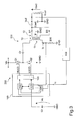
- FIG. 3 shows a resonant converter with a control device 100 in accordance with the present invention.
- the control device 100 controls a switching circuit 200 of the resonant converter; the switching circuit 200 comprises at least one half-bridge of at least first Q1 and second Q2 transistors connected between an input voltage Vin and a reference voltage, preferably the ground GND.
- the half-bridge 200 is adapted to generate a periodic square wave voltage ranging from a high voltage, corresponding to the input voltage Vin, to a low voltage, corresponding to the reference voltage GND; the half-bridge 200 drives a resonant circuit 300, preferably comprising a series of a capacitor Cr and a transformer 10 with a primary 11 and a center-tap secondary 12.
- the two windings of the center-tap secondary 12 of transformer 10 are connected to the anodes of two diodes D1 and D2 whose cathodes are both connected to the parallel of a capacitor Cout and a resistance Rout; the output voltage Vout of the resonant converter is present at the ends of said parallel while the output current Iout flows in said parallel.
- the control device 100 is adapted to control the half-bridge 200 according to the time period of discharging or charging a capacitor Ct outside the control device; the control device 100 is normally integrated in a silicon chip.
- the control device 100 alternately controls the switching on and off of the transistors Q1 and Q2; the control device 100 controls the switching on of transistor Q1 or transistor Q2 and the respective switching off of transistor Q2 or transistor Q1 according to the time period Tc of charging and/or discharging the external capacitor Ct.
- the control device 100 comprises circuit means 101 adapted to synchronize the starting time instant Tstart of the time period Tc of discharging or charging said capacitor Ct crossing the zero value of a signal Vs indicating the current Is flowing in the resonant circuit, in particular the voltage signal on the resistance Rs arranged between the primary 11 of transformer 10 and the ground GND.
- Device 100 further comprises means 102, 104 adapted to charge and discharge the capacitor Ct between a default minimum value Vv, GND and a default maximum value Vp.
- the control device 100 comprises further means 102, 103 adapted to control the switching off of said first Q1 or second Q2 transistor of the half-bridge at the end of the time period of charging or discharging the comparator Ct.
- Said further means 103 are particularly adapted to control the switching off of said first Q1 or second Q2 transistor of the half-bridge at the time instant T1 where the voltage at the ends of said capacitor reached said maximum value Vp or said minimum value Vv, GND.
- Said further means 103 are preferably adapted to control the switching off of transistor Q1 at the end of the time period of charging the external capacitor Ct, and the switching off of transistor Q2 at the end of the time period of discharging the external capacitor Ct.
- Means 103 drive the transistors Q1 and Q2 by the signals HSGD and LSGD.
- the signal Ic indicating the output voltage Vout or the output current lout is preferably carried on device 100 by an isolated coupler 400, for example an opto-coupler; said current signal Ic is preferably directly or indirectly used to charge or discharge the capacitor Ct from the circuit means 104.
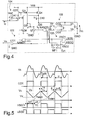
- FIG 4 shows a diagram of a control device for a resonant converter in accordance with a first embodiment of the present invention.
- the control current Ic (which is modulated by the control loop of the negative feedback output voltage) is taken out from the external pin connected to the inverting terminal of an operational amplifier OA1 having a reference voltage Vref on the non-inverting terminal; the output of the operational amplifier OA1 controls a bipolar transistor Q10 allowing the current Ic to be delivered towards a current mirror consisting of the bipolar transistors Q20-Q3, Q20-Q4.
- the bipolar transistor Q3 mirrors the current Ic towards another mirror consisting of the bipolar transistors Q5 and Q6, while the bipolar transistor Q4 delivers the current Ic towards the external capacitor Ct; the bipolar transistor Q6 allows the capacitor Ct to be discharged towards the ground GND.
- a diode D10 is connected between the transistors Q4 and Q6 to prevent the discharge current of the capacitor Ct from moving towards the transistor Q4.
- the operational amplifier OA1 with transistor Q10, the current mirror Q20-Q4 and the transistor Q8 belong to means 104.
- the voltage on the external capacitor Ct is zero.
- the comparator CO2 belonging to means 102 and adapted to compare the voltage Vc at the ends of the capacitor Ct with a reference voltage Vv, sets up the SR flip-flop FF1 so that the output Q becomes 1. After a delay of Td1, created by the monostable device MF1 having the output Q of the flip-flop FF1 at the input, together with port AND1, the output LSGD of the point AND1 becomes high and the transistor Q2 of the half-bridge 200 is switched on.
- a comparator CO1 belonging to means 101, is adapted to compare the voltage Vs with the ground GND, If the output of CO1 is firstly high, the output of port NAND1, receiving the negated output of the comparator CO1 and the output Q of the flip-flop FF1 at the input, is thus high; the transistor Q8, connected between transistor Q4 and the ground GND, is switched on and brings the current flowing in the bipolar transistor Q4 towards the ground.
- the current Ic from the transistor Q4 will charge the capacitor Ct and an ascendant voltage ramp of slope Ic/Ct will be observed thereon.
- Such a ramp is produced from the instant Tstart when the current of the resonant circuit is negative and, i.e., the sign thereof is the same as that of the voltage applied to the resonant circuit itself (negative per se when the transistor Q2 of the half-bridge is switched on).
- the comparator CO3 belonging to means 102 and adapted to compare the voltage Vc at the ends of the capacitor Ct with the reference voltage Vp, resets the SR flip-flop FF1 whose output Q becomes zero.
- This causes the half-bridge to be switched: the output LSGD immediately becomes zero and, after a delay Td1 generated by MF1 together with the port AND2, the output HSGD of the port AND2 becomes high, and the transistor Q1 of the half-bridge is switched on.
- the output of port NAND1 is forced high and the transistor Q8 is switched on; the current flowing through transistor Q4 is diverted towards the ground GND and the charge ramp of the capacitor Ct is cut off.
- the inversely polarized diode D10 isolates the capacitor Ct thus preventing it from discharging through the transistor Q8.
- the mirror Q5-Q6 was switched off.
- the signal Q is now high, whereby the output of said port depends on the status of the comparator CO1
- Due to the conduction period of the transistor Q2 of the half-bridge the current is negative when the half-bridge is negatively switched, whereby the output of comparator CO1 is still low, the output of port NAND2 is high, the transistor Q7 is switched on and the mirror Q5-Q6 is switched off; therefore the current admiting on capacitor Ct is zero and its voltage remains constant at about the value Vp.
- the discharge proceeds until the voltage Vc on capacitor Ct reaches the value Vv when the comparator CO2 sets the SR flip-flop FF1 again, bringing the output Q thereof high and still switching off the mirror Q5-Q6 and stopping the discharge of capacitor Ct.
- the output of port NAND1 is still high, since the current of the resonant circuit is still positive and the output of comparator CO1 is high, the transistor Q8 is switched on and the diode D10 is inversely polarized. Therefore the current insisting on the capacitor Ct is zero and its voltage remains constant at about Vv.
- Vv Vv + 1 Ct ⁇ Td Tsw / 2 Ic dt
- Tsw the switching time period of transistors Q1 and Q2.
- the feedback current Ic controls the time distance between the zero crossings of the current of the resonant circuit and the following switching of the half-bridge.
- control is not proportional to the phase (or its complement to ⁇ ), but to the reciprocal thereof, as a scale of the switching period of the half-bridge.
- Figure 5 shows the time charts of voltage Vs, Vc, voltage Vcol at the output of comparator CO1, and signals HSGD and LSGD.
- FIG. 6 shows a diagram of a control device for a resonant convener in accordance with a second embodiment of the present invention; the same elements as the diagram of the device in figure 4 will have the same reference numerals.
- the control current Ic (which is modulated by the control loop of the negative feedback output voltage) is taken out from the external pin connected to the inverting terminal of an operational amplifier OA1 having a reference voltage Vref on the non-inverting terminal; the output of the operational amplifier OA1 controls a bipolar transistor Q10 allowing the current Ic to be delivered towards a current mirror consisting of the bipolar transistors Q20-Q30 connected to the supply voltage Vdd.
- the mirror Q20-Q30 is switched on, i.e.
- the operational amplifier OA1 with transistor Q10, the current mirror Q20-Q30 and the transistor Q40 belong to means 104.
- the flip-flop FF1 will act as a Toggle at every positive edge applied to its asynchronous input from the comparator CO3, belonging to means 102, adapted to compare the voltage Vc at the ends of the capacitor Ct with the reference voltage Vp.
- the output of the comparator CO1 belonging to means 101 is firstly high, the output of the OR-exclusive port XOR1 receiving the output of comparator CO1 and the output Q of flip-flop FF1 at the input is thus high; the bipolar transistor Q40, which is connected between the supply voltage Vdd by means of the series of two resistances R1 and R2 and the ground GND, is switched on and the transistor Q50 having the base terminal connected to the common terminal of the two resistances R1 and R2 is also switched on, so that the mirror Q20-Q30 is switched off and the capacitor Ct is not charged.
- Such a ramp is produced from the instant when the current of the resonant circuit is negative and, i.e., the sign thereof is the same as that of the voltage applied to the resonant circuit itself (negative per se when the transistor Q2 of the half-bridge is switched on).
- the output of comparator CO3 becomes high thus inverting the status of the outputs of flip-flop FF1, whose output Q becomes one (and Q becomes zero).
- the signal Vs is still negative, whereby the output of comparator CO1 is low and the output of port XOR1 is forced high and therefore the transistor Q40 is switched on, thus quickly discharging the capacitor Ct to zero.
- the transistor Q40 also switches on the transistor Q50 which switches off the mirror Q20-Q30. This situation is kept as long as the voltage Vs remains negative.
- Such a ramp is produced from the instant when the current of the resonant circuit is positive and, i.e., the sign thereof is the same as that of the voltage applied to the resonant circuit itself (positive per se when the transistor Q1 of the half-bridge is switched on).
- the voltage now applied to the resonant circuit is negative whereby, after a short time, the current of the resonant circuit will also become negative, as well as the voltage Vs.
- the output of comparator CO1 becomes low and, therefore, also that of port NAND1; the transistor Q40 is switched off and the current flowing on transistor Q30 charges the capacitor Ct again, therefore starting a new switching cycle.
- the charge ramp is produced from the instant when the current of the resonant circuit is negative and, i.e., the sign thereof is the same as that of the voltage applied to the resonant circuit itself (negative per se when the transistor Q2 of the half-bridge is switched on).
- the ports AND1 and AND2 belong to means 103.
- the feedback current Ic controls the time distance between the zero crossings of the current of the resonant circuit and the following switching of the half-bridge.
- the equations describing the operation of this circuit are exactly the same as those given for the circuit in figure 4 .
- Figure 7 shows the time charts of voltage Vs, Vc, voltage Vcol on the output of the comparator CO1, and signals HSGD and LSGD.
- FIG 8 shows a resonant converter with a control device 100 in accordance with a third embodiment of the present invention wherein like reference numbers are used for like elements of the previous embodiments.
- the control device 100 controls a switching circuit 200 of the resonant converter; the switching circuit 200 comprises at least one half-bridge of at least first Q1 and second Q2 transistors connected between an input voltage Vin and a reference voltage, preferably the ground GND.
- the half-bridge 200 is adapted to generate a periodic square wave voltage ranging from a high voltage, corresponding to the input voltage Vin, to a low voltage, corresponding to the reference voltage GND; the half-bridge 200 drives a resonant circuit 300, preferably comprising a series of a capacitor Cr and a transformer 10 with a primary 11 and a center-tap secondary 12.
- the two windings of the center-tap secondary 12 of transformer 10 are connected to the anodes of two diodes D1 and D2 whose cathodes are both connected to the parallel of a capacitor Cout and a resistance Rout; the output voltage Vout of the resonant converter is present at the ends of said parallel while the output current Iout flows in said parallel.
- the control device 100 is adapted to control the half-bridge 200 according to the time period of charging a capacitor Ct outside the control device; the control device 100 is normally integrated in a silicon chip.
- the control device 100 alternately controls the switching on and off of the transistors Q1 and Q2; the control device 100 controls the switching on of transistor Q1 or transistor Q2 and the respective switching off of transistor Q2 or transistor Q1 according to the time period Tc of charging the external capacitor Ct.
- the control device 100 comprises circuit means 101 adapted to synchronize the starting time instant Tstart of the time period Tc of charging said capacitor Ct crossing the zero value of a signal Vs indicating the current Is flowing in the resonant circuit, in particular the voltage signal on the resistance Rs arranged between the primary 11 of transformer 10 and the ground GND.
- Device 100 further comprises means 105 adapted to generate a voltage Vpp having a value proportional to the duration of the switching period Tsw and means 102, 104 adapted to charge and discharge capacitor Ct between a reference voltage, preferably GND and voltage Vpp.
- the control device 100 comprises means 102, 103 adapted to control the switching off of said first Q1 or second Q2 transistor of the half-bridge at the end of the time period of charging or discharging the comparator Ct.
- Means 103 are particularly adapted to control the switching off of said first Q1 or second Q2 transistor of the half-bridge at the time instant T1 where the voltage at the ends of said capacitor reached said voltage Vpp.
- Means 103 are preferably adapted to control the switching off of transistor Q1 at the end of time period Tc of charging the external capacitor Ct, and the switching off of transistor Q2 at the next time period Tc of charging the external capacitor Ct in a switching cycle Tsw.
- Means 103 drive the transistors Q1 and Q2 by the signals HSGD and LSGD.
- the signal Ic indicating the output voltage Vout or the output current Iout is preferably carried on device 100 by an isolated coupler 400, for example an opto-coupler; said current signal Ic is preferably directly or indirectly used to charge or discharge capacitor Ct from circuit means 104.
- FIG. 9 shows a more detailed diagram of a control device for a resonant converter in accordance with the third embodiment of the present invention.
- the control current Ic (which is modulated by the control loop of the negative feedback output voltage) is taken out from the external pin connected to the inverting terminal of an operational amplifier OA1 having a reference voltage Vref on the non-inverting terminal; the output of operational amplifier OA1 controls a bipolar transistor Q10 allowing the current Ic to be delivered towards a current mirror consisting of the bipolar transistors Q20-Q30 connected to the supply voltage Vdd.
- mirror Q20-Q30 is on, i.e.
- the operational amplifier OA1 with transistor Q10, the current mirror Q20-Q30 and the transistor Q40 belong to means 104.
- flip-flop FF1 will operate as a Toggle at every positive edge applied to the asynchronous input thereof by the comparator CO3, belonging to means 102, adapted to compare the voltage Vc at the ends of capacitor C with voltage Vpp.
- the output of comparator CO1, belonging to means 101 is firstly high, the output of the exclusive-OR port X-OR1, receiving at the input the output of comparator CO and the output Q of flip-flop FF1 is thus high; the bipolar transistor Q40, which is connected between supply voltage Vdd by the series of two resistances R1 and R2 and ground GND, is switched on as well as the transistor Q50, having the base terminal connected to the common terminal of the two resistances R1 and R2, so that mirror Q20-Q30 is switched off and capacitor Ct is not charged.
- Such a ramp is produced from the instant when the current of the resonant circuit is negative and, i.e., the sign thereof is the same as that of the voltage applied to the resonant circuit itself (negative per se when the transistor Q2 of the half-bridge is switched on).
- the feedback current Ic controls the time distance between the zero crossings of the current of the resonant circuit and the following switching of the half-bridge.
- Voltage Vpp is produced by means 105 adapted to proportionally generate the signal Vpp to the switching period Tsw,
- the base terminal of transistor Q60 is controlled by signal Q output from the flip-flop FF1, which occurs when the output Q of flip-flop FF1 is low, i.e, over all the time between the moment when signal LSGD becomes low and the moment when signal HSGD becomes low
- Said current h Im is diverted, instead, towards ground when transistor Q60 is switched on, which occurs when the output Q of flip-flop FF1 is high, i.e. over all the time between the moment when signal HSGD becomes low and the moment when signal LSGD becomes low, essentially corresponding to the second half of the switching period Tsw.
- Means 105 comprise a sampler 500 whose control input, sensitive to the positive edges, is driven by signal Q and adapted to sample the voltage on capacitor Ch.
- the voltage Vpp is thus a continuous level proportional to the switching period Tsw.
- the transistor Q6 discharging capacitor Ch is switched on with a short delay Td given by a block Delay with respect to the sampling moment, in order to avoid errors.
- control is not proportional to the phase (or its complement to ⁇ ), but to 1 / (1 - ⁇ / ⁇ ).
- the mirror factors h and k should not preferably be chosen as being too different from each other, possibly equal: thereby, exploiting "matching" techniques, though having their individual values of considerable static dispersions, their ratio has instead a very small static dispersion.
- capacities Ct and Ch which may conveniently be chosen as equal to each other.
- control device for resonant converters of the third embodiment of the present invention the operational limits of the converter can be set independent from the dispersion of the parameters of the resonant circuit, so as to improve the strength of the control.
Abstract
Description
- The present invention relates to a control device for resonant converters.
- Forced switching converters (switching converters) with devices used for controlling them are known in the state of the art. The resonant converters are a wide range of forced switching converters characterized by the presence of a resonant circuit playing an active part in determining the input-output power flow. In these converters, a bridge (half-bridge) consisting of four (two) power switches (typically MOSFET powers) which is fed by a direct voltage generates a voltage square wave which is applied to a resonant circuit tuned in to a frequency close to the fundamental frequency of said square wave. Thereby, because of its selective features, the resonant circuit mainly responds to this fundamental component, while negligibly to the superior harmonics. As a result, the circulating power may be modulated by changing the frequency of the square wave, keeping the duty cycle constant at 50% and, according to the resonant circuit configuration, the currents and/or voltages associated with the power flow have a sinusoidal or a gated sinusoidal development.
- These voltages are adjusted and filtered so as to provide d.c. power on the load. In network applications, for security requirement issues, the adjusting and filtering system feeding the load is coupled with the resonant circuit by a transformer providing the isolation between source and load required by the above-mentioned regulations. As for all the isolated network converters, also in this case a primary side (as it regards the primary winding of the transformer) connected to the input source is distinguished from a secondary side (as it regards the secondary winding - or the secondary windings - of the transformer) providing power to the load through the adjusting and filtering system.
- Among the many types of resonant converters, the so-called LLC resonant converter, especially in the half-bridge version thereof, is currently often used. Such a designation comes from that the resonant circuit employs two inductors (L) and a capacitor (C); a diagram of LLC resonant converter is shown in
figure 1 .Resonant converter 1 comprises a half-bridge of transistors Q1 and Q2 between the input voltage Vin and the ground GND and driven by adriving circuit 3. The common terminal HB between the transistors Q1 and Q2 is connected to acircuit block 2 comprising a series of a capacitor Cr, an inductance Ls and another inductance Lp connected to the parallel of atransformer 10 with a center-tap secondary. The two windings of the center-tap secondary oftransformer 10 are connected to the anodes of two diodes D1 and D2 whose cathodes are both connected to the parallel of a capacitor Cout and a resistance Rout; at the ends of said parallel, there is the output voltage Vout of the resonant converter, while the output current lout flows in said parallel. - The resonant converters offer considerable advantages as compared to the traditional switching converters (non-resonant, typically PWM - Pulse Width Modulation - controlled): wave forms without steep edges, low switching losses of the power switches due to their "soft" switching, high conversion efficiency (>95% is easily reachable), operation ability at high frequencies, low EMI (Electro Magnetic Interference) generation and, ultimately, high power density (that is, the ability of achieving conversion systems capable of handling considerable powers in reduced volumes).
- As in most dc-dc converters, a closed loop, negative feedback adjustment system keeps the output voltage of the converter constant as the operational conditions vary, that is the input voltage Vin and/or the output current lout thereof. This is achieved by comparing a portion of the output voltage with a reference voltage Vref; the difference or error signal Er between the value provided by the output voltage reading system (usually, a resistance divider) and the reference value is amplified by an error amplifier whose output Vc modifies a value x inside the converter on which the energy carried by the converter in each switching cycle substantially depends. As set forth above, such a very significant value in resonant converters is the switching frequency of the square wave stimulating the resonant circuit.
- Again, as it is common in all the adjustment systems of the dc-dc converters, the frequency response of the error amplifier must be conveniently designed so as to ensure:
- the stability of the control loop (i.e., the fact that upon perturbations of the operational conditions of the converter, once the transient caused by the perturbation is over, the output voltage tends to recover a constant value close to the value before the perturbation;
- a good adjustment (i.e., the new constant value recovered by the output voltage following a perturbation is very close to that before the perturbation);
- good dynamic features (i.e., during the transient upon a perturbation the output voltage is not so different from the desired value and the transient itself is short).
- The above-mentioned control objectives may be expressed in terms of some characteristic values of the transfer function of the adjustment loop, such as the bandwidth, the phase margin, the d.c. gain. In an assigned dc-dc converter, these objectives may be achieved by acting on the frequency response of the error amplifier, by modifying the gain thereof and conveniently deploying the poles and zeroes of its transfer function (frequency compensation), which is normally achieved by using reactive networks comprising resistances and capacities of convenient value connected thereto.
- In order to determine which is the required frequency compensation to obtain the desired features of the transfer function of the adjustment loop, however, it should be known both the gain of the modulator, i.e. the system converting the control voltage Vc into the control value x, as well as the frequency response of the converter itself to the variations of value x.
- The modulator gain does not usually depend on the frequency, at least within the range of the relevant frequencies, which may not be higher than half of the switching Frequency of the converter by virtue of Shannon's theorem and it is fixed within the control integrated circuit.
- As far as the frequency response of a de-de converter, even in the presence of a strongly non-linear system just because of the switching action, with convenient approximations and under certain hypothesis, this may be described and represented by the same means used for the linear networks and, therefore, by a transfer function characterized by gain, zeroes and poles. This transfer function essentially depends on the topology of the converter, i.e, on the mutual configuration of the elements handling the power, the operation mode thereof, i.e. whether, at every switching cycle, there is a continuous current circulation in the magnetic part (Continuous Current Mode, CCM) or not (Discontinuous Current Mode, DCM), the value x which is controlled by the adjustment loop. While in PWM converters different control methods are commonly used - e.g. the width of the pulse controlling the power switches (direct duty cycle control and, therefore, x=D) or the peak of the current flowing through the switches (peak current mode control, x = Ip) are directly acted upon - traditionally, in resonant converters, the value used to control the converter is directly the switching frequency of the square wave applied to the resonant circuit.
- In all the integrated control circuits for dc-dc resonant converters present on the market, the control directly operates on the oscillation frequency of the half-bridge (Direct Frequency Converter, DFC).
Figure 2 shows a control system for this type of resonant converters. The output of theerror amplifier 4, having a part of the output voltage Vout at the input of the inverting terminal and a reference voltage Vref on the non-inverting terminal, on the secondary side is transferred to the primary side by aphotocoupler 5 so as to ensure the primary-secondary isolation according to the security requirements and acts upon a voltage-controlled oscillator (VCO) 6 or a current-controlled oscillator (ICO) inside the control integratedcircuit 30. This type of control arises two classes of problems. A first class relates to that in literature the small-signal dynamic patterns for resonant converters expressed in terms of gain, poles and zeroes are not known (but in some approximated forms of practical arguable use), differently from what occurs, instead, for PWM converters, i.e. the transfer function of the power stage is not known. A second class of problems relates to that, according to study results based on simulations, said transfer function of the power stage shows a strongly variable d.c. gain, and a variable number of poles from one to three and with very moving deployment, depending on the operational point. Finally, there is a zero due to the output capacitor. The considerable variation of the gain and the so-highly variable pole configuration make the compensation of the frequency of the feedback control loop quite problematic. As a result, it is virtually impossible to obtain a transient response optimized under all the operational conditions, and the compromise level between stability and dynamic performances is high. Furthermore, there is a strong dependence of the energy transfer on the input voltage (audio susceptibility), whereby the control loop must strongly intervene and considerably change the operational frequency for compensating said variations. Taking into account that an alternate component with a double frequency as compared to that of the network voltage always exists in the input voltage of the converter, the loop gain at that frequency needs to be quite high, so as to effectively reject said alternate component and considerably attenuate the residual ripple visible in the output voltage. All these factors risk to arise problems not completely solvable, particularly when the load fed by the converter has considerable dynamics and/or the specifications of dynamic accuracy and response readiness are strict, or yet still when there are restraining requirements on the rejection of the ripple of the input voltage. Finally, another problem related to the DFC control method is that of the static dispersion of values of the components of the resonant circuit (Cr, Ls and Lp) due to their tolerances. Indeed, generally speaking, in order to avoid a converter from abnormally operating, the control value x should be limited. In this case, the resonant controllers implementing DFC allow the operational frequency of the half-bridge to be high- and low-limited. These limits should be set up by taking into account that, due to the above-mentioned value dispersion, the operational frequency range of the converter will change accordingly. Therefore, the minimum limit imposed to the frequency should be lower than the minimum value which could be taken by the lower end of said range, and the maximum limit should be higher than the maximum value which could be taken by the higher end of said range. This considerably reduces the effectiveness of the frequency limitation as a mean for preventing abnormal operational conditions. - One art reported in literature is that described in the article "Self-Sustained Oscillating Resonant Converters Operating Above the Resonant Frequency" to H. Pinheiro, P. K. Jain, and G. Joós, published in IEEE Transactions on Power Electronics, Vol. 14, No. 5, September 1999, p. 803-814, wherein the value x which is controlled by the feedback loop is the phase shifting between the current of the resonant circuit and the square wave voltage applied to said circuit by the half-bridge or bridge. In the above-mentioned article it is shown that the features of a system controlled according to this method are similar to those of the systems controlled under charge control, from the point of view of both the small and wide signal dynamics. On the other hand, over said systems controlled under charge control there is a considerable advantage: the obtained system is absolutely stable in any operational conditions, as long as the current of the resonant circuit is late with respect to the voltage applied thereto. This restraint coincides with the necessary condition to obtain the "soft" switching for the MOSFET transistors belonging to the half-bridge.
- In view of the state of the art, it is an object of the present invention to provide a control device for resonant converters which is easier than those known.
- In accordance with the present invention, said object is achieved by a control device of a switching circuit for a resonant converter having a direct current at the output, said switching circuit comprising at least a half-bridge of at least first and second transistors connected between an input voltage and a reference voltage, said half-bridge being adapted to generate a periodic square wave voltage to drive the resonant circuit of said resonant converter, said periodic square wave voltage ranging from a high voltage corresponding to the input voltage to a low voltage corresponding to the reference voltage, said control device being adapted to control said half-bridge according to the time period of charging or discharging a capacitor, characterized in that it comprises circuit means adapted to synchronize the starting time instant of the time period of discharging or charging said capacitor crossing the zero value of a signal indicating the current flowing in the resonant circuit, and further means adapted to control the switching off of said first or said second transistor at the end of the time period of discharging or charging the capacitor.
- By virtue of the present invention, a control device for resonant converters may be provided, which allows the dynamic order of the converter to be reduced; by possibly making it equivalent to a single-pole system (at least in the relevant frequency range from the point of view of the frequency compensation design), so as to improve the transient response thereof to the load variations.
- Said control device further reduces the audio susceptibility of the converter, either through a reduced sensitivity to the variations of the input voltage and/or to the possibility of being able to set up the loop gain in a more free manner, so as to improve both the transient response to the variations of the input voltage, and the rejection of the input voltage ripple.
- Said control device also allows the operational limits of the converter to be set up regardless the dispersion of the resonant circuit parameters, so as to improve the strength of the control.
- The features and advantages of the present invention will be apparent from the following detailed description of practical embodiments thereof, shown by way of non-limiting example in the accompanying drawings, in which:
-
figure 1 shows a diagram of a LLC resonant converter in accordance with the known art; -
figure 2 shows a block diagram of a resonant converter with adjustment of the output voltage in accordance with the known art; -
figure 3 shows a diagram of a resonant converter with control device in accordance with the present invention; -
figure 4 shows a diagram of a control device for resonant converter in accordance with a first embodiment of the present invention; -
figure 5 shows time charts of the voltages involved in the device infigure 4 ; -
figure 6 shows a diagram of a control device for resonant converter in accordance with a second embodiment of the present invention; -
figure 7 shows time charts of the voltages involved in the device infigure 6 ; -
figure 8 shows a diagram of a resonant converter with a control device in accordance with a third embodiment of the present invention; -
figure 9 shows a more detailed diagram of the control device for a resonant converter in accordance with the third embodiment of the present invention; -
figure 10 shows some time charts of the relevant voltages in the device offigure 9 . -
Figure 3 shows a resonant converter with acontrol device 100 in accordance with the present invention. Thecontrol device 100 controls aswitching circuit 200 of the resonant converter; theswitching circuit 200 comprises at least one half-bridge of at least first Q1 and second Q2 transistors connected between an input voltage Vin and a reference voltage, preferably the ground GND. The half-bridge 200 is adapted to generate a periodic square wave voltage ranging from a high voltage, corresponding to the input voltage Vin, to a low voltage, corresponding to the reference voltage GND; the half-bridge 200 drives aresonant circuit 300, preferably comprising a series of a capacitor Cr and atransformer 10 with a primary 11 and a center-tap secondary 12. The two windings of the center-tap secondary 12 oftransformer 10 are connected to the anodes of two diodes D1 and D2 whose cathodes are both connected to the parallel of a capacitor Cout and a resistance Rout; the output voltage Vout of the resonant converter is present at the ends of said parallel while the output current Iout flows in said parallel. - The
control device 100 is adapted to control the half-bridge 200 according to the time period of discharging or charging a capacitor Ct outside the control device; thecontrol device 100 is normally integrated in a silicon chip. Thecontrol device 100 alternately controls the switching on and off of the transistors Q1 and Q2; thecontrol device 100 controls the switching on of transistor Q1 or transistor Q2 and the respective switching off of transistor Q2 or transistor Q1 according to the time period Tc of charging and/or discharging the external capacitor Ct. - The
control device 100 comprises circuit means 101 adapted to synchronize the starting time instant Tstart of the time period Tc of discharging or charging said capacitor Ct crossing the zero value of a signal Vs indicating the current Is flowing in the resonant circuit, in particular the voltage signal on the resistance Rs arranged between the primary 11 oftransformer 10 and the ground GND.Device 100 further comprisesmeans - The
control device 100 comprises further means 102, 103 adapted to control the switching off of said first Q1 or second Q2 transistor of the half-bridge at the end of the time period of charging or discharging the comparator Ct. Said further means 103 are particularly adapted to control the switching off of said first Q1 or second Q2 transistor of the half-bridge at the time instant T1 where the voltage at the ends of said capacitor reached said maximum value Vp or said minimum value Vv, GND. Said further means 103 are preferably adapted to control the switching off of transistor Q1 at the end of the time period of charging the external capacitor Ct, and the switching off of transistor Q2 at the end of the time period of discharging the external capacitor Ct.Means 103 drive the transistors Q1 and Q2 by the signals HSGD and LSGD. - The signal Ic indicating the output voltage Vout or the output current lout is preferably carried on
device 100 by anisolated coupler 400, for example an opto-coupler; said current signal Ic is preferably directly or indirectly used to charge or discharge the capacitor Ct from the circuit means 104. -
Figure 4 shows a diagram of a control device for a resonant converter in accordance with a first embodiment of the present invention. For simplicity all the mirrors are assumed to have a mirroring rate of 1. The control current Ic (which is modulated by the control loop of the negative feedback output voltage) is taken out from the external pin connected to the inverting terminal of an operational amplifier OA1 having a reference voltage Vref on the non-inverting terminal; the output of the operational amplifier OA1 controls a bipolar transistor Q10 allowing the current Ic to be delivered towards a current mirror consisting of the bipolar transistors Q20-Q3, Q20-Q4. The bipolar transistor Q3 mirrors the current Ic towards another mirror consisting of the bipolar transistors Q5 and Q6, while the bipolar transistor Q4 delivers the current Ic towards the external capacitor Ct; the bipolar transistor Q6 allows the capacitor Ct to be discharged towards the ground GND. A diode D10 is connected between the transistors Q4 and Q6 to prevent the discharge current of the capacitor Ct from moving towards the transistor Q4. The operational amplifier OA1 with transistor Q10, the current mirror Q20-Q4 and the transistor Q8 belong tomeans 104. - First, the voltage on the external capacitor Ct is zero. The comparator CO2, belonging to
means 102 and adapted to compare the voltage Vc at the ends of the capacitor Ct with a reference voltage Vv, sets up the SR flip-flop FF1 so that the output Q becomes 1. After a delay of Td1, created by the monostable device MF1 having the output Q of the flip-flop FF1 at the input, together with port AND1, the output LSGD of the point AND1 becomes high and the transistor Q2 of the half-bridge 200 is switched on. - A comparator CO1, belonging to
means 101, is adapted to compare the voltage Vs with the ground GND, If the output of CO1 is firstly high, the output of port NAND1, receiving the negated output of the comparator CO1 and the output Q of the flip-flop FF1 at the input, is thus high; the transistor Q8, connected between transistor Q4 and the ground GND, is switched on and brings the current flowing in the bipolar transistor Q4 towards the ground. - When the signal Vs becomes negative (there will be parasitic current oscillations of the resonant circuit due to Q1 being switched on), the output of comparator CO1 will become low, the inputs of port NAND1 will be both high and, therefore, the output thereof will become low. Transistor Q8 is switched off and the current mirrored from the transistor Q4 is diverted on the capacitor Ct through the diode D10. On the other hand, the output
Q of the flip-flop FF1 being low, the output of port NAD2 receiving said signal Q and the output of the comparator CO1 are high, whereby transistor Q7 connected between the common base terminals of transistors Q5 and Q6 and the ground GND, is switched on and keeps the mirror Q5-Q6 switched off. The current Ic from the transistor Q4 will charge the capacitor Ct and an ascendant voltage ramp of slope Ic/Ct will be observed thereon. Such a ramp is produced from the instant Tstart when the current of the resonant circuit is negative and, i.e., the sign thereof is the same as that of the voltage applied to the resonant circuit itself (negative per se when the transistor Q2 of the half-bridge is switched on). - As soon as the voltage on the capacitor Ct reaches the reference voltage Vp at the time instant T1, the comparator CO3 belonging to
means 102 and adapted to compare the voltage Vc at the ends of the capacitor Ct with the reference voltage Vp, resets the SR flip-flop FF1 whose output Q becomes zero. This causes the half-bridge to be switched: the output LSGD immediately becomes zero and, after a delay Td1 generated by MF1 together with the port AND2, the output HSGD of the port AND2 becomes high, and the transistor Q1 of the half-bridge is switched on. The output of port NAND1 is forced high and the transistor Q8 is switched on; the current flowing through transistor Q4 is diverted towards the ground GND and the charge ramp of the capacitor Ct is cut off. The inversely polarized diode D10 isolates the capacitor Ct thus preventing it from discharging through the transistor Q8. Up to now, the mirror Q5-Q6 was switched off. At the input of port NAND2, however, the signalQ is now high, whereby the output of said port depends on the status of the comparator CO1, Due to the conduction period of the transistor Q2 of the half-bridge, the current is negative when the half-bridge is negatively switched, whereby the output of comparator CO1 is still low, the output of port NAND2 is high, the transistor Q7 is switched on and the mirror Q5-Q6 is switched off; therefore the current insisting on capacitor Ct is zero and its voltage remains constant at about the value Vp. Due to switching, however, the voltage now applied to the resonant circuit is positive, whereby after a short time also the current of the resonant circuit and the voltage Vs will become positive. The output of CO1 becomes high, that of NAND2 with both inputs high becomes low and the mirror Q5-Q6 switches on taking out a current equal to Ic from the capacitor Ct by discharging it. A descendant voltage ramp of slope -Ic/Ct will be observed thereon. Such a ramp is produced from the instant when the current of the resonant circuit is positive and the sign thereof is the same as that of the voltage applied to the resonant circuit itself (positive per se when the MOSFET Q1 of the half-bridge is switched on). - The discharge proceeds until the voltage Vc on capacitor Ct reaches the value Vv when the comparator CO2 sets the SR flip-flop FF1 again, bringing the output Q thereof high and still switching off the mirror Q5-Q6 and stopping the discharge of capacitor Ct. The output of port NAND1 is still high, since the current of the resonant circuit is still positive and the output of comparator CO1 is high, the transistor Q8 is switched on and the diode D10 is inversely polarized. Therefore the current insisting on the capacitor Ct is zero and its voltage remains constant at about Vv.
- Due to switching, however, the voltage now applied to the resonant circuit is negative whereby, after a short time, the current of the resonant circuit and the voltage Vs will also become negative. The output of comparator CO1 becomes low and, therefore, also that of NAND1, the transistor Q8 is switched off and the current flowing on transistor Q4 charges the capacitor Ct again, thus starting a new switching cycle. The charging ramp is produced from the instant when the current of the resonant circuit is negative and, i.e., the sign thereof is the same as that of the voltage applied to the resonant circuit itself (negative per se when the MOSFET Q2 of the half-bridge is switched on). The ports AND1 and AND2 belong to
means 103. - The equation describing the charge of capacitor Ct, in a switching half-period, by denoting with Vv (for example equal to 1V) the downstream voltage of the waveform on the capacitor Ct and Vp (for example equal to 4V) the peak voltage of said waveform, may be written as:

- It is inferred therefrom:

- Therefore, the feedback current Ic controls the time distance between the zero crossings of the current of the resonant circuit and the following switching of the half-bridge. By denoting with Φ the phase angle between the resonant current and the voltage of the half-bridge, it is apparent that the control affects the angle π - Φ, thus determining the time Tc=Tsw/2 - Td. On the other hand, as it is apparent, the following may be written:


Figure 5 shows the time charts of voltage Vs, Vc, voltage Vcol at the output of comparator CO1, and signals HSGD and LSGD. -
Figure 6 shows a diagram of a control device for a resonant convener in accordance with a second embodiment of the present invention; the same elements as the diagram of the device infigure 4 will have the same reference numerals. The control current Ic (which is modulated by the control loop of the negative feedback output voltage) is taken out from the external pin connected to the inverting terminal of an operational amplifier OA1 having a reference voltage Vref on the non-inverting terminal; the output of the operational amplifier OA1 controls a bipolar transistor Q10 allowing the current Ic to be delivered towards a current mirror consisting of the bipolar transistors Q20-Q30 connected to the supply voltage Vdd. When the mirror Q20-Q30 is switched on, i.e. when the bipolar transistor Q50 having the collector and emitter terminals coupled between the supply voltage Vdd and the base terminal of transistors Q20 and Q30, it mirrors the current Ic towards the external capacitor Ct thus allowing the latter to be charged; when it is switched on, transistor Q40 allows the capacitor Ct to be quickly discharged towards the ground GND while switching off the mirror Q20-Q30 to reduce the overall current consumption. This last task is not essential for the operation of the circuit. The operational amplifier OA1 with transistor Q10, the current mirror Q20-Q30 and the transistor Q40 belong tomeans 104. - Firstly, the voltage Vc on the external capacitor Ct is zero. The
initialization circuit 50 sets up the inputs J and K of the flip-flop FF1 to 0 and 1, respectively, so that the output Q thereof is low (and, therefore, the complementaryQ thereof is high), then it sets J = K = 1. Thereby, from now, the flip-flop FF1 will act as a Toggle at every positive edge applied to its asynchronous input from the comparator CO3, belonging tomeans 102, adapted to compare the voltage Vc at the ends of the capacitor Ct with the reference voltage Vp.Q being asserted high, after a delay of Td1 created by the monostable device MF1 having the output Q of the flip-flop FF1 at the input, together with port AND1, the output LSGD becomes high and the transistor Q2 of the half-bridge 200 is switched on. If the output of the comparator CO1 belonging to means 101 is firstly high, the output of the OR-exclusive port XOR1 receiving the output of comparator CO1 and the output Q of flip-flop FF1 at the input is thus high; the bipolar transistor Q40, which is connected between the supply voltage Vdd by means of the series of two resistances R1 and R2 and the ground GND, is switched on and the transistor Q50 having the base terminal connected to the common terminal of the two resistances R1 and R2 is also switched on, so that the mirror Q20-Q30 is switched off and the capacitor Ct is not charged. - When the signal Vs becomes negative (there will be parasitic current oscillations of the resonant circuit due to Q1 being switched on), the output of the comparator CO1 will become low, the inputs of the port XOR1 will be both high and, therefore, the output thereof will become low. Transistor Q40 is switched off, transistor Q50 is switched off accordingly and mirror Q20-Q30 is switched on, so that the current flowing through transistor Q30 charges the capacitor Ct and an ascendant voltage ramp of slope Ic/Ct will be observed thereon. Such a ramp is produced from the instant when the current of the resonant circuit is negative and, i.e., the sign thereof is the same as that of the voltage applied to the resonant circuit itself (negative per se when the transistor Q2 of the half-bridge is switched on).
- As soon as the voltage Vc on the capacitor Ct reaches the reference voltage Vp, the output of comparator CO3 becomes high thus inverting the status of the outputs of flip-flop FF1, whose output Q becomes one (and
Q becomes zero). This causes the half-bridge to be switched: the output LSGD immediately becomes zero and, after a delay Td1 generated by the monostable device MF1 together with the port AND2, the output HSGD becomes high, and the transistor Q1 of the half-bridge 200 is switched on. The signal Vs is still negative, whereby the output of comparator CO1 is low and the output of port XOR1 is forced high and therefore the transistor Q40 is switched on, thus quickly discharging the capacitor Ct to zero. At the same time, the transistor Q40 also switches on the transistor Q50 which switches off the mirror Q20-Q30. This situation is kept as long as the voltage Vs remains negative. - Due to switching, however, the voltage now applied to the resonant circuit is positive whereby, after a short time, the current of the resonant circuit will also become positive, as well as the voltage Vs. The output of comparator CO1 becomes high, that of point XOR1, with both inputs being high, becomes low, the transistors Q40 and Q50 switch off and the mirror Q20-Q30 switches on thus charging the capacitor Ct with the current Ic. An ascendant voltage ramp of slope Ic/Ct will be observed thereon. Such a ramp is produced from the instant when the current of the resonant circuit is positive and, i.e., the sign thereof is the same as that of the voltage applied to the resonant circuit itself (positive per se when the transistor Q1 of the half-bridge is switched on).
- The discharge proceeds until the voltage on the capacitor Ct reaches the value Vp once again, and the output of CO3 becomes high, therefore inverting the status of the outputs of FF1, whose output Q becomes zero (and
Q becomes one). This causes the half-bridge to be switched: the output HSGD immediately becomes zero and, after a delay Td generated by MF1 together with the port AND1, the output LSGD becomes high, and the transistor Q2 of the half-bridge is switched on. The voltage signal Vs is still positive, whereby the output of CO1 is high and the output of the port XOR1 is forced high and therefore the transistor Q40 is switched on, thus quickly discharging the capacitor Ct to zero. At the same time, the transistor Q40 also switches on the transistor Q50 which switches off the mirror Q20-Q30. This situation is kept as long as the voltage Vs remains positive. - Due to switching, however, the voltage now applied to the resonant circuit is negative whereby, after a short time, the current of the resonant circuit will also become negative, as well as the voltage Vs. The output of comparator CO1 becomes low and, therefore, also that of port NAND1; the transistor Q40 is switched off and the current flowing on transistor Q30 charges the capacitor Ct again, therefore starting a new switching cycle. Once again, the charge ramp is produced from the instant when the current of the resonant circuit is negative and, i.e., the sign thereof is the same as that of the voltage applied to the resonant circuit itself (negative per se when the transistor Q2 of the half-bridge is switched on). The ports AND1 and AND2 belong to
means 103. - Even in this case, the feedback current Ic controls the time distance between the zero crossings of the current of the resonant circuit and the following switching of the half-bridge. The equations describing the operation of this circuit are exactly the same as those given for the circuit in
figure 4 . -
Figure 7 shows the time charts of voltage Vs, Vc, voltage Vcol on the output of the comparator CO1, and signals HSGD and LSGD. -
Figure 8 shows a resonant converter with acontrol device 100 in accordance with a third embodiment of the present invention wherein like reference numbers are used for like elements of the previous embodiments. Thecontrol device 100 controls aswitching circuit 200 of the resonant converter; theswitching circuit 200 comprises at least one half-bridge of at least first Q1 and second Q2 transistors connected between an input voltage Vin and a reference voltage, preferably the ground GND. The half-bridge 200 is adapted to generate a periodic square wave voltage ranging from a high voltage, corresponding to the input voltage Vin, to a low voltage, corresponding to the reference voltage GND; the half-bridge 200 drives aresonant circuit 300, preferably comprising a series of a capacitor Cr and atransformer 10 with a primary 11 and a center-tap secondary 12. The two windings of the center-tap secondary 12 oftransformer 10 are connected to the anodes of two diodes D1 and D2 whose cathodes are both connected to the parallel of a capacitor Cout and a resistance Rout; the output voltage Vout of the resonant converter is present at the ends of said parallel while the output current Iout flows in said parallel. - The
control device 100 is adapted to control the half-bridge 200 according to the time period of charging a capacitor Ct outside the control device; thecontrol device 100 is normally integrated in a silicon chip. Thecontrol device 100 alternately controls the switching on and off of the transistors Q1 and Q2; thecontrol device 100 controls the switching on of transistor Q1 or transistor Q2 and the respective switching off of transistor Q2 or transistor Q1 according to the time period Tc of charging the external capacitor Ct. - The
control device 100 comprises circuit means 101 adapted to synchronize the starting time instant Tstart of the time period Tc of charging said capacitor Ct crossing the zero value of a signal Vs indicating the current Is flowing in the resonant circuit, in particular the voltage signal on the resistance Rs arranged between the primary 11 oftransformer 10 and the ground GND.Device 100 further comprisesmeans 105 adapted to generate a voltage Vpp having a value proportional to the duration of the switching period Tsw and means 102, 104 adapted to charge and discharge capacitor Ct between a reference voltage, preferably GND and voltage Vpp. - The
control device 100 comprisesmeans Means 103 are particularly adapted to control the switching off of said first Q1 or second Q2 transistor of the half-bridge at the time instant T1 where the voltage at the ends of said capacitor reached said voltage Vpp.Means 103 are preferably adapted to control the switching off of transistor Q1 at the end of time period Tc of charging the external capacitor Ct, and the switching off of transistor Q2 at the next time period Tc of charging the external capacitor Ct in a switching cycle Tsw.Means 103 drive the transistors Q1 and Q2 by the signals HSGD and LSGD. - The signal Ic indicating the output voltage Vout or the output current Iout is preferably carried on
device 100 by anisolated coupler 400, for example an opto-coupler; said current signal Ic is preferably directly or indirectly used to charge or discharge capacitor Ct from circuit means 104. -
Figure 9 shows a more detailed diagram of a control device for a resonant converter in accordance with the third embodiment of the present invention. For simplicity, all current mirrors are assumed to have a mirroring ratio of 1. The control current Ic (which is modulated by the control loop of the negative feedback output voltage) is taken out from the external pin connected to the inverting terminal of an operational amplifier OA1 having a reference voltage Vref on the non-inverting terminal; the output of operational amplifier OA1 controls a bipolar transistor Q10 allowing the current Ic to be delivered towards a current mirror consisting of the bipolar transistors Q20-Q30 connected to the supply voltage Vdd. When mirror Q20-Q30 is on, i.e. when the bipolar transistor Q50 having the collector and emitter terminals coupled between the supply voltage Vdd and the base terminal of transistors Q20 and Q30 is off, it mirrors the current Ic towards external capacitor Ct, thus allowing the latter to be charged; when transistor Q40 is on, it allows capacitor Ct to be quickly discharged to ground GND while switching off mirror Q20-Q30 for reducing the overall current consumption. The latter task is not essential for the operation of the circuit. The operational amplifier OA1 with transistor Q10, the current mirror Q20-Q30 and the transistor Q40 belong tomeans 104. - First, the voltage Vc on external capacitor Ct is zero. The
initialization circuit 50 sets inputs J and K of a flip-flop FF1 to 0 and 1, respectively, so as the output Q thereof is low (and, therefore, the complementaryQ thereof is high), then J = K = 1 is set. Thereby, from now on, flip-flop FF1 will operate as a Toggle at every positive edge applied to the asynchronous input thereof by the comparator CO3, belonging tomeans 102, adapted to compare the voltage Vc at the ends of capacitor C with voltage Vpp.Q being claimed high, after a delay equal to Td1, created by the monostable device MF1 having at the input the output Q of flip-flop FF1, along with the port AND1, the output LSGD becomes high and transistor Q2 of half-bridge 200 is switched on. If the output of comparator CO1, belonging tomeans 101, is firstly high, the output of the exclusive-OR port X-OR1, receiving at the input the output of comparator CO and the output Q of flip-flop FF1 is thus high; the bipolar transistor Q40, which is connected between supply voltage Vdd by the series of two resistances R1 and R2 and ground GND, is switched on as well as the transistor Q50, having the base terminal connected to the common terminal of the two resistances R1 and R2, so that mirror Q20-Q30 is switched off and capacitor Ct is not charged. - When signal Vs becomes negative (there will be parasitic current oscillations of the resonant circuit due to Q1 being switched on), the output of comparator CO1 will become low, the inputs of port XOR1 will be both high and, therefore, the output thereof will become low. Transistor Q40 is switched off, transistor Q50 is switched off as well, and mirror Q20-Q30 is switched on, so that the current flowing through transistor Q30 charges capacitor Ct and an ascendant voltage ramp of slope Ic/Ct will be observed thereon. Such a ramp is produced from the instant when the current of the resonant circuit is negative and, i.e., the sign thereof is the same as that of the voltage applied to the resonant circuit itself (negative per se when the transistor Q2 of the half-bridge is switched on).
- As soon as voltage Vc on the capacitor Ct reaches voltage Vpp, the output of comparator CO3 becomes high, thus inverting the status of the outputs of flip-flop FF1, the output Q of which becomes one (and
Q becomes zero). This causes the half-bridge to be switched: the output LSGD immediately becomes zero and, after a delay Td1 generated by the monostable device MF1 together with the port AND2, output HSGD becomes high, and transistor Q of the half-bridge 200 is switched on. The signal Vs is still negative, whereby the output of comparator CO1 is low and the output of port XOR1 is forced high and therefore the transistor Q40 is switched on, thus quickly discharging the capacitor Ct to zero. At the same time, the transistor Q40 also switches on the transistor Q50 which switches off the mirror Q20-Q30. This situation is kept as long as voltage Vs remains negative. - Due to switching, however, the voltage now applied to the resonant circuit is positive whereby, after a short time, the current of the resonant circuit will also become positive, as well as the voltage Vs. The output of comparator CO1 becomes high, that of port XOR1, with both inputs being high, becomes low, the transistor Q40 and Q50 switch off and the mirror Q20-Q30 switches on thus charging capacitor Ct with the current Ic, An ascendant voltage ramp of slope Ic/Ct will still be observed thereon. Such a ramp is produced from the instant when the current of the resonant circuit is positive and, i.e., the sign thereof is the same as that of the voltage applied to the resonant circuit itself (positive per se when transistor Q1 of the half-bridge is switched on).
- The charge proceeds until the voltage on capacitor Ct reaches the value Vpp once again, and the output of CO3 becomes high, therefore inverting the status of the outputs of FF1, whose output Q becomes zero (and
Q becomes one). This causes the half-bridge to be switched: the output HSGD immediately becomes zero and, after a delay Td generated by MF1 together with the port AND1, the output LSGD becomes high, and transistor Q2 of the half-bridge is switched on. The voltage signal Vs is still positive, whereby the output of CO1 is high and the output of port XOR1 is forced high and therefore the transistor Q40 is switched on, thus quickly discharging capacitor Ct to zero. At the same time, the transistor Q40 also switches on the transistor Q50 which switches off the mirror Q20-Q30. This situation is kept as long as the voltage Vs remains positive. - Due to switching, however, the voltage now applied to the resonant circuit is negative whereby, after a short time, the current of the resonant circuit will also become negative, as well as the voltage Vs. The output of comparator CO1 becomes low and, therefore, that of port XOR1 as well; the transistor Q40 is switched off and the current flowing on transistor Q30 charges the capacitor Ct again, therefore starting a new switching cycle. Once again, the charging ramp is produced from the instant when the current of the resonant circuit is negative and, i.e., the sign thereof is the same as that of the voltage applied to the resonant circuit itself (negative per se when transistor Q2 of the half-bridge is switched on). Ports AND1 and AND2 belong to
means 103. - Even in this case, the feedback current Ic controls the time distance between the zero crossings of the current of the resonant circuit and the following switching of the half-bridge.
- Voltage Vpp is produced by
means 105 adapted to proportionally generate the signal Vpp to the switching period Tsw, - Means 105 comprise an operational amplifier OA2 having a reference voltage Vref on the non-inverting terminal while the inverting terminal is connected to an external pin connected to an external resistance Rt and from which the current Im=Vref/Rt is taken out; the output of operational amplifier OA2 controls a duel-pole transistor Q90 allowing the current Im to be delivered towards a current mirror consisting of the bipolar transistors Q80-Q70 connected to the supply voltage Vdd, and adapted to mirror the current Im with a mirroring ratio h towards a capacitor Ch, connected between the collector terminal of transistor Q70 and ground GND, thus allowing the latter to be charged when a bipolar transistor Q60, having collector and emitter connected to the terminal of capacitor Ch, is switched off, The base terminal of transistor Q60 is controlled by signal
Q output from the flip-flop FF1, which occurs when the outputQ of flip-flop FF1 is low, i.e, over all the time between the moment when signal LSGD becomes low and the moment when signal HSGD becomes low, essentially corresponding to the first half of the switching period Tsw. Said current h Im is diverted, instead, towards ground when transistor Q60 is switched on, which occurs when the outputQ of flip-flop FF1 is high, i.e. over all the time between the moment when signal HSGD becomes low and the moment when signal LSGD becomes low, essentially corresponding to the second half of the switching period Tsw. - Accordingly, a voltage ramp during half of the switching cycle will be observed on capacitor Ch, where signal HSGD is high (and Q60 is off), while the voltage will substantially remain null in the other half of the switching cycle, that in which the signal LSGD is high (and Q60 is on).
-
Means 105 comprise asampler 500 whose control input, sensitive to the positive edges, is driven by signalQ and adapted to sample the voltage on capacitor Ch. - Referring to
figure 10 , where time charts of voltages Vs, Vc, voltage Vco1 on the output of comparator CO1, signals HSGD and LSGD, voltage Vpp and voltage Vch at the ends of comparator Ch are shown, the voltage on capacitor Ct in the switching half-period where transistor Q60 is off is the following:
Q becomes high:
- In that same instant,
sampler 500 samples the voltage on capacitor Ch. Therefore:
- It should be noted that the transistor Q6 discharging capacitor Ch is switched on with a short delay Td given by a block Delay with respect to the sampling moment, in order to avoid errors.
- It should be also noted that the system just described actually measures the duration of a switching half-period and said value is used again in the next half-period. The modifications to the above-described circuit, in case of measuring the whole switching cycle or each half-cycle, are obvious to a person skilled in the art and will not be described herein. The equation describing the charge of capacitor Ct in each switching half-period, again with reference to the charts in
figure 10 , may be written as:


figure 10 ), the following may be written:


- The latter equation asserts that the control is not proportional to the phase (or its complement to π), but to 1 / (1 - Φ/π).
- Through the latter equation and by limiting the variability range of current Ic, which may be very easily done by using resistances, that of Φ is limited. It is easily verified that, the phase ranging between 0 and 90° (0, π/2 rad), the ratio between the extreme values of current Ic is 2.
- In the construction on a silicon integrated circuit, the mirror factors h and k should not preferably be chosen as being too different from each other, possibly equal: thereby, exploiting "matching" techniques, though having their individual values of considerable static dispersions, their ratio has instead a very small static dispersion. The same is true for capacities Ct and Ch, which may conveniently be chosen as equal to each other. As the accuracy of the voltage reference is also high and the low tolerance resistances are now easy to be found and cost-effective, the link between the control value and the phase Φ expressed by the last equation may thus have a high degree of accuracy.
- By virtue of the control device for resonant converters of the third embodiment of the present invention the operational limits of the converter can be set independent from the dispersion of the parameters of the resonant circuit, so as to improve the strength of the control.
Claims (18)
- Control device (100) of a switching circuit (200) for a resonant converter (1) having a direct current at the output (Iout), said switching circuit (200) comprising at least one half-bridge of at least first (Q1 and second (Q2) transistors connected between an input voltage (Vin) and a reference voltage (GND), said half-bridge being adapted to generate a periodic square wave voltage to drive the resonant circuit (300) of said resonant converter, said periodic square wave voltage ranging from a high voltage corresponding to the input voltage, to a low voltage corresponding to the reference voltage, said control device (100) being adapted to control said half-bridge according to the time period of charging or discharging a capacitor (Ct), characterized in that it comprises circuit means (101) adapted to synchronize the starting time instant (Tstart) of the time period of discharging or charging said capacitor (Ct) crossing the zero value of a signal (Vs) indicating the current (Is) flowing in the resonant circuit (300) and further means (102, 103) adapted to control the switching off of said first (Q1) or said second (Q2) transistor at the end of the time period of discharging or charging said capacitor (Ct).
- Device according to claim 1, characterized in that it comprises means (102) adapted to limit the voltage (Vc) at the ends of said capacitor (Ct) between a minimum value (Vv, GND) and a maximum value (Vp), with said maximum value higher than said minimum value and said maximum value being a first reference voltage (Vp) and said minimum value being a second reference voltage (Vv, GND), said further means (103) being adapted to control the switching off of said first (Q1) or second (Q2) transistor of the half-bridge at the time instant (T1) when the voltage at the ends of said capacitor reached said maximum value (Vp) or said minimum value (Vv, GND).
- Device according to claim 1, characterized in that it comprises other means (104) adapted to charge or discharge said capacitor (Ct) with a current depending on the output direct current (lout) of the resonant converter.
- Device according to claim 1, characterized in that said resonant load comprises a transformer (10) with a primary winding (11) and at least one secondary winding (12) and a capacitor serially arranged to the secondary winding, said current (Is) flowing in the resonant load being the current flowing in said primary winding (11).
- Device according to claim 3, characterized in that said other means (104) comprise current mirrors (Q20-Q3, Q20-Q4, Q5-Q6) adapted to allow said capacitor (Ct) to be charged, and transistors (Q8, Q40) adapted to allow said capacitor to be discharged, and in that said synchronizing circuit means (101) comprise a comparator (CO1) adapted to compare said signal (Vs) indicating the current (Is) flowing in the resonant circuit (300) with the ground (GND) and control said current mirrors (Q20-Q3, Q20-Q4, Q5-Q6) for charging the capacitor (Ct) and said transistors (Q8, Q40) for discharging it, and in that said limitation means (102) comprise comparators (CO2, CO3) adapted to compare the voltage (Vc) at the ends of the capacitor (Ct) with at least the first (Vp) or second (Vv, GND) reference voltage.
- Device according to claim 1, characterized in that said further means (103) are adapted to control the switching off of the first transistor (Q1) at the end of the time period of discharging the capacitor (Ct) and the switching off of the second transistor (Q2) at the end of the time period of charging the capacitor (Ct).
- Device according to claim 1, characterized in that said further means (103) are adapted to control the switching off of the first transistor (Q1) at the end of the time period of charging the capacitor (Ct) and the switching off of the second transistor (Q2) at the end of the next time period of charging the capacitor (Ct).
- Device according to claim 1, characterized in that it comprises a circuit (105) for proportionally generating a first voltage (Vpp) to the switching period (Tsw), and means (102) adapted to limit the voltage (Vc) at the ends of said capacitor (Ct) between a reference voltage (GND) and said first voltage (Vpp), said further means (103) being adapted to control the switching off of said first (Q1) or second (Q2) transistor of the half-bridge at the time instant (T1) in which the voltage at the ends of said capacitor has reached said first voltage (Vpp).
- Device according to claim 8, characterized in that said generation circuit (145) comprises a further capacitor (105) charged by a further current (Im) for a switching half-period (Tsw/2) and a device (Q60) for discharging said further capacitor for the next switching half-period (Tsw/2), a sampler (500) powered by the further voltage (Vch) at the ends of said further capacitor (Ch) and adapted to sample said further voltage (Vch) at every final instant of the switching half-period (Tsw/2) for charging the further capacitor (Ch), said sampler (500) being adapted to supply said first voltage (Vpp).
- Device according to claim 9, characterized in that said device (Q60) for discharging said further capacitor (Ch) is a switch which is substantially closed at every final instant of the switching half-period (Tsw/2) for charging said further capacitor (Ch) and for the next switching half-period (Tsw/2).
- Device according to claim 9, characterized in that said further current (Im) is given by the ratio of a further reference voltage (Vref) to a resistance (Rt).
- Device according to one of the claims from 9 to 11, characterized by comprising other means (104) adapted to charge and discharge said capacitor (Ct) with a current depending on the output direct current (Iout) of the resonant converter, said other means (104) comprising current mirrors (Q20-Q30) adapted to allow said capacitor (Ct) to be charged, and transistors (Q40) adapted to allow said capacitor to be discharged, and in that said synchronizing circuit means (101) comprise a first comparator (CO1) adapted to compare said signal (Vs) indicating the current (Is) flowing in the resonant circuit (300) with the ground (GND) and control said current mirrors (Q20-Q30) for charging capacitor (Ct) and said transistors (Q40) for discharging it, and in that said limitation means (102) comprise a second comparator (C03) adapted to compare the voltage (Vc) at the ends of capacitor (Ct) with said first voltage (Vp), a flip-flop (FF1) operating as a Toggle at every positive edge of the output signal to the second comparator, the negated output signal (Q) of said flip-flop (FF1) being the control signal of said sampler (500) and of said device (Q60) discharging said further capacitor (Ch).
- Device according to claim 12, characterized in that it comprises means (Delay) to delay the control signal of said device (Q60) discharging said further capacitor (Ch) with respect to the control signal of the sampler (500).
- Circuit integrated in a silicon chip comprising a control device (100) for resonant converters as defined in any one of the preceding claims, wherein said capacitor (Ct) is outside the integrated circuit.
- Integrated circuit according to claim 14, characterized in that said resistance (Rt) is outside the integrated circuit.
- Method of controlling a switching circuit (200) for a resonant converter (1) having a direct current at the output (Iout), said switching circuit (200) comprising at least one half-bridge of at least first (Q1) and second (Q2) transistors connected between an input voltage (Vin) and a reference voltage (GND), said half-bridge being adapted to generate a periodic square wave voltage to drive the resonant circuit (300) of said resonant converter, said periodic square wave voltage ranging from a high voltage corresponding to the input voltage, to a low voltage corresponding to the reference voltage, characterized in that it comprises synchronizing the starting time instant (Tstart) of the time period of discharging or charging a capacitor (Ct) crossing the value zero of a signal (Vs) indicating the current (Is) flowing in the resonant circuit (300), and controlling the switching off of said first or said second transistor at the end of the time period of discharging or charging said capacitor (Ct).
- Method according to claim 16, characterized in that it comprises limiting the voltage (Vc) at the ends of said capacitor (Ct) between a minimum value (Vv, GND) and a maximum value (Vp), with said maximum value higher than said minimum value and said maximum value being a first reference voltage (Vp) and said minimum value being a second reference voltage (Vv, GND), and switching off said first (Q1) or second (Q2) transistor of the half-bridge at the time instant (T1) when the voltage at the ends of said capacitor reached said maximum value (Vp) or said minimum value (Vv, GND).
- Method according to claim 16, characterized in that it comprises proportionally generating a first voltage (Vpp) to the switching period (Tsw), limiting the voltage (Vc) to the ends of said capacitor (Ct) between a reference voltage (GND) and said first voltage (Vpp), switching off said first (Q1) or second (Q2) transistor of the half-bridge at the time instant (T1) in which the voltage at the ends of said capacitor has reached said first voltage (Vpp).
Applications Claiming Priority (2)
| Application Number | Priority Date | Filing Date | Title |
|---|---|---|---|
| ITMI20091738 | 2009-10-12 | ||
| ITMI20101398 | 2010-07-28 |
Publications (2)
| Publication Number | Publication Date |
|---|---|
| EP2309632A1 true EP2309632A1 (en) | 2011-04-13 |
| EP2309632B1 EP2309632B1 (en) | 2013-05-29 |
Family
ID=43105083
Family Applications (1)
| Application Number | Title | Priority Date | Filing Date |
|---|---|---|---|
| EP10186873.5A Active EP2309632B1 (en) | 2009-10-12 | 2010-10-07 | Half bridge resonant DC-DC control device |
Country Status (4)
| Country | Link |
|---|---|
| US (1) | US8773872B2 (en) |
| EP (1) | EP2309632B1 (en) |
| JP (1) | JP2011083186A (en) |
| CN (2) | CN102044972B (en) |
Cited By (3)
| Publication number | Priority date | Publication date | Assignee | Title |
|---|---|---|---|---|
| WO2013185159A2 (en) * | 2012-06-13 | 2013-12-19 | Fronius International Gmbh | Switched mode power supply, inverter and string monitoring assembly comprisng said type of switched mode power supply |
| CN107571754A (en) * | 2017-09-08 | 2018-01-12 | 广西科技大学鹿山学院 | A kind of electric car automatic charging system |
| CN112152437A (en) * | 2020-11-16 | 2020-12-29 | 深圳市芯天下技术有限公司 | Method and circuit for inhibiting ripples and charge pump |
Families Citing this family (26)
| Publication number | Priority date | Publication date | Assignee | Title |
|---|---|---|---|---|
| JP5152543B1 (en) * | 2011-08-29 | 2013-02-27 | 有限会社 加納 | Weak power charger |
| US9071136B2 (en) * | 2012-03-30 | 2015-06-30 | Qualcomm Incorporated | System and method for suppression of peaking in an external LC filter of a buck regulator |
| ITMI20121231A1 (en) * | 2012-07-16 | 2014-01-17 | St Microelectronics Srl | BURST-MODE CONTROL METHOD FOR LOW CONSUMPTION IN ENTRY IN RESONATING CONVERTERS AND ITS CONTROL DEVICE |
| US20150180345A1 (en) * | 2012-07-19 | 2015-06-25 | Damien Frost | Multi-mode control of a full bridge resonant converter |
| CA2879543C (en) * | 2012-08-27 | 2017-09-12 | Bombardier Transportation Gmbh | Adaptive soft switching control for power converter |
| KR101388766B1 (en) * | 2012-12-10 | 2014-04-25 | 삼성전기주식회사 | Multi output power supplying apparatus |
| CN104333240A (en) * | 2014-11-21 | 2015-02-04 | 小米科技有限责任公司 | Resonant rectifying device, resonant rectifying control method and device |
| US9960693B1 (en) | 2016-10-27 | 2018-05-01 | Infineon Technologies Austria Ag | Control of switching frequency based on difference in phase relations |
| US10050530B2 (en) * | 2016-11-29 | 2018-08-14 | Infineon Technologies Americas Corp. | Method and apparatus for control adaptation in resonant-tapped inductor converters |
| US10686382B2 (en) | 2017-01-05 | 2020-06-16 | Stmicroelectronics S.R.L. | Symmetric time shift control for resonant converters |
| JP2020167747A (en) * | 2017-07-31 | 2020-10-08 | 日本電産株式会社 | Power supply device, driving device, control method, and program |
| CN108023486A (en) * | 2018-01-16 | 2018-05-11 | 中国科学院上海微系统与信息技术研究所 | A kind of LLC resonant half-bridge converters |
| KR101877019B1 (en) * | 2018-02-13 | 2018-07-10 | 스마트론파워(주) | Smart Turn-onLLC Converter for ZVS(Zero-Voltage-Switching) |
| KR101879672B1 (en) * | 2018-02-13 | 2018-07-18 | 스마트론파워(주) | Smart Turn-onConverter for ZVS(Zero-Voltage-Switching) |
| KR102446692B1 (en) * | 2018-02-13 | 2022-09-27 | 스마트론파워(주) | Smart Turn-onLLC Converter for ZVS(Zero-Voltage-Switching) |
| TWI683523B (en) * | 2018-05-14 | 2020-01-21 | 龍華科技大學 | LLC resonant converter capable of adjusting input voltage with load variation |
| CN108923657B (en) * | 2018-07-02 | 2020-06-09 | 杭州茂力半导体技术有限公司 | Resonant converter and control circuit and control method thereof |
| CN109995223B (en) * | 2019-03-22 | 2020-08-28 | 南京航空航天大学 | Control circuit for duty ratio compensation and duty ratio loss inhibition and working method |
| CN110071644B (en) * | 2019-06-04 | 2020-06-26 | 北京理工大学 | Resonant converter |
| IT201900015237A1 (en) | 2019-08-29 | 2021-03-01 | St Microelectronics Srl | DRIVING CIRCUIT FOR A RESONANT CONVERTER, ITS INTEGRATED CIRCUIT, ELECTRONIC CONVERTER AND PROCEDURE |
| CN111281396B (en) * | 2020-01-22 | 2022-09-06 | 哈尔滨理工大学 | Super-resolution method for respiratory motion signals of chest and abdomen surfaces |
| CN111969877B (en) * | 2020-06-23 | 2021-07-02 | 湖南大学 | Control method and device of half-bridge inverter |
| US11742750B2 (en) | 2021-10-11 | 2023-08-29 | Halo Microelectronics International | Boost converter apparatus and control method |
| CN113972839B (en) * | 2021-12-27 | 2022-03-11 | 广东希荻微电子股份有限公司 | Control method and controller of boost converter and power conversion device |
| TWI809716B (en) * | 2022-02-16 | 2023-07-21 | 力林科技股份有限公司 | Asymmetric half-bridge converter |
| US20240030811A1 (en) * | 2022-07-25 | 2024-01-25 | Shaoxing Yuanfang Semiconductor Co., Ltd. | Emulating current flowing through an inductor driven by a combination of high-side switch and a low-side switch in a switching converter |
Citations (2)
| Publication number | Priority date | Publication date | Assignee | Title |
|---|---|---|---|---|
| GB2306062A (en) * | 1995-10-05 | 1997-04-23 | Int Rectifier Corp | Circuit for driving MOS gated power semiconductor devices |
| US20080130328A1 (en) * | 2006-12-05 | 2008-06-05 | Hang Seok Choi | Variable-mode converter control circuit and half-bridge converter having the same |
Family Cites Families (10)
| Publication number | Priority date | Publication date | Assignee | Title |
|---|---|---|---|---|
| US5615093A (en) * | 1994-08-05 | 1997-03-25 | Linfinity Microelectronics | Current synchronous zero voltage switching resonant topology |
| AT412388B (en) * | 2000-01-20 | 2005-02-25 | Fronius Schweissmasch Prod | METHOD FOR REGULATING A WELDING CURRENT SOURCE WITH A RESONANCE CIRCUIT |
| CN2508457Y (en) * | 2001-09-23 | 2002-08-28 | 石家庄通合电子有限公司 | Resonant voltage controlled power inverter |
| JP4386743B2 (en) * | 2004-01-09 | 2009-12-16 | 新電元工業株式会社 | Resonant circuit |
| EP1681761A1 (en) * | 2005-01-14 | 2006-07-19 | Dialog Semiconductor GmbH | Current sensing structure for integrated power switches |
| JP4857814B2 (en) * | 2006-02-28 | 2012-01-18 | 株式会社日立製作所 | Motor drive device |
| US7545369B1 (en) * | 2006-05-11 | 2009-06-09 | Maxim Integrated Products, Inc. | Methods and apparatus to improve efficiency in cold cathode fluorescent light controllers |
| TW200814532A (en) * | 2006-09-07 | 2008-03-16 | Richtek Techohnology Corp | Device and method of generating PWM signals, power converter and power conversion method utilizing the same |
| US7768806B2 (en) * | 2006-12-11 | 2010-08-03 | O2Micro International Limited | Mixed-code DC/AC inverter |
| US8576583B2 (en) * | 2010-09-17 | 2013-11-05 | Fairchild Semiconductor Corporation | Sampled charge control for resonant converter |
-
2010
- 2010-10-07 EP EP10186873.5A patent/EP2309632B1/en active Active
- 2010-10-11 JP JP2010229173A patent/JP2011083186A/en active Pending
- 2010-10-12 US US12/902,689 patent/US8773872B2/en active Active
- 2010-10-12 CN CN201010572651.XA patent/CN102044972B/en active Active
- 2010-10-12 CN CN201510647080.4A patent/CN105305783B/en active Active
Patent Citations (2)
| Publication number | Priority date | Publication date | Assignee | Title |
|---|---|---|---|---|
| GB2306062A (en) * | 1995-10-05 | 1997-04-23 | Int Rectifier Corp | Circuit for driving MOS gated power semiconductor devices |
| US20080130328A1 (en) * | 2006-12-05 | 2008-06-05 | Hang Seok Choi | Variable-mode converter control circuit and half-bridge converter having the same |
Non-Patent Citations (2)
| Title |
|---|
| H. PINHEIRO; P. K. JAIN; G. JO6S: "Self-Sustained Oscillating Resonant Converters Operating Above the Resonant Frequency", IEEE TRANSACTIONS ON POWER ELECTRONICS, vol. 14, no. 5, September 1999 (1999-09-01), pages 803 - 814 |
| NALBANT M K: "A new and improved control technique greatly simplifies the design of ZVS resonant inverters and DC/DC power supplies", APPLIED POWER ELECTRONICS CONFERENCE AND EXPOSITION, 1995. APEC '95. C ONFERENCE PROCEEDINGS 1995., TENTH ANNUAL DALLAS, TX, USA 5-9 MARCH 1995, NEW YORK, NY, USA,IEEE, US LNKD- DOI:10.1109/APEC.1995.469095, 5 March 1995 (1995-03-05), pages 694 - 701, XP010147721, ISBN: 978-0-7803-2482-4 * |
Cited By (6)
| Publication number | Priority date | Publication date | Assignee | Title |
|---|---|---|---|---|
| WO2013185159A2 (en) * | 2012-06-13 | 2013-12-19 | Fronius International Gmbh | Switched mode power supply, inverter and string monitoring assembly comprisng said type of switched mode power supply |
| WO2013185159A3 (en) * | 2012-06-13 | 2014-09-04 | Fronius International Gmbh | Switched mode power supply, inverter and string monitoring assembly comprisng said type of switched mode power supply |
| CN104756386A (en) * | 2012-06-13 | 2015-07-01 | 弗罗纽斯国际有限公司 | Switched mode power supply, inverter and string monitoring assembly comprisng said type of switched mode power supply |
| US9800160B2 (en) | 2012-06-13 | 2017-10-24 | Fronius International Gmbh | Switched mode power supply, inverter and string monitoring assembly comprising said type of switched mode power supply |
| CN107571754A (en) * | 2017-09-08 | 2018-01-12 | 广西科技大学鹿山学院 | A kind of electric car automatic charging system |
| CN112152437A (en) * | 2020-11-16 | 2020-12-29 | 深圳市芯天下技术有限公司 | Method and circuit for inhibiting ripples and charge pump |
Also Published As
| Publication number | Publication date |
|---|---|
| CN102044972B (en) | 2015-11-25 |
| EP2309632B1 (en) | 2013-05-29 |
| US20110085355A1 (en) | 2011-04-14 |
| US8773872B2 (en) | 2014-07-08 |
| CN102044972A (en) | 2011-05-04 |
| JP2011083186A (en) | 2011-04-21 |
| CN105305783B (en) | 2018-06-12 |
| CN105305783A (en) | 2016-02-03 |
Similar Documents
| Publication | Publication Date | Title |
|---|---|---|
| EP2309632B1 (en) | Half bridge resonant DC-DC control device | |
| US8804377B2 (en) | Charge-mode control device for a resonant converter | |
| US8699240B2 (en) | Charge-mode control device for a resonant converter | |
| US10361633B2 (en) | Control method and device for switching power supplies having more than one control mode | |
| US8451629B2 (en) | Integrated circuit for an oscillator structured to drive a control device of a switching resonant converter | |
| US10263528B2 (en) | Resonant converter with adaptive switching frequency and the method thereof | |
| US8913404B2 (en) | Constant voltage constant current control circuits and methods with improved load regulation | |
| EP2538535B1 (en) | Control device for a resonant converter | |
| EP3787172B1 (en) | A driver circuit for a resonant converter, related integrated circuit, electronic converter and method | |
| EP2445098A1 (en) | Control device for a resonant converter. | |
| KR101542645B1 (en) | On time sampling prevention | |
| US10585444B2 (en) | Modulating jitter frequency as switching frequency approaches jitter frequency | |
| CN209748411U (en) | Electronic system and controller for operating a converter | |
| US20170133919A1 (en) | Dual-phase dc-dc converter with phase lock-up and the method thereof | |
| CN111555629A (en) | Resonant converter and control circuit and control method thereof |
Legal Events
| Date | Code | Title | Description |
|---|---|---|---|
| PUAI | Public reference made under article 153(3) epc to a published international application that has entered the european phase |
Free format text: ORIGINAL CODE: 0009012 |
|
| AK | Designated contracting states |
Kind code of ref document: A1 Designated state(s): AL AT BE BG CH CY CZ DE DK EE ES FI FR GB GR HR HU IE IS IT LI LT LU LV MC MK MT NL NO PL PT RO RS SE SI SK SM TR |
|
| AX | Request for extension of the european patent |
Extension state: BA ME |
|
| 17P | Request for examination filed |
Effective date: 20111011 |
|
| RAP1 | Party data changed (applicant data changed or rights of an application transferred) |
Owner name: STMICROELECTRONICS SRL |
|
| RIC1 | Information provided on ipc code assigned before grant |
Ipc: H02M 1/08 20060101ALI20121031BHEP Ipc: H02M 3/337 20060101AFI20121031BHEP |
|
| GRAP | Despatch of communication of intention to grant a patent |
Free format text: ORIGINAL CODE: EPIDOSNIGR1 |
|
| GRAS | Grant fee paid |
Free format text: ORIGINAL CODE: EPIDOSNIGR3 |
|
| GRAA | (expected) grant |
Free format text: ORIGINAL CODE: 0009210 |
|
| AK | Designated contracting states |
Kind code of ref document: B1 Designated state(s): AL AT BE BG CH CY CZ DE DK EE ES FI FR GB GR HR HU IE IS IT LI LT LU LV MC MK MT NL NO PL PT RO RS SE SI SK SM TR |
|
| REG | Reference to a national code |
Ref country code: GB Ref legal event code: FG4D |
|
| REG | Reference to a national code |
Ref country code: CH Ref legal event code: EP |
|
| REG | Reference to a national code |
Ref country code: AT Ref legal event code: REF Ref document number: 614935 Country of ref document: AT Kind code of ref document: T Effective date: 20130615 |
|
| REG | Reference to a national code |
Ref country code: IE Ref legal event code: FG4D |
|
| REG | Reference to a national code |
Ref country code: DE Ref legal event code: R096 Ref document number: 602010007258 Country of ref document: DE Effective date: 20130725 |
|
| REG | Reference to a national code |
Ref country code: AT Ref legal event code: MK05 Ref document number: 614935 Country of ref document: AT Kind code of ref document: T Effective date: 20130529 |
|
| REG | Reference to a national code |
Ref country code: LT Ref legal event code: MG4D |
|
| PG25 | Lapsed in a contracting state [announced via postgrant information from national office to epo] |
Ref country code: SI Free format text: LAPSE BECAUSE OF FAILURE TO SUBMIT A TRANSLATION OF THE DESCRIPTION OR TO PAY THE FEE WITHIN THE PRESCRIBED TIME-LIMIT Effective date: 20130529 Ref country code: ES Free format text: LAPSE BECAUSE OF FAILURE TO SUBMIT A TRANSLATION OF THE DESCRIPTION OR TO PAY THE FEE WITHIN THE PRESCRIBED TIME-LIMIT Effective date: 20130909 Ref country code: GR Free format text: LAPSE BECAUSE OF FAILURE TO SUBMIT A TRANSLATION OF THE DESCRIPTION OR TO PAY THE FEE WITHIN THE PRESCRIBED TIME-LIMIT Effective date: 20130830 Ref country code: IS Free format text: LAPSE BECAUSE OF FAILURE TO SUBMIT A TRANSLATION OF THE DESCRIPTION OR TO PAY THE FEE WITHIN THE PRESCRIBED TIME-LIMIT Effective date: 20130929 Ref country code: NO Free format text: LAPSE BECAUSE OF FAILURE TO SUBMIT A TRANSLATION OF THE DESCRIPTION OR TO PAY THE FEE WITHIN THE PRESCRIBED TIME-LIMIT Effective date: 20130829 Ref country code: PT Free format text: LAPSE BECAUSE OF FAILURE TO SUBMIT A TRANSLATION OF THE DESCRIPTION OR TO PAY THE FEE WITHIN THE PRESCRIBED TIME-LIMIT Effective date: 20130930 Ref country code: LT Free format text: LAPSE BECAUSE OF FAILURE TO SUBMIT A TRANSLATION OF THE DESCRIPTION OR TO PAY THE FEE WITHIN THE PRESCRIBED TIME-LIMIT Effective date: 20130529 Ref country code: SE Free format text: LAPSE BECAUSE OF FAILURE TO SUBMIT A TRANSLATION OF THE DESCRIPTION OR TO PAY THE FEE WITHIN THE PRESCRIBED TIME-LIMIT Effective date: 20130529 Ref country code: FI Free format text: LAPSE BECAUSE OF FAILURE TO SUBMIT A TRANSLATION OF THE DESCRIPTION OR TO PAY THE FEE WITHIN THE PRESCRIBED TIME-LIMIT Effective date: 20130529 Ref country code: AT Free format text: LAPSE BECAUSE OF FAILURE TO SUBMIT A TRANSLATION OF THE DESCRIPTION OR TO PAY THE FEE WITHIN THE PRESCRIBED TIME-LIMIT Effective date: 20130529 |
|
| REG | Reference to a national code |
Ref country code: NL Ref legal event code: VDEP Effective date: 20130529 |
|
| PG25 | Lapsed in a contracting state [announced via postgrant information from national office to epo] |
Ref country code: HR Free format text: LAPSE BECAUSE OF FAILURE TO SUBMIT A TRANSLATION OF THE DESCRIPTION OR TO PAY THE FEE WITHIN THE PRESCRIBED TIME-LIMIT Effective date: 20130529 Ref country code: BG Free format text: LAPSE BECAUSE OF FAILURE TO SUBMIT A TRANSLATION OF THE DESCRIPTION OR TO PAY THE FEE WITHIN THE PRESCRIBED TIME-LIMIT Effective date: 20130829 Ref country code: RS Free format text: LAPSE BECAUSE OF FAILURE TO SUBMIT A TRANSLATION OF THE DESCRIPTION OR TO PAY THE FEE WITHIN THE PRESCRIBED TIME-LIMIT Effective date: 20130529 Ref country code: PL Free format text: LAPSE BECAUSE OF FAILURE TO SUBMIT A TRANSLATION OF THE DESCRIPTION OR TO PAY THE FEE WITHIN THE PRESCRIBED TIME-LIMIT Effective date: 20130529 |
|
| PG25 | Lapsed in a contracting state [announced via postgrant information from national office to epo] |
Ref country code: LV Free format text: LAPSE BECAUSE OF FAILURE TO SUBMIT A TRANSLATION OF THE DESCRIPTION OR TO PAY THE FEE WITHIN THE PRESCRIBED TIME-LIMIT Effective date: 20130529 |
|
| PG25 | Lapsed in a contracting state [announced via postgrant information from national office to epo] |
Ref country code: EE Free format text: LAPSE BECAUSE OF FAILURE TO SUBMIT A TRANSLATION OF THE DESCRIPTION OR TO PAY THE FEE WITHIN THE PRESCRIBED TIME-LIMIT Effective date: 20130529 Ref country code: SK Free format text: LAPSE BECAUSE OF FAILURE TO SUBMIT A TRANSLATION OF THE DESCRIPTION OR TO PAY THE FEE WITHIN THE PRESCRIBED TIME-LIMIT Effective date: 20130529 Ref country code: BE Free format text: LAPSE BECAUSE OF FAILURE TO SUBMIT A TRANSLATION OF THE DESCRIPTION OR TO PAY THE FEE WITHIN THE PRESCRIBED TIME-LIMIT Effective date: 20130529 Ref country code: DK Free format text: LAPSE BECAUSE OF FAILURE TO SUBMIT A TRANSLATION OF THE DESCRIPTION OR TO PAY THE FEE WITHIN THE PRESCRIBED TIME-LIMIT Effective date: 20130529 Ref country code: CZ Free format text: LAPSE BECAUSE OF FAILURE TO SUBMIT A TRANSLATION OF THE DESCRIPTION OR TO PAY THE FEE WITHIN THE PRESCRIBED TIME-LIMIT Effective date: 20130529 |
|
| PGFP | Annual fee paid to national office [announced via postgrant information from national office to epo] |
Ref country code: FR Payment date: 20131028 Year of fee payment: 4 |
|
| PG25 | Lapsed in a contracting state [announced via postgrant information from national office to epo] |
Ref country code: RO Free format text: LAPSE BECAUSE OF FAILURE TO SUBMIT A TRANSLATION OF THE DESCRIPTION OR TO PAY THE FEE WITHIN THE PRESCRIBED TIME-LIMIT Effective date: 20130529 Ref country code: IT Free format text: LAPSE BECAUSE OF FAILURE TO SUBMIT A TRANSLATION OF THE DESCRIPTION OR TO PAY THE FEE WITHIN THE PRESCRIBED TIME-LIMIT Effective date: 20130529 Ref country code: NL Free format text: LAPSE BECAUSE OF FAILURE TO SUBMIT A TRANSLATION OF THE DESCRIPTION OR TO PAY THE FEE WITHIN THE PRESCRIBED TIME-LIMIT Effective date: 20130529 |
|
| PLBE | No opposition filed within time limit |
Free format text: ORIGINAL CODE: 0009261 |
|
| STAA | Information on the status of an ep patent application or granted ep patent |
Free format text: STATUS: NO OPPOSITION FILED WITHIN TIME LIMIT |
|
| 26N | No opposition filed |
Effective date: 20140303 |
|
| PG25 | Lapsed in a contracting state [announced via postgrant information from national office to epo] |
Ref country code: MC Free format text: LAPSE BECAUSE OF FAILURE TO SUBMIT A TRANSLATION OF THE DESCRIPTION OR TO PAY THE FEE WITHIN THE PRESCRIBED TIME-LIMIT Effective date: 20130529 |
|
| REG | Reference to a national code |
Ref country code: DE Ref legal event code: R097 Ref document number: 602010007258 Country of ref document: DE Effective date: 20140303 |
|
| REG | Reference to a national code |
Ref country code: IE Ref legal event code: MM4A |
|
| PG25 | Lapsed in a contracting state [announced via postgrant information from national office to epo] |
Ref country code: IE Free format text: LAPSE BECAUSE OF NON-PAYMENT OF DUE FEES Effective date: 20131007 |
|
| PG25 | Lapsed in a contracting state [announced via postgrant information from national office to epo] |
Ref country code: SM Free format text: LAPSE BECAUSE OF FAILURE TO SUBMIT A TRANSLATION OF THE DESCRIPTION OR TO PAY THE FEE WITHIN THE PRESCRIBED TIME-LIMIT Effective date: 20130529 |
|
| REG | Reference to a national code |
Ref country code: CH Ref legal event code: PL |
|
| GBPC | Gb: european patent ceased through non-payment of renewal fee |
Effective date: 20141007 |
|
| PG25 | Lapsed in a contracting state [announced via postgrant information from national office to epo] |
Ref country code: TR Free format text: LAPSE BECAUSE OF FAILURE TO SUBMIT A TRANSLATION OF THE DESCRIPTION OR TO PAY THE FEE WITHIN THE PRESCRIBED TIME-LIMIT Effective date: 20130529 Ref country code: CY Free format text: LAPSE BECAUSE OF FAILURE TO SUBMIT A TRANSLATION OF THE DESCRIPTION OR TO PAY THE FEE WITHIN THE PRESCRIBED TIME-LIMIT Effective date: 20130529 |
|
| PG25 | Lapsed in a contracting state [announced via postgrant information from national office to epo] |
Ref country code: CH Free format text: LAPSE BECAUSE OF NON-PAYMENT OF DUE FEES Effective date: 20141031 Ref country code: LI Free format text: LAPSE BECAUSE OF NON-PAYMENT OF DUE FEES Effective date: 20141031 Ref country code: GB Free format text: LAPSE BECAUSE OF NON-PAYMENT OF DUE FEES Effective date: 20141007 Ref country code: HU Free format text: LAPSE BECAUSE OF FAILURE TO SUBMIT A TRANSLATION OF THE DESCRIPTION OR TO PAY THE FEE WITHIN THE PRESCRIBED TIME-LIMIT; INVALID AB INITIO Effective date: 20101007 Ref country code: LU Free format text: LAPSE BECAUSE OF NON-PAYMENT OF DUE FEES Effective date: 20131007 Ref country code: MK Free format text: LAPSE BECAUSE OF FAILURE TO SUBMIT A TRANSLATION OF THE DESCRIPTION OR TO PAY THE FEE WITHIN THE PRESCRIBED TIME-LIMIT Effective date: 20130529 |
|
| REG | Reference to a national code |
Ref country code: FR Ref legal event code: ST Effective date: 20150630 |
|
| PG25 | Lapsed in a contracting state [announced via postgrant information from national office to epo] |
Ref country code: MT Free format text: LAPSE BECAUSE OF FAILURE TO SUBMIT A TRANSLATION OF THE DESCRIPTION OR TO PAY THE FEE WITHIN THE PRESCRIBED TIME-LIMIT Effective date: 20130529 Ref country code: FR Free format text: LAPSE BECAUSE OF NON-PAYMENT OF DUE FEES Effective date: 20141031 |
|
| PG25 | Lapsed in a contracting state [announced via postgrant information from national office to epo] |
Ref country code: AL Free format text: LAPSE BECAUSE OF FAILURE TO SUBMIT A TRANSLATION OF THE DESCRIPTION OR TO PAY THE FEE WITHIN THE PRESCRIBED TIME-LIMIT Effective date: 20130529 |
|
| PGFP | Annual fee paid to national office [announced via postgrant information from national office to epo] |
Ref country code: DE Payment date: 20230920 Year of fee payment: 14 |