EP2308143B1 - Photonenpaarquelle und verfahren zu deren herstellung - Google Patents
Photonenpaarquelle und verfahren zu deren herstellung Download PDFInfo
- Publication number
- EP2308143B1 EP2308143B1 EP09775999.7A EP09775999A EP2308143B1 EP 2308143 B1 EP2308143 B1 EP 2308143B1 EP 09775999 A EP09775999 A EP 09775999A EP 2308143 B1 EP2308143 B1 EP 2308143B1
- Authority
- EP
- European Patent Office
- Prior art keywords
- quantum dot
- crystal
- photon pair
- semiconductor substrate
- photon
- Prior art date
- Legal status (The legal status is an assumption and is not a legal conclusion. Google has not performed a legal analysis and makes no representation as to the accuracy of the status listed.)
- Not-in-force
Links
- 238000000034 method Methods 0.000 title claims description 28
- 238000004519 manufacturing process Methods 0.000 title claims description 3
- 239000002096 quantum dot Substances 0.000 claims description 58
- 239000013078 crystal Substances 0.000 claims description 35
- 239000000463 material Substances 0.000 claims description 24
- 239000000758 substrate Substances 0.000 claims description 22
- 229910052782 aluminium Inorganic materials 0.000 claims description 18
- 239000004065 semiconductor Substances 0.000 claims description 15
- 230000000694 effects Effects 0.000 description 5
- 229910052738 indium Inorganic materials 0.000 description 5
- 229910001218 Gallium arsenide Inorganic materials 0.000 description 4
- 238000005259 measurement Methods 0.000 description 4
- 230000005540 biological transmission Effects 0.000 description 3
- 239000002245 particle Substances 0.000 description 3
- 229910000673 Indium arsenide Inorganic materials 0.000 description 2
- 238000005452 bending Methods 0.000 description 2
- 238000000151 deposition Methods 0.000 description 2
- 238000010586 diagram Methods 0.000 description 2
- 229910052733 gallium Inorganic materials 0.000 description 2
- RPQDHPTXJYYUPQ-UHFFFAOYSA-N indium arsenide Chemical compound [In]#[As] RPQDHPTXJYYUPQ-UHFFFAOYSA-N 0.000 description 2
- 230000010287 polarization Effects 0.000 description 2
- 241000053208 Porcellio laevis Species 0.000 description 1
- TZCXTZWJZNENPQ-UHFFFAOYSA-L barium sulfate Chemical compound [Ba+2].[O-]S([O-])(=O)=O TZCXTZWJZNENPQ-UHFFFAOYSA-L 0.000 description 1
- 238000003084 configuration interaction method Methods 0.000 description 1
- APFVFJFRJDLVQX-UHFFFAOYSA-N indium atom Chemical compound [In] APFVFJFRJDLVQX-UHFFFAOYSA-N 0.000 description 1
- 230000010354 integration Effects 0.000 description 1
- 238000011835 investigation Methods 0.000 description 1
- 239000012528 membrane Substances 0.000 description 1
- 229910052751 metal Inorganic materials 0.000 description 1
- 239000002184 metal Substances 0.000 description 1
- 230000037230 mobility Effects 0.000 description 1
- 239000004038 photonic crystal Substances 0.000 description 1
- 238000004088 simulation Methods 0.000 description 1
- 230000002269 spontaneous effect Effects 0.000 description 1
- 239000000126 substance Substances 0.000 description 1
- 230000001960 triggered effect Effects 0.000 description 1
- 230000005428 wave function Effects 0.000 description 1
Images




Classifications
-
- H—ELECTRICITY
- H01—ELECTRIC ELEMENTS
- H01S—DEVICES USING THE PROCESS OF LIGHT AMPLIFICATION BY STIMULATED EMISSION OF RADIATION [LASER] TO AMPLIFY OR GENERATE LIGHT; DEVICES USING STIMULATED EMISSION OF ELECTROMAGNETIC RADIATION IN WAVE RANGES OTHER THAN OPTICAL
- H01S5/00—Semiconductor lasers
- H01S5/30—Structure or shape of the active region; Materials used for the active region
- H01S5/34—Structure or shape of the active region; Materials used for the active region comprising quantum well or superlattice structures, e.g. single quantum well [SQW] lasers, multiple quantum well [MQW] lasers or graded index separate confinement heterostructure [GRINSCH] lasers
-
- B—PERFORMING OPERATIONS; TRANSPORTING
- B82—NANOTECHNOLOGY
- B82Y—SPECIFIC USES OR APPLICATIONS OF NANOSTRUCTURES; MEASUREMENT OR ANALYSIS OF NANOSTRUCTURES; MANUFACTURE OR TREATMENT OF NANOSTRUCTURES
- B82Y20/00—Nanooptics, e.g. quantum optics or photonic crystals
-
- H—ELECTRICITY
- H01—ELECTRIC ELEMENTS
- H01S—DEVICES USING THE PROCESS OF LIGHT AMPLIFICATION BY STIMULATED EMISSION OF RADIATION [LASER] TO AMPLIFY OR GENERATE LIGHT; DEVICES USING STIMULATED EMISSION OF ELECTROMAGNETIC RADIATION IN WAVE RANGES OTHER THAN OPTICAL
- H01S5/00—Semiconductor lasers
- H01S5/10—Construction or shape of the optical resonator, e.g. extended or external cavity, coupled cavities, bent-guide, varying width, thickness or composition of the active region
- H01S5/1042—Optical microcavities, e.g. cavity dimensions comparable to the wavelength
-
- H—ELECTRICITY
- H01—ELECTRIC ELEMENTS
- H01S—DEVICES USING THE PROCESS OF LIGHT AMPLIFICATION BY STIMULATED EMISSION OF RADIATION [LASER] TO AMPLIFY OR GENERATE LIGHT; DEVICES USING STIMULATED EMISSION OF ELECTROMAGNETIC RADIATION IN WAVE RANGES OTHER THAN OPTICAL
- H01S5/00—Semiconductor lasers
- H01S5/10—Construction or shape of the optical resonator, e.g. extended or external cavity, coupled cavities, bent-guide, varying width, thickness or composition of the active region
- H01S5/18—Surface-emitting [SE] lasers, e.g. having both horizontal and vertical cavities
- H01S5/183—Surface-emitting [SE] lasers, e.g. having both horizontal and vertical cavities having only vertical cavities, e.g. vertical cavity surface-emitting lasers [VCSEL]
- H01S5/18308—Surface-emitting [SE] lasers, e.g. having both horizontal and vertical cavities having only vertical cavities, e.g. vertical cavity surface-emitting lasers [VCSEL] having a special structure for lateral current or light confinement
- H01S5/18311—Surface-emitting [SE] lasers, e.g. having both horizontal and vertical cavities having only vertical cavities, e.g. vertical cavity surface-emitting lasers [VCSEL] having a special structure for lateral current or light confinement using selective oxidation
-
- H—ELECTRICITY
- H01—ELECTRIC ELEMENTS
- H01S—DEVICES USING THE PROCESS OF LIGHT AMPLIFICATION BY STIMULATED EMISSION OF RADIATION [LASER] TO AMPLIFY OR GENERATE LIGHT; DEVICES USING STIMULATED EMISSION OF ELECTROMAGNETIC RADIATION IN WAVE RANGES OTHER THAN OPTICAL
- H01S5/00—Semiconductor lasers
- H01S5/30—Structure or shape of the active region; Materials used for the active region
- H01S5/32—Structure or shape of the active region; Materials used for the active region comprising PN junctions, e.g. hetero- or double- heterostructures
- H01S5/3202—Structure or shape of the active region; Materials used for the active region comprising PN junctions, e.g. hetero- or double- heterostructures grown on specifically orientated substrates, or using orientation dependent growth
-
- H—ELECTRICITY
- H01—ELECTRIC ELEMENTS
- H01S—DEVICES USING THE PROCESS OF LIGHT AMPLIFICATION BY STIMULATED EMISSION OF RADIATION [LASER] TO AMPLIFY OR GENERATE LIGHT; DEVICES USING STIMULATED EMISSION OF ELECTROMAGNETIC RADIATION IN WAVE RANGES OTHER THAN OPTICAL
- H01S5/00—Semiconductor lasers
- H01S5/30—Structure or shape of the active region; Materials used for the active region
- H01S5/34—Structure or shape of the active region; Materials used for the active region comprising quantum well or superlattice structures, e.g. single quantum well [SQW] lasers, multiple quantum well [MQW] lasers or graded index separate confinement heterostructure [GRINSCH] lasers
- H01S5/341—Structures having reduced dimensionality, e.g. quantum wires
- H01S5/3412—Structures having reduced dimensionality, e.g. quantum wires quantum box or quantum dash
Definitions
- the invention relates to a method having the features according to the preamble of claim 1.
- an entangled photon pair-generating photon pair source is made by depositing one or more quantum dots on a substrate.
- the fine-structure splitting of the excitonic energy level of the quantum dot (s) is set as small as possible.
- Such a fine structure splitting according to the teaching of the document is achieved by setting an atomic number per quantum dot between 800 and 5000 atoms.
- the invention has for its object to provide a method for producing an entangled photon pair-generating photon pair source, which can be performed even easier and more reproducible than previous methods.
- a ⁇ 111 ⁇ -crystal surface of a semiconductor substrate By a ⁇ 111 ⁇ -crystal surface is meant the (111) -oriented crystal face of the substrate as well as all other crystal faces equivalent to the (111) -oriented crystal face.
- a significant advantage of the method according to the invention is the fact that in this case the fine structure splitting is always zero, at least always almost zero.
- This fact was inventively determined by theoretical investigations in which the excitonic states of the quantum dots by means of the so-called configuration interaction method (hereinafter referred to as CI method) were calculated.
- the multi-particle Hamiltonian was developed into a basis of antisymmetrized products of single-particle wave functions (Slater determinants).
- the one-particle states were calculated by means of the so-called 8-band k p theory, taking into account the real 3D geometry, the lattice distortion caused by the Stranski-Krastanow growth process, and the piezoelectric effects that are crucial here.
- the derived from quantum chemistry CI method is very accurate and takes into account not only the direct Coulomb- and correlation effects but also the replacement terms occurring here.
- the fine-structure splitting of quantum dots placed on the (111) substrate was modeled by the inventor, the quantum dots themselves being assumed to be rotationally symmetric.
- the vertical aspect ratio (height-to-width ratio), the quantum dot size and the mean indium content in the quantum dot were varied. From symmetry considerations could are deduced that for each quantum dot on a (111) substrate with an at least threefold symmetry axis perpendicular to the (111) plane, the fine structure splitting must disappear. This is also consistent with numerical simulations performed by the inventor.
- a further significant advantage of the method according to the invention is that a piezoelectric field resulting from the quantum dot stressing does not exhibit a symmetry-reducing effect and thus the C3v symmetry and thus the fine-structure splitting is maintained even in the case of a stress and when a piezoelectric field occurs.
- a third essential advantage of the method according to the invention is based on the fact that the symmetry of the underlying crystal lattice of the semiconductor substrate is compatible with the C3v symmetry of the quantum dot and accordingly can not develop a symmetry-lowering effect. Due to the use of a ⁇ 111 ⁇ -substrate surface, the quantum-mechanical confinement potential also exhibits at least one C3v-symmetry, so that the fine-structure splitting disappears must and be generated accordingly entangled photon pairs.
- Another significant advantage of the method according to the invention is the fact that photon pair sources for file encryption based on quantum mechanical principles can be produced in a very simple manner. With entangled photon pairs, the measurement of one photon directly affects the measurement result for the other photon of the respective photon pair, even if it is far away. In order to access information, a potential "listener” would have to place his own measuring device in the transmission line and would inevitably cancel the entanglement of the photon pairs by means of his measurement, thus changing the photon transmission. This, in turn, is noticeable in the polarization measurements at the location of the receiver, so that interception can be noticed.
- the vertical aspect ratio of the quantum dot is between 0.05 and 0.7, in particular between 0.15 and 0.5.
- the ratio between the height of the quantum dot and the diameter of the quantum dot - at the contact surface on the semiconductor substrate - is set between 0.05 and 0.7.
- the diameter of the quantum dot-on the support surface on the semiconductor substrate- is preferably selected between 5 nm and 50 nm, in particular between 10 nm and 20 nm.
- the contour of the quantum dot - seen perpendicular to the ⁇ 111 ⁇ surface of the substrate - is preferably triangular, hexagonal or round.
- the invention also relates to a photon pair source for generating entangled pairs of photons having at least one quantum dot.
- the at least one quantum dot is deposited on a ⁇ 111 ⁇ crystal surface of a semiconductor substrate.
- FIG. 1 For the general explanation, a schematic energy diagram for an exciton (X) and a bending exciton (XX) in a quantum dot is shown.
- X exciton
- XX bending exciton
- the two mutually perpendicular polarization directions are designated by the reference symbols ⁇ + and ⁇ -.
- An emission of entangled photon pairs can be achieved if the fine-structure splitting FSS is possibly small, ie, for example, between -100 ⁇ eV and +100 ⁇ eV.
- Photons from the Biexziton ⁇ Exziton ⁇ 0 decay cascade are used. Too large an energetic distance between the two existing excitonic states would prevent the entanglement of the emitted pairs of photons.
- p (n) indicates the probability of finding n photons in one pulse; p denotes the average number of photons per pulse.
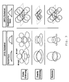
- the FIG. 3 shows a comparison of the piezoelectric fields (1st and 2nd order) of quantum dots placed on a (111) face (left) and on a (001) face (right).
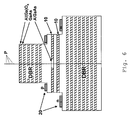
- FIG. 6 shows an exemplary embodiment of a photon pair source in a three-dimensional view. It can be seen how the quantum dot layer is embedded in a cavity. At the top and at the bottom are DBR mirrors DBR (DBR: Distributed Bragg Reflector). The oxide aperture 10 serves to manipulate the current path and thus the targeted spatial selection of individual quantum dots.
- DBR Distributed Bragg Reflector
- the embedding in a cavity makes it possible to direct the photon pairs P formed and efficiently out of the photon pair source. Similar to vertically emitting lasers, the cavity is preferably designed so that the energy of the entangled photons is in resonance with the cavity modes. Based on the Purcell effect, this increases the rate of spontaneous emission and also increases the coupling-out efficiency.
- the metal contacts are identified by the reference numeral 20.
- Such a photon pair source could, for example, form part of a photonic network for the transmission of quantum-cryptographically encrypted data, for example by means of the Eckert protocol ( A. Eckert, J. Rarity, P. Tapster, M. Palma, Phys. Rev. Lett. 69, p.1293 et seq. (1992 )).
Landscapes
- Physics & Mathematics (AREA)
- Optics & Photonics (AREA)
- Engineering & Computer Science (AREA)
- Nanotechnology (AREA)
- Chemical & Material Sciences (AREA)
- Condensed Matter Physics & Semiconductors (AREA)
- General Physics & Mathematics (AREA)
- Electromagnetism (AREA)
- Biophysics (AREA)
- Crystallography & Structural Chemistry (AREA)
- Life Sciences & Earth Sciences (AREA)
- Optical Integrated Circuits (AREA)
- Semiconductor Lasers (AREA)
- Recrystallisation Techniques (AREA)
Description
- Photonenpaarquelle und Verfahren zu deren Herstellung Die Erfindung bezieht sich auf ein Verfahren mit den Merkmalen gemäß dem Oberbegriff des Anspruchs 1.
- Ein derartiges Verfahren ist aus der Internationalen Patentanmeldung
WO 2007/062625 A2 bekannt. Bei diesem vorbekannten Verfahren wird eine verschränkte Photonenpaare erzeugende Photonenpaarquelle hergestellt, indem ein oder mehrere Quantenpunkte auf einem Substrat abgeschieden werden. Um zu erreichen, dass die Photonenpaarquelle verschränkte Photonenpaare erzeugen kann, wird die Feinstrukturaufspaltung des exzitonischen Energieniveaus des bzw. der Quantenpunkte möglichst klein eingestellt. In der genannten Druckschrift wird empfohlen, für die Feinstrukturaufspaltung einen Bereich zwischen -100 µeV und +100 µeV vorzusehen, um die Erzeugung verschränkter Photonenpaare zu ermöglichen. Erreicht wird eine solche Feinstrukturaufspaltung gemäß der Lehre der Druckschrift dadurch, dass eine Atomanzahl pro Quantenpunkt zwischen 800 und 5000 Atomen eingestellt wird. - Weitere Verfahren zur Herstellung von derartigen Photonenpaarquellen sind in "Integration of site-controlled pyramidal quantum dots and photonic crystal membrane cavities" von P. Gallo & al., Applied Physics Letters 92, 263101 (2008) und "A semiconductor source of triggered entangled photon pairs" von R.M.Stevenson & al., Nature, Vol. 439, 12.01.2006. Seiten 179-182, offenbart.
- Der Erfindung liegt die Aufgabe zugrunde, ein Verfahren zum Herstellen einer verschränkte Photonenpaare erzeugenden Photonenpaarquelle anzugeben, das sich noch einfacher und reproduzierbarer als bisherige Verfahren durchführen lässt.
- Diese Aufgabe wird erfindungsgemäß durch ein Verfahren mit den Merkmalen gemäß Patentanspruch 1 gelöst. Vorteilhafte Ausgestaltungen des erfindungsgemäßen Verfahrens sind in Unteransprüchen angegeben.
- Danach ist erfindungsgemäß vorgesehen, dass das Einstellen der Feinstrukturaufspaltung des exzitonischen Energieniveaus der Quantenpunkte dadurch erfolgt, dass diese auf einer {111}-Kristallfläche eines Halbleitersubstrats abgeschieden werden. Unter einer {111}-Kristallfläche werden die (111)-orientierte Kristallfläche des Substrats sowie alle anderen Kristallflächen verstanden, die zu der (111)-orientierten Kristallfläche äquivalent sind.
- Ein wesentlicher Vorteil des erfindungsgemäßen Verfahrens ist darin zu sehen, dass bei diesem die Feinstrukturaufspaltung stets Null, zumindest stets nahezu Null, ist. Dieser Sachverhalt wurde erfinderseitig durch theoretische Untersuchungen festgestellt, bei denen die exzitonischen Zustände der Quantenpunkte mittels der so genannten Konfigurations-Wechselwirkungsmethode (nachfolgend kurz CI-Methode genannt) berechnet wurden. Dabei wurde der Mehrteilchen-Hamilton-Operator in eine Basis aus antisymmetrisierten Produkten aus Einteilchenwellenfunktionen (Slater-Determinaten) entwickelt. Die Einteilchenzustände wurden mittels der so genannten 8-Band-k p-Theorie unter Berücksichtigung der realen 3D-Geometrie, der durch das Stranski-Krastanow Wachstumsverfahren bedingten Gitterverzerrung und der hier entscheidenden piezoelektrischen Effekte berechnet. Die aus der Quantenchemie abgeleitete CI-Methode ist sehr exakt und berücksichtigt neben den direkten Coulomb- und Korrelationseffekten auch die hier auftretenden Austauschterme. Mittels dieser Methode wurde erfinderseitig die Feinstrukturaufspaltung von auf (111)-Substrat platzierten Quantenpunkten modelliert, wobei die Quantenpunkte selbst als rotationssymmetrisch angenommen wurden. Variiert wurden das vertikale Aspektverhältnis (Verhältnis Höhe zu Breite), die Quantenpunktgröße und der mittlere Indiumanteil im Quantenpunkt. Aus Symmetrieüberlegungen konnte abgeleitet werden, dass für jeden Quantenpunkt auf einem (111)-Substrat mit einer mindestens dreizähligen Symmetrieachse senkrecht zur (111)-Ebene die Feinstrukturaufspaltung verschwinden muss. Dies deckt sich auch mit numerischen Simulationen, die erfinderseitig durchgeführt wurden. Erfinderseitig wurde dabei außerdem festgestellt, dass es aufgrund der Gittersymmetrie bei einer {111}-Kristalloberfläche keine orthogonal zueinander stehenden Anisotropierichtungen für die Ad-atom-Mobilitäten gibt, die zum Wachstum eines in lateraler Richtung elongierten Quantenpunkts führen könnte. Bei einer "perfekten" {111}-Oberfläche ist also stets mit einer C3v-Symmetrie des Quantenpunkts - d.h. der entstehende Quantenpunkt besitzt eine dreizählige Symmetrieachse - und damit mit einem Wegfall der Feinstrukturaufspaltung zu rechnen. Abweichungen davon sind ausschließlich statistischer (zufälliger) Natur und technisch zu vernachlässigen.
- Ein weiterer wesentlicher Vorteil des erfindungsgemäßen Verfahrens besteht darin, dass ein durch Verspannung des Quantenpunkts entstehendes piezoelektrisches Feld für den Quantenpunkt keine symmetriereduzierende Wirkung entfaltet und somit die C3v-Symmetrie und damit die Feinstrukturaufspaltung auch im Falle einer Verspannung und bei Auftreten eines piezoelektrischen Felds erhalten bleibt.
- Ein dritter wesentlicher Vorteil des erfindungsgemäßen Verfahrens beruht darauf, dass die Symmetrie des unterliegenden Kristallgitters des Halbleitersubstrats mit der C3v-Symmetrie des Quantenpunkts verträglich ist und demgemäß also keine symmetrieerniedrigende Wirkung entfalten kann. Aufgrund der Verwendung einer {111}-Substratfläche weist das quantenmechanische Confinement-Potential ebenfalls mindestens eine C3v-Symmetrie auf, so dass die Feinstrukturaufspaltung verschwinden muss und sich demgemäß verschränkte Photonenpaare erzeugen lassen.
- Ein weiterer wesentlicher Vorteil des erfindungsgemäßen Verfahrens ist darin zu sehen, dass sich mit diesem in sehr einfacher Weise Photonenpaarquellen für eine Dateiverschlüsselung, welche auf quantenmechanischen Prinzipien basiert, herstellen lassen. Bei verschränkten Photonenpaaren beeinflusst die Messung eines Photons direkt das Messergebnis für das andere Photon des jeweiligen Photonenpaares, selbst wenn dieses weit entfernt ist. Ein potentieller "Mithörer" müsste, um an Informationen zu gelangen, ein eigenes Messgerät in die Übertragungsleitung stellen und würde damit zwangsläufig durch seine Messung die Verschränktheit der Photonenpaare aufheben, die Photonenübertragung also verändern. Dies wiederum macht sich in den Polarisationsmessungen am Ort des Empfängers bemerkbar, so dass ein Abhören bemerkt werden kann.
- Gemäß einer bevorzugten Ausgestaltung des Verfahrens ist vorgesehen, dass das vertikale Aspektverhältnis des Quantenpunkts zwischen 0,05 und 0,7, insbesondere zwischen 0,15 und 0,5, liegt. Beispielsweise wird das Verhältnis zwischen der Höhe des Quantenpunkts und dem Durchmesser des Quantenpunkts - an der Auflagefläche auf dem Halbleitersubstrat - zwischen 0,05 und 0,7 eingestellt.
- Der zumindest eine Quantenpunkt und/oder das Halbleitersubstrat bestehen vorzugsweise aus einem Mischkristall, der aufweist:
- In(Ga)As-Material, das in einen Ga(In,Al)As-Kristall eingebaut ist,
- In(Ga)P-Material, das in einen Ga(In,Al)P-Kristall eingebaut ist,
- In(Ga)As-Material, das in einen In(Ga,Al)P-Kristall eingebaut ist, und/oder
- InxGa1-xAs-Material, wobei x zwischen 0,3 und 1 liegt.
- Der Durchmesser des Quantenpunkts - an der Auflagefläche auf dem Halbleitersubstrat - wird vorzugsweise zwischen 5 nm und 50 nm, insbesondere zwischen 10 nm und 20 nm, gewählt.
- Die Kontur des Quantenpunkts - senkrecht zur {111}-Fläche des Substrats gesehen - ist bevorzugt dreieckig, sechseckig oder rund.
- Die Erfindung bezieht sich außerdem auf eine Photonenpaarquelle zum Erzeugen verschränkter Photonenpaare mit zumindest einem Quantenpunkt.
- Erfindungsgemäß ist diesbezüglich vorgesehen, dass der zumindest eine Quantenpunkt auf einer {111}-Kristallfläche eines Halbleitersubstrats abgeschieden ist.
- Bezüglich der Vorteile der erfindungsgemäßen Photonenpaarquelle sei auf die obigen Ausführungen im Zusammenhang mit dem erfindungsgemäßen Verfahren verwiesen, da die Vorteile der erfindungsgemäßen Photonenpaarquelle denen des erfindungsgemäßen Verfahrens im Wesentlichen entsprechen.
- Vorteilhafte Ausgestaltungen der Photonenpaarquelle sind in Unteransprüchen angegeben.
- Die Erfindung wird nachfolgend anhand von Ausführungsbeispielen näher erläutert; dabei zeigen beispielhaft
-
Fig. 1 ein schematisches Energiediagramm, -
Fig. 2 einen Vergleich zwischen der Photonenstatistik verschiedener Photonenquellen, -
Fig. 3 piezoelektrische Felder im Vergleich, -
Fig. 4 eine (001)- und eine (111)-Substratorientierung, -
Fig. 5 Bindungsenergien im Vergleich und -
Fig. 6 ein Ausführungsbeispiel für eine erfindungsgemäße Photonenpaarquelle. - In der
Figur 1 ist zur allgemeinen Erläuterung ein schematisches Energiediagramm für ein Exziton (X) und ein Biexziton (XX) in einem Quantenpunkt dargestellt. Man erkennt die Feinstrukturaufspaltung FSS des exzitonischen Zustandes, die sich zu EX1 - EX2 ergibt. Die beiden senkrecht aufeinander stehenden Polarisationsrichtungen sind mit den Bezugszeichen π+ und π- bezeichnet. Eine Emission verschränkter Photonenpaare lässt sich erreichen, wenn die Feinstrukturaufspaltung FSS möglich klein ist, also beispielsweise zwischen -100 µeV und +100 µeV liegt. Es werden hierzu Photonen aus der Biexziton → Exziton → 0 Zerfallskaskade verwendet. Ein zu großer energetischer Abstand zwischen den zwei vorhandenen exzitonischen Zuständen würde die Verschränktheit der emittierten Photonenpaare verhindern. - Die
Figur 2 zeigt zur allgemeinen Erläuterung einen Vergleich zwischen der Photonenstatistik einer klassischen Photonenquelle, die nach der Poisson-Statistik
- Die
Figur 3 zeigt einen Vergleich der piezoelektrischen Felder (1. und 2. Ordnung) von Quantenpunkten, die auf einer (111)-Fläche (links) und auf einer (001)-Fläche (rechts) platziert wurden. Man erkennt die unterschiedliche Ausgestaltung der piezoelektrischen Felder, die dazu führt, dass bei einem Wachstum eines Quantenpunkts auf einer (111)-Fläche die Feinstrukturaufspaltung stets Null beträgt, und die auch dazu führt, dass sich bei einem Wachstum auf einer (001)-Fläche eine Feinstrukturaufspaltung von Null nur sehr schwer erreichen lässt. - In der
Figur 4 sind zur allgemeinen Erläuterung die (001)-und die (111)-Kristallorientierung nochmals in einer dreidimensionalen Darstellung gezeigt. - In der
Figur 5 sind für Ausführungsbeispiele von Photonenpaarquellen die Bindungsenergien des Biexzitons (gestrichelte, gekrümmte Linie) relativ zum Exziton (auf 0 gesetzt, durchgehende Linie bei 0 meV) gezeigt. Man erkennt, dass sich die Differenz zwischen der Biexzitonübergangsenergie und der Exzitonübergangsenergie, also die Biexzitonbindungsenergie, bei konstanter Feinstrukturaufspaltung gleich Null durch geeignete Parameterwahl der Quantenpunkte beeinflussen lässt. DieFig. 5 zeigt die Bindungsenergien für folgende Fälle: - (a) Für den Fall der Variation der Quantenpunktgröße, von 10,2 nm bis 20,4 nm Durchmesser. Das vertikale Aspektverhältnis beträgt 0,17.
- (b) Für den Fall der Variation des vertikalen Aspektverhältnisses zwischen 0,17 und 0,5 bei konstantem Volumen. Der Durchmesser der flachsten Struktur beträgt hier beispielsweise 17,0 nm.
- (c) Für den Fall der Variation des Gehaltes von InAs im Quantenpunkt zwischen 100% (0% GaAs) und 30% (70% GaAs). Diejenige Quantenpunktstruktur, die in allen drei Serien gemeinsam auftaucht, ist jeweils mit einem Pfeil gekennzeichnet.
- Die Quantenpunktgröße, das vertikale Aspektverhältnis und die chemische Komposition des Systems werden vorzugsweise als Parameter verwendet, um optimale Eigenschaften der Photonenpaarquellen nach den jeweiligen Einsatzanforderungen zu erreichen. Folgende Parameter, einzeln oder in Kombination, sind als vorteilhaft anzusehen:
- Das vertikale Aspektverhältnis der Quantenpunkte liegt zwischen 0,05 und 0,7, insbesondere zwischen 0,15 und 0,5.
- Das Verhältnis zwischen der Höhe der Quantenpunkte und dem Durchmesser der Quantenpunkte liegt zwischen 0,05 und 0,7.
- Der Durchmesser der Quantenpunkte liegt zwischen 5 nm und 50 nm, insbesondere zwischen 10 nm und 20 nm.
- Die Quantenpunkte weisen eine dreieckige, sechseckige oder runde Kontur auf.
- Das Substrat und/oder die Quantenpunkte bestehen aus einem Mischkristall, der aufweist:
- In(Ga)As-Material, das in einen Ga(In,Al)As-Kristall eingebaut ist, und/oder
- In(Ga)P-Material, das in einen Ga(In,Al)P-Kristall eingebaut ist, und/oder
- In(Ga)As-Material, das in einen In(Ga,Al)P-Kristall eingebaut ist, und/oder
- InxGa1-xAs-Material, wobei x zwischen 0,3 und 1 liegt.
- Die
Figur 6 zeigt ein Ausführungsbeispiel für eine Photonenpaarquelle in einer dreidimensionalen Sicht. Man erkennt, wie die Quantenpunktschicht in eine Kavität eingebettet ist. Am oberen sowie am unteren Ende befinden sich DBR-Spiegel DBR (DBR: Distributed Bragg Reflector = verteilter Bragg-Reflektor). Die Oxidapertur 10 dient zur Manipulation des Strompfades und damit der zielgerichteten räumlichen Selektion von einzelnen Quantenpunkten. - Die Einbettung in eine Kavität ermöglicht es, die entstehenden Photonenpaare P gerichtet und effizient aus der Photonenpaarquelle auszukoppeln. Ähnlich wie bei vertikal emittierenden Lasern ist die Kavität vorzugsweise so ausgestaltet, dass die Energie der verschränkten Photonen in Resonanz mit den Kavitätsmoden ist. Basierend auf dem Purcell-Effekt wird damit die Rate der spontanen Emission hinaufgesetzt und zudem die Auskopplungseffizienz erhöht. Die Metallkontakte sind mit dem Bezugszeichen 20 gekennzeichnet.
- Eine solche Photonenpaarquelle könnte beispielsweise einen Bestandteil eines photonischen Netzes zur Übermittlung quantenkryptographisch verschlüsselter Daten bilden, z.B. mittels des Eckert-Protokolls (A. Eckert, J. Rarity, P. Tapster, M. Palma, Phys. Rev. Lett.69, S.1293 ff (1992)).
Claims (14)
- Verfahren zum Herstellen einer verschränkte Photonenpaare erzeugenden Photonenpaarquelle mit mindestens einem Quantenpunkt, wobei bei dem Verfahren das Betriebsverhalten der Photonenpaarquelle durch ein Einstellen der Feinstrukturaufspaltung des exzitonischen Energieniveaus des zumindest einen Quantenpunkts festgelegt wird,
dadurch gekennzeichnet, dass
das Einstellen der Feinstrukturaufspaltung des exzitonischen Energieniveaus dadurch erfolgt, dass der zumindest eine Quantenpunkt auf einer {111}-Kristallfläche eines Halbleitersubstrats abgeschieden wird. - Verfahren nach Anspruch 1,
dadurch gekennzeichnet, dass
ein vertikales Aspektverhältnis des Quantenpunkts zwischen 0,05 und 0,7, insbesondere zwischen 0,15 und 0,5, hergestellt wird. - Verfahren nach einem der vorangehenden Ansprüche,
dadurch gekennzeichnet, dass
das Verhältnis zwischen der Höhe des Quantenpunkts und dem Durchmesser des Quantenpunkts - an der Auflagefläche auf dem Halbleitersubstrat - zwischen 0,05 und 0,7 eingestellt wird. - Verfahren nach einem der vorangehenden Ansprüche 1-3,
dadurch gekennzeichnet, dass
der zumindest eine Quantenpunkt aus einem Mischkristall hergestellt wird, wobei der Mischkristall In(Ga)As-Material aufweist, das in einen Ga(In,Al)As-Kristall eingebaut ist. - Verfahren nach einem der vorangehenden Ansprüche 1-3,
dadurch gekennzeichnet, dass
der zumindest eine Quantenpunkt aus einem Mischkristall hergestellt wird, wobei der Mischkristall In(Ga)P-Material aufweist, das in einen Ga(In,Al)P-Kristall eingebaut ist. - Verfahren nach einem der vorangehenden Ansprüche 1-3,
dadurch gekennzeichnet, dass
der zumindest eine Quantenpunkt aus einem Mischkristall hergestellt wird, wobei der Mischkristall In(Ga)As-Material aufweist, das in einen In(Ga,Al)P-Kristall eingebaut ist. - Verfahren nach einem der vorangehenden Ansprüche 1-3,
dadurch gekennzeichnet, dass
der zumindest eine Quantenpunkt aus einem Mischkristall mit InxGa1-xAs-Material, wobei x zwischen 0,3 und 1 liegt, hergestellt wird. - Verfahren nach einem der vorangehenden Ansprüche,
dadurch gekennzeichnet, dass
der Quantenpunkt mit einem Durchmesser - an der Auflagefläche auf dem Halbleitersubstrat - zwischen 5 nm und 50 nm, insbesondere zwischen 10 nm und 20 nm, hergestellt wird. - Verfahren nach einem der vorangehenden Ansprüche,
dadurch gekennzeichnet, dass
der Quantenpunkt mit einer dreieckigen, sechseckigen oder runden Kontur, insbesondere senkrecht zur {111}-Fläche des Substrats gesehen, hergestellt wird. - Photonenpaarquelle zum Erzeugen verschränkter Photonenpaare mit zumindest einem Quantenpunkt,
dadurch gekennzeichnet, dass
der zumindest eine Quantenpunkt auf einer {111}-Kristallfläche eines Halbleitersubstrats abgeschieden ist. - Photonenpaarquelle nach Anspruch 10,
dadurch gekennzeichnet, dass
das Verhältnis zwischen der Höhe des Quantenpunkts und dem Durchmesser des Quantenpunkts - an der Auflagefläche auf der {111}-Kristallfläche des Halbleitersubstrats - zwischen 0,05 und 0,7, insbesondere zwischen 0,15 und 0,5, liegt. - Photonenpaarquelle nach einem der vorangehenden Ansprüche 10-11,
dadurch gekennzeichnet, dass
der zumindest eine Quantenpunkt und/oder das Halbleitersubstrat aus einem Mischkristall besteht, der aufweist:- In(Ga)As-Material, das in einen Ga(In,Al)As-Kristall eingebaut ist, und/oder- In(Ga)P-Material, das in einen Ga(In,Al)P-Kristall eingebaut ist, und/oder- In(Ga)As-Material, das in einen In(Ga,Al)P-Kristall eingebaut ist, und/oder- InxGa1-xAs-Material, wobei x zwischen 0,3 und 1 liegt. - Photonenpaarquelle nach einem der vorangehenden Ansprüche 10-12,
dadurch gekennzeichnet, dass
der Durchmesser des Quantenpunkts - an der Auflagefläche auf der {111}-Kristallfläche des Halbleitersubstrats - zwischen 5 nm und 50 nm, insbesondere zwischen 10 nm und 20 nm, beträgt. - Photonenpaarquelle nach einem der vorangehenden Ansprüche 10-13,
dadurch gekennzeichnet, dass
der Quantenpunkt eine dreieckige, sechseckige oder runde Kontur, insbesondere senkrecht zur {111}-Fläche des Halbleitersubstrats gesehen, aufweist.
Applications Claiming Priority (2)
| Application Number | Priority Date | Filing Date | Title |
|---|---|---|---|
| DE102008036400A DE102008036400B3 (de) | 2008-08-01 | 2008-08-01 | Photonenpaarquelle und Verfahren zu deren Herstellung |
| PCT/DE2009/001025 WO2010012268A2 (de) | 2008-08-01 | 2009-07-20 | Photonenpaarquelle und verfahren zu deren herstellung |
Publications (2)
| Publication Number | Publication Date |
|---|---|
| EP2308143A2 EP2308143A2 (de) | 2011-04-13 |
| EP2308143B1 true EP2308143B1 (de) | 2016-10-26 |
Family
ID=41427526
Family Applications (1)
| Application Number | Title | Priority Date | Filing Date |
|---|---|---|---|
| EP09775999.7A Not-in-force EP2308143B1 (de) | 2008-08-01 | 2009-07-20 | Photonenpaarquelle und verfahren zu deren herstellung |
Country Status (7)
| Country | Link |
|---|---|
| US (1) | US8559479B2 (de) |
| EP (1) | EP2308143B1 (de) |
| JP (1) | JP2011530160A (de) |
| KR (1) | KR20110036946A (de) |
| CN (1) | CN102113188B (de) |
| DE (1) | DE102008036400B3 (de) |
| WO (1) | WO2010012268A2 (de) |
Families Citing this family (13)
| Publication number | Priority date | Publication date | Assignee | Title |
|---|---|---|---|---|
| GB2476926B (en) | 2009-11-06 | 2012-05-02 | Toshiba Res Europ Ltd | Tuneable quantum light source |
| GB2479162B (en) * | 2010-03-30 | 2013-05-15 | Toshiba Res Europ Ltd | A quantum logic component and a method of controlling a qubit |
| US8149888B1 (en) | 2010-09-27 | 2012-04-03 | Technische Universitat Berlin | Single photon source |
| GB2488199B (en) * | 2012-01-23 | 2013-02-06 | Toshiba Res Europ Ltd | Tuneable quantum light source |
| CN103346266B (zh) * | 2013-06-21 | 2016-03-30 | 深圳市华星光电技术有限公司 | 一种发光器件、显示面板及其制造方法 |
| CA2978360C (en) | 2015-03-19 | 2023-09-19 | Institut National De La Recherche Scientifique | Passive mode-locked laser system and method for generation of long pulses |
| GB2549703B (en) * | 2016-04-19 | 2019-11-06 | Toshiba Kk | An optical device and method for its fabrication |
| WO2019014870A1 (zh) * | 2017-07-19 | 2019-01-24 | 华为技术有限公司 | 量子计算装置及光子量子逻辑门的实现方法 |
| CN108832484B (zh) * | 2018-05-08 | 2020-04-28 | 天津大学 | 一种增强关联光子对源性能的方法 |
| CN110098563B (zh) * | 2019-06-11 | 2021-03-12 | 中国科学院半导体研究所 | 基于双腔结构的纠缠光源 |
| US11829050B2 (en) * | 2021-11-22 | 2023-11-28 | Electronics And Telecommunications Research Institute | Entangled-photon pair emitting device |
| CN114430142B (zh) * | 2022-04-01 | 2022-07-15 | 中国科学技术大学 | 产生纠缠光子对的器件及其制作方法 |
| CN121986299A (zh) * | 2023-10-09 | 2026-05-05 | 弗劳恩霍夫应用研究促进协会 | 用于产生纠缠光子的方法 |
Family Cites Families (6)
| Publication number | Priority date | Publication date | Assignee | Title |
|---|---|---|---|---|
| CN1027204C (zh) * | 1992-09-19 | 1994-12-28 | 南京大学 | 可见光致发光的硅量子点制备方法 |
| KR100486607B1 (ko) * | 2002-09-17 | 2005-05-03 | 주식회사 하이닉스반도체 | 양자점 형성 방법 |
| US7998807B2 (en) * | 2003-08-22 | 2011-08-16 | The Board Of Trustees Of The University Of Illinois | Method for increasing the speed of a light emitting biopolar transistor device |
| JP2005136267A (ja) * | 2003-10-31 | 2005-05-26 | Fujitsu Ltd | 半導体量子ドット素子 |
| JP2006267888A (ja) * | 2005-03-25 | 2006-10-05 | Nippon Telegr & Teleph Corp <Ntt> | 半導体光制御素子 |
| DE102005057800B4 (de) * | 2005-11-30 | 2009-02-26 | Technische Universität Berlin | Einzelphotonenquelle und Verfahren zu deren Herstellung und Betrieb |
-
2008
- 2008-08-01 DE DE102008036400A patent/DE102008036400B3/de not_active Expired - Fee Related
-
2009
- 2009-07-20 US US13/056,967 patent/US8559479B2/en not_active Expired - Fee Related
- 2009-07-20 CN CN2009801299681A patent/CN102113188B/zh not_active Expired - Fee Related
- 2009-07-20 EP EP09775999.7A patent/EP2308143B1/de not_active Not-in-force
- 2009-07-20 KR KR1020117004630A patent/KR20110036946A/ko not_active Withdrawn
- 2009-07-20 WO PCT/DE2009/001025 patent/WO2010012268A2/de not_active Ceased
- 2009-07-20 JP JP2011520321A patent/JP2011530160A/ja active Pending
Also Published As
| Publication number | Publication date |
|---|---|
| WO2010012268A2 (de) | 2010-02-04 |
| DE102008036400B3 (de) | 2010-01-21 |
| WO2010012268A3 (de) | 2010-04-15 |
| CN102113188A (zh) | 2011-06-29 |
| KR20110036946A (ko) | 2011-04-12 |
| JP2011530160A (ja) | 2011-12-15 |
| US8559479B2 (en) | 2013-10-15 |
| EP2308143A2 (de) | 2011-04-13 |
| US20110142088A1 (en) | 2011-06-16 |
| CN102113188B (zh) | 2013-05-29 |
Similar Documents
| Publication | Publication Date | Title |
|---|---|---|
| DE102008036400B3 (de) | Photonenpaarquelle und Verfahren zu deren Herstellung | |
| DE69418986T2 (de) | Abstimmen des Bandabstands einer halbleitenden Quantumwell-Struktur | |
| EP1883140B1 (de) | LD oder LED mit Übergitter-Mantelschicht und Dotierungsgradienten | |
| DE69412738T2 (de) | Verspannte Quantumwellstruktur mit variabler Polarisationsabhängigkeit und optische Vorrichtung mit dieser verspannten Quantumwellstruktur | |
| DE102005057800B4 (de) | Einzelphotonenquelle und Verfahren zu deren Herstellung und Betrieb | |
| DE69222617T2 (de) | Nicht-lineare optische Vorrichtung | |
| EP1630915A2 (de) | Strahlungsemittierendes optoelektronisches Bauelement mit einer Quantentopfstruktur und Verfahren zu dessen Herstellung | |
| DE60313140T2 (de) | Quanten-nanozusammensetzungshalbleiterlaser und quanten-nanozusammensetzungsarray | |
| DE112016003950T5 (de) | Oberflächenemittierender laser mit zweidimensionalem photonischen kristall | |
| DE60109179T2 (de) | Quantenkaskadierter laser | |
| DE112007000664T5 (de) | Zweidimensionaler photonischer Kristall | |
| DE69225056T2 (de) | Vorrichtung mit Halbleiterkörper und Mitteln zur Modulation der optischen Transparenz desselben | |
| DE112016007396T5 (de) | Sättigbarer Absorptionsspiegel aus Verbundstruktur | |
| DE102008040374A1 (de) | Lasereinrichtung | |
| DE102020108941B4 (de) | Diodenlaser mit verrringerter Strahldivergenz | |
| DE3700909A1 (de) | Verfahren zur herstellung eines halbleiterelementes mit verketteter rueckkopplung | |
| DE102006010277A1 (de) | Halbleitervorrichtung | |
| DE69616237T2 (de) | Halbleiter-laserdiode und deren herstellungsverfahren | |
| DE69201283T2 (de) | Halbleiterlaser. | |
| DE102012007793B4 (de) | Verfahren und Vorrichtung zur Erzeugung einer kontrollierbaren Einzelphoton-Emission | |
| DE102007046752B4 (de) | Quasisubstrat für ein optoelektronisches Bauelement und optoelektronisches Bauelement | |
| EP3694005B1 (de) | Vorrichtung und verfahren zur erzeugung einer einzelphotonenemission | |
| DE10335443B4 (de) | Quantentopfstruktur | |
| WO2021047736A1 (de) | Optisch aktiver und durch gatter definierter quantenpunkt | |
| DE102023117613B3 (de) | Optoelektronische Nanostruktur, Verfahren zur Strahlungskonversion sowie Verfahren zur Herstellung asymmetrischer Doppel-Quantenpunkte |
Legal Events
| Date | Code | Title | Description |
|---|---|---|---|
| PUAI | Public reference made under article 153(3) epc to a published international application that has entered the european phase |
Free format text: ORIGINAL CODE: 0009012 |
|
| 17P | Request for examination filed |
Effective date: 20110301 |
|
| AK | Designated contracting states |
Kind code of ref document: A2 Designated state(s): AT BE BG CH CY CZ DE DK EE ES FI FR GB GR HR HU IE IS IT LI LT LU LV MC MK MT NL NO PL PT RO SE SI SK SM TR |
|
| AX | Request for extension of the european patent |
Extension state: AL BA RS |
|
| DAX | Request for extension of the european patent (deleted) | ||
| RIC1 | Information provided on ipc code assigned before grant |
Ipc: H01S 5/183 20060101ALI20160422BHEP Ipc: H01S 5/34 20060101AFI20160422BHEP Ipc: B82Y 20/00 20110101ALI20160422BHEP Ipc: H01S 5/10 20060101ALI20160422BHEP Ipc: H01S 5/32 20060101ALI20160422BHEP |
|
| GRAP | Despatch of communication of intention to grant a patent |
Free format text: ORIGINAL CODE: EPIDOSNIGR1 |
|
| INTG | Intention to grant announced |
Effective date: 20160603 |
|
| GRAS | Grant fee paid |
Free format text: ORIGINAL CODE: EPIDOSNIGR3 |
|
| GRAA | (expected) grant |
Free format text: ORIGINAL CODE: 0009210 |
|
| AK | Designated contracting states |
Kind code of ref document: B1 Designated state(s): AT BE BG CH CY CZ DE DK EE ES FI FR GB GR HR HU IE IS IT LI LT LU LV MC MK MT NL NO PL PT RO SE SI SK SM TR |
|
| REG | Reference to a national code |
Ref country code: GB Ref legal event code: FG4D Free format text: NOT ENGLISH |
|
| REG | Reference to a national code |
Ref country code: CH Ref legal event code: EP |
|
| REG | Reference to a national code |
Ref country code: AT Ref legal event code: REF Ref document number: 840633 Country of ref document: AT Kind code of ref document: T Effective date: 20161115 |
|
| REG | Reference to a national code |
Ref country code: IE Ref legal event code: FG4D Free format text: LANGUAGE OF EP DOCUMENT: GERMAN |
|
| REG | Reference to a national code |
Ref country code: CH Ref legal event code: NV Representative=s name: PETER RUTZ, CH Ref country code: DE Ref legal event code: R096 Ref document number: 502009013283 Country of ref document: DE |
|
| REG | Reference to a national code |
Ref country code: LT Ref legal event code: MG4D |
|
| PG25 | Lapsed in a contracting state [announced via postgrant information from national office to epo] |
Ref country code: LV Free format text: LAPSE BECAUSE OF FAILURE TO SUBMIT A TRANSLATION OF THE DESCRIPTION OR TO PAY THE FEE WITHIN THE PRESCRIBED TIME-LIMIT Effective date: 20161026 |
|
| REG | Reference to a national code |
Ref country code: NL Ref legal event code: MP Effective date: 20161026 |
|
| PG25 | Lapsed in a contracting state [announced via postgrant information from national office to epo] |
Ref country code: SE Free format text: LAPSE BECAUSE OF FAILURE TO SUBMIT A TRANSLATION OF THE DESCRIPTION OR TO PAY THE FEE WITHIN THE PRESCRIBED TIME-LIMIT Effective date: 20161026 Ref country code: GR Free format text: LAPSE BECAUSE OF FAILURE TO SUBMIT A TRANSLATION OF THE DESCRIPTION OR TO PAY THE FEE WITHIN THE PRESCRIBED TIME-LIMIT Effective date: 20170127 Ref country code: NO Free format text: LAPSE BECAUSE OF FAILURE TO SUBMIT A TRANSLATION OF THE DESCRIPTION OR TO PAY THE FEE WITHIN THE PRESCRIBED TIME-LIMIT Effective date: 20170126 Ref country code: LT Free format text: LAPSE BECAUSE OF FAILURE TO SUBMIT A TRANSLATION OF THE DESCRIPTION OR TO PAY THE FEE WITHIN THE PRESCRIBED TIME-LIMIT Effective date: 20161026 |
|
| PG25 | Lapsed in a contracting state [announced via postgrant information from national office to epo] |
Ref country code: HR Free format text: LAPSE BECAUSE OF FAILURE TO SUBMIT A TRANSLATION OF THE DESCRIPTION OR TO PAY THE FEE WITHIN THE PRESCRIBED TIME-LIMIT Effective date: 20161026 Ref country code: PL Free format text: LAPSE BECAUSE OF FAILURE TO SUBMIT A TRANSLATION OF THE DESCRIPTION OR TO PAY THE FEE WITHIN THE PRESCRIBED TIME-LIMIT Effective date: 20161026 Ref country code: IS Free format text: LAPSE BECAUSE OF FAILURE TO SUBMIT A TRANSLATION OF THE DESCRIPTION OR TO PAY THE FEE WITHIN THE PRESCRIBED TIME-LIMIT Effective date: 20170226 Ref country code: NL Free format text: LAPSE BECAUSE OF FAILURE TO SUBMIT A TRANSLATION OF THE DESCRIPTION OR TO PAY THE FEE WITHIN THE PRESCRIBED TIME-LIMIT Effective date: 20161026 Ref country code: ES Free format text: LAPSE BECAUSE OF FAILURE TO SUBMIT A TRANSLATION OF THE DESCRIPTION OR TO PAY THE FEE WITHIN THE PRESCRIBED TIME-LIMIT Effective date: 20161026 Ref country code: FI Free format text: LAPSE BECAUSE OF FAILURE TO SUBMIT A TRANSLATION OF THE DESCRIPTION OR TO PAY THE FEE WITHIN THE PRESCRIBED TIME-LIMIT Effective date: 20161026 Ref country code: PT Free format text: LAPSE BECAUSE OF FAILURE TO SUBMIT A TRANSLATION OF THE DESCRIPTION OR TO PAY THE FEE WITHIN THE PRESCRIBED TIME-LIMIT Effective date: 20170227 |
|
| REG | Reference to a national code |
Ref country code: FR Ref legal event code: PLFP Year of fee payment: 9 |
|
| REG | Reference to a national code |
Ref country code: DE Ref legal event code: R097 Ref document number: 502009013283 Country of ref document: DE |
|
| PG25 | Lapsed in a contracting state [announced via postgrant information from national office to epo] |
Ref country code: CZ Free format text: LAPSE BECAUSE OF FAILURE TO SUBMIT A TRANSLATION OF THE DESCRIPTION OR TO PAY THE FEE WITHIN THE PRESCRIBED TIME-LIMIT Effective date: 20161026 Ref country code: RO Free format text: LAPSE BECAUSE OF FAILURE TO SUBMIT A TRANSLATION OF THE DESCRIPTION OR TO PAY THE FEE WITHIN THE PRESCRIBED TIME-LIMIT Effective date: 20161026 Ref country code: DK Free format text: LAPSE BECAUSE OF FAILURE TO SUBMIT A TRANSLATION OF THE DESCRIPTION OR TO PAY THE FEE WITHIN THE PRESCRIBED TIME-LIMIT Effective date: 20161026 Ref country code: EE Free format text: LAPSE BECAUSE OF FAILURE TO SUBMIT A TRANSLATION OF THE DESCRIPTION OR TO PAY THE FEE WITHIN THE PRESCRIBED TIME-LIMIT Effective date: 20161026 Ref country code: SK Free format text: LAPSE BECAUSE OF FAILURE TO SUBMIT A TRANSLATION OF THE DESCRIPTION OR TO PAY THE FEE WITHIN THE PRESCRIBED TIME-LIMIT Effective date: 20161026 |
|
| PG25 | Lapsed in a contracting state [announced via postgrant information from national office to epo] |
Ref country code: SM Free format text: LAPSE BECAUSE OF FAILURE TO SUBMIT A TRANSLATION OF THE DESCRIPTION OR TO PAY THE FEE WITHIN THE PRESCRIBED TIME-LIMIT Effective date: 20161026 Ref country code: BG Free format text: LAPSE BECAUSE OF FAILURE TO SUBMIT A TRANSLATION OF THE DESCRIPTION OR TO PAY THE FEE WITHIN THE PRESCRIBED TIME-LIMIT Effective date: 20170126 Ref country code: IT Free format text: LAPSE BECAUSE OF FAILURE TO SUBMIT A TRANSLATION OF THE DESCRIPTION OR TO PAY THE FEE WITHIN THE PRESCRIBED TIME-LIMIT Effective date: 20161026 |
|
| PLBE | No opposition filed within time limit |
Free format text: ORIGINAL CODE: 0009261 |
|
| STAA | Information on the status of an ep patent application or granted ep patent |
Free format text: STATUS: NO OPPOSITION FILED WITHIN TIME LIMIT |
|
| 26N | No opposition filed |
Effective date: 20170727 |
|
| PG25 | Lapsed in a contracting state [announced via postgrant information from national office to epo] |
Ref country code: SI Free format text: LAPSE BECAUSE OF FAILURE TO SUBMIT A TRANSLATION OF THE DESCRIPTION OR TO PAY THE FEE WITHIN THE PRESCRIBED TIME-LIMIT Effective date: 20161026 |
|
| REG | Reference to a national code |
Ref country code: IE Ref legal event code: MM4A |
|
| PG25 | Lapsed in a contracting state [announced via postgrant information from national office to epo] |
Ref country code: IE Free format text: LAPSE BECAUSE OF NON-PAYMENT OF DUE FEES Effective date: 20170720 |
|
| REG | Reference to a national code |
Ref country code: BE Ref legal event code: MM Effective date: 20170731 |
|
| PG25 | Lapsed in a contracting state [announced via postgrant information from national office to epo] |
Ref country code: LU Free format text: LAPSE BECAUSE OF NON-PAYMENT OF DUE FEES Effective date: 20170720 |
|
| REG | Reference to a national code |
Ref country code: FR Ref legal event code: PLFP Year of fee payment: 10 |
|
| PG25 | Lapsed in a contracting state [announced via postgrant information from national office to epo] |
Ref country code: BE Free format text: LAPSE BECAUSE OF NON-PAYMENT OF DUE FEES Effective date: 20170731 |
|
| REG | Reference to a national code |
Ref country code: CH Ref legal event code: PCAR Free format text: NEW ADDRESS: ALPENSTRASSE 14 POSTFACH 7627, 6302 ZUG (CH) |
|
| PG25 | Lapsed in a contracting state [announced via postgrant information from national office to epo] |
Ref country code: MT Free format text: LAPSE BECAUSE OF FAILURE TO SUBMIT A TRANSLATION OF THE DESCRIPTION OR TO PAY THE FEE WITHIN THE PRESCRIBED TIME-LIMIT Effective date: 20161026 |
|
| PG25 | Lapsed in a contracting state [announced via postgrant information from national office to epo] |
Ref country code: HU Free format text: LAPSE BECAUSE OF FAILURE TO SUBMIT A TRANSLATION OF THE DESCRIPTION OR TO PAY THE FEE WITHIN THE PRESCRIBED TIME-LIMIT; INVALID AB INITIO Effective date: 20090720 Ref country code: MC Free format text: LAPSE BECAUSE OF FAILURE TO SUBMIT A TRANSLATION OF THE DESCRIPTION OR TO PAY THE FEE WITHIN THE PRESCRIBED TIME-LIMIT Effective date: 20161026 |
|
| PG25 | Lapsed in a contracting state [announced via postgrant information from national office to epo] |
Ref country code: CY Free format text: LAPSE BECAUSE OF NON-PAYMENT OF DUE FEES Effective date: 20161026 |
|
| PG25 | Lapsed in a contracting state [announced via postgrant information from national office to epo] |
Ref country code: MK Free format text: LAPSE BECAUSE OF FAILURE TO SUBMIT A TRANSLATION OF THE DESCRIPTION OR TO PAY THE FEE WITHIN THE PRESCRIBED TIME-LIMIT Effective date: 20161026 |
|
| PG25 | Lapsed in a contracting state [announced via postgrant information from national office to epo] |
Ref country code: TR Free format text: LAPSE BECAUSE OF FAILURE TO SUBMIT A TRANSLATION OF THE DESCRIPTION OR TO PAY THE FEE WITHIN THE PRESCRIBED TIME-LIMIT Effective date: 20161026 |
|
| PGFP | Annual fee paid to national office [announced via postgrant information from national office to epo] |
Ref country code: AT Payment date: 20210720 Year of fee payment: 13 |
|
| PGFP | Annual fee paid to national office [announced via postgrant information from national office to epo] |
Ref country code: CH Payment date: 20210723 Year of fee payment: 13 |
|
| PGFP | Annual fee paid to national office [announced via postgrant information from national office to epo] |
Ref country code: GB Payment date: 20220725 Year of fee payment: 14 Ref country code: DE Payment date: 20220621 Year of fee payment: 14 |
|
| PGFP | Annual fee paid to national office [announced via postgrant information from national office to epo] |
Ref country code: FR Payment date: 20220725 Year of fee payment: 14 |
|
| REG | Reference to a national code |
Ref country code: CH Ref legal event code: PL |
|
| REG | Reference to a national code |
Ref country code: AT Ref legal event code: MM01 Ref document number: 840633 Country of ref document: AT Kind code of ref document: T Effective date: 20220720 |
|
| PG25 | Lapsed in a contracting state [announced via postgrant information from national office to epo] |
Ref country code: LI Free format text: LAPSE BECAUSE OF NON-PAYMENT OF DUE FEES Effective date: 20220731 Ref country code: CH Free format text: LAPSE BECAUSE OF NON-PAYMENT OF DUE FEES Effective date: 20220731 Ref country code: AT Free format text: LAPSE BECAUSE OF NON-PAYMENT OF DUE FEES Effective date: 20220720 |
|
| REG | Reference to a national code |
Ref country code: DE Ref legal event code: R119 Ref document number: 502009013283 Country of ref document: DE |
|
| GBPC | Gb: european patent ceased through non-payment of renewal fee |
Effective date: 20230720 |
|
| PG25 | Lapsed in a contracting state [announced via postgrant information from national office to epo] |
Ref country code: DE Free format text: LAPSE BECAUSE OF NON-PAYMENT OF DUE FEES Effective date: 20240201 Ref country code: GB Free format text: LAPSE BECAUSE OF NON-PAYMENT OF DUE FEES Effective date: 20230720 |
|
| PG25 | Lapsed in a contracting state [announced via postgrant information from national office to epo] |
Ref country code: FR Free format text: LAPSE BECAUSE OF NON-PAYMENT OF DUE FEES Effective date: 20230731 |