EP2306628A1 - High-efficiency, switched-capacitor power conversion - Google Patents
High-efficiency, switched-capacitor power conversion Download PDFInfo
- Publication number
- EP2306628A1 EP2306628A1 EP10171642A EP10171642A EP2306628A1 EP 2306628 A1 EP2306628 A1 EP 2306628A1 EP 10171642 A EP10171642 A EP 10171642A EP 10171642 A EP10171642 A EP 10171642A EP 2306628 A1 EP2306628 A1 EP 2306628A1
- Authority
- EP
- European Patent Office
- Prior art keywords
- capacitor
- voltage
- coupled
- output
- phase
- Prior art date
- Legal status (The legal status is an assumption and is not a legal conclusion. Google has not performed a legal analysis and makes no representation as to the accuracy of the status listed.)
- Withdrawn
Links
Images


Classifications
-
- H—ELECTRICITY
- H02—GENERATION; CONVERSION OR DISTRIBUTION OF ELECTRIC POWER
- H02J—ELECTRIC POWER NETWORKS; CIRCUIT ARRANGEMENTS OR SYSTEMS FOR SUPPLYING OR DISTRIBUTING ELECTRIC POWER; SYSTEMS FOR STORING ELECTRIC ENERGY
- H02J7/00—Circuit arrangements for charging or discharging batteries or for supplying loads from batteries
- H02J7/50—Circuit arrangements for charging or discharging batteries or for supplying loads from batteries acting upon multiple batteries simultaneously or sequentially
- H02J7/52—Circuit arrangements for charging or discharging batteries or for supplying loads from batteries acting upon multiple batteries simultaneously or sequentially for charge balancing, e.g. equalisation of charge between batteries
-
- H—ELECTRICITY
- H02—GENERATION; CONVERSION OR DISTRIBUTION OF ELECTRIC POWER
- H02M—APPARATUS FOR CONVERSION BETWEEN AC AND AC, BETWEEN AC AND DC, OR BETWEEN DC AND DC, AND FOR USE WITH MAINS OR SIMILAR POWER SUPPLY SYSTEMS; CONVERSION OF DC OR AC INPUT POWER INTO SURGE OUTPUT POWER; CONTROL OR REGULATION THEREOF
- H02M3/00—Conversion of DC power input into DC power output
- H02M3/02—Conversion of DC power input into DC power output without intermediate conversion into AC
- H02M3/04—Conversion of DC power input into DC power output without intermediate conversion into AC by static converters
- H02M3/06—Conversion of DC power input into DC power output without intermediate conversion into AC by static converters using resistors or capacitors, e.g. potential divider
- H02M3/07—Conversion of DC power input into DC power output without intermediate conversion into AC by static converters using resistors or capacitors, e.g. potential divider using capacitors charged and discharged alternately by semiconductor devices with control electrode, e.g. charge pumps
-
- H—ELECTRICITY
- H02—GENERATION; CONVERSION OR DISTRIBUTION OF ELECTRIC POWER
- H02J—ELECTRIC POWER NETWORKS; CIRCUIT ARRANGEMENTS OR SYSTEMS FOR SUPPLYING OR DISTRIBUTING ELECTRIC POWER; SYSTEMS FOR STORING ELECTRIC ENERGY
- H02J2207/00—Details of circuit arrangements for charging or discharging batteries or supplying loads from batteries
- H02J2207/20—Charging or discharging characterised by the power electronics converter
Definitions
- the disclosed embodiments generally relate to techniques for delivering DC power at different potentials. More specifically, the disclosed embodiments relate to a high-efficiency, switched-capacitor power-conversion technique, which uses a resonant clocking circuit to produce gate drive signals for switching transistors.
- Battery performance is critical to the effective operation of portable computing devices, such as laptop computers.
- battery cells inside portable computing devices are typically stacked in series inside a battery pack. This arrangement provides power efficiently because conduction losses are lower in such a series arrangement.
- providing power in this way is inefficient when the power is subsequently down-converted to provide lower voltages for certain system components.
- a battery management unit typically controls the charging and discharging processes for a battery pack.
- BMU battery management unit
- An imbalanced battery pack has reduced capacity because the cell with the highest state-of charge will cause the charging process to terminate, which means that cells with a lower state-of-charge never get fully charged.
- the cell with the least charge may cause the discharging process to stop, even though charge may remain in other cells.
- voltage converters can be used to increase output voltages.
- existing voltage converter designs suffer from inefficiencies which are a significant power loss.
- Some embodiments of the present invention provide a system that efficiently converts a lower voltage to a higher voltage.
- This system includes an input which receives the lower voltage, and an output which provides the higher voltage.
- the system also includes a first capacitor with a higher potential terminal and a lower potential terminal, as well as a first set of switching devices which selectively couple the higher potential and lower potential terminals of the first capacitor between: the lower voltage, the higher voltage, and a voltage which is lower than the lower voltage called the "base voltage.”
- the system additionally includes a resonant clocking circuit which generates clock signals with substantially non-overlapping clock phases, including a first phase and a second phase.
- This resonant clocking circuit is configured to control the first set of switching devices so that during the first phase, the higher potential terminal of the first capacitor is coupled to the lower voltage and the lower potential terminal of the first capacitor is coupled to the base voltage, and during the second phase, the higher potential terminal of the first capacitor is coupled to the higher voltage and the lower potential terminal of the first capacitor is coupled to the lower voltage.
- the resonant clocking circuit is an LC oscillator circuit which includes at least one inductance L and at least one capacitance C which is formed at least in part by the gates of one or more switching devices.
- the system also includes a battery that provides the lower voltage, wherein a lower potential terminal of the battery is coupled to the base voltage and a higher potential terminal of the battery is coupled to the lower voltage.
- the battery includes multiple battery cells which are coupled in parallel between the input and the base voltage.
- the system also includes a second set of switching devices and a second capacitor.
- the resonant clocking circuit is additionally configured to control the second set of switching devices so that during the first phase, the higher potential terminal of the second capacitor is coupled to the higher voltage and the lower potential terminal of the second capacitor is coupled to the lower voltage, and during the second phase, the higher potential terminal of the second capacitor is coupled to the lower voltage and the lower potential terminal of the second capacitor is coupled to the base voltage.
- the system also includes an output capacitor coupled between the output and the base voltage.
- the system can also include an input capacitor coupled between the input and the base voltage.
- the first set of switching devices includes: a first switch which couples the higher potential terminal of the first capacitor to the lower voltage during the first phase; a second switch which couples the lower potential terminal of the first capacitor to the base voltage during the first phase; a third switch which couples the higher potential terminal of the first capacitor to the higher voltage during the second phase; and a fourth switch which couples the lower potential terminal of the first capacitor to the lower voltage during the second phase.
- the resonant clocking circuit includes a first phase output and a second phase output. It also includes a first inductor coupled between an oscillator voltage source and the first phase output, and a second inductor coupled between the oscillator voltage source and the second phase output.
- the resonant clock circuit additionally includes a first transistor with a source terminal coupled to the base voltage or lower, a drain terminal coupled to the first phase output, and a gate terminal coupled to the second phase output, and a second transistor with a source terminal coupled to the base voltage or lower, a drain terminal coupled to the second phase output, and a gate terminal coupled to the first phase output.
- the first set of switching devices includes power MOSFETs (Metal-Oxide-Semiconductor Field-Effect Transistors).
- the first capacitor includes one or more ceramic capacitors with an ultra-low equivalent series resistance (ESR) and an ultra-low equivalent series inductance (ESL).
- ESR ultra-low equivalent series resistance
- ESL ultra-low equivalent series inductance
- the system operates reversibly so that the output becomes the input and vice versa.
- FIG. 1 illustrates a voltage converter in accordance with an embodiment of the present invention.
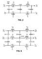
- FIG. 2 illustrates the structure of a switched capacitor block in accordance with an embodiment of the present invention.
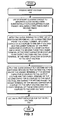
- FIG. 3 presents a flowchart illustrating the voltage-conversion process in accordance with an embodiment of the present invention.
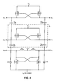
- FIG. 4 illustrates a resonant-clocking circuit in accordance with an embodiment of the present invention.
- FIG. 5 illustrates how voltage converters and a battery can be arranged to implement a power supply in accordance with an embodiment of the present invention.
- FIG. 6 illustrates the structure of a cascadable switched capacitor block (SCB) in accordance with an embodiment of the present invention.
- Embodiments of the present invention provide a technique for arithmetically scaling between a lower voltage, V LO , by a ratio of M:N to a higher voltage, V HI , where M and N are natural numbers.
- V LO lower voltage
- V HI higher voltage
- M and N natural numbers.
- the conversion from input to output is performed with negligible conduction loss, i.e., the ratio of the power out, P o , to power in, P i , can be 99% or higher.
- the only types of electrical components used for energy storage are capacitors and inductors.
- a set of switching devices are used to couple one or more capacitors to each other, the input, or the output during one of two non-overlapping clocking phases. Each switching device provides a very low resistance and low inductance path when on, and an extremely high resistance path when off.
- a resonant-energy circuit is used, which is compatible with the two-phase clocking requirements and the operational characteristics of the switching devices.
- FIG. 1 illustrates a voltage converter in accordance with an embodiment of the present invention.
- an oscillator block 106 receives an oscillator supply voltage V OSC from an oscillator voltage source and produces four versions of the two-phase clock, namely C L , C H , P L and P H .
- This two-phase clock controls two switched capacitor blocks (SCBs) 102 and 104 that drive the output, V HI , during opposite clock phases.
- SCBs 102 and 104 convert a lower input voltage V LO 110 to a higher output voltage V HI 112, which asymptotically equals 2V LO -V B .
- SCB 102 provides an output voltage V HI 112 which equals 2V LO -IR O1 -V B (where R O1 is the effective resistance of SCB 102 and I is the output current), while SCB 104 is decoupled from V HI 112.
- SCB 104 provides an output voltage V HI 112 which equals 2V LO -IR O2 -V B (where R O2 is the effective resistance of SCB 104 and I is the output current), while SCB 102 is decoupled from V HI 112.
- one function of the output capacitor 108 is to supply energy to the output when neither SCB drives the output.
- FIG. 2 illustrates the structure of a switched capacitor block (SCB) 102 in accordance with an embodiment of the present invention.
- SCB 102 includes a capacitor 210 (also referred to as a "pump capacitor") and a set of switching devices 202, 204, 206 and 208.
- switching devices 202, 204, 206 and 208 are power Metal-Oxide-Semiconductor Field-Effect Transistors (MOSFETs).
- MOSFETs Metal-Oxide-Semiconductor Field-Effect Transistors
- FIG. 2 additionally illustrates the connections for MOSFETs 202, 204, 206 and 208. More specifically, MOSFET 202 couples the higher potential terminal of capacitor 210 to V LO 110 under control of clock input C H ; MOSFET 206 couples the lower potential terminal of capacitor 210 to the base voltage, V B 113 under control of clock input C L ; MOSFET 204 couples the higher potential terminal of capacitor 210 to V HI 112 under control of clock input P H ; and MOSFET 208 couples the lower potential terminal of capacitor 210 to V LO 110 under control of clock input P L .
- the higher potential terminal of capacitor 210 is coupled to V LO 110, and the lower potential terminal of capacitor 210 is coupled to V B . This allows the voltage across capacitor 210 to be charged up to V LO - V B .
- capacitor 210 is implemented using a bank of parallel capacitors, wherein each capacitor is a 100 ⁇ F ceramic type capacitor.
- the lower potential terminal of the capacitor bank swings between V B and V LO .
- the gate drive for MOSFET 208 which couples the lower potential terminal of the capacitor bank to V LO , must have a voltage swing of at least V G + V LO , wherein V G is the gate drive voltage required for R ds (on) to reach its minimal on resistance.
- the higher potential terminal of capacitor 210 swings between V LO and V HI .
- MOSFETs 202 and 204 which are connected to the higher potential terminal of the capacitor bank, to swing below V LO .
- These gate drive signals can be biased by the input voltage to swing between V LO + V B + V G and V HI + V B + V G . Note that the energy required to drive each gate is proportional to (V LO +V G ) 2 .
- FIG. 6 illustrates how a voltage higher than V HI may be obtained with the addition of two switching devices and three capacitors. More specifically, FIG. 6 contains all of the circuitry illustrated in FIG. 2 and additionally contains two transistors 602 and 604 and three capacitors 610, 612 and 614. Note that the lower terminal of capacitor 610 attaches to node A 201. During system operation, node A 201 swings from V LO to V HI. Transistor 602 is turned on when node A 201 is at V LO , which causes capacitor 610 to charge up to V HI - V LO . Next, transistor 604 is turned on when node A 201 reaches V HI .
- V XH 612 This causes the output voltage V XH 612 to reach V HI + V LO .
- the circuit illustrated in FIG. 6 effectively acts as a voltage tripler.
- a quadrupler, etc. may be constructed by again applying the transformation from FIG. 2 to FIG. 6 .
- V LO is the input and V B is ground
- V HI provides a 2x output
- V XH provides a 3x output.
- V L provides a 1/2x output
- V XH provides a 3/2x output.
- V XH is the input, V HI provides a 2/3x output and V LO provides a 1/3x output.
- FIG. 3 presents a flowchart illustrating the voltage-conversion process in accordance with an embodiment of the present invention.
- This flow chart covers the operation of the system illustrated in FIG. 1 .
- the system receives an input voltage V LO (step 302).
- the system uses a resonant clocking circuit to generate clock signals with substantially non-overlapping clock phases, including a first phase and a second phase (step 304).
- clock signals are applied to a first set of switching devices (inside SCB 102), so that during the first phase the higher potential terminal of a first capacitor is coupled to the input voltage and the lower potential terminal of the first capacitor is coupled to the base voltage, and during the second phase the higher potential terminal of the first capacitor is coupled to the output voltage and the lower potential terminal of the first capacitor is coupled to the input voltage (step 306).
- clock signals are also applied to a second set of switching devices (inside SCB 104), so that during the first phase the higher potential terminal of the second capacitor is coupled to the output voltage and the lower potential terminal of the second capacitor is coupled to the input voltage, and during the second phase the terminal of the second capacitor is coupled to the input voltage and the lower potential terminal of the second capacitor is coupled to ground (step 308).
- an output capacitor 108 is used to perform a number of functions, including filtering the output voltage (step 310).
- FIG. 4 illustrates a resonant clocking circuit in accordance with an embodiment of the present invention.
- the basic resonant clocking circuit includes two complementary circuit sections that produce opposing clock phases.
- the first circuit section includes inductor 402 and FET 410 and produces output ⁇ 2L .
- the second complementary circuit section includes inductor 404 and FET 408 and produces output ⁇ 1L , wherein ⁇ 1L and ⁇ 2L provide opposing clock phases.
- FETs 408 and 410 are cross-coupled so that the control input for each of FETs 408 and 410 is taken from the output from the complementary circuit section.
- the gate capacitance for each FET is lumped in with the output-load capacitance for the opposing clock phase. (Also note that the load capacitance is the gate capacitance at the SCB.)
- FIG. 4 illustrates corresponding circuitry which generates outputs ⁇ 1H and ⁇ 2H .
- the voltages on outputs ⁇ 1H and ⁇ 2H track the voltages on outputs ⁇ 1L and ⁇ 2L , but are biased to be at higher voltage levels. This is accomplished by using two bootstrap capacitors, C B1 414 and C B2 412, and two cross-coupled FETs 422 and 420 that clamp the elevated clock output to V LO during one phase and then follow the clock output with a positive offset of V LO during the other phase.
- the elevated voltage levels on outputs ⁇ 1H and ⁇ 2H can be used to drive MOSFETs 202 and 204 which are illustrated in FIG. 2 .
- these MOSFETs need gate drive signals that swing between V LO and V HI + V G .
- the dotted line box A can be stacked again to provide the "extra-high" (XH) outputs of FIG. 6 .
- Zener diodes 416 and 418 are coupled between outputs ⁇ 1L and ⁇ 2L , respectively, and ground to protect the circuit against large transient voltages during power up.
- transistors 420 and 422 could be replaced with ordinary diodes with an anode coupled to V LO and a cathode coupled to ⁇ 1H or ⁇ 2H .
- FIG. 5 illustrates how voltage converters and a battery can be arranged to implement a power supply in accordance with an embodiment of the present invention.
- the power supply illustrated in FIG. 5 includes voltage converters 504-508, as well as a number of battery cells 502. Voltage converters 504-508 can be implemented using the voltage converter circuit described above with reference to FIG. 1 .
- battery cells 502 are coupled together in parallel to provide a 1S output for the power supply.
- the 1 S output provides a voltage which is equivalent to a voltage from a single bank of one or more cells coupled together in parallel.
- a 2S output would provide a voltage which is equivalent to a voltage from two banks of cells, wherein the banks are coupled together in series.
- This parallel architecture has a number of advantages, such as eliminating cell imbalance problems, allowing accurate measurements of a cell's state-of-charge, increased design flexibility, and fault tolerance.
- Battery cells 502 also provide an input voltage for voltage converter 504, and the base voltage for voltage converter 504 is tied to ground. Hence, voltage converter 504 doubles this input voltage to provide a 2S output for the power supply.
- the output of voltage converter 504 feeds into the V HI input of voltage converter 505, which divides the 2S output from voltage converter 504 by a factor of two to produce a 1S output for the power supply.
- output of voltage converter 504 feeds into the V LO input of voltage converter 506, and the base voltage for voltage converter 506 is received from the output of battery cells 502.
- voltage converter 506 provides an output which is three times the voltage from battery cells 502. This output provides a 3S output for the power supply.
- circuit illustrated in FIG. 6 also produces a 3S output but uses fewer transistors. More specifically, voltage converters 504 and 506, which are coupled together in FIG. 5 to produce a 3S output, collectively contain 8 transistors. In contrast, the circuit illustrated in FIG. 6 also produces a 3S output, but only contains 6 transistors.
- voltage converter 504 also feeds into the V LO input of voltage converter 507, and the base voltage for voltage converter 507 is tied to ground.
- voltage converter 507 doubles the 2S output from voltage converter 504 to provide an output which is four times the voltage from battery cells 502. This output provides a 4S output for the power supply.
- the 3S output ofvoltage converter 506 also feeds into the V LO input of voltage converter 508, and the base voltage for voltage converter 508 is obtained from the 2S output of voltage converter 504.
- voltage converter 508 adds the 1S difference between the 3S output of voltage converter 506 and the 2S output of voltage converter 504 to the 2S output from voltage converter 504 to provide an output which is four times the voltage from battery cells 502. This output provides a 4S output for the power supply.
- voltage converters 507 and 508 produce the same 4S output but have different requirements for switch and capacitor performance.
- voltage converter 507 performs a direct doubling of the 2S output of voltage converter 504 to produce the 4S output
- voltage converters 506 and 508 are organized in a cascade arrangement to produce the 4S output from the 2S output of voltage converter 504.
- the SCBs 102 and 104 use ceramic capacitors with an ultra-low equivalent series resistance (ESR) and an ultra-low equivalent series inductance (ESL).
- ESR ultra-low equivalent series resistance
- ESL ultra-low equivalent series inductance
- a resonant LC circuit is used in oscillator block 106 to generate gate drive signals for SCBs 102 and 104 without dissipating a significant amount of power. Note that within this resonant LC circuit energy oscillates back and forth between inductive and capacitive circuit elements without a significant resistive or switching loss.
- the switched capacitor blocks (SCBs) 102 and 104 use MOSFETs with a very low on-resistance.
- R O is asymptotically limited by R ON .
- Power dissipation includes conduction losses, I 2 R O , and gate drive losses which are proportional to FC G (V LO + V G ) 2 .
- FC G V LO + V G
- R O decreases with increasing frequency, larger gate capacitance C G , and higher gate-drive voltage, V LO + V G .
- the above-described power-conversion technique is also entirely reversible, which means the technique can also be used to charge the battery cells instead of only discharging the battery cells. Note that the direction of the current and the magnitude of the voltage conversion depends on the relative impedance between V HI and V LO .
Landscapes
- Engineering & Computer Science (AREA)
- Power Engineering (AREA)
- Dc-Dc Converters (AREA)
Abstract
Description
- The disclosed embodiments generally relate to techniques for delivering DC power at different potentials. More specifically, the disclosed embodiments relate to a high-efficiency, switched-capacitor power-conversion technique, which uses a resonant clocking circuit to produce gate drive signals for switching transistors.
- Battery performance is critical to the effective operation of portable computing devices, such as laptop computers. To provide higher supply voltages, battery cells inside portable computing devices are typically stacked in series inside a battery pack. This arrangement provides power efficiently because conduction losses are lower in such a series arrangement. Unfortunately, providing power in this way is inefficient when the power is subsequently down-converted to provide lower voltages for certain system components. For example, the power is usually down-converted using buck converters or other down-conversion techniques that achieve only a 90% efficiency or worse. (Note that power = I·V, whereas conduction loss is proportional to I2R.)
- A battery management unit (BMU) typically controls the charging and discharging processes for a battery pack. However, if the battery cells that comprise the battery pack are not matched in capacity, the battery pack can suffer from an imbalance condition. An imbalanced battery pack has reduced capacity because the cell with the highest state-of charge will cause the charging process to terminate, which means that cells with a lower state-of-charge never get fully charged. Additionally, when the battery pack is discharged, the cell with the least charge may cause the discharging process to stop, even though charge may remain in other cells.
- As an alternative to arranging battery cells in series to achieve higher voltages, voltage converters can be used to increase output voltages. However, existing voltage converter designs suffer from inefficiencies which are a significant power loss.
- Some embodiments of the present invention provide a system that efficiently converts a lower voltage to a higher voltage. This system includes an input which receives the lower voltage, and an output which provides the higher voltage. The system also includes a first capacitor with a higher potential terminal and a lower potential terminal, as well as a first set of switching devices which selectively couple the higher potential and lower potential terminals of the first capacitor between: the lower voltage, the higher voltage, and a voltage which is lower than the lower voltage called the "base voltage." The system additionally includes a resonant clocking circuit which generates clock signals with substantially non-overlapping clock phases, including a first phase and a second phase. This resonant clocking circuit is configured to control the first set of switching devices so that during the first phase, the higher potential terminal of the first capacitor is coupled to the lower voltage and the lower potential terminal of the first capacitor is coupled to the base voltage, and during the second phase, the higher potential terminal of the first capacitor is coupled to the higher voltage and the lower potential terminal of the first capacitor is coupled to the lower voltage.
- In some embodiments, the resonant clocking circuit is an LC oscillator circuit which includes at least one inductance L and at least one capacitance C which is formed at least in part by the gates of one or more switching devices.
- In some embodiments, the system also includes a battery that provides the lower voltage, wherein a lower potential terminal of the battery is coupled to the base voltage and a higher potential terminal of the battery is coupled to the lower voltage.
- In some embodiments, the battery includes multiple battery cells which are coupled in parallel between the input and the base voltage.
- In some embodiments, the system also includes a second set of switching devices and a second capacitor. In these embodiments, the resonant clocking circuit is additionally configured to control the second set of switching devices so that during the first phase, the higher potential terminal of the second capacitor is coupled to the higher voltage and the lower potential terminal of the second capacitor is coupled to the lower voltage, and during the second phase, the higher potential terminal of the second capacitor is coupled to the lower voltage and the lower potential terminal of the second capacitor is coupled to the base voltage.
- In some embodiments, the system also includes an output capacitor coupled between the output and the base voltage. The system can also include an input capacitor coupled between the input and the base voltage.
- In some embodiments, the first set of switching devices includes: a first switch which couples the higher potential terminal of the first capacitor to the lower voltage during the first phase; a second switch which couples the lower potential terminal of the first capacitor to the base voltage during the first phase; a third switch which couples the higher potential terminal of the first capacitor to the higher voltage during the second phase; and a fourth switch which couples the lower potential terminal of the first capacitor to the lower voltage during the second phase.
- In some embodiments, the resonant clocking circuit includes a first phase output and a second phase output. It also includes a first inductor coupled between an oscillator voltage source and the first phase output, and a second inductor coupled between the oscillator voltage source and the second phase output. The resonant clock circuit additionally includes a first transistor with a source terminal coupled to the base voltage or lower, a drain terminal coupled to the first phase output, and a gate terminal coupled to the second phase output, and a second transistor with a source terminal coupled to the base voltage or lower, a drain terminal coupled to the second phase output, and a gate terminal coupled to the first phase output.
- In some embodiments, the first set of switching devices includes power MOSFETs (Metal-Oxide-Semiconductor Field-Effect Transistors).
- In some embodiments, the first capacitor includes one or more ceramic capacitors with an ultra-low equivalent series resistance (ESR) and an ultra-low equivalent series inductance (ESL).
- In some embodiments, the system operates reversibly so that the output becomes the input and vice versa.
-
FIG. 1 illustrates a voltage converter in accordance with an embodiment of the present invention. -
FIG. 2 illustrates the structure of a switched capacitor block in accordance with an embodiment of the present invention. -
FIG. 3 presents a flowchart illustrating the voltage-conversion process in accordance with an embodiment of the present invention. -
FIG. 4 illustrates a resonant-clocking circuit in accordance with an embodiment of the present invention. -
FIG. 5 illustrates how voltage converters and a battery can be arranged to implement a power supply in accordance with an embodiment of the present invention. -
FIG. 6 illustrates the structure of a cascadable switched capacitor block (SCB) in accordance with an embodiment of the present invention. - The following description is presented to enable any person skilled in the art to make and use the invention, and is provided in the context of a particular application and its requirements. Various modifications to the disclosed embodiments will be readily apparent to those skilled in the art, and the general principles defined herein may be applied to other embodiments and applications without departing from the spirit and scope of the present invention. Thus, the present invention is not limited to the embodiments shown, but is to be accorded the widest scope consistent with the principles and features disclosed herein.
- Embodiments of the present invention provide a technique for arithmetically scaling between a lower voltage, VLO, by a ratio of M:N to a higher voltage, VHI, where M and N are natural numbers. By performing the switching at relatively high frequencies, the conversion from input to output is performed with negligible conduction loss, i.e., the ratio of the power out, Po, to power in, Pi, can be 99% or higher. To achieve such high efficiency, the only types of electrical components used for energy storage are capacitors and inductors. Additionally, a set of switching devices are used to couple one or more capacitors to each other, the input, or the output during one of two non-overlapping clocking phases. Each switching device provides a very low resistance and low inductance path when on, and an extremely high resistance path when off.
- As the switching frequency increases, the power required to operate the switches becomes a significant contributor to power dissipation and ultimately limits the efficiency of the system. To overcome this limitation, a resonant-energy circuit is used, which is compatible with the two-phase clocking requirements and the operational characteristics of the switching devices.
-
FIG. 1 illustrates a voltage converter in accordance with an embodiment of the present invention. In the illustrated embodiment, an oscillator block 106 receives an oscillator supply voltage VOSC from an oscillator voltage source and produces four versions of the two-phase clock, namely CL, CH, PL and PH. This two-phase clock controls two switched capacitor blocks (SCBs) 102 and 104 that drive the output, VHI, during opposite clock phases. During forward operation,SCBs input voltage V LO 110 to a higheroutput voltage V HI 112, which asymptotically equals 2VLO-VB. More specifically, during a first clock phase,SCB 102 provides anoutput voltage V HI 112 which equals 2VLO-IRO1-VB (where RO1 is the effective resistance ofSCB 102 and I is the output current), whileSCB 104 is decoupled fromV HI 112. Similarly, during a second clock phase,SCB 104 provides anoutput voltage V HI 112 which equals 2VLO-IRO2-VB (where RO2 is the effective resistance ofSCB 104 and I is the output current), whileSCB 102 is decoupled fromV HI 112. Note that one function of theoutput capacitor 108 is to supply energy to the output when neither SCB drives the output. -
FIG. 2 illustrates the structure of a switched capacitor block (SCB) 102 in accordance with an embodiment of the present invention.SCB 102 includes a capacitor 210 (also referred to as a "pump capacitor") and a set of switchingdevices devices FIG. 2 also depicts the directionality of the body diodes for each of theMOSFETs -
FIG. 2 additionally illustrates the connections forMOSFETs MOSFET 202 couples the higher potential terminal ofcapacitor 210 toV LO 110 under control of clock input CH; MOSFET 206 couples the lower potential terminal ofcapacitor 210 to the base voltage,V B 113 under control of clock input CL;MOSFET 204 couples the higher potential terminal ofcapacitor 210 toV HI 112 under control of clock input PH; and MOSFET 208 couples the lower potential terminal ofcapacitor 210 toV LO 110 under control of clock input PL. - During the first clock phase, the higher potential terminal of
capacitor 210 is coupled toV LO 110, and the lower potential terminal ofcapacitor 210 is coupled to VB. This allows the voltage acrosscapacitor 210 to be charged up to VLO - VB. During the second clock phase, the higher potential terminal ofcapacitor 210 is coupled toV HI 112, and the lower potential terminal ofcapacitor 210 is coupled toV LO 110. In this way, the voltage acrosscapacitor 210 is stacked on top ofV LO 110 to produceoutput voltage V HI 112 = 2VLO-VB-IORO, wherein IO is the output current. - In one embodiment of the present invention,
capacitor 210 is implemented using a bank of parallel capacitors, wherein each capacitor is a 100µF ceramic type capacitor. The lower potential terminal of the capacitor bank swings between VB and VLO. Hence, the gate drive forMOSFET 208, which couples the lower potential terminal of the capacitor bank to VLO, must have a voltage swing of at least VG + VLO, wherein VG is the gate drive voltage required for Rds(on) to reach its minimal on resistance. Likewise, the higher potential terminal ofcapacitor 210 swings between VLO and VHI. Hence, it is not necessary forMOSFETs -
FIG. 6 illustrates how a voltage higher than VHI may be obtained with the addition of two switching devices and three capacitors. More specifically,FIG. 6 contains all of the circuitry illustrated inFIG. 2 and additionally contains twotransistors capacitors capacitor 610 attaches tonode A 201. During system operation,node A 201 swings from VLO to VHI. Transistor 602 is turned on whennode A 201 is at VLO, which causescapacitor 610 to charge up to VHI - VLO. Next,transistor 604 is turned on whennode A 201 reaches VHI. This causes theoutput voltage V XH 612 to reach VHI + VLO. In this way the circuit illustrated inFIG. 6 effectively acts as a voltage tripler. To one skilled in the art, a quadrupler, etc., may be constructed by again applying the transformation fromFIG. 2 to FIG. 6 . Note that because the circuitry illustrated inFIG. 6 is reversible, one can consider any of the points above VB to be the input, and the rest will be outputs. For example, if VLO is the input and VB is ground, VHI provides a 2x output and VXH provides a 3x output. Alternatively, if VHI is the input, VL provides a 1/2x output and VXH provides a 3/2x output. Similarly, if VXH is the input, VHI provides a 2/3x output and VLO provides a 1/3x output. -
FIG. 3 presents a flowchart illustrating the voltage-conversion process in accordance with an embodiment of the present invention. This flow chart covers the operation of the system illustrated inFIG. 1 . During operation, the system receives an input voltage VLO (step 302). Next, the system uses a resonant clocking circuit to generate clock signals with substantially non-overlapping clock phases, including a first phase and a second phase (step 304). - These clock signals are applied to a first set of switching devices (inside SCB 102), so that during the first phase the higher potential terminal of a first capacitor is coupled to the input voltage and the lower potential terminal of the first capacitor is coupled to the base voltage, and during the second phase the higher potential terminal of the first capacitor is coupled to the output voltage and the lower potential terminal of the first capacitor is coupled to the input voltage (step 306).
- These clock signals are also applied to a second set of switching devices (inside SCB 104), so that during the first phase the higher potential terminal of the second capacitor is coupled to the output voltage and the lower potential terminal of the second capacitor is coupled to the input voltage, and during the second phase the terminal of the second capacitor is coupled to the input voltage and the lower potential terminal of the second capacitor is coupled to ground (step 308). Finally, an
output capacitor 108 is used to perform a number of functions, including filtering the output voltage (step 310). -
FIG. 4 illustrates a resonant clocking circuit in accordance with an embodiment of the present invention. Referring to the bottom portion ofFIG. 4 , the basic resonant clocking circuit includes two complementary circuit sections that produce opposing clock phases. The first circuit section includesinductor 402 andFET 410 and produces output ϕ2L. The second complementary circuit section includesinductor 404 andFET 408 and produces output ϕ1L, wherein ϕ1L and ϕ2L provide opposing clock phases. Note thatFETs FETs - During operation of this resonant clocking circuit, energy oscillates back and forth between inductive and capacitive circuit elements without a significant conductive or switching loss. More specifically, in the first circuit section, energy oscillates between
inductor 402 and the load capacitance for output ϕ2L, which is lumped in with the gate capacitance for the opposingFET 408. Similarly, in the second circuit section, energy oscillates betweeninductor 404 and the load capacitance for output ϕ1L, which is lumped in with the gate capacitance for the opposingFET 410. - The top portion of
FIG. 4 illustrates corresponding circuitry which generates outputs ϕ1H and ϕ2H. The voltages on outputs ϕ1H and ϕ2H track the voltages on outputs ϕ1L and ϕ2L, but are biased to be at higher voltage levels. This is accomplished by using two bootstrap capacitors,C B1 414 and CB2 412, and twocross-coupled FETs MOSFETs FIG. 2 . As mentioned in the discussion above, these MOSFETs need gate drive signals that swing between VLO and VHI + VG. As is illustrated in the top portion ofFIG. 4 , the dotted line box A can be stacked again to provide the "extra-high" (XH) outputs ofFIG. 6 . - Note that
Zener diodes 416 and 418 (which, for example, can be 19V Zener diodes) are coupled between outputs ϕ1L and ϕ2L, respectively, and ground to protect the circuit against large transient voltages during power up. Note also thattransistors -
FIG. 5 illustrates how voltage converters and a battery can be arranged to implement a power supply in accordance with an embodiment of the present invention. The power supply illustrated inFIG. 5 includes voltage converters 504-508, as well as a number ofbattery cells 502. Voltage converters 504-508 can be implemented using the voltage converter circuit described above with reference toFIG. 1 . - Note that
battery cells 502 are coupled together in parallel to provide a 1S output for the power supply. (Note that the 1 S output provides a voltage which is equivalent to a voltage from a single bank of one or more cells coupled together in parallel. In contrast, a 2S output would provide a voltage which is equivalent to a voltage from two banks of cells, wherein the banks are coupled together in series.) This parallel architecture has a number of advantages, such as eliminating cell imbalance problems, allowing accurate measurements of a cell's state-of-charge, increased design flexibility, and fault tolerance. -
Battery cells 502 also provide an input voltage forvoltage converter 504, and the base voltage forvoltage converter 504 is tied to ground. Hence,voltage converter 504 doubles this input voltage to provide a 2S output for the power supply. The output ofvoltage converter 504 feeds into the VHI input ofvoltage converter 505, which divides the 2S output fromvoltage converter 504 by a factor of two to produce a 1S output for the power supply. - Additionally, output of
voltage converter 504 feeds into the VLO input ofvoltage converter 506, and the base voltage forvoltage converter 506 is received from the output ofbattery cells 502. As a result,voltage converter 506 provides an output which is three times the voltage frombattery cells 502. This output provides a 3S output for the power supply. - Note that the circuit illustrated in
FIG. 6 also produces a 3S output but uses fewer transistors. More specifically,voltage converters FIG. 5 to produce a 3S output, collectively contain 8 transistors. In contrast, the circuit illustrated inFIG. 6 also produces a 3S output, but only contains 6 transistors. - The output of
voltage converter 504 also feeds into the VLO input ofvoltage converter 507, and the base voltage forvoltage converter 507 is tied to ground. Hence,voltage converter 507 doubles the 2S output fromvoltage converter 504 to provide an output which is four times the voltage frombattery cells 502. This output provides a 4S output for the power supply. - Likewise, the 3S
output ofvoltage converter 506 also feeds into the VLO input ofvoltage converter 508, and the base voltage forvoltage converter 508 is obtained from the 2S output ofvoltage converter 504. Hence,voltage converter 508 adds the 1S difference between the 3S output ofvoltage converter 506 and the 2S output ofvoltage converter 504 to the 2S output fromvoltage converter 504 to provide an output which is four times the voltage frombattery cells 502. This output provides a 4S output for the power supply. Note thatvoltage converters voltage converter 507 performs a direct doubling of the 2S output ofvoltage converter 504 to produce the 4S output, whereasvoltage converters voltage converter 504. - The above-described voltage converter configurations can be extended to provide power supply outputs for any multiple of S. Also, note that any output could be used as an input to charge the battery.
- The above-described power-conversion technique is potentially very efficient. In fact, one implementation achieves a conversion efficiency at many watts of better than 99%. This extremely high conversion efficiency is made possible by a number of factors. (1) Referring to
FIG. 1 , theSCBs SCBs - The above-described power-conversion technique is also entirely reversible, which means the technique can also be used to charge the battery cells instead of only discharging the battery cells. Note that the direction of the current and the magnitude of the voltage conversion depends on the relative impedance between VHI and VLO.
- Also note that we can cascade the bootstrap circuits illustrated in
FIG. 4 and the SCBs illustrated inFIG. 5 to scale the output voltage to higher levels. Alternatively, the output voltage can be scaled using the technique illustrated inFIG. 6 . By scaling the circuits using the above-described techniques, it is possible to produce 3S, 4S, 5S, 6S, and even outputs with larger multiples of S. - The foregoing descriptions of embodiments have been presented for purposes of illustration and description only. They are not intended to be exhaustive or to limit the present description to the forms disclosed. Accordingly, many modifications and variations will be apparent to practitioners skilled in the art. Additionally, the above disclosure is not intended to limit the present description. The scope of the present description is defined by the appended claims.
Claims (13)
- A system for converting between an input voltage and an output voltage, comprising:an input coupled to the input voltage;an output coupled to the output voltage;a first capacitor with a higher potential terminal and a lower potential terminal;a first set of switching devices which selectively couple the higher potential and lower potential terminals of the first capacitor between the input voltage, the output voltage and a base voltage; anda resonant clocking circuit which generates clock signals with substantially non-overlapping clock phases, including a first phase and a second phase, for the first set of switching devices;wherein the resonant clocking circuit is configured to control the first set of switching devices so that during the first phase the higher potential terminal of the first capacitor is coupled to the input voltage and the lower potential terminal of the first capacitor is coupled to the base voltage, and during the second phase the higher potential terminal of the first capacitor is coupled to the output voltage and the lower potential terminal of the first capacitor is coupled to the input voltage.
- The system of claim 1, wherein the resonant clocking circuit is an LC oscillator circuit which includes at least one inductance and at least one capacitance.
- The system of claim 2, wherein the at least one capacitor is a gate of a charge-controlled switching device which is used to implement a switching device in the first set of switching devices.
- The system of claim 1, further comprising a battery that provides the input voltage, wherein a lower potential terminal of the battery is coupled to the base voltage and a higher potential terminal of the battery is coupled to the input, and wherein the battery includes one or more battery cells which are coupled in parallel between the input and the base voltage.
- The system of claim 4, wherein the system comprises a power supply.
- The system of claim 1, further comprising:a second set of switching devices; anda second capacitor with a higher potential terminal and a lower potential terminal;wherein the resonant clocking circuit is configured to control the second set of switching devices so that during the first phase the higher potential terminal of the second capacitor is coupled to the output voltage and the lower potential terminal of the second capacitor is coupled to the input voltage, and during the second phase the higher potential terminal of the second capacitor is coupled to the input voltage and the lower potential terminal of the second capacitor is coupled to the base voltage.
- The system of claim 6, further comprising a capacitor coupled between the output and the input.
- The system of claim 6, further comprising a capacitor coupled between the input and the base voltage.
- The system of claim 6, further comprising a capacitor coupled between the output and the base voltage.
- The system of claim 1, wherein the first set of switching devices includes:a first switch which couples the higher potential terminal of the first capacitor to the input voltage during the first phase;a second switch which couples the lower potential terminal of the first capacitor to the base voltage during the first phase;a third switch which couples the higher potential terminal of the first capacitor to the output voltage during the second phase; anda fourth switch which couples the lower potential terminal of the first capacitor to the input voltage during the second phase.
- The system of claim 2, wherein the resonant clocking circuit is an LC oscillator circuit which includes at least two inductances and at least two capacitances.
- The system of claim 11, wherein the resonant clocking circuit includes:a first phase output;a second phase output;a first inductor coupled between a voltage source and the first phase output;a second inductor coupled between the voltage source and the second phase output;a first transistor with a source terminal coupled to the base voltage, a drain terminal coupled to the first phase output, and a gate terminal coupled to the second phase output; anda second transistor with a source terminal coupled to the base voltage, a drain terminal coupled to the second phase output, and a gate terminal coupled to the first phase output.
- A method for operating the system of claim 12, comprising:receiving an input voltage through an input;using a resonant clocking circuit to generate clock signals with substantially non-overlapping clock phases, including a first phase and a second phase;applying the clock signals to a first set of switching devices which are configured to selectively couple a higher potential terminal and a lower potential terminal of a first capacitor between the input voltage, an output voltage and a base voltage, so that during the first phase the higher potential terminal of the first capacitor is coupled to the input voltage and the lower potential terminal of the first capacitor is coupled to the base voltage or lower, and during the second phase the higher potential terminal of the first capacitor is coupled to an output voltage and the lower potential terminal of the first capacitor is coupled to the input voltage; andproviding the output voltage through an output.
Applications Claiming Priority (1)
| Application Number | Priority Date | Filing Date | Title |
|---|---|---|---|
| US12/535,974 US8320141B2 (en) | 2009-08-05 | 2009-08-05 | High-efficiency, switched-capacitor power conversion using a resonant clocking circuit to produce gate drive signals for switching capacitors |
Publications (1)
| Publication Number | Publication Date |
|---|---|
| EP2306628A1 true EP2306628A1 (en) | 2011-04-06 |
Family
ID=42799547
Family Applications (1)
| Application Number | Title | Priority Date | Filing Date |
|---|---|---|---|
| EP10171642A Withdrawn EP2306628A1 (en) | 2009-08-05 | 2010-08-02 | High-efficiency, switched-capacitor power conversion |
Country Status (7)
| Country | Link |
|---|---|
| US (1) | US8320141B2 (en) |
| EP (1) | EP2306628A1 (en) |
| KR (1) | KR101159989B1 (en) |
| AU (1) | AU2010206040B2 (en) |
| GB (1) | GB2472505B (en) |
| TW (1) | TWI481174B (en) |
| WO (1) | WO2011016948A1 (en) |
Families Citing this family (6)
| Publication number | Priority date | Publication date | Assignee | Title |
|---|---|---|---|---|
| US8933665B2 (en) | 2009-08-05 | 2015-01-13 | Apple Inc. | Balancing voltages between battery banks |
| KR101556838B1 (en) * | 2011-05-05 | 2015-10-13 | 아크틱 샌드 테크놀로지스, 인크. | Dc-dc converter with modular stages |
| WO2013115947A2 (en) * | 2012-01-30 | 2013-08-08 | Apple Inc. | Balancing voltages between battery banks |
| US9679695B2 (en) * | 2012-07-16 | 2017-06-13 | Qualcomm Incorporated | Tuning circuit and method for wireless power transfer systems |
| US9660553B2 (en) * | 2012-11-30 | 2017-05-23 | Ingeteam Power Technology, S.A. | Switching stage, energy conversion circuit, and conversion stage for wind turbines comprising the energy conversion circuit |
| WO2016186142A1 (en) * | 2015-05-19 | 2016-11-24 | デンカ株式会社 | Copolymer for use as polymer blend compatibilizer, and resin composition |
Citations (5)
| Publication number | Priority date | Publication date | Assignee | Title |
|---|---|---|---|---|
| US5051881A (en) * | 1990-07-05 | 1991-09-24 | Motorola, Inc. | Voltage multiplier |
| US5684682A (en) * | 1995-07-19 | 1997-11-04 | Motorola, Inc. | Method and apparatus for selectable DC to DC conversion |
| US20020110009A1 (en) * | 2001-02-07 | 2002-08-15 | Hiroyuki Umeda | DC/DC converter and power supply apparatus for liquid crystal device |
| DE10149938A1 (en) * | 2001-10-10 | 2003-05-08 | Infineon Technologies Ag | Circuit arrangement for contactless chip card has charge pump circuit with amplifier stages with pump nodes, charge reservoir circuit with coupling nodes coupled pump nodes |
| US20040196095A1 (en) * | 2002-07-31 | 2004-10-07 | Nec Corporation | Charge pump-type booster circuit |
Family Cites Families (24)
| Publication number | Priority date | Publication date | Assignee | Title |
|---|---|---|---|---|
| FR2611283B1 (en) * | 1987-02-19 | 1989-06-09 | Em Microelectronic Marin Sa | DEVICE COMPRISING AN ELECTRONIC CIRCUIT FOR PROCESSING AN ANALOG SIGNAL |
| US4807104A (en) * | 1988-04-15 | 1989-02-21 | Motorola, Inc. | Voltage multiplying and inverting charge pump |
| JPH02146955A (en) * | 1988-08-30 | 1990-06-06 | Michiko Naito | Electrostatic transformer |
| US5559478A (en) * | 1995-07-17 | 1996-09-24 | University Of Southern California | Highly efficient, complementary, resonant pulse generation |
| US5760637A (en) * | 1995-12-11 | 1998-06-02 | Sipex Corporation | Programmable charge pump |
| US5677077A (en) * | 1996-02-22 | 1997-10-14 | Compaq Computer Corporation | Sensor circuit for providing maximum and minimum cell voltages of a battery |
| US6188590B1 (en) * | 1996-12-18 | 2001-02-13 | Macronix International Co., Ltd. | Regulator system for charge pump circuits |
| US5920235A (en) * | 1997-06-25 | 1999-07-06 | Northern Telecom Limited | Voltage controlled oscillator integrated circuit |
| GB9716142D0 (en) * | 1997-08-01 | 1997-10-08 | Philips Electronics Nv | Extending battery life in electronic apparatus |
| US6169673B1 (en) * | 1999-01-27 | 2001-01-02 | National Semiconductor Corporation | Switched capacitor circuit having voltage management and method |
| US6385065B1 (en) * | 2000-09-14 | 2002-05-07 | Fairchild Semiconductor Corporation | Low voltage charge pump employing distributed charge boosting |
| US6559689B1 (en) * | 2000-10-02 | 2003-05-06 | Allegro Microsystems, Inc. | Circuit providing a control voltage to a switch and including a capacitor |
| CN1295852C (en) | 2001-02-01 | 2007-01-17 | 皇家菲利浦电子有限公司 | Programmable charge pump device |
| GB2374952A (en) | 2001-04-24 | 2002-10-30 | Ubinetics Ltd | Resonant clock distribution circuit |
| JP3691421B2 (en) * | 2001-09-27 | 2005-09-07 | シャープ株式会社 | Switched capacitor type stabilized power supply circuit |
| US6650163B1 (en) * | 2002-08-08 | 2003-11-18 | International Business Machines Corporation | Clock generator for integrated circuit |
| KR100938292B1 (en) * | 2002-11-28 | 2010-01-21 | 페어차일드코리아반도체 주식회사 | Oscillator Outputs Duty Ratio Differently According to Input Voltage and Has Switching Mode Power Supply |
| EP1665534A1 (en) * | 2003-09-08 | 2006-06-07 | Philips Intellectual Property & Standards GmbH | High frequency control of a semiconductor switch |
| WO2006078244A1 (en) | 2005-01-14 | 2006-07-27 | Semiconductor Components Industries, L.L.C. | Dc-to-dc converter and method therefor |
| TWI277853B (en) * | 2005-03-03 | 2007-04-01 | Novatek Microelectronics Corp | Method for efficiency enhancement in a charge pump circuit and a charge pump control selector |
| US7812579B2 (en) * | 2006-12-30 | 2010-10-12 | Advanced Analogic Technologies, Inc. | High-efficiency DC/DC voltage converter including capacitive switching pre-converter and up inductive switching post-regulator |
| US8040175B2 (en) * | 2007-10-24 | 2011-10-18 | Cypress Semiconductor Corporation | Supply regulated charge pump system |
| WO2009136369A2 (en) | 2008-05-09 | 2009-11-12 | Nxp B.V. | Frequency controlled capacitive power converter |
| JP4613986B2 (en) * | 2008-07-28 | 2011-01-19 | 日本テキサス・インスツルメンツ株式会社 | Switching power supply |
-
2009
- 2009-08-05 US US12/535,974 patent/US8320141B2/en not_active Expired - Fee Related
-
2010
- 2010-07-09 WO PCT/US2010/041557 patent/WO2011016948A1/en not_active Ceased
- 2010-07-15 TW TW099123295A patent/TWI481174B/en not_active IP Right Cessation
- 2010-07-29 AU AU2010206040A patent/AU2010206040B2/en not_active Ceased
- 2010-08-02 EP EP10171642A patent/EP2306628A1/en not_active Withdrawn
- 2010-08-04 KR KR1020100075243A patent/KR101159989B1/en not_active Expired - Fee Related
- 2010-08-04 GB GB1013062A patent/GB2472505B/en not_active Expired - Fee Related
Patent Citations (5)
| Publication number | Priority date | Publication date | Assignee | Title |
|---|---|---|---|---|
| US5051881A (en) * | 1990-07-05 | 1991-09-24 | Motorola, Inc. | Voltage multiplier |
| US5684682A (en) * | 1995-07-19 | 1997-11-04 | Motorola, Inc. | Method and apparatus for selectable DC to DC conversion |
| US20020110009A1 (en) * | 2001-02-07 | 2002-08-15 | Hiroyuki Umeda | DC/DC converter and power supply apparatus for liquid crystal device |
| DE10149938A1 (en) * | 2001-10-10 | 2003-05-08 | Infineon Technologies Ag | Circuit arrangement for contactless chip card has charge pump circuit with amplifier stages with pump nodes, charge reservoir circuit with coupling nodes coupled pump nodes |
| US20040196095A1 (en) * | 2002-07-31 | 2004-10-07 | Nec Corporation | Charge pump-type booster circuit |
Also Published As
| Publication number | Publication date |
|---|---|
| GB201013062D0 (en) | 2010-09-15 |
| KR20110014528A (en) | 2011-02-11 |
| GB2472505A (en) | 2011-02-09 |
| US8320141B2 (en) | 2012-11-27 |
| WO2011016948A1 (en) | 2011-02-10 |
| AU2010206040B2 (en) | 2012-12-20 |
| TWI481174B (en) | 2015-04-11 |
| GB2472505B (en) | 2011-11-23 |
| US20110031956A1 (en) | 2011-02-10 |
| HK1152804A1 (en) | 2012-03-09 |
| CN101997406A (en) | 2011-03-30 |
| KR101159989B1 (en) | 2012-06-26 |
| AU2010206040A1 (en) | 2011-02-24 |
| TW201125273A (en) | 2011-07-16 |
Similar Documents
| Publication | Publication Date | Title |
|---|---|---|
| CN114244105B (en) | Power conversion structure, method including electronic device and chip unit thereof | |
| US9793794B2 (en) | System and method for reducing power loss in switched-capacitor power converters | |
| US11356017B2 (en) | Li-ion-compatible fully-integrated hybrid converter | |
| US10374511B2 (en) | Switched capacitor DC-to-DC converter and power conversion control methods | |
| US9998002B2 (en) | Differential charge pump | |
| US8320141B2 (en) | High-efficiency, switched-capacitor power conversion using a resonant clocking circuit to produce gate drive signals for switching capacitors | |
| US9601932B2 (en) | Balancing voltages between battery banks | |
| Steyaert et al. | When hardware is free, power is expensive! Is integrated power management the solution? | |
| WO2011016974A2 (en) | Controlling power loss in a switched-capacitor power converter | |
| Yang et al. | A 5V input 98.4% peak efficiency reconfigurable capacitive-sigma converter with greater than 90% peak efficiency for the entire 0.4~ 1.2 V output range | |
| CN114552975B (en) | Power conversion system, electronic equipment comprising same and integrated circuit | |
| US11563377B2 (en) | Hybrid power converters | |
| Chen et al. | Dual-path hybrid Dickson converter for high-ratio conversions in point-of-load applications | |
| CN103532382A (en) | Switching power supply circuit | |
| CN110445208B (en) | Charging circuit and terminal | |
| Makharia et al. | Integrating power inductors onto the IC-SOC implementation of inductor multipliers for DC-DC converters | |
| CN116094318A (en) | Current control circuit, electronic equipment and current control method | |
| Maurath et al. | Highly efficient integrated rectifier and voltage boosting circuits for energy harvesting applications | |
| CN216751534U (en) | Chip unit, power supply conversion structure and electronic equipment | |
| CN101997406B (en) | High-efficiency, switched-capacitor power converting system and method | |
| Renz et al. | Motivation and Fundamentals | |
| KR20260023979A (en) | Switch control during multilevel power converter transition systems and methods | |
| Boni et al. | DC–DC converter for fuel-cells and portable devices in digital CMOS technology | |
| Piessens | Tutorial: Charge Pump and Capacitive DCDC Converter Design |
Legal Events
| Date | Code | Title | Description |
|---|---|---|---|
| PUAI | Public reference made under article 153(3) epc to a published international application that has entered the european phase |
Free format text: ORIGINAL CODE: 0009012 |
|
| 17P | Request for examination filed |
Effective date: 20100802 |
|
| AK | Designated contracting states |
Kind code of ref document: A1 Designated state(s): AL AT BE BG CH CY CZ DE DK EE ES FI FR GB GR HR HU IE IS IT LI LT LU LV MC MK MT NL NO PL PT RO SE SI SK SM TR |
|
| AX | Request for extension of the european patent |
Extension state: BA ME RS |
|
| 17Q | First examination report despatched |
Effective date: 20140910 |
|
| STAA | Information on the status of an ep patent application or granted ep patent |
Free format text: STATUS: EXAMINATION IS IN PROGRESS |
|
| STAA | Information on the status of an ep patent application or granted ep patent |
Free format text: STATUS: THE APPLICATION IS DEEMED TO BE WITHDRAWN |
|
| 18D | Application deemed to be withdrawn |
Effective date: 20171103 |