EP2306230A1 - Oeil composé artificiel et son procédé de fabrication - Google Patents
Oeil composé artificiel et son procédé de fabrication Download PDFInfo
- Publication number
- EP2306230A1 EP2306230A1 EP09012409A EP09012409A EP2306230A1 EP 2306230 A1 EP2306230 A1 EP 2306230A1 EP 09012409 A EP09012409 A EP 09012409A EP 09012409 A EP09012409 A EP 09012409A EP 2306230 A1 EP2306230 A1 EP 2306230A1
- Authority
- EP
- European Patent Office
- Prior art keywords
- image sensors
- flexible substrate
- optical channels
- layer
- microlenses
- Prior art date
- Legal status (The legal status is an assumption and is not a legal conclusion. Google has not performed a legal analysis and makes no representation as to the accuracy of the status listed.)
- Granted
Links
- 238000000034 method Methods 0.000 title claims abstract description 52
- 150000001875 compounds Chemical class 0.000 title claims description 68
- 238000004519 manufacturing process Methods 0.000 title description 11
- 230000003287 optical effect Effects 0.000 claims abstract description 105
- 239000000758 substrate Substances 0.000 claims abstract description 83
- 238000003384 imaging method Methods 0.000 claims abstract description 64
- 238000005516 engineering process Methods 0.000 claims description 13
- 239000000463 material Substances 0.000 claims description 9
- 238000007789 sealing Methods 0.000 claims description 7
- 238000005530 etching Methods 0.000 claims description 6
- 238000005520 cutting process Methods 0.000 claims description 4
- 238000004026 adhesive bonding Methods 0.000 claims description 3
- 230000010354 integration Effects 0.000 claims description 3
- 210000000158 ommatidium Anatomy 0.000 description 47
- 108091008695 photoreceptors Proteins 0.000 description 30
- 230000000007 visual effect Effects 0.000 description 23
- 230000004438 eyesight Effects 0.000 description 19
- 238000003491 array Methods 0.000 description 16
- 238000012545 processing Methods 0.000 description 16
- 230000033001 locomotion Effects 0.000 description 15
- HHXNVASVVVNNDG-UHFFFAOYSA-N 1,2,3,4,5-pentachloro-6-(2,3,6-trichlorophenyl)benzene Chemical compound ClC1=CC=C(Cl)C(C=2C(=C(Cl)C(Cl)=C(Cl)C=2Cl)Cl)=C1Cl HHXNVASVVVNNDG-UHFFFAOYSA-N 0.000 description 14
- 238000013459 approach Methods 0.000 description 14
- 235000012431 wafers Nutrition 0.000 description 12
- 241000238631 Hexapoda Species 0.000 description 11
- 238000013461 design Methods 0.000 description 11
- XUIMIQQOPSSXEZ-UHFFFAOYSA-N Silicon Chemical compound [Si] XUIMIQQOPSSXEZ-UHFFFAOYSA-N 0.000 description 9
- 229910052710 silicon Inorganic materials 0.000 description 9
- 239000010703 silicon Substances 0.000 description 9
- 230000005693 optoelectronics Effects 0.000 description 7
- 230000008569 process Effects 0.000 description 7
- 238000000926 separation method Methods 0.000 description 6
- 230000035945 sensitivity Effects 0.000 description 5
- 230000003044 adaptive effect Effects 0.000 description 4
- 230000004075 alteration Effects 0.000 description 4
- 238000005452 bending Methods 0.000 description 4
- 230000006378 damage Effects 0.000 description 4
- 239000004205 dimethyl polysiloxane Substances 0.000 description 4
- 229920000435 poly(dimethylsiloxane) Polymers 0.000 description 4
- 229910001285 shape-memory alloy Inorganic materials 0.000 description 4
- 241000251539 Vertebrata <Metazoa> Species 0.000 description 3
- 238000004458 analytical method Methods 0.000 description 3
- 210000001507 arthropod compound eye Anatomy 0.000 description 3
- 230000008901 benefit Effects 0.000 description 3
- 210000004556 brain Anatomy 0.000 description 3
- 230000008859 change Effects 0.000 description 3
- 238000001514 detection method Methods 0.000 description 3
- 210000003128 head Anatomy 0.000 description 3
- 229920000642 polymer Polymers 0.000 description 3
- 241000156978 Erebia Species 0.000 description 2
- 241001465754 Metazoa Species 0.000 description 2
- 238000004891 communication Methods 0.000 description 2
- 238000012937 correction Methods 0.000 description 2
- 230000000694 effects Effects 0.000 description 2
- 238000005538 encapsulation Methods 0.000 description 2
- 238000000605 extraction Methods 0.000 description 2
- 239000000835 fiber Substances 0.000 description 2
- 239000011521 glass Substances 0.000 description 2
- 239000003292 glue Substances 0.000 description 2
- 239000012528 membrane Substances 0.000 description 2
- -1 polydimethylsiloxane Polymers 0.000 description 2
- 230000010076 replication Effects 0.000 description 2
- 238000005070 sampling Methods 0.000 description 2
- 238000012216 screening Methods 0.000 description 2
- 239000004065 semiconductor Substances 0.000 description 2
- 229910000679 solder Inorganic materials 0.000 description 2
- 125000006850 spacer group Chemical group 0.000 description 2
- 238000001228 spectrum Methods 0.000 description 2
- 230000007480 spreading Effects 0.000 description 2
- 238000003892 spreading Methods 0.000 description 2
- 230000006641 stabilisation Effects 0.000 description 2
- 238000011105 stabilization Methods 0.000 description 2
- 241000256837 Apidae Species 0.000 description 1
- 241000256844 Apis mellifera Species 0.000 description 1
- 206010034960 Photophobia Diseases 0.000 description 1
- 208000027418 Wounds and injury Diseases 0.000 description 1
- 230000032683 aging Effects 0.000 description 1
- 230000003190 augmentative effect Effects 0.000 description 1
- 230000006399 behavior Effects 0.000 description 1
- 238000012512 characterization method Methods 0.000 description 1
- 230000000295 complement effect Effects 0.000 description 1
- 230000006835 compression Effects 0.000 description 1
- 238000007906 compression Methods 0.000 description 1
- 238000010276 construction Methods 0.000 description 1
- 230000008878 coupling Effects 0.000 description 1
- 238000010168 coupling process Methods 0.000 description 1
- 238000005859 coupling reaction Methods 0.000 description 1
- 230000007423 decrease Effects 0.000 description 1
- 230000001419 dependent effect Effects 0.000 description 1
- 238000011161 development Methods 0.000 description 1
- 230000018109 developmental process Effects 0.000 description 1
- 238000006073 displacement reaction Methods 0.000 description 1
- 238000009429 electrical wiring Methods 0.000 description 1
- 238000005265 energy consumption Methods 0.000 description 1
- 230000005669 field effect Effects 0.000 description 1
- 238000005111 flow chemistry technique Methods 0.000 description 1
- 230000008014 freezing Effects 0.000 description 1
- 238000007710 freezing Methods 0.000 description 1
- PCHJSUWPFVWCPO-UHFFFAOYSA-N gold Chemical compound [Au] PCHJSUWPFVWCPO-UHFFFAOYSA-N 0.000 description 1
- 239000010931 gold Substances 0.000 description 1
- 229910052737 gold Inorganic materials 0.000 description 1
- 238000010191 image analysis Methods 0.000 description 1
- 230000006872 improvement Effects 0.000 description 1
- 208000014674 injury Diseases 0.000 description 1
- 238000005304 joining Methods 0.000 description 1
- 238000003698 laser cutting Methods 0.000 description 1
- 208000013469 light sensitivity Diseases 0.000 description 1
- 239000011159 matrix material Substances 0.000 description 1
- 238000005259 measurement Methods 0.000 description 1
- 229910044991 metal oxide Inorganic materials 0.000 description 1
- 150000004706 metal oxides Chemical class 0.000 description 1
- 210000003205 muscle Anatomy 0.000 description 1
- 229930014626 natural product Natural products 0.000 description 1
- 210000004179 neuropil Anatomy 0.000 description 1
- 238000004806 packaging method and process Methods 0.000 description 1
- 238000000059 patterning Methods 0.000 description 1
- 238000000206 photolithography Methods 0.000 description 1
- 230000016732 phototransduction Effects 0.000 description 1
- 239000000049 pigment Substances 0.000 description 1
- 150000003071 polychlorinated biphenyls Chemical class 0.000 description 1
- 229920000307 polymer substrate Polymers 0.000 description 1
- 238000007781 pre-processing Methods 0.000 description 1
- 238000007639 printing Methods 0.000 description 1
- 108020003175 receptors Proteins 0.000 description 1
- 238000011084 recovery Methods 0.000 description 1
- 230000009467 reduction Effects 0.000 description 1
- 238000009877 rendering Methods 0.000 description 1
- 230000003362 replicative effect Effects 0.000 description 1
- 238000011160 research Methods 0.000 description 1
- 230000004044 response Effects 0.000 description 1
- 230000000284 resting effect Effects 0.000 description 1
- 210000001525 retina Anatomy 0.000 description 1
- 238000012552 review Methods 0.000 description 1
- 238000009958 sewing Methods 0.000 description 1
- 230000035882 stress Effects 0.000 description 1
- 230000001629 suppression Effects 0.000 description 1
- 230000004083 survival effect Effects 0.000 description 1
- 230000002123 temporal effect Effects 0.000 description 1
- 238000012546 transfer Methods 0.000 description 1
- 238000010200 validation analysis Methods 0.000 description 1
- 230000004304 visual acuity Effects 0.000 description 1
- 239000002699 waste material Substances 0.000 description 1
- XLYOFNOQVPJJNP-UHFFFAOYSA-N water Substances O XLYOFNOQVPJJNP-UHFFFAOYSA-N 0.000 description 1
Images


Classifications
-
- G—PHYSICS
- G02—OPTICS
- G02B—OPTICAL ELEMENTS, SYSTEMS OR APPARATUS
- G02B13/00—Optical objectives specially designed for the purposes specified below
- G02B13/06—Panoramic objectives; So-called "sky lenses" including panoramic objectives having reflecting surfaces
-
- G—PHYSICS
- G02—OPTICS
- G02B—OPTICAL ELEMENTS, SYSTEMS OR APPARATUS
- G02B13/00—Optical objectives specially designed for the purposes specified below
- G02B13/001—Miniaturised objectives for electronic devices, e.g. portable telephones, webcams, PDAs, small digital cameras
-
- G—PHYSICS
- G02—OPTICS
- G02B—OPTICAL ELEMENTS, SYSTEMS OR APPARATUS
- G02B3/00—Simple or compound lenses
- G02B3/0006—Arrays
- G02B3/0012—Arrays characterised by the manufacturing method
- G02B3/0025—Machining, e.g. grinding, polishing, diamond turning, manufacturing of mould parts
-
- H—ELECTRICITY
- H04—ELECTRIC COMMUNICATION TECHNIQUE
- H04N—PICTORIAL COMMUNICATION, e.g. TELEVISION
- H04N25/00—Circuitry of solid-state image sensors [SSIS]; Control thereof
- H04N25/40—Extracting pixel data from image sensors by controlling scanning circuits, e.g. by modifying the number of pixels sampled or to be sampled
- H04N25/41—Extracting pixel data from a plurality of image sensors simultaneously picking up an image, e.g. for increasing the field of view by combining the outputs of a plurality of sensors
-
- H—ELECTRICITY
- H10—SEMICONDUCTOR DEVICES; ELECTRIC SOLID-STATE DEVICES NOT OTHERWISE PROVIDED FOR
- H10K—ORGANIC ELECTRIC SOLID-STATE DEVICES
- H10K39/00—Integrated devices, or assemblies of multiple devices, comprising at least one organic radiation-sensitive element covered by group H10K30/00
- H10K39/30—Devices controlled by radiation
- H10K39/32—Organic image sensors
-
- H—ELECTRICITY
- H01—ELECTRIC ELEMENTS
- H01L—SEMICONDUCTOR DEVICES NOT COVERED BY CLASS H10
- H01L2224/00—Indexing scheme for arrangements for connecting or disconnecting semiconductor or solid-state bodies and methods related thereto as covered by H01L24/00
- H01L2224/01—Means for bonding being attached to, or being formed on, the surface to be connected, e.g. chip-to-package, die-attach, "first-level" interconnects; Manufacturing methods related thereto
- H01L2224/02—Bonding areas; Manufacturing methods related thereto
- H01L2224/04—Structure, shape, material or disposition of the bonding areas prior to the connecting process
- H01L2224/05—Structure, shape, material or disposition of the bonding areas prior to the connecting process of an individual bonding area
- H01L2224/0554—External layer
- H01L2224/0555—Shape
- H01L2224/05552—Shape in top view
- H01L2224/05554—Shape in top view being square
-
- H—ELECTRICITY
- H01—ELECTRIC ELEMENTS
- H01L—SEMICONDUCTOR DEVICES NOT COVERED BY CLASS H10
- H01L2224/00—Indexing scheme for arrangements for connecting or disconnecting semiconductor or solid-state bodies and methods related thereto as covered by H01L24/00
- H01L2224/01—Means for bonding being attached to, or being formed on, the surface to be connected, e.g. chip-to-package, die-attach, "first-level" interconnects; Manufacturing methods related thereto
- H01L2224/42—Wire connectors; Manufacturing methods related thereto
- H01L2224/47—Structure, shape, material or disposition of the wire connectors after the connecting process
- H01L2224/48—Structure, shape, material or disposition of the wire connectors after the connecting process of an individual wire connector
- H01L2224/4805—Shape
- H01L2224/4809—Loop shape
- H01L2224/48091—Arched
-
- H—ELECTRICITY
- H01—ELECTRIC ELEMENTS
- H01L—SEMICONDUCTOR DEVICES NOT COVERED BY CLASS H10
- H01L2224/00—Indexing scheme for arrangements for connecting or disconnecting semiconductor or solid-state bodies and methods related thereto as covered by H01L24/00
- H01L2224/01—Means for bonding being attached to, or being formed on, the surface to be connected, e.g. chip-to-package, die-attach, "first-level" interconnects; Manufacturing methods related thereto
- H01L2224/42—Wire connectors; Manufacturing methods related thereto
- H01L2224/47—Structure, shape, material or disposition of the wire connectors after the connecting process
- H01L2224/49—Structure, shape, material or disposition of the wire connectors after the connecting process of a plurality of wire connectors
- H01L2224/491—Disposition
- H01L2224/4912—Layout
- H01L2224/49175—Parallel arrangements
-
- H—ELECTRICITY
- H01—ELECTRIC ELEMENTS
- H01L—SEMICONDUCTOR DEVICES NOT COVERED BY CLASS H10
- H01L27/00—Devices consisting of a plurality of semiconductor or other solid-state components formed in or on a common substrate
- H01L27/14—Devices consisting of a plurality of semiconductor or other solid-state components formed in or on a common substrate including semiconductor components sensitive to infrared radiation, light, electromagnetic radiation of shorter wavelength or corpuscular radiation and specially adapted either for the conversion of the energy of such radiation into electrical energy or for the control of electrical energy by such radiation
- H01L27/144—Devices controlled by radiation
- H01L27/146—Imager structures
- H01L27/14601—Structural or functional details thereof
- H01L27/14603—Special geometry or disposition of pixel-elements, address-lines or gate-electrodes
-
- H—ELECTRICITY
- H01—ELECTRIC ELEMENTS
- H01L—SEMICONDUCTOR DEVICES NOT COVERED BY CLASS H10
- H01L27/00—Devices consisting of a plurality of semiconductor or other solid-state components formed in or on a common substrate
- H01L27/14—Devices consisting of a plurality of semiconductor or other solid-state components formed in or on a common substrate including semiconductor components sensitive to infrared radiation, light, electromagnetic radiation of shorter wavelength or corpuscular radiation and specially adapted either for the conversion of the energy of such radiation into electrical energy or for the control of electrical energy by such radiation
- H01L27/144—Devices controlled by radiation
- H01L27/146—Imager structures
- H01L27/14601—Structural or functional details thereof
- H01L27/14625—Optical elements or arrangements associated with the device
- H01L27/14627—Microlenses
-
- H—ELECTRICITY
- H01—ELECTRIC ELEMENTS
- H01L—SEMICONDUCTOR DEVICES NOT COVERED BY CLASS H10
- H01L27/00—Devices consisting of a plurality of semiconductor or other solid-state components formed in or on a common substrate
- H01L27/14—Devices consisting of a plurality of semiconductor or other solid-state components formed in or on a common substrate including semiconductor components sensitive to infrared radiation, light, electromagnetic radiation of shorter wavelength or corpuscular radiation and specially adapted either for the conversion of the energy of such radiation into electrical energy or for the control of electrical energy by such radiation
- H01L27/144—Devices controlled by radiation
- H01L27/146—Imager structures
- H01L27/14601—Structural or functional details thereof
- H01L27/14636—Interconnect structures
Definitions
- the present invention relates to an imaging system which may be used as an artificial compound eye and a method for fabrication thereof.
- the vertebrate eye ( Fig. 10 , left) has provided inspiration for the design of conventional cameras, which consist of a planar image sensor in the focal plane of single-aperture optics (single or multiple co-axial lenses). Their purpose is to provide a faithful rendering of the visual world that can be processed by image analysis algorithms for a large variety of purposes, especially for object recognition.
- image analysis algorithms for a large variety of purposes, especially for object recognition.
- vision systems require complex and fast computation in order to extract motion-related information from a sequence of high-resolution images.
- the insect compound eye ( Fig. 10 , centre and right), instead, consists of a curved array of microlenses, each conveying photons to a separate set of one or more photoreceptors.
- compound eye design offers a comparatively lower resolution than the vertebrate eye, it is very efficient for local and global motion analysis over a large field-of-view (FOV), making it an excellent sensor for accurate and fast navigation in 3D dynamic environments.
- compound eyes take several shapes and curvatures to fit the head and viewing directions of very different types of insects while offering the same functionality.
- Miniaturized cameras are important features for next-generation customer products.
- Digital micro-cameras which are based on miniaturized classical lens designs, are rarely smaller than 4 x 4 x 3 mm 3 for a VGA (Video Graphics Array) with approximately 60° field-of view.
- CMOS Complementary Metal Oxide Semiconductor
- the thickness of conventional imaging optics is typically in the same order of magnitude as is their focal length.
- the digital sensor diagonal and the given field-of-view determine the required magnification of the lens. For a conventional lens this magnification is defined by its focal length, while for compound eyes it is not.
- the Argus Eye uses a network of cameras, with each of them occupying a different part of the visual sphere.
- the underlying calibration and visual processing of the Argus Eye system is straightforward, it needs high-resolution cameras for the accurate recovery of motion information and hence has a high computational demand.
- Insect compound eyes display high temporal resolution, small volumes, and large fields of view at the cost of comparatively low angular resolution (see Land, M. (1997) Visual Acuity in Insects. Annual Review of Entomology, 42, 147-177 ).
- small invertebrates such as flies or honeybees
- the compound eyes are a perfect solution for quickly obtaining visual information about the environment without overloading their brain with complex image processing.
- a biological apposition compound eye consists of an array of microlenses on a curved surface. Each microlens is associated with a small group of photoreceptors in its focal plane.
- Apposition compound eyes have mainly evolved in diurnal insects such as flies ( Horridge, G., A.
- a single microlens-photoreceptor unit forms one optical channel and is commonly referred to as ommatidium ( Kirschfeld, K. (1974) The absolute sensitivity of lens and compound eyes. Z. Naturforsch., 29 pp. 592-596 ; see also Fig. 10 , right).
- Gradient refractive index cones and pigments which form opaque walls between adjacent ommatidia, prevent light from being focused by a channel's microlens onto an adjacent channel's receptor ("crosstalk").
- Natural apposition compound eyes contain from several hundreds (water fly) to tens of thousands (honeybee or Japanese dragon fly) of these ommatidia packed in non-uniform hexagonal arrays ( Land, M., and Nilsson, D.-E. (2002) Animal Eyes. Oxford animal biology series, Oxford University Press ).
- planar compound eye had a restricted field-of-view of about 65°, which is by far less than that of natural compound eyes, which allow almost spherical vision.
- PNAS 105 48 (48) pp. 18675-18680 ).
- a key aspect of this device is the flexible wiring between adjacent silicon photoreceptors arranged on a lattice, which allows compression of the lattice.
- the resulting concave silicon optoelectronics is coupled with a single lens, just as in human eyes, and thus sidesteps the alignment and crosstalk problems that would arise when hypothetically coupled to a curved array of microlenses to realize a curved artificial compound eye.
- the object is solved by a method for fabricating an imaging system according to claim 1 and a mechanically flexible imaging system according to claim 17.
- the technological key to functional and usable curved artificial eyes is a highly accurate alignment of microlenses and photoreceptors to an array of optical channels or ommatidia and the positional and rotational correlation within the array on a common flexible substrate. It is the finding of the present invention that the highly accurate alignment can be achieved when the integration of an optics layer (microlenses) with an optoelectronics layer (photoreceptors) and with a flexible layer is performed in the planar stage and the curvature is introduced at a later stage, when the correlation between the three layers of each ommatidium is fixed.
- Embodiments of the present invention provide a method for fabricating an imaging system, the method comprising providing a flexible substrate, providing a first layer comprising a plurality of microlenses and providing a second layer comprising a plurality of image sensors.
- the first and the second layer are stacked onto the flexible substrate by attaching the plurality of image sensors to the flexible substrate, such that each of the plurality of microlenses and image sensors are aligned to form a plurality of optical channels, each optical channel comprising at least one microlens and an associated image sensor.
- the optical channels are mechanically separated such that the separated optical channels remain attached to the flexible substrate to form a mechanically flexible imaging system.
- stacking the plurality of microlenses onto the plurality of image sensors is performed before attaching the plurality of image sensors to the flexible substrate.
- the first and second layer are provided as planar layers, respectively, and stacking the first layer onto the second layer, attaching the stacked first and second layer onto the flexible substrate and mechanically separating the optical channels all occur in a planar state.
- mechanically separating the optical channels may comprise cutting, sawing or etching the stacked first and second layer to physically separate neighbouring optical channels.
- an imaging system which may serve as a basis for an artificial compound eye, may be obtained by fabricating individual image sensors, e. g., photodiode-pixels, or small groups thereof on an image sensor wafer. Also, corresponding microlens or aperture arrays are fabricated on a microlens or aperture wafer, which may be stacked onto the image sensor wafer by bonding the two together. The resulting wafer stack may be attached to a flexible substrate, which may be a flexible printed circuit board (PCB), e.g. a dicing tape. After attaching the stacked wafers to the flexible substrate, the optical channels or ommatidia (“camera-cubes”) are separated by dicing but leaving them on the flexible substrate.
- PCB flexible printed circuit board
- a portion of the flexible substrate which shall form the artificial compound eye may be cut out.
- the obtained flexible imaging system may then be bonded to a convex basis with a desired radius of curvature such that a resulting inter-ommaditial angle is well matched to an acceptance angle of optical individual channels or, in the case of using several image sensors or pixels per microlens, such that the channel is matched to the sampling angle as well.
- the image sensors or pixels are electrically connected to read-out electronics for further data processing.
- the flexible substrate may be a flexible PCB (e.g. a dicing tape) wiring out electrical connections of the image sensors or photoreceptors. Electrical connections from the image sensors to the flexible PCB can either be obtained by wire-bonding the image sensors down to electrical interconnections in the flexible PCB, or by connecting the image sensors via "through silicon interconnects" (TSI, e.g. VIAS) at the backsides of the image sensors.
- TSI through silicon interconnects
- a mechanically flexible imaging system comprising a flexible substrate having attached thereto a plurality of image sensors carrying a plurality of microlenses to form a plurality of optical channels, each optical channel comprising at least one microlens and at least one associated image sensor, and wherein at least some of the optical channels are mechanically separated to form the mechanically flexible imaging system.
- Embodiments of the present invention enable the design, prototyping, programming and validation of fully functional artificial compound eyes, which are composed of microlens arrays integrated with adaptive image sensors or photoreceptors, e.g., made of analog verylarge-scale-integration circuits (aVLSI), on flexible electronic substrates.
- the output of the artificial compound eyes may be processed by vision filters implemented in encapsulated programmable devices, such as micro-controllers or field programmable gate arrays (FPGA) for fast extraction of motion-related information.
- embodiments of the present invention may offer much larger field-of-view, nearly infinite depth-of-field (no focusing needed), higher sensitivity, no image blurring and off-axis aberrations, because the distance between the optical surface and the photoreceptors will be constant over the entire field-of view, and because each optical channel will work under perpendicular light incidence for its individual viewing direction.
- imaging systems according to embodiments of the present invention allow the use of different focal length for the same field-of-view.
- the curved shape of the resulting artificial compound eyes may offer space within the convexity for embedding processing units, battery, wireless communication, and inertial sensors, such as accelerometers and rate gyroscopes, which may be used for motion-related computation.
- inertial sensors such as accelerometers and rate gyroscopes, which may be used for motion-related computation.
- these components must be packed separately because the space between the convex lens and the planar image sensor must be transparent.
- Fig. 1 shows a high-level flow chart of a method 100 for fabricating an imaging system according to an embodiment of the present invention.
- a flexible substrate In a preliminary fabrication step 110, a flexible substrate, a first layer comprising a plurality of microlenses and a second layer comprising a plurality of image sensors or photoreceptors are provided.
- the first and the second layer are stacked onto the flexible substrate by attaching the plurality of image sensors to the flexible substrate, such that each of the plurality of microlenses and image sensors are aligned to form a plurality of optical channels (ommatidia), wherein each optical channel (ommatidium) comprises at least one microlens and at least one associated image sensor.
- the optical channels are mechanically separated 130 such that the separated optical channels remain attached to the flexible substrate to form a mechanically flexible imaging system.
- stacking the plurality of microlenses onto the plurality of image sensors is performed before attaching the plurality of image sensors to the flexible substrate.
- the first and second layer are provided as planar layers, respectively, and stacking the first layer onto the second layer, attaching 120 the stacked first and second layer onto the flexible substrate and mechanically separating 130 the optical channels all occur in a planar state.
- mechanically separating 130 the optical channels may comprise cutting, sawing or etching the stacked first and second layer to physically separate neighboring optical channels.
- the provided flexible substrate may be a flexible printed circuit board (e.g. a dicing tape) as ductile mechanical support for the optical channels.
- a flexible printed circuit board e.g. a dicing tape
- electrical connections for the plurality of image sensors to associated readout electronics via the flexible PCB are provided.
- Flexible in the present context means a capability of being bent or flexed without injury or damage.
- An example of a flexible substrate is shown in Fig. 2a .
- the flexible substrate 200 shown in Fig. 2a is an example of a one-dimensional flexible PCB with included electronics 202.
- Fig. 2a (top) shows a backside of the flexible PCB 200 with wiring 204.
- the bottom image shows a sensing side of the flexible PCB 200 with indicated placement 210 of 16 one-dimensionally arranged image sensors.
- the flexible PCB 200 acts as mechanical support for the artificial ommatidia and as electrical connectivity to readout electronics.
- the flexible PCB 200 may be very thin, e.g. down to 100 microns, with 50-100 micron wide electrical lines 204, which may act as connective pads for a wire bonding process.
- the flexible substrate may also be a ductile or bendable tape, in particular a dicing tape for the (normally temporary) fixing of wafers.
- the step 110 of providing the first layer with the plurality of microlenses comprises providing a wafer 220 carrying a microlens-array 230 comprising the plurality of microlenses 232, which is exemplarily shown in Fig. 2b .
- the first layer 220 carrying the plurality of microlenses 232 may be designed and/or fabricated by lithographic methods on wafer-scale to achieve a thickness d in the order of 100 microns.
- Parameters such as geometry of the components, number of ommatidia per patch, optical properties of each ommatidium (field-of-view, resolution, sensitivity, overall size constraints), architecture of the underlying vision chip (photoreceptor size and layout, electrical circuitry to be built-in bonding pads), and the way the photoreceptors are electrically interconnected, may serve as input for the layout of the microlens array 230 and underlying aperture arrays (not shown) for suppression of optical channel crosstalk.
- the first layer 220 carrying the plurality of microlenses 232 may be a wafer comprising a glass or polymer substrate for the microlenses 232.
- the first layer 220 may be combined with aperture arrays and polymer spacer layers to micro-optic sandwiches of e.g. glass substrates, aperture arrays and polymer spacer layers.
- Fig. 2c shows a schematic side-view of the second layer 240 comprising the plurality of image sensors or photoreceptors 242.
- the second layer 240 may be fitted underneath the first layer 220 carrying the microlens array 230.
- vision chips comprising the image sensors 242 cannot be conventional imagers for several reasons. First, they need to provide space around each photoreceptor 242 for the separation step 130 that will occur once the first layer 220 carrying the microlens array 230 has been bonded, e.g. by gluing, on top of the image sensor wafer 240.
- the fact that each photoreceptor 242 may be singulated also means that each of them may need connecting pads for wire bonding to the underlying flexible substrate 200 or directly to neighboring optical channels.
- passive circuitry 244 e.g. front end electronics like a read-out electronic, may be added next to each photoreceptor 242.
- External bond pads 246 serve for connecting the second layer 240, i.e. the optoelectronic photoreceptors 242, to further (e.g. back end) read-out circuitry (not shown).
- the image sensor chips may extend beyond at least a part of the periphery of the optic to allow access to the bond pads on the image censor chip also after having applied the optic to the image sensor chip.
- a VLSI technology may be used to provide very low-power image sensor circuits by relying on sub-threshold methods (see Liu, S., Kramer, J., Indiveri, G., Delbschreib, T., and Douglas, R. (2003) Analog VLSI: Circuits and Principles. MIT Press, Cambridge, MA ).
- additional functionalities include the enhancement of the dynamic range by using a self-adaptive circuit (see Delbschreib, T., Mead, C. (1995) Analog VLSI phototransduction by continuous-time, adaptive, logarithmic photoreceptor circuits. IEEE Computer Society Press, pp.
- Such an adaptive photoreceptor 242 is interesting not only for DC operation, but also for AC operations because it is designed in such a way that a sudden change in light level is transformed into an impulse that gets back to the initial resting level with a time constant that depends on the light change amplitude.
- Figs. 3a-e show a method for fabricating the flexible imaging system according to an embodiment of the present invention.
- a stacking of the plurality of microlenses 220 onto the plurality of image sensors 240 is performed before attaching the second layer 240 comprising the plurality of image sensors 242 to the flexible substrate 200 (see Fig. 3d ).
- the first and the second layers 220, 240 are stacked onto each other such that each of the plurality of microlenses 232 and image sensors 242 are aligned to form a plurality of optical channels 300, wherein each optical channel 300 comprises at least one microlens 232 and at least one associated image sensor 242.
- each optical channel 300 comprises at least one microlens 232 and at least one associated image sensor 242.
- the mechanical separation of the optical channels 300 may comprise cutting, sawing, etching, dicing, or laser dicing the stacked first and second layers 220, 240 to physically separate neighboring optical channels 300.
- the flexible substrate 200 is not cut or mechanically separated, because it acts as mechanical support for the optical channels 300.
- Figs. 3f-k show a method for fabricating the flexible imaging system according to another embodiment of the present invention.
- the first and the second layers 220, 240 shown in Figs. 3f and 3g correspond substantially to those of Figs. 3a and 3b , except that in the image sensor layer 240 the front end electronics (e.g. read-out electronics) are integrated such that each image sensor has associated therewith a front-end electronic circuit 244.
- the first and the second layers 220, 240 shown in Figs. 3f and 3g are combined (see Fig. 3h ) and attached onto the mechanically flexible substrate 200. While Figs. 3f-h show side views of the first and the second layers 220, 240, Figs.
- FIG. 3i-j show top views of the separated layers.
- Fig. 3i shows the arrangement of a single image sensor 242 per column while
- Fig. 3j shows an embodiment comprising a plurality of image sensors 242 per column.
- the front-end electronics 242 are arranged at the extremity of the layer and the pads 246 are arranged in the respective column, i.e. along a direction perpendicular to the bending direction.
- Fig. 3k is again a side view showing the mechanically flexible imaging system having the optical channels 300 which are mechanically separated in a manner as described above.
- the front-end electronics and the bond pads are integrated and placed at the extremity of each column, so that other than in the embodiments shown in Figs. 2c and 3a-e there is no need to arrange the readout electronics and pads at the periphery of the layer 240.
- the read-out electronics and pads are simply integrated and arranged at the tip of each photosensor array or each column of ommatidia. There is no need to place the electronics at a back side but just near the pixels of each columns' extremity. This arrangement is advantageous as it avoids the wire-bonding between each column so that bending the flexible substrate will not damage the wire connections.
- a precise combination of microlens- and photoreceptor arrays onto the mechanically flexible substrate 200 including electrical wiring and encapsulation may be achieved due to the fact that all assembly steps occur in a planar state, which allows high precision, while the final optical channel or ommatidia patch will be completely mechanically flexible.
- providing the first and second layer 220, 240 comprises providing planar layers, respectively, wherein stacking the first layer 220 onto the second layer 240, attaching the stacked first and second layer onto the flexible substrate 200)and mechanically separating the optical channels 300 occur in a planar state.
- a matching of alignment marks in both structures may be used.
- a sub-micron precise lateral and rotational alignment of the image sensors 242 with respect to their corresponding microlenses 232 is possible.
- chip bonding extremely short focal lengths of the microlenses 232 has to be dealt with.
- An axial or vertical distance between the optics layer 220 and the image sensors 242 of the ommatidia 300 could be determined by the amount and viscosity of an applied UV-glue and/or by active setting via manipulation stages.
- the optical channels 300 or columns thereof may be singulated from each other by wafer dicing only once the interconnection between the lenslets 232 and the vision chip 240 is permanently fixed and the lens-vision-chip-sandwich has been applied to the flexible PCB 200, which at the same time serves as a dicing tape.
- the electrical connection from the image sensors 242 to the flexible PCB 200 or directly between the optical channels or ommatidia 300 themselves may be achieved by wire bonding.
- the optical channels or ommatidia 300 are the building blocks of curved compound eyes. Just like in nature, the proposed mechanically flexible ommatidia 300 will have to display the same structure across the entire surface of the compound eye, no matter what shape and curvature the eye takes. According to embodiments of the present invention a density of optical channels or ommatidia 300 is 2 - 10 ommatidia per mm 2 . As has been explained before, the ommatidia 300 are made of a first layer 220 of custom made microlenses 232 aligned on top of a second layer 240 of a custom-made aVLSI vision chip and further bonded to a flexible PCB 200. The first two layers 220 and 240 of the obtained sandwich are then diced in order to mechanically separate the visual channels 300 (ommatidia singulation) and to enable the bending of the mechanically flexible substrate 200.
- FIG. 4a A schematic top-view of the obtained mechanically flexible imaging system is given in Fig. 4a .
- the top layers 220, 240 are diced, as indicated by the dashed vertical lines, in order to mechanically separate neighboring rows or columns of optical channels 300. Thereby the sensor 240 is not affected by the separation process.
- the microlenses 232 may be chirped for correction of off axis aberrations.
- the microlenses 232 and the image sensors 242 may be displaced, like schematically shown in Fig. 4a , right.
- displaced means that the microlenses 232 and their associated image sensors 242 do not lie on a common vertical axis.
- the sensor 240 may be mounted to a bent surface, for example, a cylindrical surface, as indicated by the arrow 410 in Fig. 4a .
- a plurality of image sensors 242 may be associated to a single microlens 232, such that an optical channel 300 comprising the microlens 232 and the plurality of image sensors 242 serves for getting a column image perpendicular to the curved spreading of the optical-channel-columns.
- the curved or cylindrical spreading of the flexible imaging system is shown in Figs. 5a , b.
- Optical viewing directions of the individual separated optical channels 300 are tunable according to a radius of curvature of a supporting structure (not shown in Fig. 5a ). This allows to obtain a desired ratio between viewing angle and field-of-view of the individual optical channels 300, repeatable across the whole compound eye.
- Fig. 5b shows a side-view of a flexible imaging system comprising mechanically separated optical channels 300 attached to the flexible substrate 200, wherein the flexible substrate 200 is glued to a semi-cylindrical curved basis 500.
- the curved convex basis 500 thereby provides enough space for additional electronics, e.g., optic flow processing units (FPGA or DSP), antenna or battery circuits.
- the cavities 510 between the separated optical channels 300 may be filled with a sealing compound material 520.
- the sealing compound material 520 may be a optically isolating sealing compound material for isolating neighboring optical channels 300.
- the flexible substrate 200 carrying the separated optical channels 300 may also be removed from the curved basis 500. Due to the filled cavities 510 the curved shape of the imaging system will remain even after removing it from the curved basis 500.
- Fig. 5c shows a perspective view of a semi-cylindrical curved compound eye imaging system having separate rows or columns 530 of optical channels 300.
- Each optical channel comprises a microlens 232 and at least one image sensor 242 on a image sensor die 540, the image sensor die 540 bonded to a flexible PCB 200 by bond wires and bond pads 246.
- Fig. 6a shows an example of front side wire-bonding an optical channel 300 to the flexible substrate or PCB 200.
- Contact pads 602 of an image sensor die 604 are connected to the flexible PCB 200 by bond-wires 606.
- passive electronics 244 associated to the image sensor 242, such as, e.g., column amplifiers, may be foreseen on the flexible PCB 200.
- Fig. 6b shows an example of wire-bonding an optical channel 300 to the flexible substrate or PCB 200 with TSV (through silicon via).
- the image sensor 242 (or image sensor array) is connected to the flexible PCB 200 by means of through-hole silicon vias 612 and solder bumps 614.
- the electrical connections 612 may be provided by correspondingly etching the substrate (e.g. silicon) of the image sensor die 604.
- electrical connections provided by means of the flexible substrate 200 may be realized e.g. by printing contact bands and/or electrical connections on the flexible substrate 200 e.g. with printable conductive ink.
- FIG. 6c A further alternative for connecting the image sensors with their periphery is shown in Fig. 6c .
- pixels or image sensors 242 are connected with their respective periphery 244 and external bond pads 620 by bonding wires 606 between individual silicon pieces.
- the flexible substrate 200 does not need to have electrical connection properties.
- a pixel or image sensor 242 of 40 ⁇ m x 40 ⁇ m and a focal length of about 400 ⁇ m may be used.
- a vertical interommatidial angel ⁇ v may be equal to ⁇ h for a field-of-view of 60°.
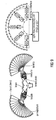
- the main limit lies in the ability to shift the visual axis. This means that each column of the imaging system will be composed of ten optical channels 300 (ommatidia), like shown in Fig. 7b . Even if such a imaging system or compound eye may have a rather coarse resolution, it is well suited and dedicated to optic flow measurement. In any case, it can be considered as a classical imager yielding an image that can be useful for the human eye.
- Flexible imaging systems may be the building blocks for a realization of fully functional curved compound eyes.
- the optical viewing directions are tuneable according to the radius r of curvature of a supporting structure 500. This will allow to obtain a desired ratio between viewing angle and field-of-view of the individual ommatidia, repeatable across the whole compound eye.
- curved compound eyes e.g., cylindrical compound eyes (see Fig. 8b ), active or actuated compound eyes wherein a cylindrical compound eye is endowed with scanning movements, spherical eyes (see Fig. 8c ) and tape-like compound eyes (see Fig. 8d ).
- the cylindrical compound eye shown in Fig. 8b may offer a very large field-of-view in the horizontal plane (up to 360°).
- the vertical columns of ommatidia - when not diced - may be designed to display a slight difference in pitch between the photoreceptor and microlenses (see Fig. 4a , right), such that the vertical field-of-view could span up to 60°, even without adding vertical curvature.
- the cavity of a cylindrical compound eye may offer space for encasing processing units and small actuators. A great advantage may be seen in the free space for components in the eye cavity, which may result in very compact and self-sufficient sensing devices.
- the plurality of optical channels 300 is overall arranged in a two-dimensional array of optical channels, wherein neighbouring rows 530 of optical channels are mechanically separated.
- ommatidia 300 seems to be the easiest way of providing a 2D field of view using only 1D flexibility at the level of the substrate 200. Since a detection of fast motion-related events shall be detected, bio-inspired electronic architectures ( Fig. 9 , right) featuring distributed analog-to-digital converters (ADC) and programmable processing units may be used. This may enable fast visual signal acquisition and local processing before sending the information further to a central processor for global visual processing.
- a micro-controller may be integrated at the column level to process locally the optic flow. In the case where a column is composed of more than 1 pixel (2D retina), a local microcontroller could process the optic flow measured by each vertical ommatidia.
- a programmable processing unit microcontroller or FPGA may be added to process all the incoming signals and compute global information.
- the active, or actuated compound eye may be seen as an cylindrical eye augmented with a device providing a very small minimum visibile (i.e., the smallest area distinctly perceivable by the eye) and an outstanding hyper acuity (Viollet and Franceschini 2001, Viollet and Franceschini 2005). These two properties, rarely encountered in any artificial visual sensor, will rely on the ability of the physical sensor to generate controlled vibrations.
- piezo and artificial muscles or shape memory alloy (SMA). Piezoelectric actuators are widely used due to their high speed, high resolution, good mechanical durability, high output force and low power consumption (Tao et al., 2007).
- piezo bender actuators have been widely used in academic studies and industrial applications, e.g., as piezoelectric switch, valve, pump, ultrasonic motor, printer head, piezoelectric fan, piezoelectric tube scanner and quick focusing lenses (e.g, Yoo et al., 2000).
- the success of piezo technology relies on its high bandwidth (e.g, about 500 Hz). This means that piezo actuators can be controlled in open loop, leading to a drastic simplification of the control electronics.
- the necessary high voltage electronics required for actuating piezo actuators is often complex and bulky. These requirements also limit the use of piezoactuators in autonomous micro-robots (Stelz et al., 2006).
- a possible realization of a spherical compound eye ( Fig. 8c ) consists of arranging several ommatidia patches around a sphere, thus enabling a truly omnidirectional field of view and providing extra free space in the eye cavity for additional components, such as accelerometers and rate gyros, which are necessary for some types of motion-related analysis.
- additional components such as accelerometers and rate gyros, which are necessary for some types of motion-related analysis.
- the rotational component of optic flow which does not correlate with distance to surrounding objects, can be discounted if the rotational components of the eyes are available from 3-axis rate gyroscopes ( Rodriguez, A., Andersen, E., Bradley, J. and Taylor, C. (2007) Wind Estimation Using an Optical Flow Sensor on a Miniature Air Vehicle.
- a lightweight artificial spherical compound eye can cover a truly omnidirectional field of view in order to emulate the visual capabilities of insects.
- a series of circular PCBs may be used or several lines of ommatidia may be arranged directly onto a spherical surface ( Fig. 8c ).
- the former option may facilitate the interconnection of the ommatidia, whereas the latter could be easier to integrate onto the surface of a vehicle or a robot.
- the inertial sense is of high importance to interpret visual information such as optic flow
- the free space available within the spherical compound eye may be exploited to add a set of inertial sensors: 3-axes gyroscopes and 3-axes accelerometers.
- Tapes of elongated and flexible compound eyes may consist of bendable printed circuits embroiled with multiple ommatidia, to be attached to various surfaces or sewed into clothes.
- the plurality of optical channels 300 is arranged in a one-dimensional array of optical channels, wherein neighbouring optical channels are mechanically separated.
- Adding other components may also be considered, such as wireless modules and batteries, which could be soldered on the tape, for making it energetically self-sufficient and capable of communicating motion-related information to other devices.
- the viewing directions of the ommatidia is determined by the underlying surface and not fixed at fabrication time.
- Elongated vision-tapes can be attached onto various flat and curved surfaces or sewed into clothes in order to perceive motion-related information in divergent directions. Unlike standard cameras, which occupy a volume because of their single lens architecture, this vision-tape may cover a significantly wider surface of several centimeters while being only a few micrometers thick. This skin-like property may allow covering widely divergent viewing directions (depending on the underlying surface) while remaining almost unnoticeable from a mechanical point of view.
- the first one would consist of replicating patches of ommatidia produced according to embodiments of the present invention and solder them on top of a second flexible PCB of larger size.
- the second approach would be to pick and place each single ommatidium from its production substrate onto the longer flexible PCB.
- the first approach is simpler in terms of assembly procedure, but the tape may end up not being homogeneously populated with ommatidia and the thickness may be greater due to the superposition of two layers of flex PCB in some places.
- the second approach instead may involve dissolving the glue that has been used in the ommatidia production process (once they have been diced apart from each other), carefully pick them one by one and gluing them onto the larger PCB before they can be wirebonded and encapsulated. Although time consuming, this latter approach could allow more freedom in the way the ommatidia can be spread across the tape, which would represent an advantage.
- a final form of the vision-tape should include thin batteries and a means of sending out motion-related information via wired or wireless communication.
- Fig. 9 Another important aspect of fully functional compound eyes is the design of the readout circuitry and built-in micro-processing units.
- the fly's visual system (Fig. 9 , left), which is composed of a series of neuropils responsible for successive visual processing tasks (local pre-processing -> local motion detection -> global interpretation of motion fields)
- the use of a network of interconnected microcontrollers (Fig. 9 , right) may be considered that may be directly soldered onto the flexible substrate of the ommatidia patches.
- the local microcontrollers can be used to pre-process local visual information in order to remove noise, adapt gains, and estimate optic flow among adjacent ommatidia.
- a main processing unit could then integrate the local information processed by the distributed microcontrollers into higher level signals such as global optic-flow fields, distance estimates or ego-motion. All the processing units (e.g. low-power microcontrollers or FPGA) may be fully programmable.
- embodiments of the present invention provide a compound eye imaging system which may be applied to a curved basis with a highly-precise relation between microlenses and photoreceptors which leads to a highly precisely determined sampling angle.
- Microlenses and photoreceptors make up optical channels, wherein a flexible substrate serves as a mechanical connection between neighboring optical channels.
- an opaque sealing compound may be used for optical channel separation.
- the optics comprising the microlenses as well as the image sensors are provided in planar stacking technique. Both layers are combined in planar condition by waferscale or chipscale mounting. Mounting the microlens-layer and the image-sensor-layer in the planar domain and using established methods allows for a highly precise relation between microlenses and photoreceptors in the sub-micron area.
- the bonded components are then attached to the flexible substrate which may, at the same time, serve as a dicing tape.
- the optical channels resulting from microlenses and associated image-sensors are singulated by, e.g., sewing the microlens-photosensor-sandwich, however, without "injuring" the flexible substrate.
- the resulting imaging system gets flexible or bendable, whereas the association microlens-photosensor within the optical channels remains fixed.
- the singulation may be performed via sawing, laser-cutting, etching, etc.
- the obtained flexible imaging device may be bent and/or mounted to a curved basis. Cavities between the separated optical channels may be filled with a hardening sealing compound material, which may be preferably a black material for optically isolating the optical channels.
- the flexible imaging device may be fixed to the curved basis permanently, or may be again separated from it after "freezing" the curvature.
- a completely flexible or actuated form may be envisaged, like it has been explained above. In this case however, the current deformation condition has to be known in order to recognize an object from the image.
- aspects of the present invention have been described with respect to an imaging system it is to be understood that those aspects also serve as a description of a related method for fabricating the imaging system, such that a block or an element of the imaging system may also interpreted as a related step or a feature of a step of the method for fabricating. Also, aspects that have been described in connection with or as a step of a method may also be interpreted as a description of a respective block, or a detail, or a feature of a respective imaging system.
- Embodiments of the invention described that the image sensors are connected to the flexible substrate by wire-bonding are not limited to such a technique, rather other techniques for connecting the image sensors to the flexible substrate may be used, e.g. by trough silicon interconnection (TS-VIAS), gold bands, printed conductive traces, conductive ink. Also other know techniques may be used.
- TS-VIAS trough silicon interconnection
Priority Applications (3)
| Application Number | Priority Date | Filing Date | Title |
|---|---|---|---|
| AT09012409T ATE538406T1 (de) | 2009-09-30 | 2009-09-30 | Verfahren zur herstellung eines künstliches facettenauges |
| EP09012409A EP2306230B1 (fr) | 2009-09-30 | 2009-09-30 | Procédé de fabrication d'un oeil composé artificiel |
| PCT/EP2010/063741 WO2011039062A1 (fr) | 2009-09-30 | 2010-09-17 | Oeil composé artificiel et son procédé de fabrication |
Applications Claiming Priority (1)
| Application Number | Priority Date | Filing Date | Title |
|---|---|---|---|
| EP09012409A EP2306230B1 (fr) | 2009-09-30 | 2009-09-30 | Procédé de fabrication d'un oeil composé artificiel |
Publications (2)
| Publication Number | Publication Date |
|---|---|
| EP2306230A1 true EP2306230A1 (fr) | 2011-04-06 |
| EP2306230B1 EP2306230B1 (fr) | 2011-12-21 |
Family
ID=41382353
Family Applications (1)
| Application Number | Title | Priority Date | Filing Date |
|---|---|---|---|
| EP09012409A Not-in-force EP2306230B1 (fr) | 2009-09-30 | 2009-09-30 | Procédé de fabrication d'un oeil composé artificiel |
Country Status (3)
| Country | Link |
|---|---|
| EP (1) | EP2306230B1 (fr) |
| AT (1) | ATE538406T1 (fr) |
| WO (1) | WO2011039062A1 (fr) |
Cited By (7)
| Publication number | Priority date | Publication date | Assignee | Title |
|---|---|---|---|---|
| CN102201422A (zh) * | 2011-04-26 | 2011-09-28 | 格科微电子(上海)有限公司 | 凹面cmos图像传感器及其制造方法 |
| US20120242837A1 (en) * | 2011-03-24 | 2012-09-27 | Kabushiki Kaisha Topcon | Omnidirectional Camera |
| US20130160822A1 (en) * | 2011-12-22 | 2013-06-27 | Hon Hai Precision Industry Co., Ltd. | Solar cell system |
| WO2014057104A1 (fr) * | 2012-10-12 | 2014-04-17 | Fraunhofer-Gesellschaft zur Förderung der angewandten Forschung e.V. | Capteur d'images et système de formation d'images optique |
| CN104580869A (zh) * | 2013-10-10 | 2015-04-29 | 华为技术有限公司 | 一种光场相机 |
| CN107872630A (zh) * | 2017-12-25 | 2018-04-03 | 信利光电股份有限公司 | 一种图像传感器 |
| US20220407994A1 (en) * | 2019-11-26 | 2022-12-22 | (Shanghai Institute Of Microsystem And Information Technology,Chinese Academy Ofsciences) | Compound eye camera device and compound eye system |
Families Citing this family (5)
| Publication number | Priority date | Publication date | Assignee | Title |
|---|---|---|---|---|
| DE102012202207B4 (de) * | 2012-02-14 | 2017-02-16 | Paul Metzger | Kamera und Bildaufnahmeverfahren |
| US9113829B2 (en) | 2013-03-27 | 2015-08-25 | Google Inc. | Systems and methods for encapsulating electronics in a mountable device |
| US9488837B2 (en) | 2013-06-28 | 2016-11-08 | Microsoft Technology Licensing, Llc | Near eye display |
| CN117204808A (zh) * | 2017-06-14 | 2023-12-12 | 苏州四海通仪器有限公司 | 一种复眼眼底相机 |
| CN108803016B (zh) * | 2018-06-11 | 2022-08-30 | 北京理工大学 | 基于双焦距透镜和液体透镜的变焦窝区成像方法及系统 |
Citations (4)
| Publication number | Priority date | Publication date | Assignee | Title |
|---|---|---|---|---|
| WO1999026419A1 (fr) * | 1997-11-14 | 1999-05-27 | Tangen Reidar E | Camera optoelectronique et procede de formatage d'images dans ladite camera |
| JP2003283932A (ja) * | 2002-03-25 | 2003-10-03 | Japan Science & Technology Corp | 複眼画像入力装置 |
| WO2005069607A1 (fr) * | 2004-01-20 | 2005-07-28 | Frauhofer-Gesellschaft Zur Förderung Der Angewandten Forschung E.V. | Systeme de capture d'images et utilisation |
| US20060044451A1 (en) * | 2004-08-30 | 2006-03-02 | Eastman Kodak Company | Wide angle lenslet camera |
Family Cites Families (1)
| Publication number | Priority date | Publication date | Assignee | Title |
|---|---|---|---|---|
| US8077235B2 (en) * | 2008-01-22 | 2011-12-13 | Palo Alto Research Center Incorporated | Addressing of a three-dimensional, curved sensor or display back plane |
-
2009
- 2009-09-30 AT AT09012409T patent/ATE538406T1/de active
- 2009-09-30 EP EP09012409A patent/EP2306230B1/fr not_active Not-in-force
-
2010
- 2010-09-17 WO PCT/EP2010/063741 patent/WO2011039062A1/fr active Application Filing
Patent Citations (4)
| Publication number | Priority date | Publication date | Assignee | Title |
|---|---|---|---|---|
| WO1999026419A1 (fr) * | 1997-11-14 | 1999-05-27 | Tangen Reidar E | Camera optoelectronique et procede de formatage d'images dans ladite camera |
| JP2003283932A (ja) * | 2002-03-25 | 2003-10-03 | Japan Science & Technology Corp | 複眼画像入力装置 |
| WO2005069607A1 (fr) * | 2004-01-20 | 2005-07-28 | Frauhofer-Gesellschaft Zur Förderung Der Angewandten Forschung E.V. | Systeme de capture d'images et utilisation |
| US20060044451A1 (en) * | 2004-08-30 | 2006-03-02 | Eastman Kodak Company | Wide angle lenslet camera |
Non-Patent Citations (28)
| Title |
|---|
| BAKER, E. ET AL.: "A spherical eye from multiple cameras (makes better models of the world)", IEEE ROBOTICS AND AUTOMATION MAGAZINE: SPECIAL ISSUE ON PANORAMIC ROBOTS, vol. 11, no. 4, 2004, pages 31 - 38 |
| BRUTTING, W.: "Physics of Organic Semiconductors", 2005, WILEY-VCH |
| COURBON, J. ET AL.: "A generic fisheye camera model for robotic applications", INT. CONF. ON INTELLIGENT ROBOTS AND SYSTEMS, 2007, pages 1683 - 1688 |
| DAHMEN, H.; MILLERS, A.; MALLOT, H.A.: "Insect inspired odometry by optic flow recorded with optical mouse chips, to appear in Flying Robots and Insects", 2009, SPRINGER VERLAG |
| DELBRÜCK, T.; MEAD, C.: "Analog VLSI phototransduction by continuous-time, adaptive, logarithmic photoreceptor circuits", IEEE COMPUTER SOCIETY PRESS, 1995, pages 139 - 161 |
| DUPARRÉ, J. ET AL.: "Artificial apposition compound eye fabricated by micro-optics technology", APPLIED OPTICS, vol. 43, no. 22, 2004, pages 4303 - 4310 |
| DUPARRÉ, J. ET AL.: "Chirped arrays of refractive ellipsoidal microlenses for aberration correction under oblique incidence", OPT. EXP., vol. 13, no. 26, 2005, pages 10539 - 10551 |
| DUPARRÉ, J. ET AL.: "Thin compound eye camera", APPLIED OPTICS, vol. 44, no. 15, 2005, pages 2949 - 2956 |
| DUPARRÉ, J.; WIPPERMANN, F.: "Micro-optical artificial compound eyes", BIOINSPIR. BIOMIM., vol. 1, 2006, pages R1 - R16 |
| GLUCKMAN, J.; NAYAR, S.K.: "Ego-Motion and Omnidirectional Cameras", INT. CONFERENCE ON COMPUTER VISION, 1998, pages 999 - 1005 |
| HORNSEY, R. ET AL.: "Electronic compound eye image sensor: construction and calibration. SPIE International conference on Sensors and Camera Systems for Scientific", INDUSTRIAL, AND DIGITAL PHOTOGRAPHY APPLICATIONS, vol. 5301, 2004, pages 13 - 24 |
| HORRIDGE, G., A., THE COMPOUND EYE OF INSECTS. SCI. AM., vol. 237, 1977, pages 108 - 120 |
| JEONG, K.-H.; KIM, J.; LEE, L.P.: "Biologically Inspired Artificial Compound Eyes", SCIENCE, vol. 312, 2006, pages 557 - 561 |
| KIM, D.-H. ET AL.: "Materials and non- coplanar mesh designs for integrated circuits with linear elastic responses to extreme mechanical deformations", PNAS, vol. 105, no. 48, 2008, pages 18675 - 18680 |
| KIRSCHFELD, K.: "The absolute sensitivity of lens and compound eyes", Z. NATURFORSCH., vol. 29, 1974, pages 592 - 596 |
| KO, H. C. ET AL.: "A hemispherical electronic eye camera based on compressible silicon optoelectronics", NATURE, vol. 454, 2008, pages 748 - 753 |
| LAND, M., VISUAL ACUITY IN INSECTS. ANNUAL REVIEW OF ENTOMOLOGY, vol. 42, 1997, pages 147 - 177 |
| LAND, M.; NILSSON, D.-E.: "Animal Eyes. Oxford animal biology series", 2002, OXFORD UNIVERSITY PRESS |
| LIU, S. ET AL., ANALOG VLSI: CIRCUITS AND PRINCIPLES. MIT PRESS, CAMBRIDGE, MA, 2003 |
| MEI, C.; RIVERS, P.: "Single view point ominidirectional camera calibration", IEEE CONF. ON ROBOTICS AND AUTOMATION, 2007, pages 3945 - 3950 |
| RADTKE, D. ET AL.: "Laser lithographic fabrication and characterization of a spherical artificial compound eye", OPT. EXP., vol. 15, no. 6, 2007, pages 3067 - 3077 |
| RODRIGUEZ, A. ET AL.: "Wind Estimation Using an Optical Flow Sensor on a Miniature Air Vehicle. AIAA Conference on Guidance, Navigation, and Control; Zufferey, J.-C. and Floreano, D. (2006) Fly-inspired Visual Steering of an Ultralight Indoor Aircraft", IEEE TRANSACTIONS ON ROBOTICS, vol. 22, no. 1, 2007, pages 137 - 146 |
| SAITO H ET AL: "Compound eye shaped flexible organic image sensor with a tunable visual field", MICRO ELECTRO MECHANICAL SYSTEMS, 2005. MEMS 2005. 18TH IEEE INTERNATI ONAL CONFERENCE ON MIAMI BEACH, FL, USA JAN. 30 - FEB. 3, 2005, PISCATAWAY, NJ, USA,IEEE, 30 January 2005 (2005-01-30), pages 96 - 99, XP010811668, ISBN: 978-0-7803-8732-4 * |
| SAITO, H. ET AL.: "Compound eye shaped flexible organic image sensor with tunable visual field", IEEE INTERNATIONAL CONFERENCE ON MICRO ELECTRO MECHANICAL SYSTEMS, vol. 1, 2005, pages 96 - 99 |
| VASSALLO, R.F.; SANTOS-VICTOR, J.; SCHNEEBELI, H.J.: "A general approach for egomotion estimation with omnidirectional images", OMNIVIS'02 WORKSHOP ON OMNI-DIRECTIONAL VISION, 2002, pages 97 - 103 |
| VOLKEL R ET AL: "Miniaturized imaging systems", MICROELECTRONIC ENGINEERING, ELSEVIER PUBLISHERS BV., AMSTERDAM, NL, vol. 67-68, 1 June 2003 (2003-06-01), pages 461 - 472, XP004428906, ISSN: 0167-9317 * |
| XU, X. ET AL.: "Direct transfer patterning on three dimensionally deformed surfaces at micrometer resolutions and its application to hemispherical focal plane detector arrays", ORGANIC ELECTRONICS, vol. 9, 2008, pages 1122 - 1127 |
| ZUFFEREY, J.-C.; BEYELER, A.; FLOREANO, D.: "Optic Flow to Steer and Avoid Collisions in 3D. In Flying Insects and Robots", 2009, SPRINGER-VERLAG |
Cited By (11)
| Publication number | Priority date | Publication date | Assignee | Title |
|---|---|---|---|---|
| US20120242837A1 (en) * | 2011-03-24 | 2012-09-27 | Kabushiki Kaisha Topcon | Omnidirectional Camera |
| US8885016B2 (en) | 2011-03-24 | 2014-11-11 | Kabushiki Kaisha Topcon | Omnidirectional camera and lens hood |
| US8934019B2 (en) * | 2011-03-24 | 2015-01-13 | Kabushiki Kaisha Topcon | Omnidirectional camera |
| US9071767B2 (en) | 2011-03-24 | 2015-06-30 | Kabushiki Kaisha Topcon | Omnidirectional camera |
| CN102201422A (zh) * | 2011-04-26 | 2011-09-28 | 格科微电子(上海)有限公司 | 凹面cmos图像传感器及其制造方法 |
| US20130160822A1 (en) * | 2011-12-22 | 2013-06-27 | Hon Hai Precision Industry Co., Ltd. | Solar cell system |
| WO2014057104A1 (fr) * | 2012-10-12 | 2014-04-17 | Fraunhofer-Gesellschaft zur Förderung der angewandten Forschung e.V. | Capteur d'images et système de formation d'images optique |
| CN104580869A (zh) * | 2013-10-10 | 2015-04-29 | 华为技术有限公司 | 一种光场相机 |
| US10321033B2 (en) | 2013-10-10 | 2019-06-11 | Huawei Technologies Co., Ltd. | Light field camera |
| CN107872630A (zh) * | 2017-12-25 | 2018-04-03 | 信利光电股份有限公司 | 一种图像传感器 |
| US20220407994A1 (en) * | 2019-11-26 | 2022-12-22 | (Shanghai Institute Of Microsystem And Information Technology,Chinese Academy Ofsciences) | Compound eye camera device and compound eye system |
Also Published As
| Publication number | Publication date |
|---|---|
| EP2306230B1 (fr) | 2011-12-21 |
| ATE538406T1 (de) | 2012-01-15 |
| WO2011039062A1 (fr) | 2011-04-07 |
Similar Documents
| Publication | Publication Date | Title |
|---|---|---|
| EP2306230B1 (fr) | Procédé de fabrication d'un oeil composé artificiel | |
| Cheng et al. | Review of state-of-the-art artificial compound eye imaging systems | |
| US9426362B2 (en) | Three-axis OIS for super-resolution imaging | |
| US8629353B2 (en) | Apparatus and method using patterned array with separated islands | |
| US20180190704A1 (en) | Methods and applications of non-planar imaging arrays | |
| US7443597B2 (en) | Liquid lens with piezoelectric voltage converter | |
| US8372726B2 (en) | Methods and applications of non-planar imaging arrays | |
| US20190243139A1 (en) | Integrated MicroOptic Imager, Processor, and Display | |
| SE527889C2 (sv) | Apparat för avbildning av ett objekt | |
| CN101103308B (zh) | 控制镜头的方法和设备以及含有该控制方法或设备的相机模块 | |
| CN101926171B (zh) | 具有芯片上的多个像素阵列的照相机系统 | |
| US20110026141A1 (en) | Low Profile Camera and Vision Sensor | |
| US20170168199A1 (en) | Method of Producing a Focal Plane Array for a Multi-Aperture Camera Core | |
| JP2007012995A (ja) | 超小型カメラモジュール及びその製造方法 | |
| US20090321861A1 (en) | Microelectronic imagers with stacked lens assemblies and processes for wafer-level packaging of microelectronic imagers | |
| EP1389804A3 (fr) | Capteur d'image CMOS avec des lentilles à gradient d'indice à l'échelle d'une puce | |
| Viollet et al. | Hardware architecture and cutting-edge assembly process of a tiny curved compound eye | |
| Gao et al. | Recent advances in curved image sensor arrays for bioinspired vision system | |
| Leitel et al. | Curved artificial compound-eyes for autonomous navigation | |
| Hoshino et al. | Design and performance of a micro-sized biomorphic compound eye with a scanning retina | |
| Duparré et al. | Method for fabricating an artificial compound eye | |
| Seo et al. | Biomimetic multiaperture imaging systems: A review | |
| Brückner et al. | Microoptical artificial compound eyes | |
| US20240125591A1 (en) | Wide field-of-view metasurface optics, sensors, cameras and projectors | |
| US20230111183A1 (en) | Window assemblies, imaging system including the same, method of manufacturing the imaging system, and electronic apparatus including the imaging system |
Legal Events
| Date | Code | Title | Description |
|---|---|---|---|
| PUAI | Public reference made under article 153(3) epc to a published international application that has entered the european phase |
Free format text: ORIGINAL CODE: 0009012 |
|
| 17P | Request for examination filed |
Effective date: 20100623 |
|
| AK | Designated contracting states |
Kind code of ref document: A1 Designated state(s): AT BE BG CH CY CZ DE DK EE ES FI FR GB GR HR HU IE IS IT LI LT LU LV MC MK MT NL NO PL PT RO SE SI SK SM TR |
|
| AX | Request for extension of the european patent |
Extension state: AL BA RS |
|
| RTI1 | Title (correction) |
Free format text: METHOD FOR FABRICATING AN ARTIFICIAL COMPOUND EYE |
|
| GRAP | Despatch of communication of intention to grant a patent |
Free format text: ORIGINAL CODE: EPIDOSNIGR1 |
|
| RTI1 | Title (correction) |
Free format text: METHOD FOR FABRICATING AN ARTIFICIAL COMPOUND EYE |
|
| GRAS | Grant fee paid |
Free format text: ORIGINAL CODE: EPIDOSNIGR3 |
|
| GRAA | (expected) grant |
Free format text: ORIGINAL CODE: 0009210 |
|
| AK | Designated contracting states |
Kind code of ref document: B1 Designated state(s): AT BE BG CH CY CZ DE DK EE ES FI FR GB GR HR HU IE IS IT LI LT LU LV MC MK MT NL NO PL PT RO SE SI SK SM TR |
|
| REG | Reference to a national code |
Ref country code: GB Ref legal event code: FG4D |
|
| REG | Reference to a national code |
Ref country code: CH Ref legal event code: EP |
|
| REG | Reference to a national code |
Ref country code: AT Ref legal event code: REF Ref document number: 538406 Country of ref document: AT Kind code of ref document: T Effective date: 20120115 |
|
| REG | Reference to a national code |
Ref country code: IE Ref legal event code: FG4D |
|
| REG | Reference to a national code |
Ref country code: DE Ref legal event code: R096 Ref document number: 602009004248 Country of ref document: DE Effective date: 20120308 |
|
| REG | Reference to a national code |
Ref country code: NL Ref legal event code: VDEP Effective date: 20111221 |
|
| PG25 | Lapsed in a contracting state [announced via postgrant information from national office to epo] |
Ref country code: NO Free format text: LAPSE BECAUSE OF FAILURE TO SUBMIT A TRANSLATION OF THE DESCRIPTION OR TO PAY THE FEE WITHIN THE PRESCRIBED TIME-LIMIT Effective date: 20120321 Ref country code: LT Free format text: LAPSE BECAUSE OF FAILURE TO SUBMIT A TRANSLATION OF THE DESCRIPTION OR TO PAY THE FEE WITHIN THE PRESCRIBED TIME-LIMIT Effective date: 20111221 |
|
| LTIE | Lt: invalidation of european patent or patent extension |
Effective date: 20111221 |
|
| PG25 | Lapsed in a contracting state [announced via postgrant information from national office to epo] |
Ref country code: NL Free format text: LAPSE BECAUSE OF FAILURE TO SUBMIT A TRANSLATION OF THE DESCRIPTION OR TO PAY THE FEE WITHIN THE PRESCRIBED TIME-LIMIT Effective date: 20111221 Ref country code: LV Free format text: LAPSE BECAUSE OF FAILURE TO SUBMIT A TRANSLATION OF THE DESCRIPTION OR TO PAY THE FEE WITHIN THE PRESCRIBED TIME-LIMIT Effective date: 20111221 Ref country code: SI Free format text: LAPSE BECAUSE OF FAILURE TO SUBMIT A TRANSLATION OF THE DESCRIPTION OR TO PAY THE FEE WITHIN THE PRESCRIBED TIME-LIMIT Effective date: 20111221 Ref country code: SE Free format text: LAPSE BECAUSE OF FAILURE TO SUBMIT A TRANSLATION OF THE DESCRIPTION OR TO PAY THE FEE WITHIN THE PRESCRIBED TIME-LIMIT Effective date: 20111221 Ref country code: GR Free format text: LAPSE BECAUSE OF FAILURE TO SUBMIT A TRANSLATION OF THE DESCRIPTION OR TO PAY THE FEE WITHIN THE PRESCRIBED TIME-LIMIT Effective date: 20120322 Ref country code: HR Free format text: LAPSE BECAUSE OF FAILURE TO SUBMIT A TRANSLATION OF THE DESCRIPTION OR TO PAY THE FEE WITHIN THE PRESCRIBED TIME-LIMIT Effective date: 20111221 |
|
| PG25 | Lapsed in a contracting state [announced via postgrant information from national office to epo] |
Ref country code: BE Free format text: LAPSE BECAUSE OF FAILURE TO SUBMIT A TRANSLATION OF THE DESCRIPTION OR TO PAY THE FEE WITHIN THE PRESCRIBED TIME-LIMIT Effective date: 20111221 Ref country code: CY Free format text: LAPSE BECAUSE OF FAILURE TO SUBMIT A TRANSLATION OF THE DESCRIPTION OR TO PAY THE FEE WITHIN THE PRESCRIBED TIME-LIMIT Effective date: 20111221 |
|
| PG25 | Lapsed in a contracting state [announced via postgrant information from national office to epo] |
Ref country code: SK Free format text: LAPSE BECAUSE OF FAILURE TO SUBMIT A TRANSLATION OF THE DESCRIPTION OR TO PAY THE FEE WITHIN THE PRESCRIBED TIME-LIMIT Effective date: 20111221 Ref country code: EE Free format text: LAPSE BECAUSE OF FAILURE TO SUBMIT A TRANSLATION OF THE DESCRIPTION OR TO PAY THE FEE WITHIN THE PRESCRIBED TIME-LIMIT Effective date: 20111221 Ref country code: BG Free format text: LAPSE BECAUSE OF FAILURE TO SUBMIT A TRANSLATION OF THE DESCRIPTION OR TO PAY THE FEE WITHIN THE PRESCRIBED TIME-LIMIT Effective date: 20120321 Ref country code: CZ Free format text: LAPSE BECAUSE OF FAILURE TO SUBMIT A TRANSLATION OF THE DESCRIPTION OR TO PAY THE FEE WITHIN THE PRESCRIBED TIME-LIMIT Effective date: 20111221 Ref country code: IS Free format text: LAPSE BECAUSE OF FAILURE TO SUBMIT A TRANSLATION OF THE DESCRIPTION OR TO PAY THE FEE WITHIN THE PRESCRIBED TIME-LIMIT Effective date: 20120421 |
|
| PG25 | Lapsed in a contracting state [announced via postgrant information from national office to epo] |
Ref country code: RO Free format text: LAPSE BECAUSE OF FAILURE TO SUBMIT A TRANSLATION OF THE DESCRIPTION OR TO PAY THE FEE WITHIN THE PRESCRIBED TIME-LIMIT Effective date: 20111221 Ref country code: PL Free format text: LAPSE BECAUSE OF FAILURE TO SUBMIT A TRANSLATION OF THE DESCRIPTION OR TO PAY THE FEE WITHIN THE PRESCRIBED TIME-LIMIT Effective date: 20111221 Ref country code: PT Free format text: LAPSE BECAUSE OF FAILURE TO SUBMIT A TRANSLATION OF THE DESCRIPTION OR TO PAY THE FEE WITHIN THE PRESCRIBED TIME-LIMIT Effective date: 20120423 |
|
| REG | Reference to a national code |
Ref country code: AT Ref legal event code: MK05 Ref document number: 538406 Country of ref document: AT Kind code of ref document: T Effective date: 20111221 |
|
| PLBE | No opposition filed within time limit |
Free format text: ORIGINAL CODE: 0009261 |
|
| STAA | Information on the status of an ep patent application or granted ep patent |
Free format text: STATUS: NO OPPOSITION FILED WITHIN TIME LIMIT |
|
| PG25 | Lapsed in a contracting state [announced via postgrant information from national office to epo] |
Ref country code: DK Free format text: LAPSE BECAUSE OF FAILURE TO SUBMIT A TRANSLATION OF THE DESCRIPTION OR TO PAY THE FEE WITHIN THE PRESCRIBED TIME-LIMIT Effective date: 20111221 |
|
| 26N | No opposition filed |
Effective date: 20120924 |
|
| PG25 | Lapsed in a contracting state [announced via postgrant information from national office to epo] |
Ref country code: IT Free format text: LAPSE BECAUSE OF FAILURE TO SUBMIT A TRANSLATION OF THE DESCRIPTION OR TO PAY THE FEE WITHIN THE PRESCRIBED TIME-LIMIT Effective date: 20111221 |
|
| REG | Reference to a national code |
Ref country code: DE Ref legal event code: R097 Ref document number: 602009004248 Country of ref document: DE Effective date: 20120924 |
|
| PG25 | Lapsed in a contracting state [announced via postgrant information from national office to epo] |
Ref country code: AT Free format text: LAPSE BECAUSE OF FAILURE TO SUBMIT A TRANSLATION OF THE DESCRIPTION OR TO PAY THE FEE WITHIN THE PRESCRIBED TIME-LIMIT Effective date: 20111221 |
|
| PG25 | Lapsed in a contracting state [announced via postgrant information from national office to epo] |
Ref country code: MC Free format text: LAPSE BECAUSE OF NON-PAYMENT OF DUE FEES Effective date: 20120930 Ref country code: ES Free format text: LAPSE BECAUSE OF FAILURE TO SUBMIT A TRANSLATION OF THE DESCRIPTION OR TO PAY THE FEE WITHIN THE PRESCRIBED TIME-LIMIT Effective date: 20120401 |
|
| PG25 | Lapsed in a contracting state [announced via postgrant information from national office to epo] |
Ref country code: FI Free format text: LAPSE BECAUSE OF FAILURE TO SUBMIT A TRANSLATION OF THE DESCRIPTION OR TO PAY THE FEE WITHIN THE PRESCRIBED TIME-LIMIT Effective date: 20111221 |
|
| REG | Reference to a national code |
Ref country code: FR Ref legal event code: ST Effective date: 20130531 |
|
| REG | Reference to a national code |
Ref country code: IE Ref legal event code: MM4A |
|
| PG25 | Lapsed in a contracting state [announced via postgrant information from national office to epo] |
Ref country code: IE Free format text: LAPSE BECAUSE OF NON-PAYMENT OF DUE FEES Effective date: 20120930 |
|
| PG25 | Lapsed in a contracting state [announced via postgrant information from national office to epo] |
Ref country code: FR Free format text: LAPSE BECAUSE OF NON-PAYMENT OF DUE FEES Effective date: 20121001 |
|
| PGFP | Annual fee paid to national office [announced via postgrant information from national office to epo] |
Ref country code: CH Payment date: 20130917 Year of fee payment: 5 |
|
| PG25 | Lapsed in a contracting state [announced via postgrant information from national office to epo] |
Ref country code: MT Free format text: LAPSE BECAUSE OF FAILURE TO SUBMIT A TRANSLATION OF THE DESCRIPTION OR TO PAY THE FEE WITHIN THE PRESCRIBED TIME-LIMIT Effective date: 20111221 |
|
| PG25 | Lapsed in a contracting state [announced via postgrant information from national office to epo] |
Ref country code: TR Free format text: LAPSE BECAUSE OF FAILURE TO SUBMIT A TRANSLATION OF THE DESCRIPTION OR TO PAY THE FEE WITHIN THE PRESCRIBED TIME-LIMIT Effective date: 20111221 |
|
| GBPC | Gb: european patent ceased through non-payment of renewal fee |
Effective date: 20130930 |
|
| PG25 | Lapsed in a contracting state [announced via postgrant information from national office to epo] |
Ref country code: LU Free format text: LAPSE BECAUSE OF NON-PAYMENT OF DUE FEES Effective date: 20120930 Ref country code: SM Free format text: LAPSE BECAUSE OF FAILURE TO SUBMIT A TRANSLATION OF THE DESCRIPTION OR TO PAY THE FEE WITHIN THE PRESCRIBED TIME-LIMIT Effective date: 20111221 |
|
| PG25 | Lapsed in a contracting state [announced via postgrant information from national office to epo] |
Ref country code: HU Free format text: LAPSE BECAUSE OF FAILURE TO SUBMIT A TRANSLATION OF THE DESCRIPTION OR TO PAY THE FEE WITHIN THE PRESCRIBED TIME-LIMIT Effective date: 20090930 Ref country code: GB Free format text: LAPSE BECAUSE OF NON-PAYMENT OF DUE FEES Effective date: 20130930 |
|
| REG | Reference to a national code |
Ref country code: CH Ref legal event code: PL |
|
| PG25 | Lapsed in a contracting state [announced via postgrant information from national office to epo] |
Ref country code: CH Free format text: LAPSE BECAUSE OF NON-PAYMENT OF DUE FEES Effective date: 20140930 Ref country code: LI Free format text: LAPSE BECAUSE OF NON-PAYMENT OF DUE FEES Effective date: 20140930 Ref country code: MK Free format text: LAPSE BECAUSE OF FAILURE TO SUBMIT A TRANSLATION OF THE DESCRIPTION OR TO PAY THE FEE WITHIN THE PRESCRIBED TIME-LIMIT Effective date: 20111221 |
|
| PGFP | Annual fee paid to national office [announced via postgrant information from national office to epo] |
Ref country code: DE Payment date: 20170911 Year of fee payment: 9 |
|
| REG | Reference to a national code |
Ref country code: DE Ref legal event code: R119 Ref document number: 602009004248 Country of ref document: DE |
|
| PG25 | Lapsed in a contracting state [announced via postgrant information from national office to epo] |
Ref country code: DE Free format text: LAPSE BECAUSE OF NON-PAYMENT OF DUE FEES Effective date: 20190402 |