EP2302484A2 - Semiconductor integrated device and control method thereof - Google Patents
Semiconductor integrated device and control method thereof Download PDFInfo
- Publication number
- EP2302484A2 EP2302484A2 EP10009506A EP10009506A EP2302484A2 EP 2302484 A2 EP2302484 A2 EP 2302484A2 EP 10009506 A EP10009506 A EP 10009506A EP 10009506 A EP10009506 A EP 10009506A EP 2302484 A2 EP2302484 A2 EP 2302484A2
- Authority
- EP
- European Patent Office
- Prior art keywords
- reset
- functional blocks
- clock
- signal
- functional block
- Prior art date
- Legal status (The legal status is an assumption and is not a legal conclusion. Google has not performed a legal analysis and makes no representation as to the accuracy of the status listed.)
- Withdrawn
Links
Images
Classifications
-
- G—PHYSICS
- G06—COMPUTING OR CALCULATING; COUNTING
- G06F—ELECTRIC DIGITAL DATA PROCESSING
- G06F1/00—Details not covered by groups G06F3/00 - G06F13/00 and G06F21/00
- G06F1/04—Generating or distributing clock signals or signals derived directly therefrom
- G06F1/10—Distribution of clock signals, e.g. skew
-
- G—PHYSICS
- G06—COMPUTING OR CALCULATING; COUNTING
- G06F—ELECTRIC DIGITAL DATA PROCESSING
- G06F1/00—Details not covered by groups G06F3/00 - G06F13/00 and G06F21/00
- G06F1/24—Resetting means
Definitions
- the present invention relates to a semiconductor integrated device and a control method thereof.
- the present invention relates to a semiconductor integrated device that includes a plurality of functional blocks for carrying out one function, and a control method thereof.
- Japanese Unexamined Patent Application Publication No. 8-185244 discloses a semiconductor integrated device that divides the internal circuits into a plurality of blocks by function and resets the functional blocks by each functional block, and the control method thereof.
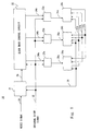
- Fig. 4 illustrates a configuration of a semiconductor integrated device 100 according to a related art.
- a plurality of functional blocks KA to KN are controlled by one control system.
- the semiconductor integrated device 100 includes a selective reset unit 101 which selects and resets the functional block.
- the selective reset unit 101 measures the number of edge or edge interval of a reset signal, and if the measurement result matches any of predetermined setting values, the selective reset unit 101 resets the functional block corresponding to the matched setting value.
- the semiconductor integrated device 100 changes the timing to supply the reset signal to the functional blocks.
- An exemplary aspect of the present invention is a semiconductor integrated device that includes a plurality of functional blocks, a reset signal output unit that outputs a reset signal for resetting the plurality of functional blocks, a clock mask circuit that stops a clock signal, the clock signal being supplied to the plurality of functional blocks, and a clock mask control circuit that controls the supply of the clock signal by the clock mask circuit to the plurality of functional blocks.
- At least one of the functional blocks inputs or outputs a signal with other functional blocks, and the functional blocks are reset when the clock signal and the reset signal are supplied.
- the reset signal output unit supplies the reset signal to the plurality of functional blocks concurrently with or after the clock signal supply to the plurality of functional blocks is stopped.
- the clock mask control circuit sequentially selects one or more of the functional block to reset among the plurality of functional blocks in which the supply of the clock signal is stopped and the reset signal is supplied.
- Another exemplary aspect of the present invention is a control method of a semiconductor integrated device including a plurality of functional blocks in which at least one of the functional blocks inputs or outputs a signal with other functional blocks and the functional blocks are reset when a clock signal and a reset signal are supplied, in which the method includes stopping supply of the clock signal to the plurality of functional blocks, supplying the reset signal to the plurality of functional blocks concurrently with or after stopping the supply of the clock signal, and sequentially selecting one or more of the functional block to reset among the functional blocks in which the supply of the clock signal is stopped and supplied with the reset signal, and supplying the clock signal to the selected functional block.
- the supply of the clock signal to the functional blocks is stopped, so as to stop the signal input or output with other functional block, and thereby preventing a malfunction.
- the reset signal is input to the functional block in which supply of the clock signal is stopped, and the functional block to reset is selected to be supplied with the clock signal.
- the present invention provides a semiconductor integrated device that is capable of selecting one or more among plurality of functional blocks and resetting the selected functional block, and the control method of the semiconductor integrated device.
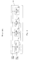
- Fig. 1 is a block diagram illustrating a semiconductor integrated device 20.
- the semiconductor integrated device 20 includes a plurality of functional blocks 24a to 24c, and a reset signal output unit 21 which outputs a* reset signal 36 for resetting the functional blocks 24a to 24c.
- the semiconductor integrated device 20 further includes clock mask circuits 23a to 23c which stop clock signals 35a to 35c supplied to the functional blocks 24a to 24c, and a clock mask control circuit 22 the supply of the clock signals 35a to 35c by the clock mask circuits 23a to 23c to the functional blocks 24a to 24c.
- At least one of the functional blocks 24a to 24c inputs or outputs control signals 37a to 37c, and the functional blocks reset when the clock signals 35a to 35c and the reset signal 36 are supplied.
- the reset signal output unit 21 is connected to the clock mask control circuit 22 and each functional blocks 24a to 24c (hereinafter referred to as the functional block 24 when not necessary to distinguish the functional blocks 24a to 24c).
- the reset signal output unit 21 is supplied with an original clock signal 32, which is a clock signal, and synchronizes with the original clock signal 32 to operate.
- the original clock signal 32 is externally supplied or output by a clock generation circuit (not illustrated) which is mounted inside the semiconductor integrated device 20.
- the reset signal output unit 21 receives a reset request 31.
- the reset request 31 is supplied from outside the system (not illustrated) that includes the semiconductor integrated device 20 mounted therein or supplied internally.
- the reset request 31 is generated at an arbitrary timing when a user wishes to initialize a function of a certain circuit.
- the reset signal output unit 21 In response to the input reset request 31, the reset signal output unit 21 generates a mask control signal 33 to output to the clock mask control circuit 22, and the reset signal 36 to output to the functional blocks 24a to 24c.
- the reset signal output unit 21 outputs the reset signal 36 to each of the functional block 24a to 24c at the same time as or after outputting the mask control signal 33 to the clock mask control circuit 22.
- the clock mask control circuit 22 is connected to the reset signal output unit 21 and the clock mask circuits 23a to 23c.
- the clock mask control circuit 22 generates clock mask signals 34a to 34c according to the mask control signal 33 output by the reset signal output unit 21, and outputs the generated clock mask signals 34a to 34c respectively to the clock mask circuits 23a to 23c. Further, the clock mask control circuit 22 is supplied with the original clock signal 32, and synchronizes with the original clock signal 32 to operate.
- the clock mask circuits 23a to 23c are connected to the clock mask control circuit 22 and connected respectively to the functional blocks 24a to 24c.
- the clock mask circuits 23a to 23c (hereinafter referred to as the clock mask circuit 23 when not necessary to distinguish the clock mask circuits 23a to 23c) are disposed for each functional block. Therefore, the number of clock mask circuit 23 is determined by the number of functional block 24 to be connected. In this exemplary embodiment, the number of functional block 24 is three, thus three clock mask circuits 23 are disposed correspondingly. Note that there may be only one clock mask circuit 23 to control the supply of the clock signal 35 to all the functional blocks 24.
- the clock mask circuits 23a to 23c supply and stop supplying the clock signals 35a to 35c (hereinafter referred to as the clock signal 35 when not necessary to distinguish the clock signal 35a to 35c) to be respectively supplied to the functional blocks 24a to 24c according to the clock mask signals 34a to 34c.
- the clock mask circuit 23 may be composed of an AND circuit, for example.
- the functional blocks 24a to 24c are connected to each other, also to the reset signal output unit 21, and respectively connected to the clock mask circuits 23a to 23c.
- the functional blocks 24a to 24c are reset when the clock signals 35a to 35c and the reset signal 36 are supplied.
- the functional blocks 24a to 24c each receive the reset signal 36 from the reset signal output unit 21 and the clock signals 35a to 35c from the clock mask circuits 23a to 23c.
- the functional blocks 24a to 24c are the internal circuits in LSI divided by function.
- the functional blocks 24a to 24c receive the control signals 37a to 37c output by other functional blocks 24a to 24c, and the functional blocks together operate to perform one function.
- the reset signal output unit 21 stops supplying the clock signals 35a to 35c to the functional blocks 24a to 24c, and supplies the reset signal 36 to the functional block 24 at the same timing as stopping the supply of the clock signals 35a to 35c.
- the clock mask control circuit 22 stops supplying the clock signals 35a to 35c, sequentially selects the functional block 24 to reset from the functional blocks 24a to 24c which are supplied with the reset signal 36, and supplies the clock signals 35a to 35c to the selected functional block 24.
- the reset request 31 is externally input to the reset signal output unit 21.
- the reset signal output unit 21 In response to the reset request 31, the reset signal output unit 21 outputs the mask control signal 33 to the clock mask control circuit 22.
- the clock mask control circuit 22 outputs the clock mask signals 34a to 34c to the clock mask circuits 23a to 23c.
- the clock mask circuits 23a to 23c stop supplying the clock signals 35a to 35c to the functional blocks 24a to 24c according to the clock mask signals 34a to 34c. In response to this, the functional blocks 24a to 24c stop operation.
- the reset signal output unit 21 supplies the reset signal 36 to the functional blocks 24a to 24c at the same time as stopping the supply of the clock signals 35a to 35c to the functional blocks 24a to 24c. Note that the reset signal 36 may not be supplied at the same time as stopping the supply of the clock signal 35 but may be after or concurrently with stopping the supply of the clock signal 35.
- the clock mask control circuit 22 sequentially selects the functional block 24 to reset from the functional blocks 24a to 24c which are supplied with the reset signal 36.
- the case is explained hereinafter in which the functional blocks 24a, 24b, and 24c are selected in this order.
- the clock mask control circuit 22 sequentially supplies the clock signals 35a to 35c for the amount necessary to reset the selected functional blocks 24a to 24c.
- the clock mask control circuit 22 controls the supply of the clock mask signal 34a, in order to supply the clock signal 35a for the amount necessary to reset the functional block 24a.
- the clock mask circuit 23a supplies the functional block 24a with the clock signal 35a for resetting the functional block 24a by combining the original clock signal 32 and the clock mask signal 34a.
- the functional block 24a is reset when the clock signal 35a is supplied.
- the clock signals 35b and 35c for the amount necessary to reset the other functional blocks 24b and 24c are sequentially supplied to the other functional blocks 24b and 24c according to the clock mask signal output by the clock mask control circuit, and the functional blocks 24b and 24c are reset.
- the interval to supply the clock signal 35 to other functional block 24 to reset next is more than or equal to the time required for the current generated due to the influence of resetting the functional block 24 is reduced.
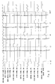
- Fig. 3 is a timing chart according to this exemplary embodiment.
- the reset request 31 is activated at a timing t1 (low active) and input to the reset signal output unit 21.
- the reset signal output unit 21 sets the mask control signal 33 to high-level at the timing t2, and at the same time, activates the reset signal 36 (low active).
- the clock mask control unit 22 which received the mask control signal 33 activates (low active) the clock mask signals 34a to 34c at almost the same time as the input of the mask control signal 33, and then outputs the clock mask signals 34a to 34c to the clock mask circuits 23a to 23c.
- the clock mask circuit 23 stops supplying the clock signals 35a to 35c to the functional blocks 24a to 24c according to the clock mask signals 34a to 34c.
- the clock mask signal control circuit 22 sets the clock mask signal 34a to high-level (low active) only for one clock. Since the clock mask signal 34a is set to high-level (low active) only for one clock at the timing t3, the clock signal 35a is supplied to the functional block 24a for only one clock at the same timing t3.
- the control signal 37a is initialized as well.
- the clock signal 35b and the clock signal 35c are not respectively supplied to the functional block 24b and the functional block 24c, and the functional blocks 24b and 24c are not operating, there is no influence caused by the change in the control signal 37a.
- the remaining functional block 24 is sequentially reset at the timings t4 and t5. Note that only the clock signals 35a to 35c for one clock are illustrated for each of the functional blocks 24a to 24c in Fig. 3 , however the clock signals 35a to 35c for two clocks or more may be supplied.
- the reset request 31 is set to high-level (low active) at the timing t6.
- the reset signal output unit 21 sets the reset signal 36 to high-level (low active) at the timing t7, and at the same time, sets the mask control signal 33 to low-level (high active) and also sets the clock mask signal 34a to 34c output by the clock mask control circuit 22 to high-level (low active). Then the reset is completed.
- the functional block since the functional block is not supplied with the clock signal except at the timing to be reset, the functional blocks not performing reset operation stops the operation. Therefore, even if there are a plurality of functional blocks operating by inputting or outputting signals to each other, the functional blocks will not be influenced by the signals from other functional blocks, and thus there is no possibility of generating a malfunction when resetting the functional blocks. Accordingly, one or more arbitrary functional blocks can be selected and sequentially reset, and thereby preventing an overcurrent from flowing in the circuit.
- a semiconductor integrated device 20 has the same circuit configuration as the first exemplary embodiment, the timing to supply the clock signal 35 is different from the first exemplary embodiment.
- the clock mask control circuit 22 supplies the clock signals 35a to 35c to the selected functional blocks 24a to 24c for the amount necessary to reset.
- the clock mask control circuit 22 of the second exemplary embodiment sequentially starts supplying the clock signal 35 to the selected functional block 24.
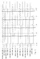
- Fig. 3 is a timing chart according to the second exemplary embodiment.
- the second exemplary embodiment is same as the first exemplary embodiment except the following point, thus the repeated explanation is omitted.
- the point is that the clock signals 35a to 35c are input to the functional block 24 to reset and the functional block 24 which has completed to reset along with the change in the timings to output the clock mask signals 34a to 34c.
- the clock mask signal control circuit 22 sets the clock mask signal 34a to high-level (low active) at the timing t3.
- the clock mask circuit 23a supplies the clock signal 35a to the functional block 24a at the timing t3.
- the clock mask circuit 23a continues to supply the clock signal 35a to the functional block 24a, unlike the first exemplary embodiment in which only the necessary amount of the clock signal 35a to reset is supplied.
- the functional block 24b is reset at the timing t4 in a similar manner as the functional block 24a.
- the reset signal 36 is low level (low active) and the clock signal 35a is supplied when the functional block 24b is reset at the timing t4. Therefore, the functional block 24a is reset every time. However, after the functional block 24a is reset once at the beginning, the functional block 24a which has already reset is reset again, and thus there is no operation actually performed. Moreover, since the reset is repeated each time, the control signal 37 supplied from other functional block 24 is disregarded, and the functional block 24a is not controlled by the other functional blocks. Accordingly, even if the clock signal is supplied to the functional block 24a, no malfunction is generated by the operation of the other functional blocks.
- the functional block 24c is reset at the timing t5.
- the initialization of all the functional block 24 is completed at the timing t6, and at the same time, the reset request 31 is set to high-level (low active).
- the reset signal output unit 21 sets the reset signal 36 to high-level (low active) at the timing t7, and at the same time, sets the mask control signal 33 to low-level (high active). Then the reset is completed.
- operation clocks are received in the order of the functional blocks 24a, 24b, and 24c in Fig. 3 , it is not limited to this.
- control of the clock mask signal 34 is easier than the first exemplary embodiment.
- the clock signals are supplied only to the functional blocks being reset and the functional blocks already reset.
- the signals input and output between the functional blocks and thereby not causing a malfunction at the time of resetting the functional blocks.
- one or more arbitrary functional blocks can be sequentially selected and reset, so as to prevent an overcurrent from flowing in the circuit.
- the first and second exemplary embodiments can be combined as desirable by one of ordinary skill in the art.
Landscapes
- Engineering & Computer Science (AREA)
- Theoretical Computer Science (AREA)
- Physics & Mathematics (AREA)
- General Engineering & Computer Science (AREA)
- General Physics & Mathematics (AREA)
- Semiconductor Integrated Circuits (AREA)
- Design And Manufacture Of Integrated Circuits (AREA)
- Microcomputers (AREA)
Abstract
Description
- This application is based upon and claims the benefit of priority from Japanese patent application No.
2009-217058, filed on September 18, 2009 - The present invention relates to a semiconductor integrated device and a control method thereof. In particular, the present invention relates to a semiconductor integrated device that includes a plurality of functional blocks for carrying out one function, and a control method thereof.
- When resetting a system LSI, since the internal circuits of the system LSI are activated at a time, a large current is instantaneously generated. The current value is proportional to the circuit size. Therefore, along with the increased size of the system LSI, the current generated inside the system LSI also increases at the time of reset. As a result, a power supply voltage drop generated inside the system LSI circuit causes unstable operation, and thereby disabling to reset correctly sometimes.
- If the current generated inside the system LSI circuit increases, higher specifications are required for an external power supply circuit of the system LSI in terms of the current variation and a maximum current value at the time of reset. This seriously affects when building the system including such system LSI.
- For such problem, Japanese Unexamined Patent Application Publication No.
8-185244 (Hanaoka Fig. 4 illustrates a configuration of a semiconductor integrateddevice 100 according to a related art. In the semiconductor integrateddevice 100 of the related art, a plurality of functional blocks KA to KN are controlled by one control system. The semiconductor integrateddevice 100 includes aselective reset unit 101 which selects and resets the functional block. Theselective reset unit 101 measures the number of edge or edge interval of a reset signal, and if the measurement result matches any of predetermined setting values, theselective reset unit 101 resets the functional block corresponding to the matched setting value. At the time of resetting the functional blocks KA to KN, the semiconductor integrateddevice 100 changes the timing to supply the reset signal to the functional blocks. By selecting the functional blocks KA to KN and resetting the selected functional block, it is possible to prevent activation of the internal circuits at a time, and a large current from flowing inside the internal circuits. - However, in the technique disclosed by Hanaoka, even when a part of the blocks are in a reset state, other blocks continue to operate. In the case of the plurality of functional blocks performing one operation, the functional blocks operate by inputting or outputting signals to each other. If only a part of the functional blocks are reset, the signal output to the functional block operating normally from the functional block already reset will be abnormal, and the signal output to the functional block already reset from the functional operating normally will also be abnormal. Therefore, the signals input or output between the functional block already reset and the functional block operating normally could cause a malfunction in the functional block. Accordingly, it is necessary to divide the functional blocks to the extent not to influence mutual operations. The present inventor has found a problem that in the case of the system LSI in which the functional blocks input or output signals with each other, the functional blocks cannot be divided and reset by each functional block.
- An exemplary aspect of the present invention is a semiconductor integrated device that includes a plurality of functional blocks, a reset signal output unit that outputs a reset signal for resetting the plurality of functional blocks, a clock mask circuit that stops a clock signal, the clock signal being supplied to the plurality of functional blocks, and a clock mask control circuit that controls the supply of the clock signal by the clock mask circuit to the plurality of functional blocks. At least one of the functional blocks inputs or outputs a signal with other functional blocks, and the functional blocks are reset when the clock signal and the reset signal are supplied. The reset signal output unit supplies the reset signal to the plurality of functional blocks concurrently with or after the clock signal supply to the plurality of functional blocks is stopped. Further, the clock mask control circuit sequentially selects one or more of the functional block to reset among the plurality of functional blocks in which the supply of the clock signal is stopped and the reset signal is supplied.
- Another exemplary aspect of the present invention is a control method of a semiconductor integrated device including a plurality of functional blocks in which at least one of the functional blocks inputs or outputs a signal with other functional blocks and the functional blocks are reset when a clock signal and a reset signal are supplied, in which the method includes stopping supply of the clock signal to the plurality of functional blocks, supplying the reset signal to the plurality of functional blocks concurrently with or after stopping the supply of the clock signal, and sequentially selecting one or more of the functional block to reset among the functional blocks in which the supply of the clock signal is stopped and supplied with the reset signal, and supplying the clock signal to the selected functional block.
- In the present invention, before resetting the functional block, the supply of the clock signal to the functional blocks is stopped, so as to stop the signal input or output with other functional block, and thereby preventing a malfunction. In addition, the reset signal is input to the functional block in which supply of the clock signal is stopped, and the functional block to reset is selected to be supplied with the clock signal. Thus, it is possible to arbitrarily select the functional block among the plurality of functional blocks that input and output signals to each other.
- The present invention provides a semiconductor integrated device that is capable of selecting one or more among plurality of functional blocks and resetting the selected functional block, and the control method of the semiconductor integrated device.
- The above and other exemplary aspects, advantages and features will be more apparent from the following description of certain exemplary embodiments taken in conjunction with the accompanying drawings, in which:
-
Fig. 1 is a block diagram illustrating a semiconductor integrated device according to a first exemplary embodiment; -
Fig. 2 is a timing chart according to the first exemplary embodiment; -
Fig. 3 is a timing chart according to a second exemplary embodiment; and -
Fig. 4 illustrates a semiconductor integrated device according to a related art. - Hereinafter, exemplary embodiments of the present invention are described with reference to the drawings.
Fig. 1 is a block diagram illustrating a semiconductor integrateddevice 20. The semiconductor integrateddevice 20 according to this exemplary embodiment includes a plurality offunctional blocks 24a to 24c, and a resetsignal output unit 21 which outputs a*reset signal 36 for resetting thefunctional blocks 24a to 24c. The semiconductor integrateddevice 20 further includesclock mask circuits 23a to 23c whichstop clock signals 35a to 35c supplied to thefunctional blocks 24a to 24c, and a clockmask control circuit 22 the supply of theclock signals 35a to 35c by theclock mask circuits 23a to 23c to thefunctional blocks 24a to 24c. At least one of thefunctional blocks 24a to 24c inputs oroutputs control signals 37a to 37c, and the functional blocks reset when the clock signals 35a to 35c and thereset signal 36 are supplied. - The reset
signal output unit 21 is connected to the clockmask control circuit 22 and eachfunctional blocks 24a to 24c (hereinafter referred to as the functional block 24 when not necessary to distinguish thefunctional blocks 24a to 24c). The resetsignal output unit 21 is supplied with anoriginal clock signal 32, which is a clock signal, and synchronizes with theoriginal clock signal 32 to operate. Theoriginal clock signal 32 is externally supplied or output by a clock generation circuit (not illustrated) which is mounted inside the semiconductor integrateddevice 20. - The reset
signal output unit 21 receives areset request 31. Thereset request 31 is supplied from outside the system (not illustrated) that includes the semiconductor integrateddevice 20 mounted therein or supplied internally. Thereset request 31 is generated at an arbitrary timing when a user wishes to initialize a function of a certain circuit. - In response to the
input reset request 31, the resetsignal output unit 21 generates amask control signal 33 to output to the clockmask control circuit 22, and thereset signal 36 to output to thefunctional blocks 24a to 24c. The resetsignal output unit 21 outputs thereset signal 36 to each of thefunctional block 24a to 24c at the same time as or after outputting themask control signal 33 to the clockmask control circuit 22. - The clock
mask control circuit 22 is connected to the resetsignal output unit 21 and theclock mask circuits 23a to 23c. The clockmask control circuit 22 generatesclock mask signals 34a to 34c according to themask control signal 33 output by the resetsignal output unit 21, and outputs the generatedclock mask signals 34a to 34c respectively to theclock mask circuits 23a to 23c. Further, the clockmask control circuit 22 is supplied with theoriginal clock signal 32, and synchronizes with theoriginal clock signal 32 to operate. - The
clock mask circuits 23a to 23c are connected to the clockmask control circuit 22 and connected respectively to thefunctional blocks 24a to 24c. Theclock mask circuits 23a to 23c (hereinafter referred to as the clock mask circuit 23 when not necessary to distinguish theclock mask circuits 23a to 23c) are disposed for each functional block. Therefore, the number of clock mask circuit 23 is determined by the number of functional block 24 to be connected. In this exemplary embodiment, the number of functional block 24 is three, thus three clock mask circuits 23 are disposed correspondingly. Note that there may be only one clock mask circuit 23 to control the supply of the clock signal 35 to all the functional blocks 24. - The
clock mask circuits 23a to 23c supply and stop supplying the clock signals 35a to 35c (hereinafter referred to as the clock signal 35 when not necessary to distinguish theclock signal 35a to 35c) to be respectively supplied to thefunctional blocks 24a to 24c according to the clock mask signals 34a to 34c. The clock mask circuit 23 may be composed of an AND circuit, for example. - The
functional blocks 24a to 24c are connected to each other, also to the resetsignal output unit 21, and respectively connected to theclock mask circuits 23a to 23c. Thefunctional blocks 24a to 24c are reset when the clock signals 35a to 35c and thereset signal 36 are supplied. Thefunctional blocks 24a to 24c each receive thereset signal 36 from the resetsignal output unit 21 and the clock signals 35a to 35c from theclock mask circuits 23a to 23c. - The
functional blocks 24a to 24c are the internal circuits in LSI divided by function. Thefunctional blocks 24a to 24c receive the control signals 37a to 37c output by otherfunctional blocks 24a to 24c, and the functional blocks together operate to perform one function. There is no limitation in the number of division of the functional blocks. The larger the number of division is, the smaller the current will be at the time of initialization. Moreover, the smaller the number of division is, the shorter the time required to initialize the entire functional blocks. Note that in this exemplary embodiment, the number of the functional block 24 is three, however it is not limited to this, and may be two or more than three. - An operation of the semiconductor integrated
device 20 at the time of resetting thefunctional blocks 24a to 24c is explained. The resetsignal output unit 21 stops supplying the clock signals 35a to 35c to thefunctional blocks 24a to 24c, and supplies thereset signal 36 to the functional block 24 at the same timing as stopping the supply of the clock signals 35a to 35c. The clockmask control circuit 22 stops supplying the clock signals 35a to 35c, sequentially selects the functional block 24 to reset from thefunctional blocks 24a to 24c which are supplied with thereset signal 36, and supplies the clock signals 35a to 35c to the selected functional block 24. - The operation of the semiconductor integrated
device 20 at the time of resetting thefunctional blocks 24a to 24c is further explained. First, thereset request 31 is externally input to the resetsignal output unit 21. - In response to the
reset request 31, the resetsignal output unit 21 outputs themask control signal 33 to the clockmask control circuit 22. - The clock
mask control circuit 22 outputs the clock mask signals 34a to 34c to theclock mask circuits 23a to 23c. - The
clock mask circuits 23a to 23c stop supplying the clock signals 35a to 35c to thefunctional blocks 24a to 24c according to the clock mask signals 34a to 34c. In response to this, thefunctional blocks 24a to 24c stop operation. - The reset
signal output unit 21 supplies thereset signal 36 to thefunctional blocks 24a to 24c at the same time as stopping the supply of the clock signals 35a to 35c to thefunctional blocks 24a to 24c. Note that thereset signal 36 may not be supplied at the same time as stopping the supply of the clock signal 35 but may be after or concurrently with stopping the supply of the clock signal 35. - Next, the clock
mask control circuit 22 sequentially selects the functional block 24 to reset from thefunctional blocks 24a to 24c which are supplied with thereset signal 36. For example, the case is explained hereinafter in which thefunctional blocks - In this exemplary embodiment, the clock
mask control circuit 22 sequentially supplies the clock signals 35a to 35c for the amount necessary to reset the selectedfunctional blocks 24a to 24c. - The clock
mask control circuit 22 controls the supply of theclock mask signal 34a, in order to supply theclock signal 35a for the amount necessary to reset thefunctional block 24a. - The
clock mask circuit 23a supplies thefunctional block 24a with theclock signal 35a for resetting thefunctional block 24a by combining theoriginal clock signal 32 and theclock mask signal 34a. - The
functional block 24a is reset when theclock signal 35a is supplied. - After the
functional block 24a is reset, in a similar manner, the clock signals 35b and 35c for the amount necessary to reset the otherfunctional blocks functional blocks functional blocks - By repeating to reset by the interval more than or equal to the time in which the current generated due to the influence of reset reduced it is possible to prevent an overcurrent from flowing in the functional block 24.
- Lastly, the
reset request 31 is canceled, thereset signal 36 is deactivated, and the reset of thefunctional blocks 24a to 24c is completed. - The operation of the semiconductor integrated
device 20 is further described in detail.Fig. 3 is a timing chart according to this exemplary embodiment. First, thereset request 31 is activated at a timing t1 (low active) and input to the resetsignal output unit 21. - In response to the
reset request 31, the resetsignal output unit 21 sets themask control signal 33 to high-level at the timing t2, and at the same time, activates the reset signal 36 (low active). The clockmask control unit 22 which received themask control signal 33 activates (low active) the clock mask signals 34a to 34c at almost the same time as the input of themask control signal 33, and then outputs the clock mask signals 34a to 34c to theclock mask circuits 23a to 23c. The clock mask circuit 23 stops supplying the clock signals 35a to 35c to thefunctional blocks 24a to 24c according to the clock mask signals 34a to 34c. - If the supply of the clock signal 35 to all the functional blocks 24 is stopped, and the
reset signal 36 is input to all the functional blocks 24, the clock masksignal control circuit 22 sets theclock mask signal 34a to high-level (low active) only for one clock. Since theclock mask signal 34a is set to high-level (low active) only for one clock at the timing t3, theclock signal 35a is supplied to thefunctional block 24a for only one clock at the same timing t3. - When the
functional block 24a is initialized, thecontrol signal 37a is initialized as well. However, as theclock signal 35b and theclock signal 35c are not respectively supplied to thefunctional block 24b and thefunctional block 24c, and thefunctional blocks control signal 37a. - When completing to reset the
functional block 24a, in a similar manner, the remaining functional block 24 is sequentially reset at the timings t4 and t5. Note that only the clock signals 35a to 35c for one clock are illustrated for each of thefunctional blocks 24a to 24c inFig. 3 , however the clock signals 35a to 35c for two clocks or more may be supplied. - When the initialization of all the functional blocks 24 is completed, the
reset request 31 is set to high-level (low active) at the timing t6. Then, the resetsignal output unit 21 sets thereset signal 36 to high-level (low active) at the timing t7, and at the same time, sets themask control signal 33 to low-level (high active) and also sets theclock mask signal 34a to 34c output by the clockmask control circuit 22 to high-level (low active). Then the reset is completed. - In this exemplary embodiment, since the functional block is not supplied with the clock signal except at the timing to be reset, the functional blocks not performing reset operation stops the operation. Therefore, even if there are a plurality of functional blocks operating by inputting or outputting signals to each other, the functional blocks will not be influenced by the signals from other functional blocks, and thus there is no possibility of generating a malfunction when resetting the functional blocks. Accordingly, one or more arbitrary functional blocks can be selected and sequentially reset, and thereby preventing an overcurrent from flowing in the circuit.
- Although a semiconductor integrated
device 20 according to a second exemplary embodiment has the same circuit configuration as the first exemplary embodiment, the timing to supply the clock signal 35 is different from the first exemplary embodiment. In the first exemplary embodiment, the clockmask control circuit 22 supplies the clock signals 35a to 35c to the selectedfunctional blocks 24a to 24c for the amount necessary to reset. On the other hand, the clockmask control circuit 22 of the second exemplary embodiment sequentially starts supplying the clock signal 35 to the selected functional block 24. -
Fig. 3 is a timing chart according to the second exemplary embodiment. The second exemplary embodiment is same as the first exemplary embodiment except the following point, thus the repeated explanation is omitted. The point is that the clock signals 35a to 35c are input to the functional block 24 to reset and the functional block 24 which has completed to reset along with the change in the timings to output the clock mask signals 34a to 34c. - The operations till stopping the supply of the clock signal 35 to the functional block 24 and supplying the
reset signal 36 to the functional block 24 which has stopped operation are same as the first exemplary embodiment. - At the timing t2, the supply of the clock signal 35 to the functional block 24 is stopped, and the
reset signal 36 is supplied to all the functional block 24.. Then, the clock masksignal control circuit 22 sets theclock mask signal 34a to high-level (low active) at the timing t3. At the same time as theclock mask signal 34a is set to high-level (low active), theclock mask circuit 23a supplies theclock signal 35a to thefunctional block 24a at the timing t3. At this time, in the second exemplary embodiment, theclock mask circuit 23a continues to supply theclock signal 35a to thefunctional block 24a, unlike the first exemplary embodiment in which only the necessary amount of theclock signal 35a to reset is supplied. - The
functional block 24b is reset at the timing t4 in a similar manner as thefunctional block 24a. - As the
clock mask signal 34a is set to high-level (low active) at the timing t3, in thefunctional block 24a, thereset signal 36 is low level (low active) and theclock signal 35a is supplied when thefunctional block 24b is reset at the timing t4. Therefore, thefunctional block 24a is reset every time. However, after thefunctional block 24a is reset once at the beginning, thefunctional block 24a which has already reset is reset again, and thus there is no operation actually performed. Moreover, since the reset is repeated each time, the control signal 37 supplied from other functional block 24 is disregarded, and thefunctional block 24a is not controlled by the other functional blocks. Accordingly, even if the clock signal is supplied to thefunctional block 24a, no malfunction is generated by the operation of the other functional blocks. - The same applies to when the
functional block 24c is reset at the timing t5. In a similar way as the first exemplary embodiment, the initialization of all the functional block 24 is completed at the timing t6, and at the same time, thereset request 31 is set to high-level (low active). Then, the resetsignal output unit 21 sets thereset signal 36 to high-level (low active) at the timing t7, and at the same time, sets themask control signal 33 to low-level (high active). Then the reset is completed. - In a similar way as the first exemplary embodiment, operation clocks are received in the order of the
functional blocks Fig. 3 , it is not limited to this. - In this exemplary embodiment, control of the clock mask signal 34 is easier than the first exemplary embodiment.
- In this exemplary embodiment, the clock signals are supplied only to the functional blocks being reset and the functional blocks already reset. Thus there is no influence by the signals input and output between the functional blocks, and thereby not causing a malfunction at the time of resetting the functional blocks. Accordingly, one or more arbitrary functional blocks can be sequentially selected and reset, so as to prevent an overcurrent from flowing in the circuit.
- The present invention is not limited to the above exemplary embodiments, but can be modified as appropriate without departing from the scope of the present invention.
- The first and second exemplary embodiments can be combined as desirable by one of ordinary skill in the art.
- While the invention has been described in terms of several exemplary embodiments, those skilled in the art will recognize that the invention can be practiced with various modifications within the spirit and scope of the appended claims and the invention is not limited to the examples described above.
- Further, the scope of the claims is not limited by the exemplary embodiments described above.
- Furthermore, it is noted that, Applicant's intent is to encompass equivalents of all claim elements, even if amended later during prosecution.
Claims (12)
- A semiconductor integrated device comprising:a plurality of functional blocks;a reset signal output unit that outputs a reset signal for resetting the plurality of functional blocks;a clock mask circuit that stops a clock signal, the clock signal being supplied to the plurality of functional blocks; anda clock mask control circuit that controls the supply of the clock signal by the clock mask circuit to the plurality of functional blocks, whereinat least one of the functional blocks inputs or outputs a signal with other functional blocks, and the functional blocks are reset when the clock signal and the reset signal are supplied,the reset signal output unit supplies the reset signal to the plurality of functional blocks concurrently with or after the clock signal supply to the plurality of functional blocks is stopped, andthe clock mask control circuit sequentially selects one or more of the functional block to reset among the plurality of functional blocks in which the supply of the clock signal is stopped and the reset signal is supplied.
- The semiconductor integrated device according to Claim 1, wherein the plurality of functional blocks operate together to perform one function.
- The semiconductor integrated device according to Claim 1 or 2, wherein the reset signal output unit supplies the reset signal to the plurality of functional blocks concurrently with or after the supply of the clock signal to the plurality of functional blocks is stopped.
- The semiconductor integrated device according to Claim 1 or 2, wherein the clock mask control circuit sequentially selects the functional block to reset among the plurality of functional blocks in which the clock signal supply is stopped and supplied with the reset signal.
- The semiconductor integrated device according to Claim 1 or 2, wherein the clock mask circuit is disposed for each functional block.
- The semiconductor integrated device according to Claim 4, wherein the clock mask control circuit sequentially supplies the clock signal for an amount necessary to reset the selected functional block.
- The semiconductor integrated device according to Claim 4, wherein the clock mask control circuit sequentially starts supplying the clock signal to the selected functional block.
- A control method of a semiconductor integrated device including a plurality of functional blocks in which at least one of the functional blocks inputs or outputs a signal with other functional blocks and the functional blocks are reset when a clock signal and a reset signal are supplied, the control method comprising:stopping supply of the clock signal to the plurality of functional blocks;supplying the reset signal to the plurality of functional blocks concurrently with or after stopping the supply of the clock signal; andsequentially selecting one or more of the functional block to reset among the functional blocks in which the supply of the clock signal is stopped and supplied with the reset signal, and supplying the clock signal to the selected functional block.
- The control method according to Claim 8, further comprising supplying the reset signal to the plurality of functional blocks concurrently with or after stopping the supply of the clock signal,
- The control method according to Claim 8, wherein the supply and the supply stop of the clock signal to the functional block is performed for each of the functional block.
- The control method according to Claim 8, further comprising sequentially supplying the clock signal for an amount necessary to reset the functional block.
- The control method according to Claim 8, further comprising sequentially starting to supply the clock signal to the plurality of functional blocks.
Applications Claiming Priority (1)
| Application Number | Priority Date | Filing Date | Title |
|---|---|---|---|
| JP2009217058A JP2011065529A (en) | 2009-09-18 | 2009-09-18 | Semiconductor integrated device and control method thereof |
Publications (2)
| Publication Number | Publication Date |
|---|---|
| EP2302484A2 true EP2302484A2 (en) | 2011-03-30 |
| EP2302484A3 EP2302484A3 (en) | 2011-12-07 |
Family
ID=42829954
Family Applications (1)
| Application Number | Title | Priority Date | Filing Date |
|---|---|---|---|
| EP10009506A Withdrawn EP2302484A3 (en) | 2009-09-18 | 2010-09-13 | Semiconductor integrated device and control method thereof |
Country Status (3)
| Country | Link |
|---|---|
| US (1) | US8154325B2 (en) |
| EP (1) | EP2302484A3 (en) |
| JP (1) | JP2011065529A (en) |
Families Citing this family (1)
| Publication number | Priority date | Publication date | Assignee | Title |
|---|---|---|---|---|
| JP6224994B2 (en) | 2013-11-01 | 2017-11-01 | キヤノン株式会社 | Information processing apparatus and control method thereof |
Citations (1)
| Publication number | Priority date | Publication date | Assignee | Title |
|---|---|---|---|---|
| JPH08185244A (en) | 1994-12-28 | 1996-07-16 | Fujitsu Ltd | Method and apparatus for selectively resetting functional blocks |
Family Cites Families (6)
| Publication number | Priority date | Publication date | Assignee | Title |
|---|---|---|---|---|
| US6480967B1 (en) * | 1999-05-21 | 2002-11-12 | Koninklijke Philips Electronics N.V. | Multiple module processing system with reset system independent of reset characteristics of the modules |
| JP3437802B2 (en) * | 1999-08-10 | 2003-08-18 | 株式会社 沖マイクロデザイン | Clock control circuit and error correction circuit using the same |
| JP4883850B2 (en) * | 2001-06-29 | 2012-02-22 | ルネサスエレクトロニクス株式会社 | Semiconductor device |
| JP4831899B2 (en) * | 2001-08-28 | 2011-12-07 | 富士通セミコンダクター株式会社 | Semiconductor integrated circuit and clock control method |
| JP2005157883A (en) * | 2003-11-27 | 2005-06-16 | Oki Electric Ind Co Ltd | Reset circuit |
| US7038506B2 (en) * | 2004-03-23 | 2006-05-02 | Stmicroelectronics Pvt. Ltd. | Automatic selection of an on-chip ancillary internal clock generator upon resetting a digital system |
-
2009
- 2009-09-18 JP JP2009217058A patent/JP2011065529A/en active Pending
-
2010
- 2010-09-13 EP EP10009506A patent/EP2302484A3/en not_active Withdrawn
- 2010-09-17 US US12/884,973 patent/US8154325B2/en active Active
Patent Citations (1)
| Publication number | Priority date | Publication date | Assignee | Title |
|---|---|---|---|---|
| JPH08185244A (en) | 1994-12-28 | 1996-07-16 | Fujitsu Ltd | Method and apparatus for selectively resetting functional blocks |
Also Published As
| Publication number | Publication date |
|---|---|
| JP2011065529A (en) | 2011-03-31 |
| US8154325B2 (en) | 2012-04-10 |
| US20110102027A1 (en) | 2011-05-05 |
| EP2302484A3 (en) | 2011-12-07 |
Similar Documents
| Publication | Publication Date | Title |
|---|---|---|
| CN109428572B (en) | Semiconductor device and power-off method of semiconductor device | |
| US9553595B2 (en) | Clock operation method and circuit | |
| JP7399622B2 (en) | Semiconductor device and semiconductor device control method | |
| JP2011077814A (en) | Semiconductor device, and power supply control method for the same | |
| JP2009301500A (en) | Task processing system and task processing method | |
| US8154325B2 (en) | Semiconductor integrated device and control method thereof | |
| US8823428B2 (en) | Semiconductor device, method for operating the same, and memory system including the same | |
| JP2006251886A (en) | Microcomputer | |
| JP2009205377A (en) | Integrated circuit device having reset control | |
| US7795938B2 (en) | Apparatus and method for generating clock signal | |
| KR20170045058A (en) | Input circuit and electric apparatus including input circuit | |
| US8004321B2 (en) | Method of implementing power-on-reset in power switches | |
| JP2006072777A (en) | Clock distribution circuit in semiconductor logic circuit, and method therefor | |
| JP2007065756A (en) | Clock control circuit, clock control method, semiconductor integrated circuit device, and electronic apparatus | |
| JP4102864B2 (en) | Delay variable circuit | |
| KR100557607B1 (en) | Clock generator | |
| JP4746592B2 (en) | Microcomputer operating with a plurality of power supplies, and method for starting microcomputer | |
| EP4392848B1 (en) | Dynamic reset latency | |
| JP6360320B2 (en) | Semiconductor device | |
| JP6769490B2 (en) | Integrated circuit equipment | |
| US20070159210A1 (en) | Operation mode setting circuit, LSI having operation mode setting circuit, and operation mode setting method | |
| KR20150014281A (en) | IC reset circuit and method thereof | |
| KR100608598B1 (en) | Systems and Methods for Performing Power Sequencing | |
| US9438217B2 (en) | System and method for clocking integrated circuit | |
| JP2004253595A (en) | Semiconductor integrated circuit and skew controlling method |
Legal Events
| Date | Code | Title | Description |
|---|---|---|---|
| PUAI | Public reference made under article 153(3) epc to a published international application that has entered the european phase |
Free format text: ORIGINAL CODE: 0009012 |
|
| AK | Designated contracting states |
Kind code of ref document: A2 Designated state(s): AL AT BE BG CH CY CZ DE DK EE ES FI FR GB GR HR HU IE IS IT LI LT LU LV MC MK MT NL NO PL PT RO SE SI SK SM TR |
|
| AX | Request for extension of the european patent |
Extension state: BA ME RS |
|
| PUAL | Search report despatched |
Free format text: ORIGINAL CODE: 0009013 |
|
| AK | Designated contracting states |
Kind code of ref document: A3 Designated state(s): AL AT BE BG CH CY CZ DE DK EE ES FI FR GB GR HR HU IE IS IT LI LT LU LV MC MK MT NL NO PL PT RO SE SI SK SM TR |
|
| AX | Request for extension of the european patent |
Extension state: BA ME RS |
|
| RIC1 | Information provided on ipc code assigned before grant |
Ipc: G06F 1/24 20060101ALI20111031BHEP Ipc: G06F 1/10 20060101AFI20111031BHEP |
|
| STAA | Information on the status of an ep patent application or granted ep patent |
Free format text: STATUS: THE APPLICATION HAS BEEN WITHDRAWN |
|
| 18W | Application withdrawn |
Effective date: 20120116 |