EP2297973B1 - Ensemble antenne accordable - Google Patents
Ensemble antenne accordable Download PDFInfo
- Publication number
- EP2297973B1 EP2297973B1 EP08774236.7A EP08774236A EP2297973B1 EP 2297973 B1 EP2297973 B1 EP 2297973B1 EP 08774236 A EP08774236 A EP 08774236A EP 2297973 B1 EP2297973 B1 EP 2297973B1
- Authority
- EP
- European Patent Office
- Prior art keywords
- antenna
- variable impedance
- circuit
- impedance circuit
- point
- Prior art date
- Legal status (The legal status is an assumption and is not a legal conclusion. Google has not performed a legal analysis and makes no representation as to the accuracy of the status listed.)
- Active
Links
- 230000007246 mechanism Effects 0.000 claims description 41
- 238000000034 method Methods 0.000 claims description 4
- 239000003990 capacitor Substances 0.000 description 17
- PEZNEXFPRSOYPL-UHFFFAOYSA-N (bis(trifluoroacetoxy)iodo)benzene Chemical compound FC(F)(F)C(=O)OI(OC(=O)C(F)(F)F)C1=CC=CC=C1 PEZNEXFPRSOYPL-UHFFFAOYSA-N 0.000 description 8
- 238000010586 diagram Methods 0.000 description 7
- 230000003071 parasitic effect Effects 0.000 description 3
- 230000005540 biological transmission Effects 0.000 description 2
- 230000000903 blocking effect Effects 0.000 description 2
- 230000001413 cellular effect Effects 0.000 description 2
- 230000003247 decreasing effect Effects 0.000 description 2
- 230000001419 dependent effect Effects 0.000 description 2
- 230000006870 function Effects 0.000 description 2
- 238000003780 insertion Methods 0.000 description 2
- 230000037431 insertion Effects 0.000 description 2
- 238000004891 communication Methods 0.000 description 1
- 230000007423 decrease Effects 0.000 description 1
- 230000005669 field effect Effects 0.000 description 1
- 238000012986 modification Methods 0.000 description 1
- 230000004048 modification Effects 0.000 description 1
- 239000004065 semiconductor Substances 0.000 description 1
Images


Classifications
-
- H—ELECTRICITY
- H01—ELECTRIC ELEMENTS
- H01Q—ANTENNAS, i.e. RADIO AERIALS
- H01Q9/00—Electrically-short antennas having dimensions not more than twice the operating wavelength and consisting of conductive active radiating elements
- H01Q9/04—Resonant antennas
- H01Q9/0407—Substantially flat resonant element parallel to ground plane, e.g. patch antenna
- H01Q9/0442—Substantially flat resonant element parallel to ground plane, e.g. patch antenna with particular tuning means
-
- H—ELECTRICITY
- H01—ELECTRIC ELEMENTS
- H01Q—ANTENNAS, i.e. RADIO AERIALS
- H01Q1/00—Details of, or arrangements associated with, antennas
- H01Q1/12—Supports; Mounting means
- H01Q1/22—Supports; Mounting means by structural association with other equipment or articles
- H01Q1/24—Supports; Mounting means by structural association with other equipment or articles with receiving set
- H01Q1/241—Supports; Mounting means by structural association with other equipment or articles with receiving set used in mobile communications, e.g. GSM
- H01Q1/242—Supports; Mounting means by structural association with other equipment or articles with receiving set used in mobile communications, e.g. GSM specially adapted for hand-held use
- H01Q1/243—Supports; Mounting means by structural association with other equipment or articles with receiving set used in mobile communications, e.g. GSM specially adapted for hand-held use with built-in antennas
-
- H—ELECTRICITY
- H01—ELECTRIC ELEMENTS
- H01Q—ANTENNAS, i.e. RADIO AERIALS
- H01Q9/00—Electrically-short antennas having dimensions not more than twice the operating wavelength and consisting of conductive active radiating elements
- H01Q9/04—Resonant antennas
- H01Q9/0407—Substantially flat resonant element parallel to ground plane, e.g. patch antenna
- H01Q9/0421—Substantially flat resonant element parallel to ground plane, e.g. patch antenna with a shorting wall or a shorting pin at one end of the element
-
- H—ELECTRICITY
- H01—ELECTRIC ELEMENTS
- H01Q—ANTENNAS, i.e. RADIO AERIALS
- H01Q9/00—Electrically-short antennas having dimensions not more than twice the operating wavelength and consisting of conductive active radiating elements
- H01Q9/04—Resonant antennas
- H01Q9/30—Resonant antennas with feed to end of elongated active element, e.g. unipole
- H01Q9/42—Resonant antennas with feed to end of elongated active element, e.g. unipole with folded element, the folded parts being spaced apart a small fraction of the operating wavelength
Definitions
- Embodiments of the present invention relate to an antenna arrangement.
- they relate to an antenna arrangement for a radio transceiver device.
- an antenna arrangement comprising: an antenna comprising a single radiative element wherein the antenna arrangement has a resonant frequency; a first variable impedance circuit connected between ground and a first point of the antenna; and a second variable impedance circuit connected between ground and a second point of the antenna; and a connection from a third point of the antenna element to ground wherein; the first point of the antenna and the second point of the antenna are separated along the length of the antenna and the impedance of the first variable impedance circuit and the second variable impedance circuit control the resonant frequency of the antenna arrangement; and wherein the second variable impedance circuit is connected to the feed of the antenna.
- the overall impedance of the antenna arrangement and therefore the electrical length is dependent upon the combined impedance of the two variable impedance circuits.
- the overall impedance of the antenna arrangement is not limited by either one of the variable impedance circuits or by the impedance of portions of the antenna itself.
- the resonant frequencies of the antenna arrangement can be controlled so as to increase the operational bandwidth of the antenna arrangement. As the increase in operational bandwidth is achieved by the use of additional circuitry this does not substantially increase the volume of the antenna arrangement.
- the first variable impedance circuit may comprise a tuning circuit and a switching mechanism for connecting/disconnecting the tuning circuit to the antenna.
- the switching mechanism may have a plurality of configurations wherein different configurations of the switching mechanism connect a different tuning circuit to the antenna so that the antenna arrangement has a different resonant frequency for different configurations of the switching mechanism.
- the first variable impedance circuit may comprise a continuously variable tuning circuit.
- the second variable impedance circuit may comprise a tuning circuit and a switching mechanism for connecting/disconnecting the tuning circuit to the antenna.
- the switching mechanism may have a plurality of configurations wherein different configurations of the switching mechanism connect a different tuning circuit to the antenna so that the antenna arrangement has a different resonant frequency for different configurations of the switching element.
- the switching mechanism of the second variable impedance circuit may have a configuration in which the tuning circuit is disconnected from the antenna.
- the second variable impedance circuit may comprise a continuously variable tuning circuit.
- variable impedance circuits may be connected to a ground plane.
- the antenna may be an F antenna or a loop antenna.
- a method comprising: controlling the impedance of a first variable impedance circuit connected between ground and a first point of an antenna wherein the antenna is provided within an antenna arrangement and has a resonant frequency and wherein the antenna comprises a single radiative element; controlling the impedance of a second variable impedance circuit connected between ground and a second point of the antenna; providing a connection from a third point of the antenna to ground wherein; the first point of the antenna and the second point of the antenna are separated along the length of the antenna and the impedance of the first variable impedance circuit and the second variable impedance circuit control the resonant frequency of the antenna; and wherein the second variable impedance circuit is connected to the feed of the antenna.
- a module comprising an antenna as described above.
- a portable electronic device comprising an antenna as described above.
- the device may be for wireless communication.
- JP10224142 A discloses a single patch radiator having a resonant frequency which can be tuned by a plurality of impedance matching circuits switchable between shorting pins at the edge of the radiator and ground.
- WO03/065499 A2 shows an antenna having two radiating elements each having an adjustable transmission line for frequency tuning each of the two radiating antenna elements.
- US2003/0174092 A1 discloses a planar inverted-F antenna having an open and a shorted stub at the antenna feed for impedance matching.
- JP 09 307 344 A shows a planar inverted-F antenna including a variable impedance matching circuit connected between the edge of the PIFA and ground.
- the Figures illustrate an antenna arrangement 12 comprising: an antenna 22; a first variable impedance circuit 30 connected between ground and a first point 23 of the antenna 22; and a second variable impedance circuit 34 connected between ground and a second point 25 of the antenna 22; and a connection 62 from a third point 61 of the antenna 22 to ground wherein; the first point 23 of the antenna 22 and the second point 25 of the antenna 22 are separated along the length of the antenna 22 and the impedance of the first variable impedance circuit 30 and the second variable impedance circuit 34 control the resonant frequency of the antenna arrangement 12.
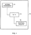
- Fig. 1 schematically illustrates an apparatus 10 comprising an antenna arrangement 12 according to embodiments of the invention.
- the apparatus 10 may be any portable device and may be, for example, a mobile cellular telephone, a personal digital assistant (PDA), a laptop computer, a palm top computer, a portable WLAN or WiFi device, or module for such devices.
- PDA personal digital assistant
- 'module' refers to a unit or apparatus that excludes certain parts/components that would be added by an end manufacturer or a user.
- the apparatus 10 comprises an antenna arrangement 12, a transceiver 14 and functional circuitry 16.
- the functional circuitry 16 comprises a processor, a memory and input/output devices such as a microphone, a loudspeaker, a display and a user input device such as a keypad.
- the transceiver 14 is connected to the functional circuitry 16 and the antenna arrangement 12.
- the functional circuitry 16 is arranged to provide data to the transceiver 14.
- the transceiver 14 is arranged to encode the data and provide it to the antenna arrangement 12 for transmission.
- the antenna arrangement 12 is arranged to transmit the encoded data as a radio signal.
- the antenna arrangement 12 is also arranged to receive a radio signal. The antenna arrangement 12 then provides the received radio signal to the transceiver 14 which decodes the radio signal into data and provides the data to the functional circuitry 16.
- the antenna arrangement 12 may be arranged to operate in a plurality of different operational radio frequency bands and via a plurality of different protocols.
- the different frequency bands and protocols may include (but are not limited to) AM radio (0.535-1.705 MHz); FM radio (76-108 MHz); Bluetooth (2400-2483.5 MHz); WLAN (2400-2483.5 MHz); HLAN (5150-5850 MHz); GPS (1570.42-1580.42 MHz); US-GSM 850 (824-894 MHz); EGSM 900 (880-960 MHz); EU-WCDMA 900 (880-960 MHz); PCN/DCS 1800 (1710-1880 MHz); US-WCDMA 1900 (1850-1990 MHz); WCDMA 2100 (Tx: 1920-1980 MHz Rx: 2110-2180 MHz); PCS1900 (1850-1990 MHz); UWB Lower (3100-4900 MHz); UWB Upper (6000-10600 MHz); DVB-H (470-702 MHz); DVB-H US (1670-1675 MHz); DRM
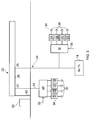
- Fig. 2 is a schematic illustration of an antenna arrangement 12 according to an embodiment of the invention.
- the antenna arrangement 12 comprises an antenna 22, a first variable impedance circuit 30 and a second variable impedance circuit 34.
- the antenna 22 is a PIFA antenna, in other embodiments the antenna element may be any F antenna having a feed point and a connection to ground or a loop antenna.
- the antenna 22 comprises a single radiative element. In other embodiments of the invention the antenna 22 may comprise a plurality of radiative elements which may be galvanically attached to each other or electromagnetically coupled together.
- the antenna 22 is connected to ground 38 via a first point 23.
- This point 23 is also connected to a variable impedance circuit 30 and may be considered to be a tuning connection.
- the antenna is also connected to a feed 24 via a feed point 25.
- the antenna 22 comprises a first portion 26 between the first point 23 and the feed point 25 and a second portion 28 between the feed point 25 and the free end 29 of the antenna 22.
- the antenna 22 also comprises a third connection 62 from a third point 61 of the antenna 22 to ground.
- the third point is in the first portion 26 of the antenna element between the first point 23 and the feed point 25. In other embodiments the third point may be positioned in a different portion of the antenna 22.
- the first variable impedance circuit 30 is connected between ground and the first point 23 of the antenna 22.
- the first variable impedance circuit 30 may be considered to be in series with the first portion 26 of the antenna 22.
- the first control signal 32 controls the impedance of the first variable impedance circuit 30.
- the electrical length of the antenna arrangement 12 depends upon the impedance of the first variable impedance circuit 30.
- the electrical length of the antenna arrangement 12 can be controlled by controlling the impedance of the first variable impedance circuit 30. This enables the antenna arrangement 12 to be tuned to have a particular electrical length and therefore resonate at a particular frequency.
- the impedance of the first variable impedance circuit 30 can be controlled it is connected to the first portion 26 of the antenna 22 which has a fixed impedance.
- the impedance of the first portion 26 therefore imposes a limit on the impedance of the section of the antenna arrangement 12 between the ground 38 and the feed point 25 which consequently imposes a limit on the range of resonant frequencies that can be achieved by the antenna arrangement 12.
- a second variable impedance circuit 34 is connected to the feed point 25 of the antenna 22.
- the feed point 25 is separated from the first point 23 along the length of the antenna 22 by the first portion 26 of the antenna 22.
- the second variable impedance circuit 34 may be considered to be connected in parallel with the first impedance circuit 30 and the first portion 26 of the antenna 22.
- the impedance of the second variable impedance circuit 34 is controlled by the second control signal 36.
- the second variable impedance circuit 34 is connected in parallel to the feed connection 24.
- the second variable impedance circuit 34 may be connected between the transceiver 14 which is providing the feed signal and the feed point 25, that is, the second variable impedance circuit may be in series with the feed connection.
- the second variable impedance circuit 34 may be connected both in parallel to the feed connection 24 and also connected in series between the transceiver 14 and the feed point 25.
- the second variable impedance circuit 34 may comprise two portions a first portion which is connected in parallel to the feed and a second portion which is connected in series.
- the electrical length of the antenna arrangement 12 also depends upon the impedance of the second variable impedance circuit 34.
- the electrical length of the antenna arrangement 12 can be controlled by controlling the impedance of the first variable impedance circuit 30 and/or the second variable impedance circuit 34.
- the impedance of the first portion 26 does not impose a limit on the impedance of the section of the circuit. This means that a greater range of impedances can be achieved by connecting the second variable impedance circuit 34 to the antenna 22 and consequently enables a greater range of operable resonant frequencies to be achieved by the antenna arrangement 12.
- the antenna arrangement 12 can be tuned to resonate at a plurality of different frequencies and so increase the operational bandwidth of the antenna arrangement 12.
- the operational bandwidth of the antenna arrangement 12 is the range of frequencies over which the antenna arrangement 12 can operate efficiently. Efficient operation occurs when the insertion loss of the antenna arrangement is better than an operational threshold such as -6dB.
- Fig. 3 illustrates an antenna arrangement 12 according to a second embodiment of the invention.
- the antenna arrangement 12 of this embodiment of the invention also comprises an antenna 22, a first variable impedance circuit 30 and a second variable impedance circuit 34 connected in the same manner as the embodiment illustrated in Fig. 2 .
- the antenna 22 is a PIFA.
- the PIFA 22 is configured to be operable in two different frequency bands.
- the antenna arrangement 12 comprises a parasitic element 60 which, in this embodiment, couples to the antenna 22 in the high band mode of operation. In other embodiments the parasitic element 60 may couple to the antenna 22 in the low band mode of operation or there may be no parasitic element 60.
- the PIFA has three connections 62, 63 and 24.
- the first connection 62 is a connection direct to ground.
- the second connection 63 is a tuning connection.
- the tuning connection 63 comprises a first variable impedance circuit 30 which is connected between ground and a first point 23 of the antenna 22.
- the third connection 24 is a feed connection and is connected to a second point 25 of the antenna 22.
- the second point 25 is separated from the first point 23 by the first portion 26 of the antenna 22.
- the first variable impedance circuit 30 is connected to ground and comprises a switch mechanism 40 which is configured to connect and disconnect a plurality of tuning circuits 42 to the antenna 22.
- the switch mechanism is an SP4T (single pole 4 throw) switch and enables any one of four different tuning circuits 42 to be connected to the antenna 22.
- the electrical length and therefore the resonant frequency of the antenna arrangement 12 is dependent upon which of the four tuning circuits 42 is connected to the antenna 22.
- the first control signal 32 controls the impedance of the first variable impedance circuit 30 by controlling the configuration of the switch mechanism 40.
- the first variable impedance circuit 30 is connected to the PIFA 22 so that the first variable impedance circuit 30 is in series with a first portion 26 of the PIFA 22.
- the second variable impedance circuit 34 also comprises a switch mechanism 50 which is also configured to connect and disconnect a plurality of tuning circuits 52.
- the switch mechanism 50 connected to the second variable impedance circuit 34 is also an SP4T (single pole 4 throw) switch and also enables any of four different tuning circuits 52 to be connected to the antenna 22.
- the control signal 36 controls the impedance of the second variable impedance circuit 34 by controlling the configuration of the switch mechanism 50.
- the switch mechanism 50 of the second variable impedance circuit 34 has the same number of switch positions as the switch mechanism 40 of the first variable impedance circuit 30.
- the two switch mechanisms 40, 50 may have different numbers of switch positions, for example the first switch mechanism 40 could have four switch positions while the second switch mechanism 50 only has two.
- the second variable impedance circuit 34 is connected to the feed point 25 of the antenna 22 and may be considered to be connected in parallel with the first variable impedance circuit 30 and the first portion 26 of the PIFA.
- the second embodiment of the invention works in the same way as the first embodiment.
- the overall impedance of the antenna arrangement 12 is not limited by the impedance of either of the variable impedance circuits 30, 34 or of any portion of the antenna 22.
- Fig. 4 is a circuit diagram of a variable impedance circuit which may be used as the second variable impedance circuit 34 within embodiments of the invention such as the embodiment illustrated in Fig 3 .
- the switching mechanism 50 is an SP4T switch. Each of the four positions of the switching mechanism 50 connects to a different tuning circuit 52.
- the tuning circuit 52 is connected to ground 38.
- the tuning circuit 52 which comprises a first inductor 80 in parallel with a first capacitor 82, is connected to the antenna 22.
- a second capacitor 84 is connected between ground and the tuning circuit 52.
- the inductor has an inductance of 5.5nH
- the first capacitor has a capacitance of 7pF
- the second capacitor has a capacitance of 100pF.
- the second capacitor 84 acts as a DC blocking component.
- the tuning circuit 52 and capacitor 84 is connected to the antenna 22 in series with a second inductor 86.
- the second inductor 86 has an inductance of 1nH.
- the tuning circuit 52 and capacitor 84 is connected to the antenna 22 in series with a third inductor 88.
- the third inductor 88 has an inductance of 6nH.
- Each of the switch positions therefore connects a different circuit having a different impedance to the antenna 22. Therefore each position of the switch mechanism corresponds to a different electrical length of the antenna arrangement 12 and therefore enables the antenna 22 to resonate at a different resonant frequency.
- variable inductance circuit The values and arrangement of the components of the variable inductance circuit given above are specific to the particular embodiment described. It is to be appreciated that in other embodiments the values of the components of the tuning circuits may be selected so as to enable the antenna arrangement 12 to resonate at a particular frequency and so may have other values. Also the components may be arranged in a different configuration or different components such as microstrip lines, strip lines and delay lines may be used.
- Fig. 5 is a circuit diagram of an embodiment of the invention.
- This embodiment comprises a second variable impedance circuit 34 as illustrated in Fig. 4 connected to an antenna 22.
- the switching mechanism 50 and tuning circuit 52 are as described above with reference to Fig. 4
- the second variable impedance circuit 34 is connected to the feed 24.
- An additional capacitor 100 is connected between the second variable impedance circuit 34 and the feed 24.
- the additional capacitor 100 acts as a DC blocking component.
- the capacitance of the additional capacitor 100 in this specific embodiment is 100pF.
- the first switching mechanism 40 is also an SP4T switch having four switch positions.
- the capacitor 130 is connected to the antenna 22.
- the capacitor has a capacitance of 2pF. The connection of the capacitor 130 to the antenna 22 increases the electrical length of the antenna arrangement 12 and consequently lowers the resonant frequency of the antenna arrangement 12.
- the capacitor 132 When the switch mechanism 40 is configured in the second position 121 the capacitor 132 is connected to the antenna 22.
- the capacitor 132 has a capacitance of 100pF and at radio frequencies is feed through so that this connection acts as a short circuit.
- the capacitor 132 may be omitted and so that the antenna 22 is connected directly to ground.
- the inductor 134 When the switch mechanism 40 is configured in the third position 122 the inductor 134 is connected to the antenna 22.
- the inductor 134 has an inductance of 5.1nH. The connection of the inductor 134 to the antenna 22 decreases the electrical length of the antenna arrangement 12 and consequently increases the resonant frequency of the antenna arrangement 12.
- the switch mechanism 40 When the switch mechanism 40 is configured in the fourth position 123 the antenna element is connected to an open circuit 136.
- An electrostatic discharge (ESD) filter 106 is connected between the switching mechanism 40 and the antenna 22.
- the ESD filter reduces ESD noise in the antenna arrangement 12.
- the ESD filter 106 comprises a capacitor 108 with a capacitance of 8.2pF and an inductor 110 with an inductance of 6.8nH connected in shunt.
- the switching mechanisms 40 and 50 may be semiconductor switches, for example field effect transistors (FETs) or bipolar junction transistors (BJTs), or MEMs (micro electro-mechanical) switches, or mechanical switches, or any kind of switching device.
- FETs field effect transistors
- BJTs bipolar junction transistors
- MEMs micro electro-mechanical switches
Landscapes
- Engineering & Computer Science (AREA)
- Computer Networks & Wireless Communication (AREA)
- Variable-Direction Aerials And Aerial Arrays (AREA)
- Transceivers (AREA)
- Details Of Aerials (AREA)
Claims (13)
- Agencement d'antenne comprenant :une antenne comprenant un seul élément rayonnant dans lequel l'agencement d'antenne a une fréquence de résonnance ;un premier circuit d'impédance variable connecté entre la masse et un premier point de l'antenne ; etun second circuit d'impédance variable connecté entre la masse et un deuxième point de l'antenne et une connexion entre un troisième point de l'antenne et la masse dans lequel :le premier point de l'antenne et le deuxième point de l'antenne sont séparés le long de l'antenne et les impédances du premier circuit d'impédance variable et du second circuit d'impédance variable commandent la fréquence de résonnance de l'agencement d'antenne ;caractérisé en ce que le second circuit d'impédance variable est connecté à la source de l'antenne.
- Agencement d'antenne selon la revendication 1, dans lequel le premier circuit d'impédance variable comprend un circuit d'accord et un mécanisme de commutation pour connecter/déconnecter le circuit d'accord à l'antenne.
- Agencement d'antenne selon la revendication 2, dans lequel le mécanisme de commutation du premier circuit d'impédance variable a une pluralité de configurations, différentes configurations du mécanisme de commutation connectant un circuit d'accord différent à l'antenne de telle sorte que l'agencement d'antenne ait une fréquence de résonnance différente pour différentes configurations du mécanisme de commutation.
- Agencement d'antenne selon la revendication 1, dans lequel au moins l'un des circuits d'impédance variable comprend un circuit d'accord continuellement variable.
- Agencement d'antenne selon l'une quelconque des revendications précédentes, dans lequel le second circuit d'impédance variable comprend un circuit d'accord et un mécanisme de commutation pour connecter/déconnecter le circuit d'accord à l'antenne.
- Agencement d'antenne selon la revendication 5, dans lequel le mécanisme de commutation du second circuit d'impédance variable a une pluralité de configurations, différentes configurations du mécanisme de commutation connectant un circuit d'accord différent à l'antenne de telle sorte que l'agencement d'antenne ait une fréquence de résonnance différente pour différentes configurations du mécanisme de commutation.
- Agencement d'antenne selon la revendication 6, dans lequel le mécanisme de commutation du second circuit d'impédance variable a une configuration dans laquelle le circuit d'accord est déconnecté de l'antenne.
- Agencement d'antenne selon l'une quelconque des revendications précédentes, dans lequel l'antenne est une antenne F ou une antenne cadre.
- Module comprenant une antenne selon l'une quelconque des revendications 1 à 8.
- Dispositif électronique portable comprenant une antenne selon l'une quelconque des revendications 1 à 8.
- Procédé comprenant :la commande de l'impédance d'un premier circuit d'impédance variable connecté entre la masse et un premier point d'une antenne, l'antenne étant fournie dans un agencement d'antenne et ayant une fréquence de résonnance et l'antenne comprenant un seul élément rayonnant ;la commande de l'impédance d'un second circuit d'impédance variable connecté entre la masse et un deuxième point de l'antenne fournissant une connexion entre un troisième point de l'antenne et la masse dans lequel :le premier point de l'antenne et le deuxième point de l'antenne sont séparés le long de l'antenne et les impédances du premier circuit d'impédance variable et du second circuit d'impédance variable commandent la fréquence de résonnance d'un agencement d'antenne comprenant l'antenne ;caractérisé en ce que le second circuit d'impédance variable est connecté à la source de l'antenne.
- Procédé selon la revendication 11, dans lequel l'impédance du premier circuit d'impédance variable est commandée en commandant la configuration d'un mécanisme de commutation pour connecter/déconnecter un circuit d'accord à l'antenne.
- Procédé selon la revendication 11, dans lequel l'impédance du premier circuit d'impédance variable est commandée en faisant varier l'impédance d'un circuit d'accord continuellement variable.
Priority Applications (1)
| Application Number | Priority Date | Filing Date | Title |
|---|---|---|---|
| PL08774236T PL2297973T3 (pl) | 2008-06-23 | 2008-06-23 | Przestrajalny układ antenowy |
Applications Claiming Priority (1)
| Application Number | Priority Date | Filing Date | Title |
|---|---|---|---|
| PCT/EP2008/057977 WO2009155966A1 (fr) | 2008-06-23 | 2008-06-23 | Ensemble antenne accordable |
Publications (2)
| Publication Number | Publication Date |
|---|---|
| EP2297973A1 EP2297973A1 (fr) | 2011-03-23 |
| EP2297973B1 true EP2297973B1 (fr) | 2016-03-16 |
Family
ID=40351856
Family Applications (1)
| Application Number | Title | Priority Date | Filing Date |
|---|---|---|---|
| EP08774236.7A Active EP2297973B1 (fr) | 2008-06-23 | 2008-06-23 | Ensemble antenne accordable |
Country Status (6)
| Country | Link |
|---|---|
| US (1) | US8674889B2 (fr) |
| EP (1) | EP2297973B1 (fr) |
| CN (1) | CN102067624B (fr) |
| ES (1) | ES2572889T3 (fr) |
| PL (1) | PL2297973T3 (fr) |
| WO (1) | WO2009155966A1 (fr) |
Families Citing this family (68)
| Publication number | Priority date | Publication date | Assignee | Title |
|---|---|---|---|---|
| US8744384B2 (en) | 2000-07-20 | 2014-06-03 | Blackberry Limited | Tunable microwave devices with auto-adjusting matching circuit |
| US9406444B2 (en) | 2005-11-14 | 2016-08-02 | Blackberry Limited | Thin film capacitors |
| US7711337B2 (en) | 2006-01-14 | 2010-05-04 | Paratek Microwave, Inc. | Adaptive impedance matching module (AIMM) control architectures |
| US8781522B2 (en) | 2006-11-02 | 2014-07-15 | Qualcomm Incorporated | Adaptable antenna system |
| US7714676B2 (en) | 2006-11-08 | 2010-05-11 | Paratek Microwave, Inc. | Adaptive impedance matching apparatus, system and method |
| US7535312B2 (en) | 2006-11-08 | 2009-05-19 | Paratek Microwave, Inc. | Adaptive impedance matching apparatus, system and method with improved dynamic range |
| US7917104B2 (en) | 2007-04-23 | 2011-03-29 | Paratek Microwave, Inc. | Techniques for improved adaptive impedance matching |
| US8213886B2 (en) | 2007-05-07 | 2012-07-03 | Paratek Microwave, Inc. | Hybrid techniques for antenna retuning utilizing transmit and receive power information |
| US7991363B2 (en) | 2007-11-14 | 2011-08-02 | Paratek Microwave, Inc. | Tuning matching circuits for transmitter and receiver bands as a function of transmitter metrics |
| US20100022192A1 (en) * | 2008-07-24 | 2010-01-28 | Infineon Technologies Ag | Systems and Methods for Transmitter/Receiver Diversity |
| JP2010041071A (ja) * | 2008-07-31 | 2010-02-18 | Toshiba Corp | アンテナ装置 |
| US8072285B2 (en) | 2008-09-24 | 2011-12-06 | Paratek Microwave, Inc. | Methods for tuning an adaptive impedance matching network with a look-up table |
| US20100231461A1 (en) * | 2009-03-13 | 2010-09-16 | Qualcomm Incorporated | Frequency selective multi-band antenna for wireless communication devices |
| US8285231B2 (en) * | 2009-06-09 | 2012-10-09 | Broadcom Corporation | Method and system for an integrated leaky wave antenna-based transmitter and on-chip power distribution |
| US8472888B2 (en) | 2009-08-25 | 2013-06-25 | Research In Motion Rf, Inc. | Method and apparatus for calibrating a communication device |
| US9026062B2 (en) | 2009-10-10 | 2015-05-05 | Blackberry Limited | Method and apparatus for managing operations of a communication device |
| US8803631B2 (en) | 2010-03-22 | 2014-08-12 | Blackberry Limited | Method and apparatus for adapting a variable impedance network |
| US8860525B2 (en) | 2010-04-20 | 2014-10-14 | Blackberry Limited | Method and apparatus for managing interference in a communication device |
| US9379454B2 (en) | 2010-11-08 | 2016-06-28 | Blackberry Limited | Method and apparatus for tuning antennas in a communication device |
| DE112010006094T5 (de) | 2010-12-27 | 2014-06-05 | Epcos Ag | Eingangskreis |
| US8712340B2 (en) | 2011-02-18 | 2014-04-29 | Blackberry Limited | Method and apparatus for radio antenna frequency tuning |
| US8655286B2 (en) | 2011-02-25 | 2014-02-18 | Blackberry Limited | Method and apparatus for tuning a communication device |
| US8594584B2 (en) | 2011-05-16 | 2013-11-26 | Blackberry Limited | Method and apparatus for tuning a communication device |
| CN103931051B (zh) * | 2011-05-16 | 2016-10-26 | 黑莓有限公司 | 用于调谐通信设备的方法和装置 |
| US8626083B2 (en) | 2011-05-16 | 2014-01-07 | Blackberry Limited | Method and apparatus for tuning a communication device |
| CN103636061B (zh) | 2011-07-06 | 2015-12-09 | 诺基亚公司 | 用于无线通信的具有天线的装置以及方法 |
| EP2740221B1 (fr) | 2011-08-05 | 2019-06-26 | BlackBerry Limited | Procédé et appareil pour un réglage de bande dans un dispositif de communication |
| US8776002B2 (en) * | 2011-09-06 | 2014-07-08 | Variable Z0, Ltd. | Variable Z0 antenna device design system and method |
| KR101357724B1 (ko) * | 2011-12-29 | 2014-02-03 | 주식회사 바켄 | 다중 대역 안테나 장치 |
| TWI523316B (zh) * | 2012-03-14 | 2016-02-21 | 宏碁股份有限公司 | 通訊裝置 |
| TWI508365B (zh) * | 2012-05-04 | 2015-11-11 | Yageo Corp | 具有連接電路之天線 |
| US8948889B2 (en) | 2012-06-01 | 2015-02-03 | Blackberry Limited | Methods and apparatus for tuning circuit components of a communication device |
| US9853363B2 (en) | 2012-07-06 | 2017-12-26 | Blackberry Limited | Methods and apparatus to control mutual coupling between antennas |
| US9246223B2 (en) | 2012-07-17 | 2016-01-26 | Blackberry Limited | Antenna tuning for multiband operation |
| US9350405B2 (en) | 2012-07-19 | 2016-05-24 | Blackberry Limited | Method and apparatus for antenna tuning and power consumption management in a communication device |
| US9413066B2 (en) | 2012-07-19 | 2016-08-09 | Blackberry Limited | Method and apparatus for beam forming and antenna tuning in a communication device |
| US9362891B2 (en) | 2012-07-26 | 2016-06-07 | Blackberry Limited | Methods and apparatus for tuning a communication device |
| US10404295B2 (en) | 2012-12-21 | 2019-09-03 | Blackberry Limited | Method and apparatus for adjusting the timing of radio antenna tuning |
| US9374113B2 (en) | 2012-12-21 | 2016-06-21 | Blackberry Limited | Method and apparatus for adjusting the timing of radio antenna tuning |
| KR101372140B1 (ko) * | 2013-01-25 | 2014-03-07 | 엘지이노텍 주식회사 | 안테나 장치 및 그의 급전 구조체 |
| US10594025B2 (en) | 2013-03-11 | 2020-03-17 | Suunto Oy | Coupled antenna structure and methods |
| US10734731B2 (en) | 2013-03-11 | 2020-08-04 | Suunto Oy | Antenna assembly for customizable devices |
| US11059550B2 (en) | 2013-03-11 | 2021-07-13 | Suunto Oy | Diving computer with coupled antenna and water contact assembly |
| US11050142B2 (en) * | 2013-03-11 | 2021-06-29 | Suunto Oy | Coupled antenna structure |
| US9236930B2 (en) * | 2013-06-13 | 2016-01-12 | Nokia Technologies Oy | Methods and apparatus for antenna tuning |
| US9548538B2 (en) * | 2013-06-20 | 2017-01-17 | Sony Corporation | Antenna arrangement and device |
| CN110085994B (zh) * | 2013-11-22 | 2021-08-20 | 华为终端有限公司 | 一种可调天线及终端 |
| US20160191085A1 (en) * | 2014-08-13 | 2016-06-30 | Skyworks Solutions, Inc. | Transmit front end module for dual antenna applications |
| KR20160029539A (ko) * | 2014-09-05 | 2016-03-15 | 엘지전자 주식회사 | 공진주파수 가변 안테나 |
| CN105591198B (zh) * | 2014-10-21 | 2020-07-10 | 深圳富泰宏精密工业有限公司 | 天线结构及具有该天线结构的电子装置 |
| US9438319B2 (en) | 2014-12-16 | 2016-09-06 | Blackberry Limited | Method and apparatus for antenna selection |
| CN106033841A (zh) * | 2015-03-19 | 2016-10-19 | 联想(北京)有限公司 | 天线装置、电子设备和用于天线装置的控制方法 |
| CN104852148A (zh) * | 2015-04-03 | 2015-08-19 | 青岛海信移动通信技术股份有限公司 | 一种可调谐天线及终端 |
| DE102015117170A1 (de) * | 2015-10-08 | 2017-04-13 | Infineon Technologies Ag | Kontaktlos-Schaltkreisanordnung |
| KR102332117B1 (ko) * | 2016-07-21 | 2021-11-30 | 삼성전자주식회사 | 무선 통신을 위한 안테나 및 이를 포함하는 전자 장치 |
| US10998622B2 (en) | 2016-07-21 | 2021-05-04 | Samsung Electronics Co., Ltd | Antenna for wireless communication and electronic device including the same |
| US10290946B2 (en) | 2016-09-23 | 2019-05-14 | Apple Inc. | Hybrid electronic device antennas having parasitic resonating elements |
| CN106935978A (zh) * | 2017-03-13 | 2017-07-07 | 联想(北京)有限公司 | 天线以及移动终端 |
| EP3687187A4 (fr) * | 2017-11-21 | 2020-12-16 | Huawei Technologies Co., Ltd. | Antenne, procédé de commande d'antenne et terminal |
| CN107967026B (zh) * | 2017-11-23 | 2019-10-25 | Oppo广东移动通信有限公司 | 天线组件、终端设备及改善天线辐射性能的方法 |
| TWI790344B (zh) | 2018-02-08 | 2023-01-21 | 芬蘭商順妥公司 | 槽孔模式天線 |
| TWI798344B (zh) | 2018-02-08 | 2023-04-11 | 芬蘭商順妥公司 | 槽孔模式天線 |
| CN109462031A (zh) * | 2018-10-10 | 2019-03-12 | 清华大学 | 基于可变电感和可变电容的双级可调谐天线 |
| CN109586030B (zh) * | 2018-12-25 | 2021-06-29 | 维沃移动通信有限公司 | 一种移动终端及天线控制方法 |
| US10539700B1 (en) | 2019-03-14 | 2020-01-21 | Suunto Oy | Diving computer with coupled antenna and water contact assembly |
| CN112490639B (zh) * | 2019-09-12 | 2022-09-16 | 华为技术有限公司 | 天线装置、通信产品及天线方向图的重构方法 |
| CN111786696A (zh) * | 2020-07-13 | 2020-10-16 | 维沃移动通信有限公司 | 天线调节方法、电路、装置和电子设备 |
| CN113422619B (zh) | 2021-06-18 | 2022-05-27 | 安徽安努奇科技有限公司 | 一种调谐电路及通讯设备 |
Citations (1)
| Publication number | Priority date | Publication date | Assignee | Title |
|---|---|---|---|---|
| JPH10224142A (ja) * | 1997-02-04 | 1998-08-21 | Kenwood Corp | 共振周波数切換え可能な逆f型アンテナ |
Family Cites Families (19)
| Publication number | Priority date | Publication date | Assignee | Title |
|---|---|---|---|---|
| US3818480A (en) * | 1971-07-12 | 1974-06-18 | Magnavox Co | Method and apparatus for controlling the directivity pattern of an antenna |
| US3909830A (en) * | 1974-05-17 | 1975-09-30 | Us Army | Tactical high frequency antenna |
| JPH02236211A (ja) | 1989-03-10 | 1990-09-19 | Kawasaki Steel Corp | ベルレス高炉の炉頂装入方法およびその装置 |
| JP3340621B2 (ja) * | 1996-05-13 | 2002-11-05 | 松下電器産業株式会社 | 平面アンテナ |
| JP3646782B2 (ja) * | 1999-12-14 | 2005-05-11 | 株式会社村田製作所 | アンテナ装置およびそれを用いた通信機 |
| JP2003249811A (ja) * | 2001-12-20 | 2003-09-05 | Murata Mfg Co Ltd | 複共振アンテナ装置 |
| US6650295B2 (en) | 2002-01-28 | 2003-11-18 | Nokia Corporation | Tunable antenna for wireless communication terminals |
| US6819287B2 (en) * | 2002-03-15 | 2004-11-16 | Centurion Wireless Technologies, Inc. | Planar inverted-F antenna including a matching network having transmission line stubs and capacitor/inductor tank circuits |
| GB0209818D0 (en) * | 2002-04-30 | 2002-06-05 | Koninkl Philips Electronics Nv | Antenna arrangement |
| AU2003227707A1 (en) | 2002-05-08 | 2003-11-11 | Sony Ericsson Mobile Communications Ab | Multiple frequency bands switchable antenna for portable terminals |
| EP1729413B1 (fr) | 2004-03-16 | 2015-12-09 | Hitachi Metals, Ltd. | Circuit haute fréquence et composant haute fréquence |
| JP2005303940A (ja) * | 2004-04-16 | 2005-10-27 | Matsushita Electric Ind Co Ltd | アンテナスイッチ回路、ならびにそれを用いた複合高周波部品および移動体通信機器 |
| WO2005109569A1 (fr) | 2004-05-12 | 2005-11-17 | Yokowo Co., Ltd. | Antenne multibande, substrat de circuit et dispositif de communication |
| US7928914B2 (en) * | 2004-06-21 | 2011-04-19 | Motorola Mobility, Inc. | Multi-frequency conductive-strip antenna system |
| JP3889423B2 (ja) * | 2004-12-16 | 2007-03-07 | 松下電器産業株式会社 | 偏波切り替えアンテナ装置 |
| WO2007096693A1 (fr) | 2006-02-22 | 2007-08-30 | Nokia Corporation | Agencement d'antenne |
| CN101496224B (zh) | 2006-07-28 | 2012-12-12 | 株式会社村田制作所 | 天线装置和无线通信设备 |
| JP5531582B2 (ja) * | 2009-11-27 | 2014-06-25 | 富士通株式会社 | アンテナおよび無線通信装置 |
| CN102356514B (zh) * | 2010-01-19 | 2015-01-07 | 松下电器(美国)知识产权公司 | 天线装置和无线通信装置 |
-
2008
- 2008-06-23 ES ES08774236.7T patent/ES2572889T3/es active Active
- 2008-06-23 PL PL08774236T patent/PL2297973T3/pl unknown
- 2008-06-23 CN CN200880129992.0A patent/CN102067624B/zh active Active
- 2008-06-23 US US12/999,454 patent/US8674889B2/en active Active
- 2008-06-23 EP EP08774236.7A patent/EP2297973B1/fr active Active
- 2008-06-23 WO PCT/EP2008/057977 patent/WO2009155966A1/fr active Application Filing
Patent Citations (1)
| Publication number | Priority date | Publication date | Assignee | Title |
|---|---|---|---|---|
| JPH10224142A (ja) * | 1997-02-04 | 1998-08-21 | Kenwood Corp | 共振周波数切換え可能な逆f型アンテナ |
Also Published As
| Publication number | Publication date |
|---|---|
| ES2572889T3 (es) | 2016-06-02 |
| CN102067624A (zh) | 2011-05-18 |
| PL2297973T3 (pl) | 2016-08-31 |
| US8674889B2 (en) | 2014-03-18 |
| WO2009155966A1 (fr) | 2009-12-30 |
| CN102067624B (zh) | 2015-07-01 |
| EP2297973A1 (fr) | 2011-03-23 |
| US20110148723A1 (en) | 2011-06-23 |
Similar Documents
| Publication | Publication Date | Title |
|---|---|---|
| EP2297973B1 (fr) | Ensemble antenne accordable | |
| US7298339B1 (en) | Multiband multimode compact antenna system | |
| US7696928B2 (en) | Systems and methods for using parasitic elements for controlling antenna resonances | |
| EP1932215B1 (fr) | Antenne monopôle courbe multibande | |
| CN101563811B (zh) | 天线布置 | |
| JP4875166B2 (ja) | 2つの素子が共通フィードを共有することを可能にする装置 | |
| EP2645479B1 (fr) | Dispositif de communication et élément d'antenne reconfigurable | |
| US20140015719A1 (en) | Switched antenna apparatus and methods | |
| US8072390B2 (en) | Antenna arrangement | |
| EP2648278B1 (fr) | Antenne interne penta-bande et terminal de communication mobile correspondant | |
| EP2615683A1 (fr) | Dispositif de communication et structure d'antenne correspondante | |
| EP1858115A1 (fr) | Dispositif d'antenne et appareil de radiocommunication portatif utilisant cette antenne | |
| US8378900B2 (en) | Antenna arrangement | |
| WO2013007868A1 (fr) | Agencement d'antenne cadre | |
| KR20070051292A (ko) | 안테나 장치 및 그러한 안테나 장치를 포함하는 휴대무선통신 장치 | |
| CN101507046A (zh) | 多部分无线设备 | |
| KR100830568B1 (ko) | 셀룰러 통신 단말기용 안테나 장치 | |
| EP2639881B1 (fr) | Dispositif de communication et élément d'antenne réglable | |
| US20140354497A1 (en) | Antenna structure and wireless communication device using the same | |
| KR20080089658A (ko) | 안테나 장치 | |
| GB2406217A (en) | Tuneable antenna | |
| CN102931470A (zh) | 多部分无线设备 |
Legal Events
| Date | Code | Title | Description |
|---|---|---|---|
| PUAI | Public reference made under article 153(3) epc to a published international application that has entered the european phase |
Free format text: ORIGINAL CODE: 0009012 |
|
| 17P | Request for examination filed |
Effective date: 20101217 |
|
| AK | Designated contracting states |
Kind code of ref document: A1 Designated state(s): AT BE BG CH CY CZ DE DK EE ES FI FR GB GR HR HU IE IS IT LI LT LU LV MC MT NL NO PL PT RO SE SI SK TR |
|
| AX | Request for extension of the european patent |
Extension state: AL BA MK RS |
|
| DAX | Request for extension of the european patent (deleted) | ||
| RAP1 | Party data changed (applicant data changed or rights of an application transferred) |
Owner name: NOKIA CORPORATION |
|
| 17Q | First examination report despatched |
Effective date: 20150211 |
|
| RAP1 | Party data changed (applicant data changed or rights of an application transferred) |
Owner name: NOKIA TECHNOLOGIES OY |
|
| REG | Reference to a national code |
Ref country code: DE Ref legal event code: R079 Ref document number: 602008042861 Country of ref document: DE Free format text: PREVIOUS MAIN CLASS: H04Q0009040000 Ipc: H01Q0009040000 |
|
| GRAP | Despatch of communication of intention to grant a patent |
Free format text: ORIGINAL CODE: EPIDOSNIGR1 |
|
| RIC1 | Information provided on ipc code assigned before grant |
Ipc: H01Q 9/04 20060101AFI20150818BHEP Ipc: H01Q 1/24 20060101ALI20150818BHEP |
|
| INTG | Intention to grant announced |
Effective date: 20150914 |
|
| GRAS | Grant fee paid |
Free format text: ORIGINAL CODE: EPIDOSNIGR3 |
|
| GRAA | (expected) grant |
Free format text: ORIGINAL CODE: 0009210 |
|
| AK | Designated contracting states |
Kind code of ref document: B1 Designated state(s): AT BE BG CH CY CZ DE DK EE ES FI FR GB GR HR HU IE IS IT LI LT LU LV MC MT NL NO PL PT RO SE SI SK TR |
|
| REG | Reference to a national code |
Ref country code: GB Ref legal event code: FG4D |
|
| REG | Reference to a national code |
Ref country code: CH Ref legal event code: EP |
|
| REG | Reference to a national code |
Ref country code: IE Ref legal event code: FG4D |
|
| REG | Reference to a national code |
Ref country code: AT Ref legal event code: REF Ref document number: 781931 Country of ref document: AT Kind code of ref document: T Effective date: 20160415 |
|
| REG | Reference to a national code |
Ref country code: DE Ref legal event code: R096 Ref document number: 602008042861 Country of ref document: DE |
|
| REG | Reference to a national code |
Ref country code: FR Ref legal event code: PLFP Year of fee payment: 9 |
|
| REG | Reference to a national code |
Ref country code: NL Ref legal event code: FP |
|
| REG | Reference to a national code |
Ref country code: ES Ref legal event code: FG2A Ref document number: 2572889 Country of ref document: ES Kind code of ref document: T3 Effective date: 20160602 |
|
| REG | Reference to a national code |
Ref country code: LT Ref legal event code: MG4D |
|
| PG25 | Lapsed in a contracting state [announced via postgrant information from national office to epo] |
Ref country code: NO Free format text: LAPSE BECAUSE OF FAILURE TO SUBMIT A TRANSLATION OF THE DESCRIPTION OR TO PAY THE FEE WITHIN THE PRESCRIBED TIME-LIMIT Effective date: 20160616 Ref country code: GR Free format text: LAPSE BECAUSE OF FAILURE TO SUBMIT A TRANSLATION OF THE DESCRIPTION OR TO PAY THE FEE WITHIN THE PRESCRIBED TIME-LIMIT Effective date: 20160617 Ref country code: FI Free format text: LAPSE BECAUSE OF FAILURE TO SUBMIT A TRANSLATION OF THE DESCRIPTION OR TO PAY THE FEE WITHIN THE PRESCRIBED TIME-LIMIT Effective date: 20160316 Ref country code: HR Free format text: LAPSE BECAUSE OF FAILURE TO SUBMIT A TRANSLATION OF THE DESCRIPTION OR TO PAY THE FEE WITHIN THE PRESCRIBED TIME-LIMIT Effective date: 20160316 |
|
| REG | Reference to a national code |
Ref country code: AT Ref legal event code: MK05 Ref document number: 781931 Country of ref document: AT Kind code of ref document: T Effective date: 20160316 |
|
| PG25 | Lapsed in a contracting state [announced via postgrant information from national office to epo] |
Ref country code: SE Free format text: LAPSE BECAUSE OF FAILURE TO SUBMIT A TRANSLATION OF THE DESCRIPTION OR TO PAY THE FEE WITHIN THE PRESCRIBED TIME-LIMIT Effective date: 20160316 Ref country code: LV Free format text: LAPSE BECAUSE OF FAILURE TO SUBMIT A TRANSLATION OF THE DESCRIPTION OR TO PAY THE FEE WITHIN THE PRESCRIBED TIME-LIMIT Effective date: 20160316 Ref country code: LT Free format text: LAPSE BECAUSE OF FAILURE TO SUBMIT A TRANSLATION OF THE DESCRIPTION OR TO PAY THE FEE WITHIN THE PRESCRIBED TIME-LIMIT Effective date: 20160316 |
|
| PG25 | Lapsed in a contracting state [announced via postgrant information from national office to epo] |
Ref country code: IS Free format text: LAPSE BECAUSE OF FAILURE TO SUBMIT A TRANSLATION OF THE DESCRIPTION OR TO PAY THE FEE WITHIN THE PRESCRIBED TIME-LIMIT Effective date: 20160716 Ref country code: EE Free format text: LAPSE BECAUSE OF FAILURE TO SUBMIT A TRANSLATION OF THE DESCRIPTION OR TO PAY THE FEE WITHIN THE PRESCRIBED TIME-LIMIT Effective date: 20160316 |
|
| PG25 | Lapsed in a contracting state [announced via postgrant information from national office to epo] |
Ref country code: SK Free format text: LAPSE BECAUSE OF FAILURE TO SUBMIT A TRANSLATION OF THE DESCRIPTION OR TO PAY THE FEE WITHIN THE PRESCRIBED TIME-LIMIT Effective date: 20160316 Ref country code: AT Free format text: LAPSE BECAUSE OF FAILURE TO SUBMIT A TRANSLATION OF THE DESCRIPTION OR TO PAY THE FEE WITHIN THE PRESCRIBED TIME-LIMIT Effective date: 20160316 Ref country code: CZ Free format text: LAPSE BECAUSE OF FAILURE TO SUBMIT A TRANSLATION OF THE DESCRIPTION OR TO PAY THE FEE WITHIN THE PRESCRIBED TIME-LIMIT Effective date: 20160316 Ref country code: PT Free format text: LAPSE BECAUSE OF FAILURE TO SUBMIT A TRANSLATION OF THE DESCRIPTION OR TO PAY THE FEE WITHIN THE PRESCRIBED TIME-LIMIT Effective date: 20160718 Ref country code: RO Free format text: LAPSE BECAUSE OF FAILURE TO SUBMIT A TRANSLATION OF THE DESCRIPTION OR TO PAY THE FEE WITHIN THE PRESCRIBED TIME-LIMIT Effective date: 20160316 |
|
| REG | Reference to a national code |
Ref country code: DE Ref legal event code: R097 Ref document number: 602008042861 Country of ref document: DE |
|
| PG25 | Lapsed in a contracting state [announced via postgrant information from national office to epo] |
Ref country code: BE Free format text: LAPSE BECAUSE OF FAILURE TO SUBMIT A TRANSLATION OF THE DESCRIPTION OR TO PAY THE FEE WITHIN THE PRESCRIBED TIME-LIMIT Effective date: 20160316 Ref country code: IT Free format text: LAPSE BECAUSE OF FAILURE TO SUBMIT A TRANSLATION OF THE DESCRIPTION OR TO PAY THE FEE WITHIN THE PRESCRIBED TIME-LIMIT Effective date: 20160316 |
|
| PLBE | No opposition filed within time limit |
Free format text: ORIGINAL CODE: 0009261 |
|
| STAA | Information on the status of an ep patent application or granted ep patent |
Free format text: STATUS: NO OPPOSITION FILED WITHIN TIME LIMIT |
|
| PG25 | Lapsed in a contracting state [announced via postgrant information from national office to epo] |
Ref country code: MC Free format text: LAPSE BECAUSE OF FAILURE TO SUBMIT A TRANSLATION OF THE DESCRIPTION OR TO PAY THE FEE WITHIN THE PRESCRIBED TIME-LIMIT Effective date: 20160316 Ref country code: DK Free format text: LAPSE BECAUSE OF FAILURE TO SUBMIT A TRANSLATION OF THE DESCRIPTION OR TO PAY THE FEE WITHIN THE PRESCRIBED TIME-LIMIT Effective date: 20160316 |
|
| REG | Reference to a national code |
Ref country code: CH Ref legal event code: PL |
|
| 26N | No opposition filed |
Effective date: 20161219 |
|
| PG25 | Lapsed in a contracting state [announced via postgrant information from national office to epo] |
Ref country code: BG Free format text: LAPSE BECAUSE OF FAILURE TO SUBMIT A TRANSLATION OF THE DESCRIPTION OR TO PAY THE FEE WITHIN THE PRESCRIBED TIME-LIMIT Effective date: 20160616 |
|
| REG | Reference to a national code |
Ref country code: IE Ref legal event code: MM4A |
|
| PG25 | Lapsed in a contracting state [announced via postgrant information from national office to epo] |
Ref country code: LI Free format text: LAPSE BECAUSE OF NON-PAYMENT OF DUE FEES Effective date: 20160630 Ref country code: CH Free format text: LAPSE BECAUSE OF NON-PAYMENT OF DUE FEES Effective date: 20160630 |
|
| REG | Reference to a national code |
Ref country code: FR Ref legal event code: PLFP Year of fee payment: 10 |
|
| PG25 | Lapsed in a contracting state [announced via postgrant information from national office to epo] |
Ref country code: IE Free format text: LAPSE BECAUSE OF NON-PAYMENT OF DUE FEES Effective date: 20160623 Ref country code: SI Free format text: LAPSE BECAUSE OF FAILURE TO SUBMIT A TRANSLATION OF THE DESCRIPTION OR TO PAY THE FEE WITHIN THE PRESCRIBED TIME-LIMIT Effective date: 20160316 |
|
| REG | Reference to a national code |
Ref country code: FR Ref legal event code: PLFP Year of fee payment: 11 |
|
| PG25 | Lapsed in a contracting state [announced via postgrant information from national office to epo] |
Ref country code: HU Free format text: LAPSE BECAUSE OF FAILURE TO SUBMIT A TRANSLATION OF THE DESCRIPTION OR TO PAY THE FEE WITHIN THE PRESCRIBED TIME-LIMIT; INVALID AB INITIO Effective date: 20080623 Ref country code: CY Free format text: LAPSE BECAUSE OF FAILURE TO SUBMIT A TRANSLATION OF THE DESCRIPTION OR TO PAY THE FEE WITHIN THE PRESCRIBED TIME-LIMIT Effective date: 20160316 |
|
| PG25 | Lapsed in a contracting state [announced via postgrant information from national office to epo] |
Ref country code: LU Free format text: LAPSE BECAUSE OF NON-PAYMENT OF DUE FEES Effective date: 20160623 Ref country code: MT Free format text: LAPSE BECAUSE OF NON-PAYMENT OF DUE FEES Effective date: 20160630 Ref country code: TR Free format text: LAPSE BECAUSE OF FAILURE TO SUBMIT A TRANSLATION OF THE DESCRIPTION OR TO PAY THE FEE WITHIN THE PRESCRIBED TIME-LIMIT Effective date: 20160316 |
|
| P01 | Opt-out of the competence of the unified patent court (upc) registered |
Effective date: 20230527 |
|
| PGFP | Annual fee paid to national office [announced via postgrant information from national office to epo] |
Ref country code: ES Payment date: 20230712 Year of fee payment: 16 |
|
| PGFP | Annual fee paid to national office [announced via postgrant information from national office to epo] |
Ref country code: NL Payment date: 20240515 Year of fee payment: 17 |
|
| PGFP | Annual fee paid to national office [announced via postgrant information from national office to epo] |
Ref country code: GB Payment date: 20240502 Year of fee payment: 17 |
|
| PGFP | Annual fee paid to national office [announced via postgrant information from national office to epo] |
Ref country code: DE Payment date: 20240502 Year of fee payment: 17 |
|
| PGFP | Annual fee paid to national office [announced via postgrant information from national office to epo] |
Ref country code: FR Payment date: 20240509 Year of fee payment: 17 |
|
| PGFP | Annual fee paid to national office [announced via postgrant information from national office to epo] |
Ref country code: PL Payment date: 20240514 Year of fee payment: 17 |