EP2296188A1 - Terminal box and solar cell module - Google Patents
Terminal box and solar cell module Download PDFInfo
- Publication number
- EP2296188A1 EP2296188A1 EP09758345A EP09758345A EP2296188A1 EP 2296188 A1 EP2296188 A1 EP 2296188A1 EP 09758345 A EP09758345 A EP 09758345A EP 09758345 A EP09758345 A EP 09758345A EP 2296188 A1 EP2296188 A1 EP 2296188A1
- Authority
- EP
- European Patent Office
- Prior art keywords
- terminal
- main body
- terminal panel
- box
- lead wire
- Prior art date
- Legal status (The legal status is an assumption and is not a legal conclusion. Google has not performed a legal analysis and makes no representation as to the accuracy of the status listed.)
- Granted
Links
Images



Classifications
-
- H—ELECTRICITY
- H10—SEMICONDUCTOR DEVICES; ELECTRIC SOLID-STATE DEVICES NOT OTHERWISE PROVIDED FOR
- H10F—INORGANIC SEMICONDUCTOR DEVICES SENSITIVE TO INFRARED RADIATION, LIGHT, ELECTROMAGNETIC RADIATION OF SHORTER WAVELENGTH OR CORPUSCULAR RADIATION
- H10F77/00—Constructional details of devices covered by this subclass
- H10F77/93—Interconnections
- H10F77/933—Interconnections for devices having potential barriers
- H10F77/935—Interconnections for devices having potential barriers for photovoltaic devices or modules
-
- H—ELECTRICITY
- H02—GENERATION; CONVERSION OR DISTRIBUTION OF ELECTRIC POWER
- H02S—GENERATION OF ELECTRIC POWER BY CONVERSION OF INFRARED RADIATION, VISIBLE LIGHT OR ULTRAVIOLET LIGHT, e.g. USING PHOTOVOLTAIC [PV] MODULES
- H02S40/00—Components or accessories in combination with PV modules, not provided for in groups H02S10/00 - H02S30/00
- H02S40/30—Electrical components
- H02S40/34—Electrical components comprising specially adapted electrical connection means to be structurally associated with the PV module, e.g. junction boxes
-
- Y—GENERAL TAGGING OF NEW TECHNOLOGICAL DEVELOPMENTS; GENERAL TAGGING OF CROSS-SECTIONAL TECHNOLOGIES SPANNING OVER SEVERAL SECTIONS OF THE IPC; TECHNICAL SUBJECTS COVERED BY FORMER USPC CROSS-REFERENCE ART COLLECTIONS [XRACs] AND DIGESTS
- Y02—TECHNOLOGIES OR APPLICATIONS FOR MITIGATION OR ADAPTATION AGAINST CLIMATE CHANGE
- Y02E—REDUCTION OF GREENHOUSE GAS [GHG] EMISSIONS, RELATED TO ENERGY GENERATION, TRANSMISSION OR DISTRIBUTION
- Y02E10/00—Energy generation through renewable energy sources
- Y02E10/50—Photovoltaic [PV] energy
Definitions
- the present invention relates to a terminal box that electrically connects output lead wires that are connected to electrodes of solar cells and that are drawn through a back film of the solar cells, and more specifically, to a terminal box characterized by output lead wires connecting structure, and solar cells module including such a terminal box.
- each solar cell module is provided with a terminal box that can make an electrical connection with another solar cell module placed adjacent to the solar cell module.
- FIGS. 5 An example of a conventional terminal box is shown in FIGS. 5 as a conventional technique 1.
- FIG. 5(a) is a cross-sectional view
- FIG. 5(b) is a plan view.
- a terminal box 200 according to the conventional technique 1 includes a box case 201 that is placed on and fixed to the back face of the solar cell string 300 in order to electrically connect an output lead wire 301 drawn through a back film 310 of a solar cell string 300 and a terminal panel 210 that is formed on the box case 201.
- the box case 201 includes a case main body 202 that is placed on and fixed to the back face of the solar cell string 300 and a terminal panel fixing portion 203 for placing and fixing the terminal panel 210 above the case main body 202.
- main body 202 a main body through hole 204 for drawing upward the output lead wire 301 drawn from the back face of the solar cell string 300 is formed.
- One end 211 of the terminal panel 210 facing the main body through hole 204 is provided so as to protrude from the terminal panel fixing portion 203, and a terminal panel through hole 212 for passing a tip 302 of the output lead wire 301 is formed in this protruding portion.
- the solar cell string 300 is placed on a workbench (not shown) with its back face facing upward, positioning is performed such that the main body through hole 204 of the terminal box faces the tip 302 of the output lead wire 301 drawn upward from the back face of the solar cell string 300, and the terminal box 200 is placed from above on the solar cell string 300.
- the output lead wire 301 protruding upward from the main body through hole 204 is held with tweezers or the like and bent toward the terminal panel 210, and then the tip 302 of the output lead wire 301 is passed through the terminal panel through hole 212 formed in the terminal panel 210 from above.
- the output lead wire 301 on the terminal panel 210 is fixed to the terminal panel 210 by soldering, and thereby the output lead wire 301 is attached and fixed to the terminal panel 210.
- FIG. 6 As another example of a conventional terminal box, the structure of a terminal box (connection box) disclosed in Patent Document 1 is shown in FIG. 6 .
- a terminal box 402 disclosed in Patent Document 1 has a structure in which the tip of a lead frame 416 inserted from a frame insertion hole 426 is connected, by soldering, to the other longitudinal end of a terminal 421 that is inserted from a cable through hole 410 of a box main body 424 and that is latched on a terminal fixing portion 427 so as to not come out, and the lower face of the box main body 424 of the terminal box 402 is adhesively fixed to the back face of a solar cell string main body 401 with an adhesive.
- a terminal box disclosed in Patent Document 2 is attached so as to cover an electrode lead-out portion 506 of a solar cell string 507, and an internal lead wire insertion hole 508 for inserting an internal lead wire 503 is formed in the bottom face of the terminal box 501.
- a relay terminal support 505 for mechanically fixing a relay terminal 504 is formed near the internal lead wire insertion hole 508.
- the internal lead wire 503 and an external output line 502 are electrically and mechanically connected to each other by the relay terminal 504, and the relay terminal 504 is mechanically fixed to the relay terminal support 505 with the stick-shaped relay terminal support 505 passing through a locking portion (opening) 513 formed in the relay terminal 504.
- the terminal box of the conventional technique 1 described above is problematic in that it requires a step of passing, from above, the tip 302 of the output lead wire 301, which protrudes upward from the main body through hole 204, through the terminal panel through hole 212 formed in the terminal panel 210, and thus automation is difficult to achieve.
- the main body through hole 204 through which the output lead wire 301 is drawn and the terminal panel through hole 212 formed in the terminal panel 210 for passing the tip 302 of the drawn output lead wire 301 are separately provided, and the output lead wire 301 drawn from the main body through hole 204 is bent and passed through the terminal panel through hole 212.
- the problem is that it is difficult to achieve size reduction of the terminal box. This problem may also occur in the terminal boxes disclosed in Patent Documents 1 and 2 described above.
- the inner diameter of the main body through hole 204 needs to be sufficiently large in order to prevent the output lead wire 301 from coming into contact with the edge of the main body through hole 204 of the terminal box 200 and being bent when the terminal box 200 is placed from above on the solar cell string 300. In other words, it is necessary to form the main body through hole 204 as a large opening.
- the terminal box disclosed in Patent Document 1 described above is also problematic in that the lead frame 416 is only soldered onto the terminal 421, and thus the fixing strength is insufficient, and that this method is not in compliance with the IEC standards.
- the terminal box disclosed in Patent Document 2 also has problems in that the internal lead wire 503 and the external output line 502 are fixed to the relay terminal 504 only by soldering, and thus the strength of the soldered portions is insufficient, and that this method is not in compliance with the IEC standards.
- the present invention has been conceived to solve the above problems, and it is an object of the present invention to provide a terminal box that has solved the above problems by focusing particular attention on the terminal box of the conventional technique 1 and improving it, and a solar cell module including such a terminal box.
- the present invention provides a terminal box that electrically connects output lead wires that are connected to electrodes of solar cells and that are drawn through a back film of the solar cells, the terminal box including: a box case that is placed on and fixed to the back film; and a terminal panel that is formed on the box case and that electrically connects the output lead wires, the box case including a case main body that is placed on and fixed to the back film and a terminal panel fixing portion for placing and fixing the terminal panel above the case main body, wherein an opening for passing the output lead wire through the terminal panel is formed continuously from a bottom face of the case main body to a top face of the terminal panel.
- the present invention also provides solar cells module including a terminal box that electrically connects output lead wires that are connected to electrodes of solar cells and that are drawn through a back film of the solar cells, the terminal box including: a box case that is placed on and fixed to the back film; and a terminal panel that is formed on the box case and that electrically connects the output lead wires, the box case including a case main body that is placed on and fixed to the back film and a terminal panel fixing portion for placing and fixing the terminal panel above the case main body, wherein an opening for passing the output lead wire through the terminal panel is formed continuously from a bottom face of the case main body to a top face of the terminal panel.
- an opening for passing the output lead wire through the terminal panel is formed continuously from the bottom face of the case main body to the top face of the terminal panel.
- the present invention does not employ a configuration as in the conventional technique 1 in which a main body through hole 104 and a terminal panel through hole 112 are provided separately. Consequently, wasted space as in the terminal box of the conventional technique 1 can be eliminated, reducing the size of the terminal box itself.
- the opening formed in the case main body includes a through hole having a tapered shape that gradually becomes wider from a side communicating with the terminal panel fixing portion toward the bottom face of the case main body.
- the present invention it is possible to employ a configuration in which one edge of the terminal panel is provided so as to protrude from the terminal panel fixing portion such that a tip of the output lead wire can be bent and latched on.
- the tip of the output lead wire can be latched on and fixed to the terminal panel by bending the output lead wire protruding above from the opening toward one edge of the terminal panel so as to press it against the edge of the opening and bending the tip of the bent output lead wire downward and backward so as to press it against the edge of the terminal panel.
- the tip of the output lead wire can be reliably latched on fixed to the terminal panel. Consequently, the next step of soldering the tip of the output lead wire to the terminal panel can be performed in a stable manner, and it is therefore possible to achieve a terminal box attachment structure that is sufficiently in compliance with the IEC standards.
- the terminal panel fixing portion may be formed by a pair of terminal panel fixing pieces that are provided upright with a predetermined spacing therebetween in a lateral direction of the case main body, and a space between the terminal panel fixing pieces may serve as the opening for passing the output lead wire.
- the opening formed in the terminal panel fixing portion has a groove-like structure in which two sides are open, rather than a cylindrical hole. Accordingly, when resin-sealing the terminal box by potting after the output lead wire and an external output line have been connected to the terminal box, the potting material can easily flow from the opening into the inside, and it is thereby possible to reliably resin-seal the periphery of the output lead wire drawn through the back film.
- the case main body is provided with an air escape vent extending from the bottom face to a top face of the case main body.
- the air escape vent By providing the air escape vent, the air present within the opening and in the gap between the back face of the solar cell and the bottom face of the terminal box can escape to the outside through the air escape vent when the potting material flows into the opening, and it is therefore possible to reliably fill the potting material into the opening (more specifically, to the back film of the solar cell within the opening, and to the gap between the back film of the solar cell and the bottom face of the terminal box), as a result of which resin-sealing without creating holes can be performed.
- an opening for passing the output lead wire through the terminal panel is formed continuously from the bottom face of the case main body to the top face of the terminal panel, and thus it is unnecessary to separately provide two through holes as in the conventional technique. Consequently, wasted space as in the terminal box of the conventional technique can be eliminated, reducing the size of the terminal box itself.
- FIGS. 3(a), 3(b) and 4 An example of a configuration of a solar cell string to which a terminal box according to the present invention is applied will be described with reference to FIGS. 3(a), 3(b) and 4 .
- Solar cells 115 are each formed by laminating, although not shown in the drawings, a transparent electrode film made of a transparent conductive film, a photoelectric conversion layer and a back face electrode film in this order on a light-transmitting insulating substrate 111.
- the light-transmitting insulating substrate can be made of glass or a heat-resistant resin such as polyimide.
- the transparent electrode film can be made of Sn02, ZnO, ITO or the like.
- the photoelectric conversion layer can be made of amorphous silicon, microcrystalline silicon or the like.
- Each solar cell 115 thus configured has, as shown in FIG. 3(a) , a long strip shape with a length extending substantially across the entire width of the light-transmitting insulating substrate 111.
- a solar cell string 116 in which a plurality of solar cells 115 are connected in series is configured by connecting the transparent electrode film of one of each two adjacent solar cells 115 and the back face electrode film of the other solar cell to each other.
- a P-type electrode terminal portion 117 having a linear shape with substantially the same length as the solar cell 115 is formed, and on an end of the back face electrode film of the solar cell 115 located at the other end of the solar cell string 116, an N-type electrode terminal portion 118 having a linear shape with substantially the same length as the solar cell 115 is formed.
- the P-type electrode terminal portion 117 and the N-type electrode terminal portion 118 serve as electrode lead-out portions.
- these electrode terminal portions By forming these electrode terminal portions to have the same length as the solar cell 115 as described above, a current flowing through the solar cells 115 of the solar cell string 116 in series can be extracted uniformly without local concentration of the current, and it is therefore possible to suppress the occurrence of series resistance losses.
- An insulating film 119 is placed on the solar cell string 116 so as to extend between a center area of the P-type electrode terminal portion 117 and a center area of the N-type electrode terminal portion 118.
- the insulating film 119 is placed such that it does not overlap the P-type electrode terminal portion 117 and the N-type electrode terminal portion 118.
- the insulating film 119 is preferably a thermoplastic polymer film, and in particular, it is optimal to use a film made of EVA (ethylene vinyl acetate resin).
- a positive electrode current collecting portion 120 called "bus bar” and made of a copper foil having the same shape and size as the P-type electrode terminal portion 117 is electrically and mechanically bonded to the entire face of the P-type electrode terminal portion 117.
- a negative electrode current collecting portion 121 having the same shape and size as the N-type electrode terminal portion 118 is electrically and mechanically bonded to the entire face of the N-type electrode terminal portion 118.
- soldering or a conductive paste can be used, for example.
- a positive electrode lead wire 122 and a negative electrode lead wire 123 that are made of flat cables are disposed in line (or parallel, i.e., disposed offset in the width direction) on the insulating film 119, with their tips facing each other.
- One end of the positive electrode lead wire 122 is connected to a center position of the positive electrode current collecting portion 120.
- the other end of the positive electrode lead wire 122 is located in a substantially center area of the solar cell string 116, and is bent vertically with respect to the face of the solar cell string 116 to serve as an upstanding terminal portion 122a.
- one end of the negative electrode lead wire 123 is connected to a center position of the negative electrode current collecting portion 121.
- the other end of the negative electrode lead wire 123 is located in a substantially center area of the solar cell string 116, and is bent vertically with respect to the face of the solar cell string 116 to serve as an upstanding terminal portion 123a.
- the positive electrode lead wire 122 and the negative electrode lead wire 123 are made of the same material (namely, a copper foil) as that of the positive electrode current collecting portion 20 and the negative electrode current collecting portion 21, and as a means of bonding the lead wires and the current collecting portions, soldering or spot welding can be used, for example.
- soldering or spot welding can be used, for example.
- the positive electrode lead wire 122 and the negative electrode lead wire 123 extend across a plurality of solar cells 115, the insulating film 119 is present between the lead wires and the solar cells 115, and therefore the solar cells 115 will not be short-circuited.
- the width of the insulating film 119 is sufficiently larger than the width of the positive electrode lead wire 122 and the negative electrode lead wire 123, and the insulating film 119 is disposed in the form of a belt-like sheet extending from the positive electrode current collecting portion 120 to the negative electrode current collecting portion 121.
- a sealing insulating film 124 and a back film 125 serving as a back face protection material for weather resistance and high insulation are laminated and sealed on the entire face of the solar cell string 116, with the upstanding terminal portions 122a and 123a of the positive electrode lead wire 122 and the negative electrode lead wire 123 passing through through holes 124a and through holes 125a.
- the sealing insulating film 124 is preferably a thermoplastic polymer film made of the same material as that of the insulating film 119, and in particular, it is optimal to use a film made of EVA (ethylene vinyl acetate resin).
- the sealing insulating film 124 is a thermoplastic polymer film made of the same material as that of the insulating film 119, molecular bonding between the sealing insulating film 124 and the insulating film 119 proceeds effectively during thermal fusion in the laminating/sealing process, forming a complete one piece after cooling, and it is thereby possible to improve the water resistance of the solar cell string.
- the back film 125 preferably has a three-layer structure of PET/Al/PET (PET: polyethylene terephthalate).
- the thicknesses of these films for example, when the insulating film 119 has a thickness of 100 ⁇ m and the sealing insulating film 124 has a thickness of 600 ⁇ m, the back film 125 has a thickness of 100 ⁇ m.
- a terminal box according to the present invention is attached and electrically connected to the upstanding terminal portions 122a and 123a of the positive electrode lead wire 122 and the negative electrode lead wire 123 protruding upward from the through holes 125a of the back film 125, an external output line is electrically attached to the terminal box, and thereby a solar cell module is produced.
- the electrode arrangement in the solar cell string 116 is merely exemplary, and the arrangement is not limited thereto.
- the positive electrode lead wire 122 and the negative electrode lead wire 123 may be disposed at a position toward one of the ends of the solar cell string 116, rather than the center area of the solar cell string 116, and the lead wires may not need to be drawn to the center area.
- the positive electrode lead wire 122 and the negative electrode lead wire 123 may be disposed such that the upstanding terminal portions 122a and 123a protrude upward from near the positive electrode current collecting portion 20 and the negative electrode current collecting portion 21, respectively.
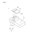
- FIGS. 1 show a terminal box according to an embodiment of the present invention, with FIG. 1(a) being a schematic cross-sectional view and FIG. 1(b) being a plan view.
- FIG. 2 is a perspective view of the terminal box from which a terminal panel portion has been separated.
- the terminal box is attached to each of the upstanding terminal portion 122a of the positive electrode current collecting portion 20 and the upstanding terminal portion 123a of the negative electrode current collecting portion 21, but the attachment structure is the same, and thus the present embodiment will be described in the context of the terminal box being attached to the upstanding terminal portion 122a of the positive electrode current collecting portion 20.
- a terminal box 1 includes a box case 11 that is placed on and fixed to the back film 125 of the solar cell string 116 in order to electrically connect the upstanding terminal portion (hereinafter also referred to as "output lead wire") 122a drawn from the back face of the solar cell string 116 through the back film 125 and a terminal panel 20 that is formed on the box case 11.
- the box case 11 includes a case main body 12 that is placed on and fixed to the back film 125 of the solar cell string 116 and a terminal panel fixing portion 13 for placing and fixing the terminal panel 20 above the case main body 12.
- the box case 11 is formed to have a rectangular parallelepiped shape that is long in the sideways direction in FIG. 1(b) and short in the width direction, and the terminal panel fixing portion 13 is formed to have a substantially cubic shape as a whole.
- an opening 14 (14a, 14b, 20a) for passing the output lead wire 122a through the terminal panel 20 is formed continuously from the bottom face of the case main body 11 to the top face of the terminal panel 20.
- the present embodiment does not employ a configuration as in the conventional technique 1 in which a main body through hole 104 and a terminal panel through hole 112 are provided separately. Consequently, wasted space as in the terminal box of the conventional technique 1 can be eliminated, reducing the size of the terminal box itself.
- the opening 14a formed in the terminal panel fixing portion 13 is formed by a pair of terminal panel fixing pieces 13a and 13b that are provided upright with a predetermined spacing therebetween in the lateral direction of the case main body 11, and the space between the terminal panel fixing pieces 13a and 13b serves as the opening 14a for passing the output lead wire 122a.
- the opening 14a formed in the terminal panel fixing portion 3 has a groove-like structure in which two sides are open, rather than a cylindrical hole.
- the potting material can easily flow from the opening 14a into the opening 14b provided in the case main body 11 (and to the back film 125 of the solar cell string 116), and it is thereby possible to reliably resin-seal the periphery of the output lead wire 122a drawn from the back film 125 of the solar cell string 116.
- the opening 20a of the terminal panel 20 is also formed to have a rectangular shape that is long in the width direction so as to conform to the above-described shape of the opening 14a.
- the opening 14b formed in the case main body 11 is formed to have a quadrilateral shape as viewed from above, and the inner wall face is formed to have a tapered shape that gradually becomes wider from the side communicating with the terminal panel fixing portion 13 (in other words, the lower edge of the opening 14a) toward the bottom face of the case main body 11.
- the opening 14b By forming the opening 14b to have such a tapered shape, the opening diameter of the lower end of the opening 14b for passing the output lead wire 122a becomes large, and it is therefore possible to prevent drawbacks such as the output lead wire 122a coming into contact with the edge of the opening 14b and thus being bent when the terminal box 1 is placed from above.
- the terminal panel 20 is formed to have a quadrilateral shape so as to conform to the shape of the top face of the terminal panel fixing portion 13, but one edge 20b is provided so as to protrude from the terminal panel fixing portion 13 so that a tip 122a1 of the output lead wire 122a can be bent and latched on.
- the tip 122a1 of the output lead wire 122a can be latched on and fixed to the terminal panel 20 by bending the output lead wire 122a protruding above from the opening 20a of the terminal panel 20 toward one edge of the terminal panel 20 (toward the right in FIG.
- the tip 122a1 of the output lead wire 122a can be reliably latched on and fixed to the terminal panel 20. Consequently, the next step of soldering the bent portions of the output lead wire 122a to the terminal panel 20 can be performed in a stable manner, and it is therefore possible to achieve a terminal box attachment structure that is sufficiently in compliance with the IEC standards.
- this eliminates the need for a space for routing the output lead wire in order to perform soldering as in the conventional technique, and thus provides an advantage of enhancing the degree of freedom of arrangement of diodes, other wires and the like that are provided in the terminal box.
- an air escape vent 16 extending from the bottom face to the top face of the case main body 11 may be provided at an appropriate location of the case main body 11. It should be noted, however, that the air vent 16 is provided at a position sufficiently away from the terminal panel fixing portion 13.
- an adhesive silicon resin 18 is applied to the bottom face of the case main body 12 of the terminal box 1 at the periphery thereof (it may be applied around the entire periphery or may be applied to four corners, for example).
- the air escape vent 16 the air present within the opening 14 and in the gap S between the back film 125 of the solar cell string 116 and the bottom face of the case main body 12 of the terminal box 1 can escape to the outside through the air escape vent 16 when the potting material flows into the opening 14, and it is therefore possible to reliably fill the potting material into the opening 14 (more specifically, to the back film 125 of the solar cell string 116 within the opening 14, and to the gap S between the back film 125 of the solar cell string 116 and the bottom face of the case main body 12 of the terminal box 1), as a result of which resin-sealing without creating holes can be performed.
- a method can be used in which a connection end of the external output line is secured directly to the other end of the terminal panel 20 by means of a rivet or the like.
- a solar cell module is produced by attaching the terminal box 1 onto the back film 125 of the solar cell string 116, electrically connecting the output lead wire 122a to the terminal panel 20, and electrically connecting an external output line to the terminal panel 20.
Landscapes
- Photovoltaic Devices (AREA)
Abstract
Description
- The present invention relates to a terminal box that electrically connects output lead wires that are connected to electrodes of solar cells and that are drawn through a back film of the solar cells, and more specifically, to a terminal box characterized by output lead wires connecting structure, and solar cells module including such a terminal box.
- Solar power generation systems for generating solar power in which a plurality of solar cell strings are placed in a matrix on the roof of buildings or the like are beginning to come into wide use. In such solar cells power generation system, each solar cell module is provided with a terminal box that can make an electrical connection with another solar cell module placed adjacent to the solar cell module.
- An example of a conventional terminal box is shown in
FIGS. 5 as aconventional technique 1.FIG. 5(a) is a cross-sectional view, andFIG. 5(b) is a plan view. - A
terminal box 200 according to theconventional technique 1 includes abox case 201 that is placed on and fixed to the back face of thesolar cell string 300 in order to electrically connect anoutput lead wire 301 drawn through aback film 310 of asolar cell string 300 and aterminal panel 210 that is formed on thebox case 201. Thebox case 201 includes a casemain body 202 that is placed on and fixed to the back face of thesolar cell string 300 and a terminalpanel fixing portion 203 for placing and fixing theterminal panel 210 above the casemain body 202. - In the case
main body 202, a main body throughhole 204 for drawing upward theoutput lead wire 301 drawn from the back face of thesolar cell string 300 is formed. Oneend 211 of theterminal panel 210 facing the main body throughhole 204 is provided so as to protrude from the terminalpanel fixing portion 203, and a terminal panel throughhole 212 for passing atip 302 of theoutput lead wire 301 is formed in this protruding portion. - When electrically connecting the
output lead wire 301 by using theterminal box 200 configured as described above, firstly, thesolar cell string 300 is placed on a workbench (not shown) with its back face facing upward, positioning is performed such that the main body throughhole 204 of the terminal box faces thetip 302 of theoutput lead wire 301 drawn upward from the back face of thesolar cell string 300, and theterminal box 200 is placed from above on thesolar cell string 300. Next, in this state, theoutput lead wire 301 protruding upward from the main body throughhole 204 is held with tweezers or the like and bent toward theterminal panel 210, and then thetip 302 of theoutput lead wire 301 is passed through the terminal panel throughhole 212 formed in theterminal panel 210 from above. Then, in this state, theoutput lead wire 301 on theterminal panel 210 is fixed to theterminal panel 210 by soldering, and thereby theoutput lead wire 301 is attached and fixed to theterminal panel 210. - The reason that the
tip 302 of theoutput lead wire 301 is passed through (latched on) the terminal panel throughhole 212 and then fixed by soldering rather than simply fixing the output lead wire by soldering is because it is defined as such by IEC (International Electro Technical Commission) standards which define that simply fixing a wire by soldering will not suffice. - As another example of a conventional terminal box, the structure of a terminal box (connection box) disclosed in
Patent Document 1 is shown inFIG. 6 . - A
terminal box 402 disclosed inPatent Document 1 has a structure in which the tip of alead frame 416 inserted from aframe insertion hole 426 is connected, by soldering, to the other longitudinal end of aterminal 421 that is inserted from a cable throughhole 410 of a boxmain body 424 and that is latched on aterminal fixing portion 427 so as to not come out, and the lower face of the boxmain body 424 of theterminal box 402 is adhesively fixed to the back face of a solar cell stringmain body 401 with an adhesive. - On the other hand, in the terminal box 100 of the
conventional technique 1 described above, theoutput lead wire 201 and the terminal panel 110 are fixed by soldering, but a terminal box configured to eliminate such a soldering step has been proposed (see, for example, Patent Document 2). - As shown in
FIG. 7 , a terminal box disclosed in Patent Document 2 is attached so as to cover an electrode lead-outportion 506 of asolar cell string 507, and an internal leadwire insertion hole 508 for inserting aninternal lead wire 503 is formed in the bottom face of theterminal box 501. Inside theterminal box 501, arelay terminal support 505 for mechanically fixing arelay terminal 504 is formed near the internal leadwire insertion hole 508. Theinternal lead wire 503 and anexternal output line 502 are electrically and mechanically connected to each other by therelay terminal 504, and therelay terminal 504 is mechanically fixed to therelay terminal support 505 with the stick-shapedrelay terminal support 505 passing through a locking portion (opening) 513 formed in therelay terminal 504. -
- [Patent Document 1]
JP 2001-250974A - [Patent Document 2]
JP H11-17204A - The terminal box of the
conventional technique 1 described above is problematic in that it requires a step of passing, from above, thetip 302 of theoutput lead wire 301, which protrudes upward from the main body throughhole 204, through the terminal panel throughhole 212 formed in theterminal panel 210, and thus automation is difficult to achieve. - In addition, the main body through
hole 204 through which theoutput lead wire 301 is drawn and the terminal panel throughhole 212 formed in theterminal panel 210 for passing thetip 302 of the drawnoutput lead wire 301 are separately provided, and theoutput lead wire 301 drawn from the main body throughhole 204 is bent and passed through the terminal panel throughhole 212. For this reason, there is a problem in that a certain distance is needed from the main body throughhole 204 to the terminal panel throughhole 212, and the space corresponding to this portion is wasteful. In other words, the problem is that it is difficult to achieve size reduction of the terminal box. This problem may also occur in the terminal boxes disclosed inPatent Documents 1 and 2 described above. - Furthermore, there is a certain distance between the main body through
hole 204 and the terminal panel throughhole 212, and therefore theoutput lead wire 301 needs to be drawn upward to a sufficient length from the main body throughhole 204. This poses a problem in that the drawnoutput lead wire 301 becomes unstable, raising a possibility that soldering of theoutput lead wire 301 to theterminal panel 210 might not be performed in a stable manner. This problem may also occur in the terminal box disclosed inPatent Document 1 described above. - Moreover, the inner diameter of the main body through
hole 204 needs to be sufficiently large in order to prevent theoutput lead wire 301 from coming into contact with the edge of the main body throughhole 204 of theterminal box 200 and being bent when theterminal box 200 is placed from above on thesolar cell string 300. In other words, it is necessary to form the main body throughhole 204 as a large opening. This raises a possibility that when passing, from above, thetip 302 of theoutput lead wire 301 through the terminal panel throughhole 212 of theterminal panel 210, if theoutput lead wire 301 is inserted deeply, thetip 302 of theoutput lead wire 301 might come into contact with aside face 203a of the terminalpanel fixing portion 203, atop face 202a of the casemain body 202 or the like, and thus might be curved into a C shape and run through the main body throughhole 204 into the back face of thesolar cell string 300. In this case, a problem of low dielectric strength arises. - The terminal box disclosed in
Patent Document 1 described above is also problematic in that thelead frame 416 is only soldered onto theterminal 421, and thus the fixing strength is insufficient, and that this method is not in compliance with the IEC standards. Likewise, the terminal box disclosed in Patent Document 2 also has problems in that theinternal lead wire 503 and theexternal output line 502 are fixed to therelay terminal 504 only by soldering, and thus the strength of the soldered portions is insufficient, and that this method is not in compliance with the IEC standards. - The present invention has been conceived to solve the above problems, and it is an object of the present invention to provide a terminal box that has solved the above problems by focusing particular attention on the terminal box of the
conventional technique 1 and improving it, and a solar cell module including such a terminal box. - In order to solve the above problems, the present invention provides a terminal box that electrically connects output lead wires that are connected to electrodes of solar cells and that are drawn through a back film of the solar cells, the terminal box including: a box case that is placed on and fixed to the back film; and a terminal panel that is formed on the box case and that electrically connects the output lead wires, the box case including a case main body that is placed on and fixed to the back film and a terminal panel fixing portion for placing and fixing the terminal panel above the case main body, wherein an opening for passing the output lead wire through the terminal panel is formed continuously from a bottom face of the case main body to a top face of the terminal panel.
- The present invention also provides solar cells module including a terminal box that electrically connects output lead wires that are connected to electrodes of solar cells and that are drawn through a back film of the solar cells, the terminal box including: a box case that is placed on and fixed to the back film; and a terminal panel that is formed on the box case and that electrically connects the output lead wires, the box case including a case main body that is placed on and fixed to the back film and a terminal panel fixing portion for placing and fixing the terminal panel above the case main body, wherein an opening for passing the output lead wire through the terminal panel is formed continuously from a bottom face of the case main body to a top face of the terminal panel.
- According to the above configurations, an opening for passing the output lead wire through the terminal panel is formed continuously from the bottom face of the case main body to the top face of the terminal panel. In other words, there is only one opening, and the present invention does not employ a configuration as in the
conventional technique 1 in which a main body through hole 104 and a terminal panel through hole 112 are provided separately. Consequently, wasted space as in the terminal box of theconventional technique 1 can be eliminated, reducing the size of the terminal box itself. - Furthermore, according to the present invention, it is preferable that the opening formed in the case main body includes a through hole having a tapered shape that gradually becomes wider from a side communicating with the terminal panel fixing portion toward the bottom face of the case main body. By forming the opening to have such a tapered shape, the opening diameter of the lower end of the opening for passing the output lead wire becomes large, and it is therefore possible to prevent drawbacks such as the output lead wire coming into contact with the edge of the opening and thus being bent.
- Furthermore, according to the present invention, it is possible to employ a configuration in which one edge of the terminal panel is provided so as to protrude from the terminal panel fixing portion such that a tip of the output lead wire can be bent and latched on. In other words, in the present invention, the tip of the output lead wire can be latched on and fixed to the terminal panel by bending the output lead wire protruding above from the opening toward one edge of the terminal panel so as to press it against the edge of the opening and bending the tip of the bent output lead wire downward and backward so as to press it against the edge of the terminal panel. That is to say, by bending the output lead wire only twice at two bending points, namely, the edge of the opening of the terminal panel and one edge of the terminal panel, the tip of the output lead wire can be reliably latched on fixed to the terminal panel. Consequently, the next step of soldering the tip of the output lead wire to the terminal panel can be performed in a stable manner, and it is therefore possible to achieve a terminal box attachment structure that is sufficiently in compliance with the IEC standards.
- Furthermore, according to the present invention, the terminal panel fixing portion may be formed by a pair of terminal panel fixing pieces that are provided upright with a predetermined spacing therebetween in a lateral direction of the case main body, and a space between the terminal panel fixing pieces may serve as the opening for passing the output lead wire. In other words, the opening formed in the terminal panel fixing portion has a groove-like structure in which two sides are open, rather than a cylindrical hole. Accordingly, when resin-sealing the terminal box by potting after the output lead wire and an external output line have been connected to the terminal box, the potting material can easily flow from the opening into the inside, and it is thereby possible to reliably resin-seal the periphery of the output lead wire drawn through the back film. In this case, it is possible to employ a configuration in which the case main body is provided with an air escape vent extending from the bottom face to a top face of the case main body. By providing the air escape vent, the air present within the opening and in the gap between the back face of the solar cell and the bottom face of the terminal box can escape to the outside through the air escape vent when the potting material flows into the opening, and it is therefore possible to reliably fill the potting material into the opening (more specifically, to the back film of the solar cell within the opening, and to the gap between the back film of the solar cell and the bottom face of the terminal box), as a result of which resin-sealing without creating holes can be performed.
- According to the present invention, an opening for passing the output lead wire through the terminal panel is formed continuously from the bottom face of the case main body to the top face of the terminal panel, and thus it is unnecessary to separately provide two through holes as in the conventional technique. Consequently, wasted space as in the terminal box of the conventional technique can be eliminated, reducing the size of the terminal box itself.
-
- [
FIGS. 1] FIGS. 1 show a terminal box according to an embodiment of the present invention, withFIG. 1(a) being a cross-sectional view andFIG. 1(b) being a plan view. - [
FIG. 2] FIG. 2 is a perspective view of the terminal box according to the embodiment. - [
FIGS. 3] FIGS. 3 show an example of a configuration of a solar cell string, withFIGS. 3(a) and 3(b) showing two scenes of a manufacturing process thereof. - [
FIG. 4] FIG. 4 is an explanatory diagram showing a step of laminating and sealing the solar cell string. - [
FIGS. 5] FIGS. 5 show a structure of a terminal box according to aconventional technique 1, withFIG. 5(a) being a cross-sectional view andFIG. 5(b) being a plan view. - [
FIG. 6] FIG. 6 is a cross-sectional view showing a structure of a terminal box (connection box) disclosed inPatent Document 1. - [
FIG. 7] FIG. 7 is an overall perspective view showing a structure of a terminal box (connection box) disclosed in Patent Document 2. - Hereinafter, an embodiment of the present invention will be described with reference to the drawings.
- Firstly, an example of a configuration of a solar cell string to which a terminal box according to the present invention is applied will be described with reference to
FIGS. 3(a), 3(b) and4 . -
Solar cells 115 are each formed by laminating, although not shown in the drawings, a transparent electrode film made of a transparent conductive film, a photoelectric conversion layer and a back face electrode film in this order on a light-transmittinginsulating substrate 111. The light-transmitting insulating substrate can be made of glass or a heat-resistant resin such as polyimide. The transparent electrode film can be made of Sn02, ZnO, ITO or the like. The photoelectric conversion layer can be made of amorphous silicon, microcrystalline silicon or the like. - Each
solar cell 115 thus configured has, as shown inFIG. 3(a) , a long strip shape with a length extending substantially across the entire width of the light-transmittinginsulating substrate 111. Asolar cell string 116 in which a plurality ofsolar cells 115 are connected in series is configured by connecting the transparent electrode film of one of each two adjacentsolar cells 115 and the back face electrode film of the other solar cell to each other. - On an end of the transparent electrode film of the
solar cell 115 located at one end of thesolar cell string 116, a P-typeelectrode terminal portion 117 having a linear shape with substantially the same length as thesolar cell 115 is formed, and on an end of the back face electrode film of thesolar cell 115 located at the other end of thesolar cell string 116, an N-typeelectrode terminal portion 118 having a linear shape with substantially the same length as thesolar cell 115 is formed. The P-typeelectrode terminal portion 117 and the N-typeelectrode terminal portion 118 serve as electrode lead-out portions. By forming these electrode terminal portions to have the same length as thesolar cell 115 as described above, a current flowing through thesolar cells 115 of thesolar cell string 116 in series can be extracted uniformly without local concentration of the current, and it is therefore possible to suppress the occurrence of series resistance losses. - An insulating
film 119 is placed on thesolar cell string 116 so as to extend between a center area of the P-typeelectrode terminal portion 117 and a center area of the N-typeelectrode terminal portion 118. The insulatingfilm 119 is placed such that it does not overlap the P-typeelectrode terminal portion 117 and the N-typeelectrode terminal portion 118. The insulatingfilm 119 is preferably a thermoplastic polymer film, and in particular, it is optimal to use a film made of EVA (ethylene vinyl acetate resin). - On the other hand, a positive electrode
current collecting portion 120 called "bus bar" and made of a copper foil having the same shape and size as the P-typeelectrode terminal portion 117 is electrically and mechanically bonded to the entire face of the P-typeelectrode terminal portion 117. Likewise, a negative electrodecurrent collecting portion 121 having the same shape and size as the N-typeelectrode terminal portion 118 is electrically and mechanically bonded to the entire face of the N-typeelectrode terminal portion 118. As a means of bonding these, soldering or a conductive paste can be used, for example. - A positive
electrode lead wire 122 and a negativeelectrode lead wire 123 that are made of flat cables are disposed in line (or parallel, i.e., disposed offset in the width direction) on the insulatingfilm 119, with their tips facing each other. - One end of the positive
electrode lead wire 122 is connected to a center position of the positive electrodecurrent collecting portion 120. The other end of the positiveelectrode lead wire 122 is located in a substantially center area of thesolar cell string 116, and is bent vertically with respect to the face of thesolar cell string 116 to serve as anupstanding terminal portion 122a. Likewise, one end of the negativeelectrode lead wire 123 is connected to a center position of the negative electrodecurrent collecting portion 121. The other end of the negativeelectrode lead wire 123 is located in a substantially center area of thesolar cell string 116, and is bent vertically with respect to the face of thesolar cell string 116 to serve as anupstanding terminal portion 123a. - The positive
electrode lead wire 122 and the negativeelectrode lead wire 123 are made of the same material (namely, a copper foil) as that of the positive electrode current collectingportion 20 and the negative electrode current collecting portion 21, and as a means of bonding the lead wires and the current collecting portions, soldering or spot welding can be used, for example. Although the positiveelectrode lead wire 122 and the negativeelectrode lead wire 123 extend across a plurality ofsolar cells 115, the insulatingfilm 119 is present between the lead wires and thesolar cells 115, and therefore thesolar cells 115 will not be short-circuited. It is desirable that the width of the insulatingfilm 119 is sufficiently larger than the width of the positiveelectrode lead wire 122 and the negativeelectrode lead wire 123, and the insulatingfilm 119 is disposed in the form of a belt-like sheet extending from the positive electrodecurrent collecting portion 120 to the negative electrodecurrent collecting portion 121. - In this state, as shown in
FIG. 4 , a sealing insulatingfilm 124 and aback film 125 serving as a back face protection material for weather resistance and high insulation are laminated and sealed on the entire face of thesolar cell string 116, with theupstanding terminal portions electrode lead wire 122 and the negativeelectrode lead wire 123 passing through through holes 124a and throughholes 125a. The sealing insulatingfilm 124 is preferably a thermoplastic polymer film made of the same material as that of the insulatingfilm 119, and in particular, it is optimal to use a film made of EVA (ethylene vinyl acetate resin). When the sealing insulatingfilm 124 is a thermoplastic polymer film made of the same material as that of the insulatingfilm 119, molecular bonding between the sealing insulatingfilm 124 and the insulatingfilm 119 proceeds effectively during thermal fusion in the laminating/sealing process, forming a complete one piece after cooling, and it is thereby possible to improve the water resistance of the solar cell string. Theback film 125 preferably has a three-layer structure of PET/Al/PET (PET: polyethylene terephthalate). As for the thicknesses of these films, for example, when the insulatingfilm 119 has a thickness of 100 µm and the sealing insulatingfilm 124 has a thickness of 600 µm, theback film 125 has a thickness of 100 µm. - In the
solar cell string 116 thus configured, a terminal box according to the present invention is attached and electrically connected to theupstanding terminal portions electrode lead wire 122 and the negativeelectrode lead wire 123 protruding upward from the throughholes 125a of theback film 125, an external output line is electrically attached to the terminal box, and thereby a solar cell module is produced. - The electrode arrangement in the
solar cell string 116 is merely exemplary, and the arrangement is not limited thereto. For example, the positiveelectrode lead wire 122 and the negativeelectrode lead wire 123 may be disposed at a position toward one of the ends of thesolar cell string 116, rather than the center area of thesolar cell string 116, and the lead wires may not need to be drawn to the center area. In other words, the positiveelectrode lead wire 122 and the negativeelectrode lead wire 123 may be disposed such that theupstanding terminal portions portion 20 and the negative electrode current collecting portion 21, respectively. -
FIGS. 1 show a terminal box according to an embodiment of the present invention, withFIG. 1(a) being a schematic cross-sectional view andFIG. 1(b) being a plan view.FIG. 2 is a perspective view of the terminal box from which a terminal panel portion has been separated. The terminal box is attached to each of theupstanding terminal portion 122a of the positive electrode current collectingportion 20 and theupstanding terminal portion 123a of the negative electrode current collecting portion 21, but the attachment structure is the same, and thus the present embodiment will be described in the context of the terminal box being attached to theupstanding terminal portion 122a of the positive electrode current collectingportion 20. - A
terminal box 1 according to the present embodiment includes abox case 11 that is placed on and fixed to theback film 125 of thesolar cell string 116 in order to electrically connect the upstanding terminal portion (hereinafter also referred to as "output lead wire") 122a drawn from the back face of thesolar cell string 116 through theback film 125 and aterminal panel 20 that is formed on thebox case 11. Thebox case 11 includes a casemain body 12 that is placed on and fixed to theback film 125 of thesolar cell string 116 and a terminalpanel fixing portion 13 for placing and fixing theterminal panel 20 above the casemain body 12. - In the present embodiment, the
box case 11 is formed to have a rectangular parallelepiped shape that is long in the sideways direction inFIG. 1(b) and short in the width direction, and the terminalpanel fixing portion 13 is formed to have a substantially cubic shape as a whole. - In such a configuration of the
box case 11, in the present embodiment, an opening 14 (14a, 14b, 20a) for passing theoutput lead wire 122a through theterminal panel 20 is formed continuously from the bottom face of the casemain body 11 to the top face of theterminal panel 20. In other words, there is only one opening for passing theoutput lead wire 122a, and the present embodiment does not employ a configuration as in theconventional technique 1 in which a main body through hole 104 and a terminal panel through hole 112 are provided separately. Consequently, wasted space as in the terminal box of theconventional technique 1 can be eliminated, reducing the size of the terminal box itself. - In the present embodiment, as shown in
FIG. 2 , theopening 14a formed in the terminalpanel fixing portion 13 is formed by a pair of terminalpanel fixing pieces main body 11, and the space between the terminalpanel fixing pieces opening 14a for passing theoutput lead wire 122a. In other words, theopening 14a formed in the terminal panel fixing portion 3 has a groove-like structure in which two sides are open, rather than a cylindrical hole. Accordingly, when resin-sealing theterminal box 1 by potting after theoutput lead wire 122a and an external output line (not shown) for connecting another solar cell module disposed adjacent thereto have been connected to theterminal box 1, the potting material can easily flow from theopening 14a into theopening 14b provided in the case main body 11 (and to theback film 125 of the solar cell string 116), and it is thereby possible to reliably resin-seal the periphery of theoutput lead wire 122a drawn from theback film 125 of thesolar cell string 116. - The
opening 20a of theterminal panel 20 is also formed to have a rectangular shape that is long in the width direction so as to conform to the above-described shape of theopening 14a. - Also, in the present embodiment, the
opening 14b formed in the casemain body 11 is formed to have a quadrilateral shape as viewed from above, and the inner wall face is formed to have a tapered shape that gradually becomes wider from the side communicating with the terminal panel fixing portion 13 (in other words, the lower edge of theopening 14a) toward the bottom face of the casemain body 11. By forming theopening 14b to have such a tapered shape, the opening diameter of the lower end of theopening 14b for passing theoutput lead wire 122a becomes large, and it is therefore possible to prevent drawbacks such as theoutput lead wire 122a coming into contact with the edge of theopening 14b and thus being bent when theterminal box 1 is placed from above. - Also, in the present embodiment, the
terminal panel 20 is formed to have a quadrilateral shape so as to conform to the shape of the top face of the terminalpanel fixing portion 13, but oneedge 20b is provided so as to protrude from the terminalpanel fixing portion 13 so that a tip 122a1 of theoutput lead wire 122a can be bent and latched on. In other words, in the present embodiment, the tip 122a1 of theoutput lead wire 122a can be latched on and fixed to theterminal panel 20 by bending theoutput lead wire 122a protruding above from theopening 20a of theterminal panel 20 toward one edge of the terminal panel 20 (toward the right inFIG. 1 ) so as to pres it against the edge of theopening 20a and bending the tip of the bent output lead wire downward and backward so as to press it against theedge 20b of theterminal panel 20. That is to say, by bending theoutput lead wire 122a only twice at two bending points, namely, the edge of theopening 20a of theterminal panel 20 and oneedge 20b of theterminal panel 20, the tip 122a1 of theoutput lead wire 122a can be reliably latched on and fixed to theterminal panel 20. Consequently, the next step of soldering the bent portions of theoutput lead wire 122a to theterminal panel 20 can be performed in a stable manner, and it is therefore possible to achieve a terminal box attachment structure that is sufficiently in compliance with the IEC standards. In addition, this eliminates the need for a space for routing the output lead wire in order to perform soldering as in the conventional technique, and thus provides an advantage of enhancing the degree of freedom of arrangement of diodes, other wires and the like that are provided in the terminal box. - Also, in the present embodiment, an
air escape vent 16 extending from the bottom face to the top face of the casemain body 11 may be provided at an appropriate location of the casemain body 11. It should be noted, however, that theair vent 16 is provided at a position sufficiently away from the terminalpanel fixing portion 13. In order to attach theterminal box 1 onto theback film 125 of thesolar cell string 116, anadhesive silicon resin 18 is applied to the bottom face of the casemain body 12 of theterminal box 1 at the periphery thereof (it may be applied around the entire periphery or may be applied to four corners, for example). Thus, when theterminal box 1 is adhesively fixed onto theback film 125 of thesolar cell string 116, a gap S corresponding to the thickness of thesilicon resin 18 is created between the bottom face of the casemain body 12 and theback film 125 of thesolar cell string 116. Accordingly, by providing theair escape vent 16, the air present within the opening 14 and in the gap S between theback film 125 of thesolar cell string 116 and the bottom face of the casemain body 12 of theterminal box 1 can escape to the outside through theair escape vent 16 when the potting material flows into the opening 14, and it is therefore possible to reliably fill the potting material into the opening 14 (more specifically, to theback film 125 of thesolar cell string 116 within the opening 14, and to the gap S between theback film 125 of thesolar cell string 116 and the bottom face of the casemain body 12 of the terminal box 1), as a result of which resin-sealing without creating holes can be performed. - Although not shown in the drawings, as the method of fixing an external output line fixed onto the
terminal panel 20, a method can be used in which a connection end of the external output line is secured directly to the other end of theterminal panel 20 by means of a rivet or the like. As described above, a solar cell module is produced by attaching theterminal box 1 onto theback film 125 of thesolar cell string 116, electrically connecting theoutput lead wire 122a to theterminal panel 20, and electrically connecting an external output line to theterminal panel 20. - The present invention may be embodied in various other forms without departing from the gist or essential characteristics thereof. Therefore, the embodiment given above is to be considered in all respects as illustrative and not limiting. The scope of the invention is indicated by the appended claims rather than by the foregoing description, and all modifications or changes that come within the meaning and range of equivalency of the claims are intended to be embraced therein.
-
- 1
- Terminal Box
- 11
- Box Case
- 12
- Case Main Body
- 13
- Terminal Panel Fixing Portion
- 13a, 13b
- Terminal Panel Fixing Piece
- 14 (14a, 14b, 20a)
- Opening
- 16
- Air Escape Vent
- 20
- Terminal Panel
- 20b
- One Edge
- 111
- Light-Transmitting Insulating Substrate
- 115
- Solar Cell
- 116
- Solar Cell String (Thin Film Solar Cell String)
- 117
- P-Type Electrode Terminal Portion
- 118
- N-Type Electrode Terminal Portion
- 119
- Insulating Film
- 120
- Positive Electrode Current Collecting Portion
- 121
- Negative Electrode Current Collecting Portion
- 122
- Positive Electrode Lead Wire
- 123
- Negative Electrode Lead Wire
- 122a, 123a
- Upstanding Terminal Portion
- 122a1
- Tip
- 124
- Sealing Insulating Film
- 125
- Back Film
- 124a, 125a
- Through Hole
Claims (6)
- A terminal box that electrically connects output lead wires that are connected to electrodes of solar cells and that are drawn through a back film of the solar cells,
the terminal box comprising:a box case that is placed on and fixed to the back film; anda terminal panel that is formed on the box case and that electrically connects the output lead wires, the box case comprising a case main body that is placed on and fixed to the back film and a terminal panel fixing portion for placing and fixing the terminal panel above the case main body,wherein an opening for passing the output lead wire through the terminal panel is formed continuously from a bottom face of the case main body to a top face of the terminal panel. - The terminal box according to claim 1,
wherein the opening formed in the case main body comprises a through hole having a tapered shape that gradually becomes wider from a side communicating with the terminal panel fixing portion toward the bottom face of the case main body. - The terminal box according to claim 1,
wherein one edge of the terminal panel is provided so as to protrude from the terminal panel fixing portion such that a tip of the output lead wire can be bent and latched on. - The terminal box according to claim 1,
wherein the terminal panel fixing portion is formed by a pair of terminal panel fixing pieces that are provided upright with a predetermined spacing therebetween in a lateral direction of the case main body, and a space between the terminal panel fixing pieces serves as the opening for passing the output lead wire. - The terminal box according to any one of claims 1 to 4,
wherein the case main body is provided with an air escape vent extending from the bottom face to a top face of the case main body. - A solar cell module comprising a terminal box that electrically connects output lead wires that are connected to electrodes of solar cells and that are drawn through a back film of the solar cells,
the terminal box comprising:a box case that is placed on and fixed to the back film; anda terminal panel that is formed on the box case and that electrically connects the output lead wires, the box case comprising a case main body that is placed on and fixed to the back film, and a terminal panel fixing portion for placing and fixing the terminal panel above the case main body,wherein an opening for passing the output lead wire through the terminal panel is formed continuously from a bottom face of the case main body to a top face of the terminal panel.
Applications Claiming Priority (2)
| Application Number | Priority Date | Filing Date | Title |
|---|---|---|---|
| JP2008147024A JP4384241B1 (en) | 2008-06-04 | 2008-06-04 | Terminal box and solar cell module |
| PCT/JP2009/060147 WO2009148078A1 (en) | 2008-06-04 | 2009-06-03 | Terminal box and solar cell module |
Publications (3)
| Publication Number | Publication Date |
|---|---|
| EP2296188A1 true EP2296188A1 (en) | 2011-03-16 |
| EP2296188A4 EP2296188A4 (en) | 2014-05-21 |
| EP2296188B1 EP2296188B1 (en) | 2018-11-07 |
Family
ID=41398151
Family Applications (1)
| Application Number | Title | Priority Date | Filing Date |
|---|---|---|---|
| EP09758345.4A Active EP2296188B1 (en) | 2008-06-04 | 2009-06-03 | Terminal box and solar cell module |
Country Status (4)
| Country | Link |
|---|---|
| US (1) | US8536466B2 (en) |
| EP (1) | EP2296188B1 (en) |
| JP (1) | JP4384241B1 (en) |
| WO (1) | WO2009148078A1 (en) |
Cited By (4)
| Publication number | Priority date | Publication date | Assignee | Title |
|---|---|---|---|---|
| GB2490499A (en) * | 2011-05-03 | 2012-11-07 | Solaredge Technologies Ltd | Junction box assembly for electrical connections to photovoltaic panels |
| US8476524B2 (en) | 2009-05-22 | 2013-07-02 | Solaredge Technologies Ltd. | Electrically isolated heat dissipating junction box |
| CN104143957A (en) * | 2013-05-09 | 2014-11-12 | 星电株式会社 | Terminal box |
| EP3588588A1 (en) * | 2018-06-29 | 2020-01-01 | Shandong Zibo Hanergy Thin Film Solar Cell Co., Ltd | Device for assisting a bus bar to pass through a hole and solar assembly production line |
Families Citing this family (14)
| Publication number | Priority date | Publication date | Assignee | Title |
|---|---|---|---|---|
| DE102008062034B4 (en) * | 2008-12-12 | 2010-08-12 | Tyco Electronics Amp Gmbh | Connecting device for connection to a solar module and solar module with such a connection device |
| US8513516B2 (en) * | 2010-08-27 | 2013-08-20 | Primestar Solar, Inc. | Intra-laminate disk layer for thin film photovoltaic devices and their methods of manufacture |
| WO2012114638A1 (en) * | 2011-02-25 | 2012-08-30 | シャープ株式会社 | Solar cell module, solar cell module manufacturing method, and terminal box used in solar cell module manufacture |
| JP5745349B2 (en) * | 2011-06-27 | 2015-07-08 | デクセリアルズ株式会社 | Manufacturing method of solar cell module |
| JP5729648B2 (en) * | 2011-10-13 | 2015-06-03 | ホシデン株式会社 | Terminal box for solar cell module |
| US8722136B2 (en) | 2011-10-21 | 2014-05-13 | First Solar, Inc. | Heat strengthening of a glass superstrate for thin film photovoltaic devices |
| KR101305624B1 (en) * | 2011-11-01 | 2013-09-09 | 엘지이노텍 주식회사 | Solar cell module and method of fabricating the same |
| JP2013098399A (en) * | 2011-11-02 | 2013-05-20 | Sharp Corp | Solar battery module, terminal structure, terminal structure coupling apparatus and manufacturing method of solar battery module |
| WO2013099559A1 (en) * | 2011-12-28 | 2013-07-04 | シャープ株式会社 | Terminal box, method for attaching lead wire to terminal box, and solar cell module |
| JP2013171860A (en) * | 2012-02-17 | 2013-09-02 | Mitsubishi Electric Corp | Terminal box |
| JP5902726B2 (en) * | 2014-01-15 | 2016-04-13 | トヨタ自動車株式会社 | Rotating electrical machine stator |
| JP6283278B2 (en) | 2014-07-18 | 2018-02-21 | ホシデン株式会社 | Connection method for terminal box and output line |
| US11127336B2 (en) * | 2015-09-23 | 2021-09-21 | Boe Technology Group Co., Ltd. | Gate on array (GOA) unit, gate driver circuit and display device |
| JP7063834B2 (en) * | 2019-03-13 | 2022-05-09 | 株式会社日立建機ティエラ | Electric construction machinery |
Family Cites Families (8)
| Publication number | Priority date | Publication date | Assignee | Title |
|---|---|---|---|---|
| AU608701B2 (en) | 1988-04-11 | 1991-04-11 | Ebara Solar, Inc. | Integral frame and junction box for a photovoltaic module |
| JP3459754B2 (en) | 1997-06-24 | 2003-10-27 | キヤノン株式会社 | Terminal box for solar cell module, method of connecting the same, and solar cell module |
| JP2001250974A (en) | 2000-03-07 | 2001-09-14 | Sumitomo Wiring Syst Ltd | Connection box device for solar battery module |
| DE10358140B4 (en) * | 2003-12-10 | 2006-01-05 | Günther Spelsberg GmbH & Co. KG | Electrical connection and connection box for a solar cell module |
| JP2005353734A (en) * | 2004-06-09 | 2005-12-22 | Sumitomo Wiring Syst Ltd | Terminal box for solar cell module |
| JP2006041262A (en) * | 2004-07-28 | 2006-02-09 | Sumitomo Wiring Syst Ltd | Terminal box for solar cell module |
| JP4699060B2 (en) | 2005-03-24 | 2011-06-08 | 三菱電機株式会社 | Terminal box device for solar cell module |
| JP4418397B2 (en) * | 2005-04-27 | 2010-02-17 | 行田電線株式会社 | Terminal box for solar cell module |
-
2008
- 2008-06-04 JP JP2008147024A patent/JP4384241B1/en active Active
-
2009
- 2009-06-03 EP EP09758345.4A patent/EP2296188B1/en active Active
- 2009-06-03 US US12/996,432 patent/US8536466B2/en not_active Expired - Fee Related
- 2009-06-03 WO PCT/JP2009/060147 patent/WO2009148078A1/en not_active Ceased
Cited By (9)
| Publication number | Priority date | Publication date | Assignee | Title |
|---|---|---|---|---|
| US8476524B2 (en) | 2009-05-22 | 2013-07-02 | Solaredge Technologies Ltd. | Electrically isolated heat dissipating junction box |
| US8895852B2 (en) | 2011-05-02 | 2014-11-25 | Solaredge Technologies Ltd. | Junction box for snap together electrical connections to photovoltaic panels |
| US9160092B2 (en) | 2011-05-02 | 2015-10-13 | Solaredge Technologies Ltd | Junction box for snap together electrical connections to photovoltaic panels |
| US11005417B2 (en) | 2011-05-02 | 2021-05-11 | Solaredge Technologies Ltd. | Junction box for snap together electrical connections to photovoltaic panels |
| GB2490499A (en) * | 2011-05-03 | 2012-11-07 | Solaredge Technologies Ltd | Junction box assembly for electrical connections to photovoltaic panels |
| CN104143957A (en) * | 2013-05-09 | 2014-11-12 | 星电株式会社 | Terminal box |
| EP2802016A1 (en) * | 2013-05-09 | 2014-11-12 | Hosiden Corporation | Terminal box |
| US9252571B2 (en) | 2013-05-09 | 2016-02-02 | Hosiden Corporation | Terminal box |
| EP3588588A1 (en) * | 2018-06-29 | 2020-01-01 | Shandong Zibo Hanergy Thin Film Solar Cell Co., Ltd | Device for assisting a bus bar to pass through a hole and solar assembly production line |
Also Published As
| Publication number | Publication date |
|---|---|
| EP2296188B1 (en) | 2018-11-07 |
| EP2296188A4 (en) | 2014-05-21 |
| JP2009295743A (en) | 2009-12-17 |
| US8536466B2 (en) | 2013-09-17 |
| US20110073362A1 (en) | 2011-03-31 |
| WO2009148078A1 (en) | 2009-12-10 |
| JP4384241B1 (en) | 2009-12-16 |
Similar Documents
| Publication | Publication Date | Title |
|---|---|---|
| EP2296188B1 (en) | Terminal box and solar cell module | |
| EP2296189A1 (en) | Solar cell module | |
| US8921684B2 (en) | Solar cell module and manufacturing method thereof | |
| US8952240B2 (en) | Solar cell module | |
| JP5031698B2 (en) | Solar cell module | |
| US8461450B2 (en) | Solar cell module and manufacturing method of solar cell module | |
| EP2043164A2 (en) | Solar cell module | |
| US20050133086A1 (en) | Solar cell module with conductor member and with bypass diode arranged on condcutor member, and method of producing same | |
| CN115411126A (en) | Photovoltaic modules | |
| US20110271998A1 (en) | Solar cell module and manufacturing method thereof | |
| JP2012019023A (en) | Solar cell module assembly and moving body equipped with the same | |
| JP2010283231A (en) | Solar cell module and manufacturing method thereof | |
| JP5306490B2 (en) | Terminal box and solar cell module | |
| JP5132646B2 (en) | Terminal box and solar cell module | |
| EP4307393A1 (en) | Method for manufacturing a solar cell module and solar cell module | |
| EP2228831A2 (en) | Solar cell module | |
| JP2002141535A (en) | Power lead-out method for solar cell module | |
| JP6042710B2 (en) | SOLAR CELL MODULE AND METHOD FOR MANUFACTURING SOLAR CELL MODULE | |
| JP2012142637A (en) | Solar cell module | |
| JP2012142634A (en) | Solar cell module and manufacturing method of the same | |
| JP2012142635A (en) | Solar cell module | |
| JP2012142633A (en) | Solar cell module and manufacturing method of the same | |
| JP2012142636A (en) | Solar cell module and manufacturing method of the same |
Legal Events
| Date | Code | Title | Description |
|---|---|---|---|
| PUAI | Public reference made under article 153(3) epc to a published international application that has entered the european phase |
Free format text: ORIGINAL CODE: 0009012 |
|
| 17P | Request for examination filed |
Effective date: 20101209 |
|
| AK | Designated contracting states |
Kind code of ref document: A1 Designated state(s): AT BE BG CH CY CZ DE DK EE ES FI FR GB GR HR HU IE IS IT LI LT LU LV MC MK MT NL NO PL PT RO SE SI SK TR |
|
| AX | Request for extension of the european patent |
Extension state: AL BA RS |
|
| DAX | Request for extension of the european patent (deleted) | ||
| A4 | Supplementary search report drawn up and despatched |
Effective date: 20140424 |
|
| RIC1 | Information provided on ipc code assigned before grant |
Ipc: H01L 31/02 20060101ALI20140416BHEP Ipc: H01L 31/048 20140101AFI20140416BHEP |
|
| REG | Reference to a national code |
Ref country code: DE Ref legal event code: R079 Ref document number: 602009055498 Country of ref document: DE Free format text: PREVIOUS MAIN CLASS: H01L0031040000 Ipc: H01L0031020000 |
|
| GRAP | Despatch of communication of intention to grant a patent |
Free format text: ORIGINAL CODE: EPIDOSNIGR1 |
|
| STAA | Information on the status of an ep patent application or granted ep patent |
Free format text: STATUS: GRANT OF PATENT IS INTENDED |
|
| RIC1 | Information provided on ipc code assigned before grant |
Ipc: H01L 31/02 20060101AFI20180516BHEP Ipc: H02S 40/34 20140101ALI20180516BHEP |
|
| INTG | Intention to grant announced |
Effective date: 20180611 |
|
| GRAS | Grant fee paid |
Free format text: ORIGINAL CODE: EPIDOSNIGR3 |
|
| GRAA | (expected) grant |
Free format text: ORIGINAL CODE: 0009210 |
|
| STAA | Information on the status of an ep patent application or granted ep patent |
Free format text: STATUS: THE PATENT HAS BEEN GRANTED |
|
| AK | Designated contracting states |
Kind code of ref document: B1 Designated state(s): AT BE BG CH CY CZ DE DK EE ES FI FR GB GR HR HU IE IS IT LI LT LU LV MC MK MT NL NO PL PT RO SE SI SK TR |
|
| REG | Reference to a national code |
Ref country code: GB Ref legal event code: FG4D |
|
| REG | Reference to a national code |
Ref country code: CH Ref legal event code: EP Ref country code: AT Ref legal event code: REF Ref document number: 1063111 Country of ref document: AT Kind code of ref document: T Effective date: 20181115 |
|
| REG | Reference to a national code |
Ref country code: IE Ref legal event code: FG4D |
|
| REG | Reference to a national code |
Ref country code: DE Ref legal event code: R096 Ref document number: 602009055498 Country of ref document: DE |
|
| REG | Reference to a national code |
Ref country code: NL Ref legal event code: MP Effective date: 20181107 |
|
| REG | Reference to a national code |
Ref country code: LT Ref legal event code: MG4D |
|
| REG | Reference to a national code |
Ref country code: AT Ref legal event code: MK05 Ref document number: 1063111 Country of ref document: AT Kind code of ref document: T Effective date: 20181107 |
|
| PG25 | Lapsed in a contracting state [announced via postgrant information from national office to epo] |
Ref country code: AT Free format text: LAPSE BECAUSE OF FAILURE TO SUBMIT A TRANSLATION OF THE DESCRIPTION OR TO PAY THE FEE WITHIN THE PRESCRIBED TIME-LIMIT Effective date: 20181107 Ref country code: HR Free format text: LAPSE BECAUSE OF FAILURE TO SUBMIT A TRANSLATION OF THE DESCRIPTION OR TO PAY THE FEE WITHIN THE PRESCRIBED TIME-LIMIT Effective date: 20181107 Ref country code: LT Free format text: LAPSE BECAUSE OF FAILURE TO SUBMIT A TRANSLATION OF THE DESCRIPTION OR TO PAY THE FEE WITHIN THE PRESCRIBED TIME-LIMIT Effective date: 20181107 Ref country code: ES Free format text: LAPSE BECAUSE OF FAILURE TO SUBMIT A TRANSLATION OF THE DESCRIPTION OR TO PAY THE FEE WITHIN THE PRESCRIBED TIME-LIMIT Effective date: 20181107 Ref country code: BG Free format text: LAPSE BECAUSE OF FAILURE TO SUBMIT A TRANSLATION OF THE DESCRIPTION OR TO PAY THE FEE WITHIN THE PRESCRIBED TIME-LIMIT Effective date: 20190207 Ref country code: LV Free format text: LAPSE BECAUSE OF FAILURE TO SUBMIT A TRANSLATION OF THE DESCRIPTION OR TO PAY THE FEE WITHIN THE PRESCRIBED TIME-LIMIT Effective date: 20181107 Ref country code: FI Free format text: LAPSE BECAUSE OF FAILURE TO SUBMIT A TRANSLATION OF THE DESCRIPTION OR TO PAY THE FEE WITHIN THE PRESCRIBED TIME-LIMIT Effective date: 20181107 Ref country code: IS Free format text: LAPSE BECAUSE OF FAILURE TO SUBMIT A TRANSLATION OF THE DESCRIPTION OR TO PAY THE FEE WITHIN THE PRESCRIBED TIME-LIMIT Effective date: 20190307 Ref country code: NO Free format text: LAPSE BECAUSE OF FAILURE TO SUBMIT A TRANSLATION OF THE DESCRIPTION OR TO PAY THE FEE WITHIN THE PRESCRIBED TIME-LIMIT Effective date: 20190207 |
|
| PG25 | Lapsed in a contracting state [announced via postgrant information from national office to epo] |
Ref country code: NL Free format text: LAPSE BECAUSE OF FAILURE TO SUBMIT A TRANSLATION OF THE DESCRIPTION OR TO PAY THE FEE WITHIN THE PRESCRIBED TIME-LIMIT Effective date: 20181107 Ref country code: GR Free format text: LAPSE BECAUSE OF FAILURE TO SUBMIT A TRANSLATION OF THE DESCRIPTION OR TO PAY THE FEE WITHIN THE PRESCRIBED TIME-LIMIT Effective date: 20190208 Ref country code: PT Free format text: LAPSE BECAUSE OF FAILURE TO SUBMIT A TRANSLATION OF THE DESCRIPTION OR TO PAY THE FEE WITHIN THE PRESCRIBED TIME-LIMIT Effective date: 20190307 Ref country code: SE Free format text: LAPSE BECAUSE OF FAILURE TO SUBMIT A TRANSLATION OF THE DESCRIPTION OR TO PAY THE FEE WITHIN THE PRESCRIBED TIME-LIMIT Effective date: 20181107 |
|
| PG25 | Lapsed in a contracting state [announced via postgrant information from national office to epo] |
Ref country code: DK Free format text: LAPSE BECAUSE OF FAILURE TO SUBMIT A TRANSLATION OF THE DESCRIPTION OR TO PAY THE FEE WITHIN THE PRESCRIBED TIME-LIMIT Effective date: 20181107 Ref country code: PL Free format text: LAPSE BECAUSE OF FAILURE TO SUBMIT A TRANSLATION OF THE DESCRIPTION OR TO PAY THE FEE WITHIN THE PRESCRIBED TIME-LIMIT Effective date: 20181107 Ref country code: IT Free format text: LAPSE BECAUSE OF FAILURE TO SUBMIT A TRANSLATION OF THE DESCRIPTION OR TO PAY THE FEE WITHIN THE PRESCRIBED TIME-LIMIT Effective date: 20181107 Ref country code: CZ Free format text: LAPSE BECAUSE OF FAILURE TO SUBMIT A TRANSLATION OF THE DESCRIPTION OR TO PAY THE FEE WITHIN THE PRESCRIBED TIME-LIMIT Effective date: 20181107 |
|
| REG | Reference to a national code |
Ref country code: DE Ref legal event code: R097 Ref document number: 602009055498 Country of ref document: DE |
|
| PG25 | Lapsed in a contracting state [announced via postgrant information from national office to epo] |
Ref country code: SK Free format text: LAPSE BECAUSE OF FAILURE TO SUBMIT A TRANSLATION OF THE DESCRIPTION OR TO PAY THE FEE WITHIN THE PRESCRIBED TIME-LIMIT Effective date: 20181107 Ref country code: EE Free format text: LAPSE BECAUSE OF FAILURE TO SUBMIT A TRANSLATION OF THE DESCRIPTION OR TO PAY THE FEE WITHIN THE PRESCRIBED TIME-LIMIT Effective date: 20181107 Ref country code: RO Free format text: LAPSE BECAUSE OF FAILURE TO SUBMIT A TRANSLATION OF THE DESCRIPTION OR TO PAY THE FEE WITHIN THE PRESCRIBED TIME-LIMIT Effective date: 20181107 |
|
| PLBE | No opposition filed within time limit |
Free format text: ORIGINAL CODE: 0009261 |
|
| STAA | Information on the status of an ep patent application or granted ep patent |
Free format text: STATUS: NO OPPOSITION FILED WITHIN TIME LIMIT |
|
| 26N | No opposition filed |
Effective date: 20190808 |
|
| PG25 | Lapsed in a contracting state [announced via postgrant information from national office to epo] |
Ref country code: SI Free format text: LAPSE BECAUSE OF FAILURE TO SUBMIT A TRANSLATION OF THE DESCRIPTION OR TO PAY THE FEE WITHIN THE PRESCRIBED TIME-LIMIT Effective date: 20181107 |
|
| PG25 | Lapsed in a contracting state [announced via postgrant information from national office to epo] |
Ref country code: MC Free format text: LAPSE BECAUSE OF FAILURE TO SUBMIT A TRANSLATION OF THE DESCRIPTION OR TO PAY THE FEE WITHIN THE PRESCRIBED TIME-LIMIT Effective date: 20181107 |
|
| REG | Reference to a national code |
Ref country code: CH Ref legal event code: PL |
|
| GBPC | Gb: european patent ceased through non-payment of renewal fee |
Effective date: 20190603 |
|
| REG | Reference to a national code |
Ref country code: BE Ref legal event code: MM Effective date: 20190630 |
|
| PG25 | Lapsed in a contracting state [announced via postgrant information from national office to epo] |
Ref country code: TR Free format text: LAPSE BECAUSE OF FAILURE TO SUBMIT A TRANSLATION OF THE DESCRIPTION OR TO PAY THE FEE WITHIN THE PRESCRIBED TIME-LIMIT Effective date: 20181107 |
|
| PG25 | Lapsed in a contracting state [announced via postgrant information from national office to epo] |
Ref country code: GB Free format text: LAPSE BECAUSE OF NON-PAYMENT OF DUE FEES Effective date: 20190603 Ref country code: IE Free format text: LAPSE BECAUSE OF NON-PAYMENT OF DUE FEES Effective date: 20190603 |
|
| PG25 | Lapsed in a contracting state [announced via postgrant information from national office to epo] |
Ref country code: CH Free format text: LAPSE BECAUSE OF NON-PAYMENT OF DUE FEES Effective date: 20190630 Ref country code: BE Free format text: LAPSE BECAUSE OF NON-PAYMENT OF DUE FEES Effective date: 20190630 Ref country code: LU Free format text: LAPSE BECAUSE OF NON-PAYMENT OF DUE FEES Effective date: 20190603 Ref country code: LI Free format text: LAPSE BECAUSE OF NON-PAYMENT OF DUE FEES Effective date: 20190630 |
|
| PG25 | Lapsed in a contracting state [announced via postgrant information from national office to epo] |
Ref country code: FR Free format text: LAPSE BECAUSE OF NON-PAYMENT OF DUE FEES Effective date: 20190630 |
|
| PG25 | Lapsed in a contracting state [announced via postgrant information from national office to epo] |
Ref country code: CY Free format text: LAPSE BECAUSE OF FAILURE TO SUBMIT A TRANSLATION OF THE DESCRIPTION OR TO PAY THE FEE WITHIN THE PRESCRIBED TIME-LIMIT Effective date: 20181107 |
|
| PG25 | Lapsed in a contracting state [announced via postgrant information from national office to epo] |
Ref country code: MT Free format text: LAPSE BECAUSE OF FAILURE TO SUBMIT A TRANSLATION OF THE DESCRIPTION OR TO PAY THE FEE WITHIN THE PRESCRIBED TIME-LIMIT Effective date: 20181107 Ref country code: HU Free format text: LAPSE BECAUSE OF FAILURE TO SUBMIT A TRANSLATION OF THE DESCRIPTION OR TO PAY THE FEE WITHIN THE PRESCRIBED TIME-LIMIT; INVALID AB INITIO Effective date: 20090603 |
|
| PG25 | Lapsed in a contracting state [announced via postgrant information from national office to epo] |
Ref country code: MK Free format text: LAPSE BECAUSE OF FAILURE TO SUBMIT A TRANSLATION OF THE DESCRIPTION OR TO PAY THE FEE WITHIN THE PRESCRIBED TIME-LIMIT Effective date: 20181107 |
|
| REG | Reference to a national code |
Ref country code: DE Ref legal event code: R079 Ref document number: 602009055498 Country of ref document: DE Free format text: PREVIOUS MAIN CLASS: H01L0031020000 Ipc: H10F0077000000 |
|
| PGFP | Annual fee paid to national office [announced via postgrant information from national office to epo] |
Ref country code: DE Payment date: 20250618 Year of fee payment: 17 |