EP2290937B1 - Method and apparatus for controlling shared positive protection - Google Patents
Method and apparatus for controlling shared positive protection Download PDFInfo
- Publication number
- EP2290937B1 EP2290937B1 EP10251469.2A EP10251469A EP2290937B1 EP 2290937 B1 EP2290937 B1 EP 2290937B1 EP 10251469 A EP10251469 A EP 10251469A EP 2290937 B1 EP2290937 B1 EP 2290937B1
- Authority
- EP
- European Patent Office
- Prior art keywords
- interface
- positive
- reference voltage
- coupled
- lines
- Prior art date
- Legal status (The legal status is an assumption and is not a legal conclusion. Google has not performed a legal analysis and makes no representation as to the accuracy of the status listed.)
- Active
Links
- 238000000034 method Methods 0.000 title claims description 7
- 230000001012 protector Effects 0.000 claims description 79
- 239000003990 capacitor Substances 0.000 claims description 11
- 238000002955 isolation Methods 0.000 claims description 8
- 238000012544 monitoring process Methods 0.000 claims description 2
- 238000010586 diagram Methods 0.000 description 7
- 230000001960 triggered effect Effects 0.000 description 4
- 230000008901 benefit Effects 0.000 description 3
- 239000004020 conductor Substances 0.000 description 3
- 238000013461 design Methods 0.000 description 3
- 230000005923 long-lasting effect Effects 0.000 description 3
- 208000035217 Ring chromosome 1 syndrome Diseases 0.000 description 2
- 230000000903 blocking effect Effects 0.000 description 2
- 230000006854 communication Effects 0.000 description 2
- 238000004891 communication Methods 0.000 description 2
- 238000011161 development Methods 0.000 description 2
- 230000000694 effects Effects 0.000 description 2
- 230000006870 function Effects 0.000 description 2
- 238000004519 manufacturing process Methods 0.000 description 2
- 238000012986 modification Methods 0.000 description 2
- 230000004048 modification Effects 0.000 description 2
- 230000009993 protective function Effects 0.000 description 2
- 230000009467 reduction Effects 0.000 description 2
- 230000004044 response Effects 0.000 description 2
- 230000002441 reversible effect Effects 0.000 description 2
- 238000012360 testing method Methods 0.000 description 2
- 230000001052 transient effect Effects 0.000 description 2
- 230000002159 abnormal effect Effects 0.000 description 1
- 230000003213 activating effect Effects 0.000 description 1
- 230000007175 bidirectional communication Effects 0.000 description 1
- 230000005540 biological transmission Effects 0.000 description 1
- 238000010276 construction Methods 0.000 description 1
- 230000008878 coupling Effects 0.000 description 1
- 238000010168 coupling process Methods 0.000 description 1
- 238000005859 coupling reaction Methods 0.000 description 1
- 238000001514 detection method Methods 0.000 description 1
- 230000009977 dual effect Effects 0.000 description 1
- 238000004146 energy storage Methods 0.000 description 1
- 230000007274 generation of a signal involved in cell-cell signaling Effects 0.000 description 1
- 238000012545 processing Methods 0.000 description 1
- 239000004065 semiconductor Substances 0.000 description 1
- 230000007704 transition Effects 0.000 description 1
Images


Classifications
-
- H—ELECTRICITY
- H04—ELECTRIC COMMUNICATION TECHNIQUE
- H04M—TELEPHONIC COMMUNICATION
- H04M3/00—Automatic or semi-automatic exchanges
- H04M3/18—Automatic or semi-automatic exchanges with means for reducing interference or noise; with means for reducing effects due to line faults with means for protecting lines
-
- H—ELECTRICITY
- H04—ELECTRIC COMMUNICATION TECHNIQUE
- H04M—TELEPHONIC COMMUNICATION
- H04M3/00—Automatic or semi-automatic exchanges
- H04M3/005—Interface circuits for subscriber lines
Definitions
- the disclosed subject matter relates generally to telecommunications and, more particularly, to a method and apparatus for shared positive protection.
- a line card In communications systems, particularly telephony, it is common practice to transmit signals between a subscriber station and a central switching office via a two-wire bi-directional communication channel.
- a line card generally connects the subscriber station to the central switching office.
- a line card typically includes at least one subscriber line interface circuit (SLIC) as well as a subscriber line audio-processing circuit (SLAC).
- SLIC subscriber line interface circuit
- SLAC subscriber line audio-processing circuit
- Subscriber line interface circuits have been developed to provide an interface between a low voltage signal path in a telephone central office and a high-voltage telephone subscriber line.
- the SLIC provides functions such as off hook detection, ringing signal generation, and battery feed to the subscriber line.
- the subscriber line consists of a telephone transmission line, including two conductors referred to as A and B or tip and ring, and the subscriber telephone equipment coupled across the tip and ring conductors (i.e ., the load).
- the subscriber line and the subscriber telephone equipment are also referred to as a subscriber loop.
- the SLIC provides power from the telephone central office to the subscriber line in response to a received battery voltage.
- the battery voltage is a DC voltage supplied to the SLIC to power the SLIC and the subscriber line.
- the SLIC supplies a DC current at the battery voltage to the subscriber line. Superimposed on the DC current are AC signals of audio frequency by which information is conveyed between the subscriber and the central office.
- the battery voltage is generated at the central office, either by a depletable energy storage device such as a battery or by a DC generator, for supply to the SLIC. In a central office, one battery or DC generator supplies the battery voltage to many SLICs and their associated subscriber loops.
- VBP positive battery
- VBH negative battery
- VBL third supply
- a protection scheme is employed to connect the tip or ring line experiencing the event to ground.
- one protector is employed to track the VBP supply and another protector that tracks the VBH supply.
- FIG. 1 is a circuit diagram illustrating a conventional protection circuit 100.
- multiple interface-lines 105 for interfacing with external subscriber lines are shown (i.e ., designated as TIP1- n and RING1- n ).
- Each interface line 105 has protection resistors 110, a negative overvoltage protector 120 referenced to VBH, and a positive overvoltage protector 130 referenced to VBP.
- Exemplary overvoltage protectors are available commercially, such as a TISP8200M device for the negative overvoltage protector 120 and a TISP8201 M for the positive overvoltage protector 130, both offered by Bourns, Inc. of Riverside, CA.
- Gate capacitors 125, 135 are provided at the gate inputs of the protectors 120, 130 for maintaining the reference voltage for the protectors 120, 130 during transients.
- the negative overvoltage protector 120 initially clips overvoltages close to the VBH value. If sufficient current is available from the overvoltage, then the negative overvoltage protector 120 will crowbar into a low voltage ground referenced on-state condition. As the overvoltage subsides, the high holding current of the negative overvoltage protector 120 prevents DC latchup with the SLIC output current. Similarly, the positive overvoltage protector 130 initially clips positive overvoltages close to the VBP value. If sufficient current is available from the overvoltage, then the positive overvoltage protector 130 will crowbar into a low voltage ground referenced on-state condition. As the overvoltage subsides the SLIC pulls the conductor voltage down to its normal negative value and this commutates the positive overvoltage protector 130 into a reverse biased condition. During an overvoltage transient, increased current may pass through the protection resistors 110, which are positive coefficient devices, causing them to tri-state and thereby isolate the associated interface line 105.
- US 2009/0092243 describes a line card with a plurality of subscriber line interface circuits.
- WO 03/026093 describes a protection circuit for a plurality of subscriber line interface circuits with distributed protection devices. With the arrangement shown, a fault on one channel will disrupt talking on all of the channels.
- a line card including a plurality of subscriber line interface circuits, a plurality of interface lines, and a first positive overvoltage protector.
- the subscriber line interface circuits each have a first input terminal operable to receive power at a first positive reference voltage for generating a ringing signal.
- the interface lines are each coupled to one of the subscriber line interface circuits for interfacing with subscriber lines external to the line card.
- the first positive overvoltage protector is coupled to the interface lines, shared across the subscriber line interface circuits and referenced to the first positive reference voltage to provide overvoltage protection responsive to a voltage on at least one of the interface lines exceeding the first positive reference voltage.
- the first overvoltage protector may include a first gate input terminal coupled to receive the first reference voltage, the line card further comprising a first gate capacitor coupled to the first gate input terminal.
- the first overvoltage protector may be operable to provide overvoltage protection by grounding the interface lines responsive to a voltage on at least one of the interface lines exceeding the first positive reference voltage.
- the line card may further comprise an isolation diode coupled between each of the interface lines and the first overvoltage protector.
- the subscriber line interface circuits each have a second input terminal operable to receive power at a second negative reference voltage
- the line card further comprises: a plurality of second overvoltage protectors referenced to the second negative reference voltage, wherein each of the second overvoltage protectors is coupled to an associated one of the interface lines and is operable to provide overvoltage protection responsive to a voltage on the associated interface line exceeding the second negative reference voltage.
- the first overvoltage protector may include a first gate input terminal coupled to receive the first positive reference voltage and the second overvoltage protectors each may include a second gate input terminal coupled to receive the second negative reference voltage, the line card preferably further comprising: a first gate capacitor coupled to the first gate input terminal; and a plurality of second gate capacitors, each coupled to one of the second gate input terminals.
- the first overvoltage protector may be operable to provide overvoltage protection by grounding the interface lines responsive to a voltage on at least one of the interface lines exceeding the first positive reference voltage
- the second overvoltage protectors may each be operable to provide overvoltage protection by grounding its associated interface line responsive to a voltage on the associated interface lines exceeding the second negative reference voltage.
- the line card preferably further comprises at least one protection resistor coupled to each of the interface lines.
- a line card including a plurality of interface lines and a plurality of subscriber line interface circuits operable to receive power at a first positive reference voltage for generating a ringing signal and each coupled to one pair of the interface lines for interfacing with external subscriber lines.
- the method includes monitoring a voltage on the interface lines, and employing a first positive overvoltage protector coupled to the interface lines, shared across the subscriber line interface circuits, and being operable to couple the interface lines to ground responsive to determining that the voltage on any one of the interface lines exceeds a first positive reference voltage; and employing a plurality of second negative overvoltage protectors, each coupled to one of the interface lines and being operable to couple a selected interface line to ground using the negative overvoltage protector coupled to the selected interface line responsive to determining that the voltage on the selected interface line exceeds a second negative reference voltage.
- the method may further comprise coupling a selected interface line subscriber to ground responsive to determining that the voltage on the selected interface line exceeds a second positive reference voltage.
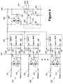
- FIG. 2 a simplified diagram of an exemplary line card 200 including a plurality of subscriber line interface circuits (SLICs) 205. Only the elements of the line card 200 used to support a protective function for SLICs 205 are shown. Exemplary SLIC devices 205 may be model Le79271 devices offered by Zarlink Semiconductor, Inc. of Ontario, Canada. Each SLIC 205 has AD and BD input terminals for the tip and ring lines, respectively, and VBATP and VBATH input terminals for the VBP and VBH reference voltages, respectively. Multiple interface lines 207 are represented in Figure 2 ( i.e ., designated as TIP1- n and RING1- n ).
- Each interface line 207 has protection resistors 210 and a negative overvoltage protector 220 referenced to VBH. Individual negative overvoltage protectors 220 are used for the VBH reference so that the disruption of one interface line 207 does not disrupt the other lines 207, which could potentially cause abnormal noise or loss of service.
- a shared positive overvoltage protector 230 is used for the VBP reference.
- the negative overvoltage protectors 220 operate in a conventional manner, in that when voltages on the tip or ring lines exceed VBH in the negative direction, the associated negative overvoltage protector 220 protects the associated line as described above without affecting the other lines 207.
- the shared positive overvoltage protector 230 performs its protective functions for all of the interface lines 207 in response to one of them having a disruption.
- Gate capacitors 225, 235 are provided at the gate inputs of the protectors 220, 230.
- An isolation diode 240 is provided on the VBATH input terminal of the SLIC 205 to help to trigger the negative overvoltage protector 220 referenced to VBH. Without the diode 240 (i.e ., VBH sinks current for normal operation and cannot source current), the VBH supply can be pulled more and more negative without the negative overvoltage protector 220 being triggered.
- similar diodes are provided for the VBATP input terminals for the SLIC 205, but they are integrated into the SLIC 205.
- Isolation diodes 245 are provided to isolate the tip and ring lines from one another during normal operation.
- An isolation diode 250 works similarly to the isolation diode 240, but the isolation diode 250 helps trigger the shared positive protector 230 in the event of a positive surge. Without the isolation diode 250, the VBP supply may be pushed more and more positive without the shared positive protector 230 being triggered because the VBP supply can source current during normal operation but cannot sink current.
- the shared positive overvoltage protector 230 With the shared positive overvoltage protector 230, the only significant potential for interference between channels is when one channel is hit by a surge while the other channel(s) happened to be in ringing (i.e ., actual power ringing and not the silent period of cadenced ringing). Hence, the ringing waveform of the other channels may be affected, however, the line will still be ringing and will not lose service. Typically, only the sound of the ringing may be affected for a short period of time.
- the shared positive overvoltage protector 230 reduces the cost of the line card 200 and the real estate consumed on the printed circuit board by reducing the number of protectors needed and also the number of gate capacitors 235.
- the potential for disruption of the other lines 207 if they happen to be ringing while there is VPB referenced disruption may be mitigated by providing a power sink 300 in addition to the shared positive overvoltage protector 230.
- the power sink 300 provides a surge current path to ground allowing low current surges, such as low level power cross events, to pass through without triggering the positive overvoltage protector 230.
- the power sink 300 is illustrated as being shared across the multiple interface lines 207, it is contemplated that individual power sinks 300 may be distributed such that each interface line 207 has its own power sink 300.
- the power sink 300 includes a power transistor 310, a power-off loading and operation limiting resistor 320, a bias diode 330, and a bias resistor 340.
- the bias diode 330 and bias resistor 340 bias the power transistor 310 so that the gate of the transistor 310 is referenced to a value of VBP less a diode drop.
- the power transistor 310 conducts current when the voltage on the node 350 exceeds VBP.
- the resistor 320 off loads the power dissipation from the power transistor 310.
- the power transistor 310 saturates when the voltage dropped across the limiting resistor 320 equals VBP less the diode drop of the bias diode 330.
- the current dissipated through the power transistor 310 is limited based on the resistance of the limiting resistor 320. Any remaining current from the disruption causes the voltage at node 350 to increase until it reaches VBP plus a diode drop associated with the positive overvoltage protector 230, thereby turning on the positive overvoltage protector 230 to dissipate the additional current.
- the power sink 300 allows current from low level disruptions to be dissipated without triggering the positive overvoltage protector 230.
- the event is instantaneous.
- the positive overvoltage protector 230 will turn on and take the line 207, along with the positive power supply providing the VBP reference to ground.
- the power supply will go into a self-protection mode. When the surge disappears the power supply will recover from its protected mode and resume normal supply.
- the impact to the VBP supply is limited. Depending on the characteristics of the power supply, the impact may be in the order of 100ms.
- the event can last for an extended time and possibly indefinitely.
- the protection resistors 210 will heat up quickly and transition to a high impedance state.
- the impact to the VBP supply is manageable. For example, it may take 2 seconds for a 50 ohm PTC to become high impedance under a 230 Vrms/300 ohm power cross. In other words, the VBP supply is disrupted and will be at or near 0 V for about 2 seconds.
- the test duration is 15 minutes.
- the protection resistors 210 may take an extended time period to heat up and become high impedance. For example, it may take more than 3 minutes for a 50 ohm PTC to become high impedance under a 100 Vrms / 600 ohm power cross event. It is possible that protection resistors 210 may never become high impedance to release the positive protector and to release the VBP supply.
- the power sink 300 illustrated in Figure 3 helps avoid disrupting the VBP supply for a long time period.
- the power transistor 310 will turn on. If the surge current is less than the capacity of the power sink 300, the positive overvoltage protector 230 will not be triggered, and therefore the surge will not cause disruption to the VBP supply. If the current exceeds the capacity of the power sink 300, the positive overvoltage protector 230 will turn on, taking the VBP supply to ground until the surge event is over, or until the protection resistor 210 become high impedance. As stated above, the surge current exceeding the capacity of the power sink 300 causes the positive overvoltage protector 230 to activate. When the positive overvoltage protector 230 activates, the surge current will jump, resulting in a large current passing through the protection resistor 210, forcing it to become high impedance in a short time.
- the current through the protection resistor 210 at the point at which the positive overvoltage protector 230 turns on is at the maximum capacity of power transistor 310, which is limited by the limiting resistor 320, at the current level about VBP/R 320
- V TIPN VBP (1 + R 210 / R 320 )
- the protection resistor 210 Once the protection resistor 210 is in high impedance, it will release the shared positive overvoltage protector 230 and the VBP supply as well.
- the potential interruption from a low level (i.e ., fault current less than VBP / R 210 + VBP / R 320 ) long lasting fault event is avoided.
- the potential interruption from a high level long lasting fault event is significantly limited only to the very initial portion of the fault event ( i.e ., until the protection resistor 210 is forced into high impedance).
- the power transistor 310 is a relatively large transistor, it can pass through a large current from emitter to collector, I EC , but with typically a low common-emitter current gain, ⁇ .
- the collector current is approximately ⁇ times the base or gate current.
- the gate current may be reduced by providing an enable transistor 360 and its associated resistor 365 in the power sink 300.
- the enable transistor 360 is smaller in size than the power transistor 310 with a higher ⁇ .
- Two bias diodes 330A, 330B are provided to compensate for the transistors 310, 360 with respect to the VBP reference.
- the power transistor 310 When the voltage at the node 350 goes above VBP, the power transistor 310 begins conducting along with the enable transistor 360.
- the enable transistor 360 provides the necessary gate current for the power transistor 310.
- the transistors 310, 365 are off, leaving only the bias circuit including diodes 330A, 330B and the resistor 340 active. Protection diodes 370, 375 are provided to protect the transistors 310, 360 from reverse current flow during a transient.
- the power dissipating capacity of the power sink 300 is limited by the capacity of the power transistor 310.
- the capacity of the power sink 300 may be increased by providing one or more additional power transistors 380 and associated limiting resistors 385 in parallel with the power transistor 310 and its limiting resistor 320.
- An additional protection diode 390 is also provided for the power transistor 380.
- the power transistor 380 is the same size as the power transistor 310, the current carrying capacity of the power sink 300 is effectively doubled, allowing it to handle even higher level transients without activating the positive overvoltage protector 230, and if the surge event does cross the increased current threshold, the current through the protection resistor 210 is further increased, forcing it into high impedance in an even shorter time.
- Sharing protection of the SLICs 205 from positive transients using the shared positive overvoltage protector 230 reduces cost for the line card 200 by reducing the number of protectors 230 and their associated gate capacitors 235. Printed circuit board area savings is also achieved. These advantages may be realized with minimal impact to the overall operation of the line card 200.
- the interference caused by using the shared positive overvoltage protector 230 typically happen only when the disturbed line is in ringing, resulting in a reduction in the AC ringing amplitude. Such disturbances may only happen during a lightning event that occurs during ringing or a high current power cross that initially occurs in the middle of the ringing cycle.
- the affected duration for a lightning strike is only about 100 ms and up to about 2-3 seconds for a power cross fault.
- the affected duration for a power cross fault may be reduced by increasing the sinking current capability of the power sink 300.
- the resulting ringing amplitude reduction may reduce the loudness of the phone in ringing or the ringing amplitude may be too low to ring the phone during the disruption, however, ringing is still going on and there will be no service drop.
- the distortions to the ringing typically affect only one ringing cadence cycle.
Description
- The disclosed subject matter relates generally to telecommunications and, more particularly, to a method and apparatus for shared positive protection.
- In communications systems, particularly telephony, it is common practice to transmit signals between a subscriber station and a central switching office via a two-wire bi-directional communication channel. A line card generally connects the subscriber station to the central switching office. A line card typically includes at least one subscriber line interface circuit (SLIC) as well as a subscriber line audio-processing circuit (SLAC). The functions of the line card include range from supplying talk battery to performing wake-up sequences of circuits to allow communications to take place.
- Subscriber line interface circuits (SLICs) have been developed to provide an interface between a low voltage signal path in a telephone central office and a high-voltage telephone subscriber line. The SLIC provides functions such as off hook detection, ringing signal generation, and battery feed to the subscriber line. The subscriber line consists of a telephone transmission line, including two conductors referred to as A and B or tip and ring, and the subscriber telephone equipment coupled across the tip and ring conductors (i.e., the load). The subscriber line and the subscriber telephone equipment are also referred to as a subscriber loop.
- The SLIC provides power from the telephone central office to the subscriber line in response to a received battery voltage. The battery voltage is a DC voltage supplied to the SLIC to power the SLIC and the subscriber line. The SLIC supplies a DC current at the battery voltage to the subscriber line. Superimposed on the DC current are AC signals of audio frequency by which information is conveyed between the subscriber and the central office. The battery voltage is generated at the central office, either by a depletable energy storage device such as a battery or by a DC generator, for supply to the SLIC. In a central office, one battery or DC generator supplies the battery voltage to many SLICs and their associated subscriber loops.
- To meet safety requirements it is common to use a positive battery, VBP, along with a negative battery, VBH, to generate sufficient voltage for ringing generation. To save power and reduce power dissipation on the SLIC for short loop applications, a third supply is often used for DC feed along with VBH. The third supply is typically lower in amplitude than VBH, and is often referred to as VBL.
- To protect the SLIC from voltage excursions, such as lightning surges or power cross events, a protection scheme is employed to connect the tip or ring line experiencing the event to ground. Typically one protector is employed to track the VBP supply and another protector that tracks the VBH supply.
-
Figure 1 is a circuit diagram illustrating aconventional protection circuit 100. InFigure 1 , multiple interface-lines 105 for interfacing with external subscriber lines are shown (i.e., designated as TIP1-n and RING1-n). Eachinterface line 105 hasprotection resistors 110, anegative overvoltage protector 120 referenced to VBH, and apositive overvoltage protector 130 referenced to VBP. Exemplary overvoltage protectors are available commercially, such as a TISP8200M device for thenegative overvoltage protector 120 and a TISP8201 M for thepositive overvoltage protector 130, both offered by Bourns, Inc. of Riverside, CA.Gate capacitors protectors protectors - The
negative overvoltage protector 120 initially clips overvoltages close to the VBH value. If sufficient current is available from the overvoltage, then thenegative overvoltage protector 120 will crowbar into a low voltage ground referenced on-state condition. As the overvoltage subsides, the high holding current of thenegative overvoltage protector 120 prevents DC latchup with the SLIC output current. Similarly, thepositive overvoltage protector 130 initially clips positive overvoltages close to the VBP value. If sufficient current is available from the overvoltage, then thepositive overvoltage protector 130 will crowbar into a low voltage ground referenced on-state condition. As the overvoltage subsides the SLIC pulls the conductor voltage down to its normal negative value and this commutates thepositive overvoltage protector 130 into a reverse biased condition. During an overvoltage transient, increased current may pass through theprotection resistors 110, which are positive coefficient devices, causing them to tri-state and thereby isolate the associatedinterface line 105. - The dual protector protection scheme of
Figure 1 is costly, since each interface line supported by a line card requires twoprotectors expensive gate capacitors -
US 2009/0092243 describes a line card with a plurality of subscriber line interface circuits. -
WO 03/026093 - This section of this document is intended to introduce various aspects of art that may be related to various aspects of the disclosed subject matter described and/or claimed below. This section provides background information to facilitate a better understanding of the various aspects of the disclosed subject matter. It should be understood that the statements in this section of this document are to be read in this light, and not as admissions of prior art. The disclosed subject matter is directed to overcoming, or at least reducing the effects of, one or more of the problems set forth above.
- The following presents a simplified summary of the disclosed subject matter in order to provide a basic understanding of some aspects of the disclosed subject matter. This summary is not an exhaustive overview of the disclosed subject matter. It is not intended to identify key or critical elements of the disclosed subject matter or to delineate the scope of the disclosed subject matter. Its sole purpose is to present some concepts in a simplified form as a prelude to the more detailed description that is discussed later.
- One aspect of the disclosed subject matter is seen in a line card including a plurality of subscriber line interface circuits, a plurality of interface lines, and a first positive overvoltage protector. The subscriber line interface circuits each have a first input terminal operable to receive power at a first positive reference voltage for generating a ringing signal. The interface lines are each coupled to one of the subscriber line interface circuits for interfacing with subscriber lines external to the line card. The first positive overvoltage protector is coupled to the interface lines, shared across the subscriber line interface circuits and referenced to the first positive reference voltage to provide overvoltage protection responsive to a voltage on at least one of the interface lines exceeding the first positive reference voltage.
- The first overvoltage protector may include a first gate input terminal coupled to receive the first reference voltage, the line card further comprising a first gate capacitor coupled to the first gate input terminal.
- The first overvoltage protector may be operable to provide overvoltage protection by grounding the interface lines responsive to a voltage on at least one of the interface lines exceeding the first positive reference voltage.
- The line card may further comprise an isolation diode coupled between each of the interface lines and the first overvoltage protector.
- The subscriber line interface circuits each have a second input terminal operable to receive power at a second negative reference voltage, and the line card further comprises: a plurality of second overvoltage protectors referenced to the second negative reference voltage, wherein each of the second overvoltage protectors is coupled to an associated one of the interface lines and is operable to provide overvoltage protection responsive to a voltage on the associated interface line exceeding the second negative reference voltage.
- The first overvoltage protector may include a first gate input terminal coupled to receive the first positive reference voltage and the second overvoltage protectors each may include a second gate input terminal coupled to receive the second negative reference voltage, the line card preferably further comprising: a first gate capacitor coupled to the first gate input terminal; and a plurality of second gate capacitors, each coupled to one of the second gate input terminals.
- The first overvoltage protector may be operable to provide overvoltage protection by grounding the interface lines responsive to a voltage on at least one of the interface lines exceeding the first positive reference voltage, and the second overvoltage protectors may each be operable to provide overvoltage protection by grounding its associated interface line responsive to a voltage on the associated interface lines exceeding the second negative reference voltage.
- The line card preferably further comprises at least one protection resistor coupled to each of the interface lines.
- Another aspect of the disclosed subject matter is seen in a method for protecting a line card including a plurality of interface lines and a plurality of subscriber line interface circuits operable to receive power at a first positive reference voltage for generating a ringing signal and each coupled to one pair of the interface lines for interfacing with external subscriber lines. The method includes monitoring a voltage on the interface lines, and employing a first positive overvoltage protector coupled to the interface lines, shared across the subscriber line interface circuits, and being operable to couple the interface lines to ground responsive to determining that the voltage on any one of the interface lines exceeds a first positive reference voltage; and employing a plurality of second negative overvoltage protectors, each coupled to one of the interface lines and being operable to couple a selected interface line to ground using the negative overvoltage protector coupled to the selected interface line responsive to determining that the voltage on the selected interface line exceeds a second negative reference voltage.
- The method may further comprise coupling a selected interface line subscriber to ground responsive to determining that the voltage on the selected interface line exceeds a second positive reference voltage.
- The disclosed subject matter will hereafter be described with reference to the accompanying drawings, wherein like reference numerals denote like elements, and:
-
Figure 1 is a diagram of a conventional protection circuit for a line card; -
Figure 2 is a diagram of a protection circuit for a line card employing shared positive protection in accordance with one illustrative embodiment of the present subject matter; -
Figure 3 is a diagram of an embodiment of the protection circuit ofFigure 2 including an additional power sink; -
Figure 4 is a diagram of an embodiment of the protection circuit ofFigure 3 including an additional transistor in the sink circuit for reducing the constant gate current requirements; and -
Figure 5 is a diagram of an embodiment of the protection circuit ofFigure 4 including an additional power transistor in the sink circuit for increasing the current shunting capacity. - While the disclosed subject matter is susceptible to various modifications and alternative forms, specific embodiments thereof have been shown by way of example in the drawings and are herein described in detail. It should be understood, however, that the description herein of specific embodiments is not intended to limit the disclosed subject matter to the particular forms disclosed, but on the contrary, the intention is to cover all modifications, equivalents, and alternatives falling within the spirit and scope of the disclosed subject matter as defined by the appended claims.
- One or more specific embodiments of the disclosed subject matter will be described below. It is specifically intended that the disclosed subject matter not be limited to the embodiments and illustrations contained herein, but include modified forms of those embodiments including portions of the embodiments and combinations of elements of different embodiments as come within the scope of the following claims. It should be appreciated that in the development of any such actual implementation, as in any engineering or design project, numerous implementation-specific decisions must be made to achieve the developers' specific goals, such as compliance with system-related and business related constraints, which may vary from one implementation to another. Moreover, it should be appreciated that such a development effort might be complex and time consuming, but would nevertheless be a routine undertaking of design, fabrication, and manufacture for those of ordinary skill having the benefit of this disclosure. Nothing in this application is considered critical or essential to the disclosed subject matter unless explicitly indicated as being "critical" or "essential"
- The disclosed subject matter will now be described with reference to the attached figures. Various structures, systems and devices are schematically depicted in the drawings for purposes of explanation only and so as to not obscure the disclosed subject matter with details that are well known to those skilled in the art. Nevertheless, the attached drawings are included to describe and explain illustrative examples of the disclosed subject matter. The words and phrases used herein should be understood and interpreted to have a meaning consistent with the understanding of those words and phrases by those skilled in the relevant art. No special definition of a term or phrase, i.e., a definition that is different from the ordinary and customary meaning as understood by those skilled in the art, is intended to be implied by consistent usage of the term or phrase herein. To the extent that a term or phrase is intended to have a special meaning, i.e., a meaning other than that understood by skilled artisans, such a special definition will be expressly set forth in the specification in a definitional manner that directly and unequivocally provides the special definition for the term or phrase.
- Referring now to the drawings wherein like reference numbers correspond to similar components throughout the several views and, specifically, referring to
Figure 2 , the disclosed subject matter shall be described in the context of a simplified diagram of anexemplary line card 200 including a plurality of subscriber line interface circuits (SLICs) 205. Only the elements of theline card 200 used to support a protective function forSLICs 205 are shown.Exemplary SLIC devices 205 may be model Le79271 devices offered by Zarlink Semiconductor, Inc. of Ontario, Canada. EachSLIC 205 has AD and BD input terminals for the tip and ring lines, respectively, and VBATP and VBATH input terminals for the VBP and VBH reference voltages, respectively.Multiple interface lines 207 are represented inFigure 2 (i.e., designated as TIP1-n and RING1-n). - Each
interface line 207 hasprotection resistors 210 and anegative overvoltage protector 220 referenced to VBH. Individual negativeovervoltage protectors 220 are used for the VBH reference so that the disruption of oneinterface line 207 does not disrupt theother lines 207, which could potentially cause abnormal noise or loss of service. - Because the VBP source is typically used only for ringing, disruptions on one external subscriber line are unlikely to cause significant effects on the other subscriber lines. Hence, a shared
positive overvoltage protector 230 is used for the VBP reference. Thenegative overvoltage protectors 220 operate in a conventional manner, in that when voltages on the tip or ring lines exceed VBH in the negative direction, the associatednegative overvoltage protector 220 protects the associated line as described above without affecting theother lines 207. The sharedpositive overvoltage protector 230 performs its protective functions for all of theinterface lines 207 in response to one of them having a disruption.Gate capacitors protectors - An
isolation diode 240 is provided on the VBATH input terminal of theSLIC 205 to help to trigger thenegative overvoltage protector 220 referenced to VBH. Without the diode 240 (i.e., VBH sinks current for normal operation and cannot source current), the VBH supply can be pulled more and more negative without thenegative overvoltage protector 220 being triggered. In the illustrated embodiment, similar diodes are provided for the VBATP input terminals for theSLIC 205, but they are integrated into theSLIC 205.Isolation diodes 245 are provided to isolate the tip and ring lines from one another during normal operation. Anisolation diode 250 works similarly to theisolation diode 240, but theisolation diode 250 helps trigger the sharedpositive protector 230 in the event of a positive surge. Without theisolation diode 250, the VBP supply may be pushed more and more positive without the sharedpositive protector 230 being triggered because the VBP supply can source current during normal operation but cannot sink current. - With the shared
positive overvoltage protector 230, the only significant potential for interference between channels is when one channel is hit by a surge while the other channel(s) happened to be in ringing (i.e., actual power ringing and not the silent period of cadenced ringing). Hence, the ringing waveform of the other channels may be affected, however, the line will still be ringing and will not lose service. Typically, only the sound of the ringing may be affected for a short period of time. The sharedpositive overvoltage protector 230 reduces the cost of theline card 200 and the real estate consumed on the printed circuit board by reducing the number of protectors needed and also the number ofgate capacitors 235. - As shown in the embodiment of
Figure 3 , the potential for disruption of theother lines 207 if they happen to be ringing while there is VPB referenced disruption may be mitigated by providing apower sink 300 in addition to the sharedpositive overvoltage protector 230. Thepower sink 300 provides a surge current path to ground allowing low current surges, such as low level power cross events, to pass through without triggering thepositive overvoltage protector 230. Although thepower sink 300 is illustrated as being shared across themultiple interface lines 207, it is contemplated that individual power sinks 300 may be distributed such that eachinterface line 207 has itsown power sink 300. - The
power sink 300 includes apower transistor 310, a power-off loading andoperation limiting resistor 320, abias diode 330, and abias resistor 340. Thebias diode 330 andbias resistor 340 bias thepower transistor 310 so that the gate of thetransistor 310 is referenced to a value of VBP less a diode drop. Hence, thepower transistor 310 conducts current when the voltage on thenode 350 exceeds VBP. As the voltage atnode 350 continues to attempt to rise due to a positive disruption, the current conducted by thepower transistor 310 increases. The power dissipated in theresistor 320 also increases as P320 = R320 * I2. The power dissipation in thetransistor 310 is reduced from P310 = VBP * I without theresistor 320 to P310 = (VBP - R320 * I) * I = VBP * I - R320 * I2 = VBP * I - P320 with theresistor 320. Thus theresistor 320 off loads the power dissipation from thepower transistor 310. Thepower transistor 310 saturates when the voltage dropped across the limitingresistor 320 equals VBP less the diode drop of thebias diode 330. Hence, the current dissipated through thepower transistor 310 is limited based on the resistance of the limitingresistor 320. Any remaining current from the disruption causes the voltage atnode 350 to increase until it reaches VBP plus a diode drop associated with thepositive overvoltage protector 230, thereby turning on thepositive overvoltage protector 230 to dissipate the additional current. - Hence, the
power sink 300 allows current from low level disruptions to be dissipated without triggering thepositive overvoltage protector 230. For a lightning surge, the event is instantaneous. For such a positive surge with large current but short duration, thepositive overvoltage protector 230 will turn on and take theline 207, along with the positive power supply providing the VBP reference to ground. The power supply will go into a self-protection mode. When the surge disappears the power supply will recover from its protected mode and resume normal supply. The impact to the VBP supply is limited. Depending on the characteristics of the power supply, the impact may be in the order of 100ms. - For power cross, however, the event can last for an extended time and possibly indefinitely. In the K.20/K.44 and GR1089 standards there are many tests that last 15 minutes, however, in the real world a power cross event could last much longer. For those cases where the power cross levels are high and the source impedances are low, the
protection resistors 210 will heat up quickly and transition to a high impedance state. The impact to the VBP supply is manageable. For example, it may take 2 seconds for a 50 ohm PTC to become high impedance under a 230 Vrms/300 ohm power cross. In other words, the VBP supply is disrupted and will be at or near 0 V for about 2 seconds. - For those cases where the power cross level is low and/or the source impedance is high, such as a 230 Vrms / 1000 ohm event or a 100 Vrms / 600 ohm event, the test duration is 15 minutes. Because of the low current the
protection resistors 210 may take an extended time period to heat up and become high impedance. For example, it may take more than 3 minutes for a 50 ohm PTC to become high impedance under a 100 Vrms / 600 ohm power cross event. It is possible thatprotection resistors 210 may never become high impedance to release the positive protector and to release the VBP supply. Thepower sink 300 illustrated inFigure 3 helps avoid disrupting the VBP supply for a long time period. - In the event of a positive surge, the
power transistor 310 will turn on. If the surge current is less than the capacity of thepower sink 300, thepositive overvoltage protector 230 will not be triggered, and therefore the surge will not cause disruption to the VBP supply. If the current exceeds the capacity of thepower sink 300, thepositive overvoltage protector 230 will turn on, taking the VBP supply to ground until the surge event is over, or until theprotection resistor 210 become high impedance. As stated above, the surge current exceeding the capacity of thepower sink 300 causes thepositive overvoltage protector 230 to activate. When thepositive overvoltage protector 230 activates, the surge current will jump, resulting in a large current passing through theprotection resistor 210, forcing it to become high impedance in a short time. The current through theprotection resistor 210 at the point at which thepositive overvoltage protector 230 turns on is at the maximum capacity ofpower transistor 310, which is limited by the limitingresistor 320, at the current level about VBP/R320 This same current is going through theprotection resistor 210 as (VTIPN - V350) / R210 or about (VTIPN - VBP) / R210. Therefore VBP / R320 = (VTIPN - VBP) / R210. VTIPN can be determined by VTIPN = VBP (1 + R210 / R320). When thepositive overvoltage protector 230 turns on, thenode 350 is taken to ground. The current through theprotection resistor 210 will be (VTIPN - 0) / R210 = VTIPN / R210. With the known VTIPN the current can be determined as VTIPN / R210 = VBP (1 + R210 / R320) / R210 = VBP / R210 + VBP / R320. Therefore, the current jumps from VBP / R320 to (VBP / R210 + VBP / R320). If VBP = 100V, R210 = 50 ohms, and R320 = 100 ohms, the current will jump from 1 ampere to 3 amperes. - The above analysis implies that the
power sink 300 with its current capacity of VBP / R320 is blocking otherwise surge current of (VBP / R210 + VBP / R320) from triggering the positive protector. Since values of R210 = 50 ohms and R320 = 100 ohms are typical,power sink 300 is blocking a surge current 3 times its current capability from triggering thepositive overvoltage protector 230. In another words,power sink 300 effectively creates a high threshold. Below the threshold, thepositive overvoltage protector 230 will not be triggered. If a long-lasting event that does cross the threshold occurs, the large current will quickly force theprotection resistor 210 into high impedance. Once theprotection resistor 210 is in high impedance, it will release the sharedpositive overvoltage protector 230 and the VBP supply as well. The potential interruption from a low level (i.e., fault current less than VBP / R210 + VBP / R320) long lasting fault event is avoided. The potential interruption from a high level long lasting fault event is significantly limited only to the very initial portion of the fault event (i.e., until theprotection resistor 210 is forced into high impedance). - Because the
power transistor 310 is a relatively large transistor, it can pass through a large current from emitter to collector, IEC, but with typically a low common-emitter current gain, β. The collector current is approximately β times the base or gate current. The gate current can be significant as IG = IEC / β. The bias circuit including thediode 330 and thebias resistor 340 will have to constantly provide no less than the peak gate current. This situation may consume a significant levels of power, as most of time, there is no surge fault. If VBP = 100 V and R320 = 100 ohms, the peak IEC = 1 A. If β = 10, then the gate current IG = 100mA. The power dissipate in theresistor 340 would have to be at least IG* VBP or 100mA * 100V = 10 watts. - As shown in another embodiment illustrated in
Figure 4 , the gate current may be reduced by providing an enabletransistor 360 and its associatedresistor 365 in thepower sink 300. The enabletransistor 360 is smaller in size than thepower transistor 310 with a higher β. The bias current is now greatly reduced from IG310 to IG310 / β365. Assuming β365 is 50, the bias current will be I310 / β365 = 100 mA / 50 = 2 mA. The bias power on thebias resistor 340 is reduced from 10 watts to 2 mA * 100 V = 0.2 watts. Twobias diodes transistors node 350 goes above VBP, thepower transistor 310 begins conducting along with the enabletransistor 360. The enabletransistor 360 provides the necessary gate current for thepower transistor 310. However, during normal operation with no surge transients thetransistors circuit including diodes resistor 340 active.Protection diodes transistors - The power dissipating capacity of the
power sink 300 is limited by the capacity of thepower transistor 310. In yet another embodiment illustrated inFigure 5 , the capacity of thepower sink 300 may be increased by providing one or moreadditional power transistors 380 and associated limitingresistors 385 in parallel with thepower transistor 310 and its limitingresistor 320. Anadditional protection diode 390 is also provided for thepower transistor 380. If thepower transistor 380 is the same size as thepower transistor 310, the current carrying capacity of thepower sink 300 is effectively doubled, allowing it to handle even higher level transients without activating thepositive overvoltage protector 230, and if the surge event does cross the increased current threshold, the current through theprotection resistor 210 is further increased, forcing it into high impedance in an even shorter time. - Sharing protection of the
SLICs 205 from positive transients using the sharedpositive overvoltage protector 230 reduces cost for theline card 200 by reducing the number ofprotectors 230 and their associatedgate capacitors 235. Printed circuit board area savings is also achieved. These advantages may be realized with minimal impact to the overall operation of theline card 200. The interference caused by using the sharedpositive overvoltage protector 230 typically happen only when the disturbed line is in ringing, resulting in a reduction in the AC ringing amplitude. Such disturbances may only happen during a lightning event that occurs during ringing or a high current power cross that initially occurs in the middle of the ringing cycle. The affected duration for a lightning strike is only about 100 ms and up to about 2-3 seconds for a power cross fault. The affected duration for a power cross fault may be reduced by increasing the sinking current capability of thepower sink 300. In case of an interruption to the VBP power supply while adifferent interface line 207 happens to be in ringing, the resulting ringing amplitude reduction may reduce the loudness of the phone in ringing or the ringing amplitude may be too low to ring the phone during the disruption, however, ringing is still going on and there will be no service drop. In other words, the distortions to the ringing typically affect only one ringing cadence cycle. - The particular embodiments disclosed above are illustrative only, as the disclosed subject matter may be modified and practiced in different but equivalent manners apparent to those skilled in the art having the benefit of the teachings herein. Furthermore, no limitations are intended to the details of construction or design herein shown, other than as described in the claims below. It is therefore evident that the particular embodiments disclosed above may be altered or modified and all such variations are considered within the scope of the disclosed subject matter. Accordingly, the protection sought herein is as set forth in the claims below.
Claims (8)
- A line card (200), comprising:a plurality of subscriber line interface circuits (205) each having a first input terminal operable to receive power at a first positive reference voltage for generating a ringing signal and a second input terminal operable to receive power at a second negative reference voltage;a plurality of interface lines (207) each coupled to one of the subscriber line interface circuits (205) for interfacing with subscriber lines external to the line card (200); and characterized bya first positive overvoltage protector (230) coupled to the interface lines (207), shared across the subscriber line interface circuits (205) and referenced to the first positive reference voltage to provide positive overvoltage protection responsive to a voltage on at least one of the interface lines (207) exceeding the first positive reference voltage; anda plurality of second negative overvoltage protectors (220) referenced to the second negative reference voltage, wherein each of the second negative overvoltage protectors (220) is coupled to an associated one of the interface lines (207) and is operable to provide negative overvoltage protection responsive to a voltage on the associated interface line (207) exceeding the second negative reference voltage.
- The line card (200) of claim 1, wherein the first positive overvoltage protector (230) includes a first gate input terminal coupled to receive the first reference voltage, further comprising a first gate capacitor (235) coupled to the first gate input terminal.
- The line card (200) of claim 1 or 2, wherein the first positive overvoltage protector (230) is operable to provide overvoltage protection by grounding the interface lines (207) responsive to a voltage on at least one of the interface lines (207) exceeding the first positive reference voltage.
- The line card (200) of claim 1, 2 or 3, further comprising an isolation diode (245) coupled between each of the interface lines (207) and the first positive overvoltage protector (230).
- The line card (200) of any preceding claim, wherein the first positive overvoltage protector (230) includes a first gate input terminal coupled to receive the first positive reference voltage and the second overvoltage protectors (220) each include a second gate input terminal coupled to receive the second negative reference voltage, further comprising:a first gate capacitor (235) coupled to the first gate input terminal; anda plurality of second gate capacitors (225), each coupled to one of the second gate input terminals.
- The line card (200) of any preceding claim, wherein the first positive overvoltage protector (230) is operable to provide overvoltage protection by grounding the interface lines (207) responsive to a voltage on at least one of the interface lines (207) exceeding the first positive reference voltage, and the second negative overvoltage protectors (220) are each operable to provide overvoltage protection by grounding its associated interface line (207) responsive to a voltage on the associated interface lines (207) exceeding the second negative reference voltage.
- The line card (200) of any preceding claim, further comprising at least one protection resistor (210) coupled to each of the interface lines (207).
- A method for protecting a line card (200) including a plurality of interface lines (207) for interfacing with external subscriber lines and a plurality of subscriber line interface circuits (205) operable to receive power at a first positive reference voltage for generating a ringing signal and to receive power at a second negative reference voltage, each being coupled to one pair of the interface lines (207), the method comprising:monitoring a voltage on the interface lines (207); and characterized byemploying a first positive overvoltage protector (230) coupled to the interface lines (207), shared across the subscriber line interface circuits (205), and being operable to couple the interface lines (207) to ground responsive to determining that the voltage on any one of the interface lines (207) exceeds a first positive reference voltage; andemploying a plurality of second negative overvoltage protectors (220), each coupled to one of the interface lines (207) and being operable to couple a selected interface line (207) to ground using the negative overvoltage protector (220) coupled to the selected interface line (207) responsive to determining that the voltage on the selected interface line (207) exceeds a second negative reference voltage.
Applications Claiming Priority (1)
| Application Number | Priority Date | Filing Date | Title |
|---|---|---|---|
| US12/550,782 US8442213B2 (en) | 2009-08-31 | 2009-08-31 | Method and apparatus for shared positive protection |
Publications (3)
| Publication Number | Publication Date |
|---|---|
| EP2290937A2 EP2290937A2 (en) | 2011-03-02 |
| EP2290937A3 EP2290937A3 (en) | 2011-04-13 |
| EP2290937B1 true EP2290937B1 (en) | 2016-01-27 |
Family
ID=43384685
Family Applications (1)
| Application Number | Title | Priority Date | Filing Date |
|---|---|---|---|
| EP10251469.2A Active EP2290937B1 (en) | 2009-08-31 | 2010-08-19 | Method and apparatus for controlling shared positive protection |
Country Status (4)
| Country | Link |
|---|---|
| US (1) | US8442213B2 (en) |
| EP (1) | EP2290937B1 (en) |
| JP (1) | JP5220819B2 (en) |
| KR (1) | KR20110023828A (en) |
Families Citing this family (1)
| Publication number | Priority date | Publication date | Assignee | Title |
|---|---|---|---|---|
| CN102956426A (en) * | 2011-08-22 | 2013-03-06 | 北京中科信电子装备有限公司 | Extraction inhibiting surge protector |
Family Cites Families (5)
| Publication number | Priority date | Publication date | Assignee | Title |
|---|---|---|---|---|
| DE3215551A1 (en) * | 1982-04-26 | 1983-10-27 | Siemens AG, 1000 Berlin und 8000 München | CIRCUIT ARRANGEMENT FOR OVERVOLTAGE PROTECTION OF INTERFACE CIRCUITS |
| JPH0662445A (en) * | 1991-05-13 | 1994-03-04 | Fujitsu Ltd | Overvoltage protecting circuit |
| JPH06178339A (en) * | 1992-12-07 | 1994-06-24 | Toshiba Corp | Line interface protection circuit |
| US6882514B2 (en) * | 2001-09-14 | 2005-04-19 | Arris International, Inc. | Overcurrent and overvoltage protection method and architecture for a tip and ring subscriber line interface circuit |
| US20090092243A1 (en) * | 2007-10-09 | 2009-04-09 | Infineon Technologies Ag | Protection Circuit and Method |
-
2009
- 2009-08-31 US US12/550,782 patent/US8442213B2/en active Active
-
2010
- 2010-08-19 EP EP10251469.2A patent/EP2290937B1/en active Active
- 2010-08-30 KR KR1020100084079A patent/KR20110023828A/en not_active Application Discontinuation
- 2010-08-30 JP JP2010191826A patent/JP5220819B2/en active Active
Also Published As
| Publication number | Publication date |
|---|---|
| JP2011055492A (en) | 2011-03-17 |
| JP5220819B2 (en) | 2013-06-26 |
| US8442213B2 (en) | 2013-05-14 |
| EP2290937A2 (en) | 2011-03-02 |
| KR20110023828A (en) | 2011-03-08 |
| US20110051925A1 (en) | 2011-03-03 |
| EP2290937A3 (en) | 2011-04-13 |
Similar Documents
| Publication | Publication Date | Title |
|---|---|---|
| US7433165B2 (en) | Auto-resetting span-power protection | |
| US7859814B2 (en) | Linear low capacitance overvoltage protection circuit using a blocking diode | |
| EP2672656B1 (en) | Power over ethernet port protection circuit and ethernet power supply equipment | |
| US6882514B2 (en) | Overcurrent and overvoltage protection method and architecture for a tip and ring subscriber line interface circuit | |
| WO2015096398A1 (en) | Poe power supply protection system and method | |
| JPH10507059A (en) | Protection of active telephone line interface circuits | |
| US7706526B2 (en) | Method and apparatus for powering electronics associated with a telephone line twisted pair | |
| US7715165B2 (en) | System and method of surge protection in a powered device | |
| US7375942B1 (en) | Flexible secondary overcurrent protection | |
| US8406417B2 (en) | Overvoltage protection with power sink | |
| US20010001619A1 (en) | High current protection circuit for telephone interface | |
| US20050220021A1 (en) | Methods and arrangement for power transmission over telephone lines | |
| EP2290937B1 (en) | Method and apparatus for controlling shared positive protection | |
| US6606231B2 (en) | Integrated telephony subscriber line protection and filter device | |
| US6922323B1 (en) | Protection circuitry for a subscriber line interface circuit (SLIC) arrangement | |
| US20110033039A1 (en) | Method and apparatus for controlling ringing voltage | |
| US20020101980A1 (en) | Protection of subscriber line interface circuits (SLICS) without degradation in longitudinal balance | |
| US6628497B1 (en) | Overvoltage protector bridge circuit | |
| US8194853B2 (en) | Surge immunity circuit for telecom DDA | |
| US7907381B2 (en) | Protection circuit for a subscriber line interface circuit | |
| US8705728B2 (en) | Shared protection scheme for multiple variable batteries | |
| US8437111B1 (en) | Systems and methods for current limiting with overload protection | |
| US10027111B1 (en) | Auxiliary circuit for overvoltage protection | |
| CN111525499A (en) | Electronic device | |
| WO2002021658A1 (en) | Method and apparatus for protecting multiple telephone lines |
Legal Events
| Date | Code | Title | Description |
|---|---|---|---|
| PUAI | Public reference made under article 153(3) epc to a published international application that has entered the european phase |
Free format text: ORIGINAL CODE: 0009012 |
|
| AK | Designated contracting states |
Kind code of ref document: A2 Designated state(s): AL AT BE BG CH CY CZ DE DK EE ES FI FR GB GR HR HU IE IS IT LI LT LU LV MC MK MT NL NO PL PT RO SE SI SK SM TR |
|
| AX | Request for extension of the european patent |
Extension state: BA ME RS |
|
| REG | Reference to a national code |
Ref country code: DE Ref legal event code: R079 Ref document number: 602010030323 Country of ref document: DE Free format text: PREVIOUS MAIN CLASS: H04M0003180000 Ipc: H04M0003000000 |
|
| PUAL | Search report despatched |
Free format text: ORIGINAL CODE: 0009013 |
|
| AK | Designated contracting states |
Kind code of ref document: A3 Designated state(s): AL AT BE BG CH CY CZ DE DK EE ES FI FR GB GR HR HU IE IS IT LI LT LU LV MC MK MT NL NO PL PT RO SE SI SK SM TR |
|
| AX | Request for extension of the european patent |
Extension state: BA ME RS |
|
| RIC1 | Information provided on ipc code assigned before grant |
Ipc: H04M 3/18 20060101ALI20110309BHEP Ipc: H04M 3/00 20060101AFI20110309BHEP |
|
| 17P | Request for examination filed |
Effective date: 20111013 |
|
| 17Q | First examination report despatched |
Effective date: 20140707 |
|
| RAP1 | Party data changed (applicant data changed or rights of an application transferred) |
Owner name: MICROSEMI SEMICONDUCTOR (U.S.) INC. |
|
| GRAP | Despatch of communication of intention to grant a patent |
Free format text: ORIGINAL CODE: EPIDOSNIGR1 |
|
| INTG | Intention to grant announced |
Effective date: 20150713 |
|
| GRAP | Despatch of communication of intention to grant a patent |
Free format text: ORIGINAL CODE: EPIDOSNIGR1 |
|
| INTG | Intention to grant announced |
Effective date: 20150903 |
|
| GRAS | Grant fee paid |
Free format text: ORIGINAL CODE: EPIDOSNIGR3 |
|
| GRAA | (expected) grant |
Free format text: ORIGINAL CODE: 0009210 |
|
| AK | Designated contracting states |
Kind code of ref document: B1 Designated state(s): AL AT BE BG CH CY CZ DE DK EE ES FI FR GB GR HR HU IE IS IT LI LT LU LV MC MK MT NL NO PL PT RO SE SI SK SM TR |
|
| REG | Reference to a national code |
Ref country code: GB Ref legal event code: FG4D |
|
| REG | Reference to a national code |
Ref country code: CH Ref legal event code: EP |
|
| REG | Reference to a national code |
Ref country code: AT Ref legal event code: REF Ref document number: 773162 Country of ref document: AT Kind code of ref document: T Effective date: 20160215 |
|
| REG | Reference to a national code |
Ref country code: IE Ref legal event code: FG4D |
|
| REG | Reference to a national code |
Ref country code: DE Ref legal event code: R096 Ref document number: 602010030323 Country of ref document: DE |
|
| REG | Reference to a national code |
Ref country code: LT Ref legal event code: MG4D |
|
| REG | Reference to a national code |
Ref country code: NL Ref legal event code: MP Effective date: 20160127 |
|
| REG | Reference to a national code |
Ref country code: AT Ref legal event code: MK05 Ref document number: 773162 Country of ref document: AT Kind code of ref document: T Effective date: 20160127 |
|
| PG25 | Lapsed in a contracting state [announced via postgrant information from national office to epo] |
Ref country code: NL Free format text: LAPSE BECAUSE OF FAILURE TO SUBMIT A TRANSLATION OF THE DESCRIPTION OR TO PAY THE FEE WITHIN THE PRESCRIBED TIME-LIMIT Effective date: 20160127 |
|
| REG | Reference to a national code |
Ref country code: FR Ref legal event code: PLFP Year of fee payment: 7 |
|
| PG25 | Lapsed in a contracting state [announced via postgrant information from national office to epo] |
Ref country code: FI Free format text: LAPSE BECAUSE OF FAILURE TO SUBMIT A TRANSLATION OF THE DESCRIPTION OR TO PAY THE FEE WITHIN THE PRESCRIBED TIME-LIMIT Effective date: 20160127 Ref country code: HR Free format text: LAPSE BECAUSE OF FAILURE TO SUBMIT A TRANSLATION OF THE DESCRIPTION OR TO PAY THE FEE WITHIN THE PRESCRIBED TIME-LIMIT Effective date: 20160127 Ref country code: ES Free format text: LAPSE BECAUSE OF FAILURE TO SUBMIT A TRANSLATION OF THE DESCRIPTION OR TO PAY THE FEE WITHIN THE PRESCRIBED TIME-LIMIT Effective date: 20160127 Ref country code: GR Free format text: LAPSE BECAUSE OF FAILURE TO SUBMIT A TRANSLATION OF THE DESCRIPTION OR TO PAY THE FEE WITHIN THE PRESCRIBED TIME-LIMIT Effective date: 20160428 Ref country code: NO Free format text: LAPSE BECAUSE OF FAILURE TO SUBMIT A TRANSLATION OF THE DESCRIPTION OR TO PAY THE FEE WITHIN THE PRESCRIBED TIME-LIMIT Effective date: 20160427 Ref country code: IT Free format text: LAPSE BECAUSE OF FAILURE TO SUBMIT A TRANSLATION OF THE DESCRIPTION OR TO PAY THE FEE WITHIN THE PRESCRIBED TIME-LIMIT Effective date: 20160127 |
|
| PG25 | Lapsed in a contracting state [announced via postgrant information from national office to epo] |
Ref country code: SE Free format text: LAPSE BECAUSE OF FAILURE TO SUBMIT A TRANSLATION OF THE DESCRIPTION OR TO PAY THE FEE WITHIN THE PRESCRIBED TIME-LIMIT Effective date: 20160127 Ref country code: PT Free format text: LAPSE BECAUSE OF FAILURE TO SUBMIT A TRANSLATION OF THE DESCRIPTION OR TO PAY THE FEE WITHIN THE PRESCRIBED TIME-LIMIT Effective date: 20160527 Ref country code: LT Free format text: LAPSE BECAUSE OF FAILURE TO SUBMIT A TRANSLATION OF THE DESCRIPTION OR TO PAY THE FEE WITHIN THE PRESCRIBED TIME-LIMIT Effective date: 20160127 Ref country code: PL Free format text: LAPSE BECAUSE OF FAILURE TO SUBMIT A TRANSLATION OF THE DESCRIPTION OR TO PAY THE FEE WITHIN THE PRESCRIBED TIME-LIMIT Effective date: 20160127 Ref country code: LV Free format text: LAPSE BECAUSE OF FAILURE TO SUBMIT A TRANSLATION OF THE DESCRIPTION OR TO PAY THE FEE WITHIN THE PRESCRIBED TIME-LIMIT Effective date: 20160127 Ref country code: IS Free format text: LAPSE BECAUSE OF FAILURE TO SUBMIT A TRANSLATION OF THE DESCRIPTION OR TO PAY THE FEE WITHIN THE PRESCRIBED TIME-LIMIT Effective date: 20160527 Ref country code: AT Free format text: LAPSE BECAUSE OF FAILURE TO SUBMIT A TRANSLATION OF THE DESCRIPTION OR TO PAY THE FEE WITHIN THE PRESCRIBED TIME-LIMIT Effective date: 20160127 |
|
| REG | Reference to a national code |
Ref country code: DE Ref legal event code: R097 Ref document number: 602010030323 Country of ref document: DE |
|
| PG25 | Lapsed in a contracting state [announced via postgrant information from national office to epo] |
Ref country code: DK Free format text: LAPSE BECAUSE OF FAILURE TO SUBMIT A TRANSLATION OF THE DESCRIPTION OR TO PAY THE FEE WITHIN THE PRESCRIBED TIME-LIMIT Effective date: 20160127 Ref country code: EE Free format text: LAPSE BECAUSE OF FAILURE TO SUBMIT A TRANSLATION OF THE DESCRIPTION OR TO PAY THE FEE WITHIN THE PRESCRIBED TIME-LIMIT Effective date: 20160127 |
|
| PG25 | Lapsed in a contracting state [announced via postgrant information from national office to epo] |
Ref country code: RO Free format text: LAPSE BECAUSE OF FAILURE TO SUBMIT A TRANSLATION OF THE DESCRIPTION OR TO PAY THE FEE WITHIN THE PRESCRIBED TIME-LIMIT Effective date: 20160127 Ref country code: SK Free format text: LAPSE BECAUSE OF FAILURE TO SUBMIT A TRANSLATION OF THE DESCRIPTION OR TO PAY THE FEE WITHIN THE PRESCRIBED TIME-LIMIT Effective date: 20160127 Ref country code: CZ Free format text: LAPSE BECAUSE OF FAILURE TO SUBMIT A TRANSLATION OF THE DESCRIPTION OR TO PAY THE FEE WITHIN THE PRESCRIBED TIME-LIMIT Effective date: 20160127 Ref country code: SM Free format text: LAPSE BECAUSE OF FAILURE TO SUBMIT A TRANSLATION OF THE DESCRIPTION OR TO PAY THE FEE WITHIN THE PRESCRIBED TIME-LIMIT Effective date: 20160127 |
|
| PLBE | No opposition filed within time limit |
Free format text: ORIGINAL CODE: 0009261 |
|
| STAA | Information on the status of an ep patent application or granted ep patent |
Free format text: STATUS: NO OPPOSITION FILED WITHIN TIME LIMIT |
|
| PG25 | Lapsed in a contracting state [announced via postgrant information from national office to epo] |
Ref country code: BE Free format text: LAPSE BECAUSE OF FAILURE TO SUBMIT A TRANSLATION OF THE DESCRIPTION OR TO PAY THE FEE WITHIN THE PRESCRIBED TIME-LIMIT Effective date: 20160127 |
|
| 26N | No opposition filed |
Effective date: 20161028 |
|
| PG25 | Lapsed in a contracting state [announced via postgrant information from national office to epo] |
Ref country code: BG Free format text: LAPSE BECAUSE OF FAILURE TO SUBMIT A TRANSLATION OF THE DESCRIPTION OR TO PAY THE FEE WITHIN THE PRESCRIBED TIME-LIMIT Effective date: 20160427 Ref country code: SI Free format text: LAPSE BECAUSE OF FAILURE TO SUBMIT A TRANSLATION OF THE DESCRIPTION OR TO PAY THE FEE WITHIN THE PRESCRIBED TIME-LIMIT Effective date: 20160127 |
|
| PG25 | Lapsed in a contracting state [announced via postgrant information from national office to epo] |
Ref country code: MC Free format text: LAPSE BECAUSE OF FAILURE TO SUBMIT A TRANSLATION OF THE DESCRIPTION OR TO PAY THE FEE WITHIN THE PRESCRIBED TIME-LIMIT Effective date: 20160127 |
|
| REG | Reference to a national code |
Ref country code: CH Ref legal event code: PL |
|
| PG25 | Lapsed in a contracting state [announced via postgrant information from national office to epo] |
Ref country code: CH Free format text: LAPSE BECAUSE OF NON-PAYMENT OF DUE FEES Effective date: 20160831 Ref country code: LI Free format text: LAPSE BECAUSE OF NON-PAYMENT OF DUE FEES Effective date: 20160831 |
|
| REG | Reference to a national code |
Ref country code: IE Ref legal event code: MM4A |
|
| REG | Reference to a national code |
Ref country code: FR Ref legal event code: PLFP Year of fee payment: 8 |
|
| PG25 | Lapsed in a contracting state [announced via postgrant information from national office to epo] |
Ref country code: IE Free format text: LAPSE BECAUSE OF NON-PAYMENT OF DUE FEES Effective date: 20160819 |
|
| PG25 | Lapsed in a contracting state [announced via postgrant information from national office to epo] |
Ref country code: LU Free format text: LAPSE BECAUSE OF NON-PAYMENT OF DUE FEES Effective date: 20160819 |
|
| PG25 | Lapsed in a contracting state [announced via postgrant information from national office to epo] |
Ref country code: CY Free format text: LAPSE BECAUSE OF FAILURE TO SUBMIT A TRANSLATION OF THE DESCRIPTION OR TO PAY THE FEE WITHIN THE PRESCRIBED TIME-LIMIT Effective date: 20160127 Ref country code: HU Free format text: LAPSE BECAUSE OF FAILURE TO SUBMIT A TRANSLATION OF THE DESCRIPTION OR TO PAY THE FEE WITHIN THE PRESCRIBED TIME-LIMIT; INVALID AB INITIO Effective date: 20100819 |
|
| PG25 | Lapsed in a contracting state [announced via postgrant information from national office to epo] |
Ref country code: MK Free format text: LAPSE BECAUSE OF FAILURE TO SUBMIT A TRANSLATION OF THE DESCRIPTION OR TO PAY THE FEE WITHIN THE PRESCRIBED TIME-LIMIT Effective date: 20160127 Ref country code: MT Free format text: LAPSE BECAUSE OF NON-PAYMENT OF DUE FEES Effective date: 20160831 Ref country code: TR Free format text: LAPSE BECAUSE OF FAILURE TO SUBMIT A TRANSLATION OF THE DESCRIPTION OR TO PAY THE FEE WITHIN THE PRESCRIBED TIME-LIMIT Effective date: 20160127 |
|
| REG | Reference to a national code |
Ref country code: FR Ref legal event code: PLFP Year of fee payment: 9 |
|
| PG25 | Lapsed in a contracting state [announced via postgrant information from national office to epo] |
Ref country code: AL Free format text: LAPSE BECAUSE OF FAILURE TO SUBMIT A TRANSLATION OF THE DESCRIPTION OR TO PAY THE FEE WITHIN THE PRESCRIBED TIME-LIMIT Effective date: 20160127 |
|
| REG | Reference to a national code |
Ref country code: DE Ref legal event code: R082 Ref document number: 602010030323 Country of ref document: DE |
|
| P01 | Opt-out of the competence of the unified patent court (upc) registered |
Effective date: 20230528 |
|
| PGFP | Annual fee paid to national office [announced via postgrant information from national office to epo] |
Ref country code: GB Payment date: 20230720 Year of fee payment: 14 |
|
| PGFP | Annual fee paid to national office [announced via postgrant information from national office to epo] |
Ref country code: FR Payment date: 20230720 Year of fee payment: 14 Ref country code: DE Payment date: 20230720 Year of fee payment: 14 |